ICGOO在线商城 > 集成电路(IC) > 数据采集 - 模数转换器 > ADS7882IPFBR
 Datasheet下载
- 型号: ADS7882IPFBR
- 制造商: Texas Instruments
- 库位|库存: xxxx|xxxx
- 要求:
| 数量阶梯 | 香港交货 | 国内含税 |
| +xxxx | $xxxx | ¥xxxx |
查看当月历史价格
查看今年历史价格
ADS7882IPFBR产品简介:
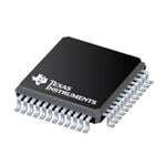
ICGOO电子元器件商城为您提供ADS7882IPFBR由Texas Instruments设计生产,在icgoo商城现货销售,并且可以通过原厂、代理商等渠道进行代购。 ADS7882IPFBR价格参考¥20.59-¥38.26。Texas InstrumentsADS7882IPFBR封装/规格:数据采集 - 模数转换器, 12 Bit Analog to Digital Converter 1 Input 1 SAR 48-TQFP (7x7)。您可以下载ADS7882IPFBR参考资料、Datasheet数据手册功能说明书,资料中有ADS7882IPFBR 详细功能的应用电路图电压和使用方法及教程。
Texas Instruments(德州仪器)的ADS7882IPFBR是一款高性能、低功耗的12位模数转换器(ADC),属于数据采集系统中的关键组件。其应用场景广泛,适用于需要高精度和快速数据采集的领域,以下是具体的应用场景:

1. 工业自动化与控制
   ADS7882IPFBR可用于工业自动化设备中,例如传感器数据采集、过程控制和监测系统。它能够将来自温度、压力、流量等传感器的模拟信号快速转换为数字信号,提供精确的数据以实现高效控制。

2. 医疗设备
   在医疗领域,该芯片适用于心电图(ECG)、脉搏血氧仪和其他便携式医疗设备。其低功耗特性和高分辨率能够确保对生物电信号的准确采集和处理。

3. 通信系统
   用于基站、调制解调器和其他通信设备中,ADS7882IPFBR可以将射频或中频信号的模拟部分转换为数字信号,支持高速数据传输和信号处理。

4. 汽车电子
   在汽车行业中,该芯片可用于车载传感器系统,如胎压监测、发动机控制单元(ECU)和自动驾驶辅助系统的信号采集模块。其可靠性和稳定性满足苛刻的车载环境要求。

5. 消费电子
   适用于音频设备、触摸屏控制器和家用智能设备。例如,在音频应用中,它可以将麦克风输入的模拟信号转换为数字信号,用于进一步处理。

6. 测试与测量仪器
   在示波器、万用表和信号分析仪等测试设备中,ADS7882IPFBR提供了高精度和快速响应能力,帮助工程师准确捕获和分析复杂信号。

总之,ADS7882IPFBR凭借其低功耗、高精度和快速转换速度的特点,成为多种应用场景下的理想选择,尤其适合对实时性和可靠性要求较高的系统设计。
| 参数 | 数值 |
| 产品目录 | 集成电路 (IC) |
| 描述 | ADC 12BIT 3MSPS LP SAR 48-TQFP |
| 产品分类 | |
| 品牌 | Texas Instruments |
| 数据手册 | |
| 产品图片 |
|
| 产品型号 | ADS7882IPFBR |
| rohs | 无铅 / 符合限制有害物质指令(RoHS)规范要求 |
| 产品系列 | - |
| 产品培训模块 | http://www.digikey.cn/PTM/IndividualPTM.page?site=cn&lang=zhs&ptm=13240 |
| 位数 | 12 |
| 供应商器件封装 | 48-TQFP(7x7) |
| 其它名称 | 296-24060-1 |
| 制造商产品页 | http://www.ti.com/general/docs/suppproductinfo.tsp?distId=10&orderablePartNumber=ADS7882IPFBR |
| 包装 | 剪切带 (CT) |
| 安装类型 | 表面贴装 |
| 封装/外壳 | 48-TQFP |
| 工作温度 | -40°C ~ 85°C |
| 数据接口 | 并联 |
| 标准包装 | 1 |
| 特性 | - |
| 电压源 | 模拟和数字 |
| 转换器数 | 1 |
| 输入数和类型 | 1 个伪差分,单极 |
| 采样率(每秒) | 3M |


- 商务部:美国ITC正式对集成电路等产品启动337调查
- 曝三星4nm工艺存在良率问题 高通将骁龙8 Gen1或转产台积电
- 太阳诱电将投资9.5亿元在常州建新厂生产MLCC 预计2023年完工
- 英特尔发布欧洲新工厂建设计划 深化IDM 2.0 战略
- 台积电先进制程称霸业界 有大客户加持明年业绩稳了
- 达到5530亿美元!SIA预计今年全球半导体销售额将创下新高
- 英特尔拟将自动驾驶子公司Mobileye上市 估值或超500亿美元
- 三星加码芯片和SET,合并消费电子和移动部门,撤换高东真等 CEO
- 三星电子宣布重大人事变动 还合并消费电子和移动部门
- 海关总署:前11个月进口集成电路产品价值2.52万亿元 增长14.8%


PDF Datasheet 数据手册内容提取
ADS7882 www.ti.com........................................................................................................................................................................................... SLAS630–DECEMBER2008 12-BIT, 3-MSPS LOW POWER SAR ANALOG-TO-DIGITAL CONVERTER FEATURES 1 • 3-MHzSampleRate,12-BitResolution DESCRIPTION • ZeroLatency The ADS7882 is a 12-bit 3-MSPS A-to-D converter • Unipolar,PseudoDifferentialInput,Range: with 2.5-V internal reference. The device includes a capacitor based SAR A/D converter with inherent – 0Vto2.5V sample and hold. The device offers a 12-bit parallel • High-SpeedParallelInterface interface with an additional byte mode that provides • 69.5dBSNRat100kHzI/P easy interface with 8-bit processors. The device has apseudo-differentialinputstage. • PowerDissipation85mWat3MSPS • NapMode(10mWPowerDissipation) The –IN swing of ±200 mV is useful to compensate for ground voltage mismatch between the ADC and • PowerDown(10m W) sensor and also to cancel common-mode noise. With • InternalReference nap mode enabled, the device operates at lower • InternalReferenceBuffer power when used at lower conversion rates. The deviceisavailablein48-pinTQFPpackage. • 48-PinTQFPPackage APPLICATIONS SAR BYTE • OpticalNetworking(DWDM,MEMSBased Output Latches Switching) +IN + and • SpectrumAnalyzers −IN _ CDAC D3-rSivteartes 12/8-Bit Parallel Comparator Data Output Bus • HighSpeedDataAcquisitionSystems REFIN • HighSpeedClose-LoopSystems CLOCK Conavnedrsion CBOUSNYVST • Telecommunication Control Logic CS REFOUT 2.5 V RD • Ultra-SoundDetection RIenfteerrennacle PWD/RST A_PWD 1 Pleasebeawarethatanimportantnoticeconcerningavailability,standardwarranty,anduseincriticalapplicationsofTexas Instrumentssemiconductorproductsanddisclaimerstheretoappearsattheendofthisdatasheet. PRODUCTIONDATAinformationiscurrentasofpublicationdate. Copyright©2008,TexasInstrumentsIncorporated Products conform to specifications per the terms of the Texas Instruments standard warranty. Production processing does not necessarilyincludetestingofallparameters.
ADS7882 SLAS630–DECEMBER2008........................................................................................................................................................................................... www.ti.com This integrated circuit can be damaged by ESD. Texas Instruments recommends that all integrated circuits be handled with appropriateprecautions.Failuretoobserveproperhandlingandinstallationprocedurescancausedamage. ESDdamagecanrangefromsubtleperformancedegradationtocompletedevicefailure.Precisionintegratedcircuitsmaybemore susceptibletodamagebecauseverysmallparametricchangescouldcausethedevicenottomeetitspublishedspecifications. ORDERINGINFORMATION(1) NOMISSING MAXIMUM MAXIMUM CODESAT PACKAGE PACKAGE TEMPERATURE ORDERING TRANSPORT MODEL INTEGRAL DIFFERENTIAL RESOLUTION TYPE DESIGNATOR RANGE INFORMATION MEDIAQUANTITY LINEARITY LINEARITY (BIT) ±4LSBat12bit 48-Pin ADS7882IPFBT Tapeandreel250 ADS7882 ±4LSBat12bit 10 PFB –40°Cto85°C (±1LSBat10bit) TQFP ADS7882IPFBR Tapeandreel1000 (1) Forthemostcurrentpackageandorderinginformation,seethePackageOptionAddendumattheendofthisdocument,orseetheTI websiteatwww.ti.com. ABSOLUTE MAXIMUM RATINGS overoperatingfree-airtemperaturerange(unlessotherwisenoted) (1) VALUE UNIT +INtoAGND –0.3to+VA+0.1 V -INtoAGND –0.3to0.5 V +VAtoAGND –0.3to7 V +VBDtoBDGND –0.3to7 V DigitalinputvoltagetoGND –0.3to(+VBD+0.3V) V DigitaloutputtoGND –0.3to(+VBD+0.3V) V Operatingtemperaturerange –40to85 °C Storagetemperaturerange –65to150 °C Junctiontemperature(Tmax) 150 °C J Powerdissipation (T Max–T )/q J A JA TQFPpackage q Thermalimpedance 86 °C/W JA Vaporphase(60sec) 215 °C Leadtemperature,soldering Infrared(15sec) 220 °C (1) Stressesbeyondthoselistedunderabsolutemaximumratingsmaycausepermanentdamagetothedevice.Thesearestressratings only,andfunctionaloperationofthedeviceattheseoranyotherconditionsbeyondthoseindicatedunderrecommendedoperating conditionsisnotimplied.Exposuretoabsolute-maximum-ratedconditionsforextendedperiodsmayaffectdevicereliability. 2 SubmitDocumentationFeedback Copyright©2008,TexasInstrumentsIncorporated ProductFolderLink(s):ADS7882
ADS7882 www.ti.com........................................................................................................................................................................................... SLAS630–DECEMBER2008 SPECIFICATIONS T =–40°Cto85°C,+VA=5V,+VBD=5Vor3.3V,V =2.5V,f =3MHz(unlessotherwisenoted) A ref sample PARAMETER TESTCONDITIONS MIN TYP MAX UNIT ANALOGINPUT Full-scaleinputspan(1) +IN–(–IN) 0 V V ref +IN –0.2 V +0.2 ref Absoluteinputrange V –IN –0.2 0.2 Inputcapacitance 27 pF Inputleakagecurrent 500 pA SYSTEMPERFORMANCE Resolution 12 Bits Nomissingcodes 10 Bits Integrallinearity(2) –4 ±1 4 LSB(3) Differentiallinearity –4 ±1 4 LSB(3) Offseterror(4) ±1 mV Gainerror(4) ±1.2 mV Withcommonmodeinputsignal=200 Common-moderejectionratio 60 dB mV at1MHz p-p AtFF0 outputcode,+VA=4.75Vto5.25 Powersupplyrejection H 80 dB V,V =2.50V ref SAMPLINGDYNAMICS +VDB=5V 280 Conversiontime nsec +VDB=3V 280 +VDB=5V 53 Acquisitiontime nsec +VDB=3V 53 Maximumthroughputrate 3 MHz Aperturedelay 2 nsec Aperturejitter 20 psec Stepresponse 50 nsec Overvoltagerecovery 50 nsec DYNAMICCHARACTERISTICS Totalharmonicdistortion(5) V =2.496V at0.1MHz/2.5V –79.5 dB IN p-p ref SNR V =2.496V at0.1MHz/2.5V 69.5 dB IN p-p ref SINAD V =2.496V at0.1MHz/2.5V 68.5 dB IN p-p ref SFDR V =2.496V at0.1MHz/2.5V 80.5 dB IN p-p ref –3dBSmallsignalbandwidth 50 MHz EXTERNALREFERENCEINPUT InputV range 2.4 2.5 2.6 V REF Resistance(6) 500 kΩ INTERNALREFERENCEOUTPUT From95%(+VA),with1-m Fstorage Start-uptime 120 msec capacitoronREFOUTtoAGND V range IOUT=0 2.425 2.5 2.575 V REF Sourcecurrent Staticload 10 m A Lineregulation +VA=4.75Vto5.25V 1 mV Drift IOUT=0 25 PPM/°C (1) Idealinputspan;doesnotincludegainoroffseterror. (2) ThisisendpointINL,notbestfit. (3) LSBmeansleastsignificantbit. (4) Measuredrelativetoactualmeasuredreference. (5) Calculatedonthefirstnineharmonicsoftheinputfrequency. (6) Canvary±20%. Copyright©2008,TexasInstrumentsIncorporated SubmitDocumentationFeedback 3 ProductFolderLink(s):ADS7882
ADS7882 SLAS630–DECEMBER2008........................................................................................................................................................................................... www.ti.com SPECIFICATIONS (continued) T =–40°Cto85°C,+VA=5V,+VBD=5Vor3.3V,V =2.5V,f =3MHz(unlessotherwisenoted) A ref sample PARAMETER TESTCONDITIONS MIN TYP MAX UNIT DIGITALINPUT/OUTPUT Logicfamily CMOS V I =5m A +V –1 +V +0.3 V IH IH BD BD V I =5m A –3 0.8 V IL IL Logiclevel V I =2TTLloads +V –0.6 +V V OH OH BD BD V I =2TTLloads 0 0.4 V OL OL Straight Dataformat Binary POWERSUPPLYREQUIREMENTS Powersupply +VBD 2.7 3.3 5.25 V voltage +VA 4.75 5 5.25 V Supplycurrent,+VA,3MHzsamplerate 17 22 mA Powerdissipation,3MHzsamplerate +VA=5V 85 110 mW NAPMODE Supplycurrent,+VA 2 3 mA Power-uptime (7) 60 nsec POWERDOWN Supplycurrent,+VA 2 2.5 m A Powerdowntime(8) Fromsimulationresults 10 m sec 1-m FstoragecapacitoronREFOUTto Poweruptime 25 msec AGND Invalidconversionsafterpoweruporreset TEMPERATURERANGE Operatingfree-air –40 85 °C (7) Minimumacquisitiontimeforfirstsamplingaftertheendofnapstatemustbe60nsecmorethannormal. (8) Timerequiredtoreachlevelof2.5m A. 4 SubmitDocumentationFeedback Copyright©2008,TexasInstrumentsIncorporated ProductFolderLink(s):ADS7882
ADS7882 www.ti.com........................................................................................................................................................................................... SLAS630–DECEMBER2008 TIMING REQUIREMENTS Allspecificationstypicalat–40°Cto85°C,+VA=+5V,+VBD=+5V (1) (2)(3) (4) PARAMETER MIN TYP MAX UNIT REFFIG. t Conversiontime 280 ns 5 (conv) t Acquisitiontime 53 ns 5 (acq) SAMPLINGANDCONVERSIONSTART t HoldtimeCSlowtoCONVSThigh(withBUSYhigh) 10 ns 3 h1 t DelayCONVSThightoacquisitionstart 2 4 5 ns 1 d1 t Holdtime,CONVSThightoCShighwithBUSYlow 10 ns 1 h2 t Holdtime,CONVSTlowtoCShigh 10 ns 1 h3 t DelayCONVSTlowtoBUSYhigh 40 ns 1 d2 t CSwidthforacquisitionorconversiontostart 20 ns 2 w3 t DelayCSlowtoacquisitionstartwithCONVSThigh 2 4 5 ns 2 d3 t Pulsewidth,fromCSlowtoCONVSTlowforacquisitiontostart 20 ns 2 w1 t DelayCSlowtoBUSYhighwithCONVSTlow 40 ns 2 d4 Quietsamplingtime(3) 25 ns CONVERSIONABORT t SetuptimeCONVSThightoCSlowwithBUSYhigh 15 ns 4 s1 t DelaytimeCSlowtoBUSYlowwithCONVSThigh 20 ns 4 d5 DATAREAD t DelayRDlowtodatavalidwithCSlow 25 ns d6 t DelayBYTEhightoLSBwordvalidwithCSandRDlow 25 ns 5 d7 t DelaytimeRDhightodata3-statewithCSlow 25 ns 5 d9 t DelaytimeendofconversiontoBUSYlow 20 ns 5 d11 t QuietsamplingtimeRDhightoCONVSTlow 20 ns 5 1 t DelayCSlowtodatavalidwithRDlow 25 ns 5 d8 t DelayCShightodata3-statewithRDlow 25 ns 6 d10 t QuietsamplingtimeCSlowtoCONVSTlow 25 ns 6 2 BACK-TO-BACKCONVERSION t DelayBUSYlowtodatavalid 10 ns 7,8 d12 t Pulsewidth,CONVSThigh 63 ns 7,8 w4 t Pulsewidth,CONVSTlow 20 ns 7 w5 POWERDOWN/RESET t Pulsewidth,lowforPWD/RSTtoresetthedevice 45 6140 ns 10 w6 t Pulsewidth,lowforPWD/RSTtopowerdownthedevice 7200 ns 9 w7 t Delaytime,powerupafterPWD/RSTishigh 25 ns 9 d13 (1) Allinputsignalsarespecifiedwitht =t =5ns(10%to90%of+VBD)andtimedfromavoltagelevelof(V +V )/2. r f IL IH (2) Seetimingdiagram. (3) Quietperiodbeforeconversionstart,nodatabusactivityincludingdatabus3-stateisallowedinthisperiod. (4) Alltimingsaremeasuredwith20pFequivalentloadsonalldatabitsandBUSYpin. Copyright©2008,TexasInstrumentsIncorporated SubmitDocumentationFeedback 5 ProductFolderLink(s):ADS7882
ADS7882 SLAS630–DECEMBER2008........................................................................................................................................................................................... www.ti.com PIN ASSIGNMENTS T T S S RD EFM EFM VA GND GND VA S D ONV YTE WD/_PW R R + A A + C R C B PA 48 47 46 45 44 43 42 41 40 39 38 37 REFIN 1 36 BUSY REFOUT 2 35 BDGND NC 3 34 +VBD +VA 4 33 NC AGND 5 32 NC +IN 6 31 NC −IN 7 30 NC AGND 8 29 DB0 +VA 9 28 DB1 +VA 10 27 DB2 AGND 11 26 DB3 AGND 12 25 BDGND 13 14 15 16 17 18 19 20 21 22 23 24 A D D 1 0 9 8 7 6 5 4 D +V AGN AGN DB1 DB1 DB DB DB DB DB DB +VB NC − No connection PINFUNCTIONS PIN I/O DESCRIPTION NAME NO.PFB 8-BITBUS 16-BITBUS DATABUS BYTE=0 BYTE=1 BYTE=0 DB11 16 O D11(MSB) D3 D11(MSB) DB10 17 O D10 D2 D10 DB9 18 O D9 D1 D9 DB8 19 O D8 D0(LSB) D8 DB7 20 O D7 0 D7 DB6 21 O D6 0 D6 DB5 22 O D5 0 D5 DB4 23 O D4 0 D4 DB3 26 O D3 0 D3 DB2 27 O D2 0 D2 DB1 28 O D1 0 D1 DB0 29 O D0(LSB) 0 D0(LSB) CONTROLPINS Chipselect.Activelowsignalenableschipoperationlikeacquisitionstart,conversionstart,bus CS 42 I releasefrom3-state.Refertothetimingdiagramsformoredetails. Conversionstart.Therisingedgestartstheacquisition.Thefallingedgeofthisinputendsthe CONVST 40 I acquisitionandstartstheconversion.Refertothetimingdiagramsformoredetails. Activelowsynchronizationpulsefortheparalleloutput.WhenCSislow,thisservesasthe RD 41 I outputenableandputsthepreviousconversionresultsonthebus. A_PWD 37 I Napmodeenable,activelow 6 SubmitDocumentationFeedback Copyright©2008,TexasInstrumentsIncorporated ProductFolderLink(s):ADS7882
ADS7882 www.ti.com........................................................................................................................................................................................... SLAS630–DECEMBER2008 PINFUNCTIONS(continued) PIN I/O DESCRIPTION NAME NO.PFB 8-BITBUS 16-BITBUS DATABUS BYTE=0 BYTE=1 BYTE=0 PWD/RST 38 I Activelowinput,actsasdevicepowerdown/deviceresetsignal. Byteselectinput.Usedfor8-bitbusreading. BYTE 39 I 0:Nofoldback 1:LowerbyteD[3:0]isfoldedbacktohighbytesoD3isavailableinD11place. STATUSOUTPUT BUSY 36 O Statusoutput.Highwhenaconversionisinprogress. POWERSUPPLY +VBD 24,34 – Digitalpowersupplyforalldigitalinputsandoutputs.RefertoTable3forlayoutguidelines. BDGND 25,35 – Digitalgroundforalldigitalinputsandoutputs.Shorttoanaloggroundplanebelowthedevice. 4,9,10,13, +VA – Analogpowersupplies.RefertoTable3forlayoutguidelines. 43,46 5,8,11,12, AGND – Analoggroundpins.Shorttoanaloggroundplanebelowthedevice. 14,15,44,45 ANALOGINPUT +IN 6 I Noninvertinganaloginputchannel –IN 7 I Invertinganaloginputchannel Reference(positive)input.NeedstobedecoupledwithREFMpinusing0.1-m Fbypasscapacitor REFIN 1 I and1-m Fstoragecapacitor. Internalreferenceoutput.TobeshortedtoREFINpinwheninternalreferenceisused.Donot REFOUT 2 O connecttoREFINpinwhenexternalreferenceisused.Alwaysneedstobedecoupledwith AGNDusing0.1-m Fbypasscapacitor. REFM 47,48 I Referenceground.Connecttoanaloggroundplane. NC – Noconnection Copyright©2008,TexasInstrumentsIncorporated SubmitDocumentationFeedback 7 ProductFolderLink(s):ADS7882
ADS7882 SLAS630–DECEMBER2008........................................................................................................................................................................................... www.ti.com DESCRIPTION AND TIMING DIAGRAMS SAMPLINGANDCONVERSIONSTART There are three ways to start sampling. The rising edge of CONVST starts sampling with CS and BUSY being low (see Figure 1) or it can be started with the falling edge of CS when CONVST is high and BUSY is low (see Figure 2). Sampling can also be started with an internal conversion end (before BUSY falling edge) with CS being low and CONVST high before an internal conversion end (see Figure 3). Also refer to the section DEVICE OPERATIONANDDATAREADINBACK-TO-BACKCONVERSIONformoredetails. A conversion can be started two ways (a conversion start is the end of sampling). Either with the falling edge of CONVST when CS is low (see Figure 1) or the falling edge of CS when CONVST is low (see Figure 2). A clean and low jitter falling edge of these respective signals triggers a conversion start and is important to the performance of the converter. The BUSY pin is brought high immediately following the CONVST falling edge. BUSYstayshighthroughouttheconversionprocessandreturnslowwhentheconversionhasended. th2 th3 CS CONVST td1 td2 BUSY t(acq) Figure1.SamplingandConversionStartControlWithCONVSTPin tw3 tw3 CS td4 CONVST td3 tw1 BUSY t(acq) Figure2.SamplingandConversionStartControlWithCSPin CS th1 tw5 CONVST tw4 BUSY td2 t(acq) Figure3.SamplingStartWithCSLowandCONVSTHigh(Back-to-Back) 8 SubmitDocumentationFeedback Copyright©2008,TexasInstrumentsIncorporated ProductFolderLink(s):ADS7882
ADS7882 www.ti.com........................................................................................................................................................................................... SLAS630–DECEMBER2008 CONVERSIONABORT The falling edge of CS aborts the conversion while BUSY is high and CONVST is high (see Figure 4). The deviceoutputsFE0(hex)toindicateaconversionabort. td5 BUSY tsu1 CONVST CS RD D11−D0 1111 1110 0000 Figure4.ConversionAbort DATAREAD Two conditions need to be satisfied for a read operation. Data appears on the D11 through D0 pins (with D11 MSB) when both CS and RD are low. Figure 5 and Figure 6 illustrate the device read operation. The bus is 3-statedifanyoneofthesignalsishigh. td2 t1 tw5 CONVST t(conv) td1 + t(acq) BUSY td11 CS RD BYTE td6 td7 td9 D11−D0 D11−4 & D3−0 D3−0 Figure5.ReadControlviaCSandRD There are two output formats available. Twelve bit data appears on the bus during a read operation while BYTE is low. When BYTE is high, the lower byte (D3 through D0 followed by all zeroes) appears on the data bus with D3intheMSB.Thisfeatureisusefulforinterfacingwitheightbitmicroprocessorsandmicrocontrollers. Copyright©2008,TexasInstrumentsIncorporated SubmitDocumentationFeedback 9 ProductFolderLink(s):ADS7882
ADS7882 SLAS630–DECEMBER2008........................................................................................................................................................................................... www.ti.com t2 CONVST BUSY td1 + t(acq) Conversion No N td2 CS BYTE td7 td10 D11−D0 D11−4 & D3−0 D3−0 Data For Conv. N−1 Data For Conv. N td8 Figure6.ReadControlViaCSandRDTiedtoBDGND DEVICEOPERATIONANDDATAREADINBACK-TO-BACKCONVERSION Figure 7 and Figure 8 illustrate device operation in back-to-back conversion mode. It is possible to operate the device at any throughput in this mode, but this is the only mode in which the device can be operated at throughputsexceeding2.83MSPS(1/t min+t max+t max)). (acq) (conv) d11 A conversion starts on the CONVST falling edge. The BUSY output goes high after a delay (t ). Note that care d2 must be taken not to abort the conversion (see Figure 4) apart from timing restrictions shown in Figure 7 and Figure 8. The conversion ends within the conversion time, t , after the CONVST falling edge. The new (conv) acquisition can be immediately started without waiting for the BUSY signal to go low. This can be ensured with a CONVSThighpulsewidththatismorethanorequalto(t –t +10nsec)whichist fora3-MHzoperation. 0 (conv) w4 Sample N CONVST tw4 tw5 t(acq) Conversion N BUSY td12 t(conv) + td11 D11−D0 Data For Conversion N−1 (Data Read without Latency) t0 = 333 ns for 3 MSPS Operation Figure7.Back-To-BackOperationWithCSandRDLow 10 SubmitDocumentationFeedback Copyright©2008,TexasInstrumentsIncorporated ProductFolderLink(s):ADS7882
ADS7882 www.ti.com........................................................................................................................................................................................... SLAS630–DECEMBER2008 CS th1 Sample N CONVST tw4 tw3 t(acq) t(conv) + td11 Conversion N BUSY td12 Data For Conversion N−1 D11−D0 (Data Read without Latency) t0 = 333 ns for 3 MSPS Operation Figure8.Back-To-BackoperationWithCSTogglingandRDLow NAPMODE The device can be put in nap mode following the sequences shown in Figure 9. This provides substantial power savingwhileoperatingatlowersamplingrates. Whileoperatingthedeviceatthroughputrateslowerthan2.54MSPS,A_PWDcan be held low (see Figure 9). In thiscondition, the device goes into the nap state immediately after BUSY goes low and remains in that state until the next sampling starts. The minimum acquisition time is 60 nsec more than t as defined in the timing (acq) requirementssection. Alternately, A_PWD can be toggled any time during operation (see Figure 10). This is useful when the system acquires data at the maximum conversion speed for some period of time (back-to-back conversion) and it does not acquire data for some time while the acquired data is being processed. During this period, the device can be put in the nap state to save power. The device remains in the nap state as long as A_PWD is low with BUSY being low and sampling has not started. The minimum acquisition time for the first sampling after the nap state is 60nsecmorethant asdefinedinthetimingrequirementssection. (acq) A_PWD (Held Low) BUSY SAMPLE (Internal) t(acq) + 60 ns NAP (Internal Active High) NOTE: The SAMPLE (Internal) signal is generated as described in the Sampling and Conversion Start section. Figure9.DeviceOperationWhileA_PWDisHeldLow Copyright©2008,TexasInstrumentsIncorporated SubmitDocumentationFeedback 11 ProductFolderLink(s):ADS7882
ADS7882 SLAS630–DECEMBER2008........................................................................................................................................................................................... www.ti.com A_PWD BUSY SAMPLE (Internal) t(acq) + 60 ns NAP (Internal Active High) NOTE: The SAMPLE (Internal) signal is generated as described in the Sampling and Conversion Start section. Figure10.DeviceOperationWhileA_PWDisToggling POWERDOWN/RESET A low level on the PWD/RST pin puts the device in the powerdown phase. This is an asynchronous signal. As shown in Figure 11, the device is in the reset phase for the first t period after a high-to-low transition of w6 PWD/RST. During this period the output code is FE0 (hex) to indicate that the device is in the reset phase. The device powers down if the PWD/RST pin continues to be low for a period of more than t . Data is not valid for w7 the first four conversions after a power-up (see Figure 11) or an end of reset (see Figure 12). The device is initializedduringthefirstfourconversions. tw7 PWD/RST Valid Conversions First 4 Invalid Conversions BUSY 1 2 3 4 5 td13 D11−D0 1111 1110 0000 Power Down RESET Phase Phase Invalid Data Valid Data Figure11.DevicePowerDown tw6 45 ns PWD/RST Valid Conversions First 4 Invalid Conversions BUSY 1 2 3 4 5 D11−D0 1111 1110 0000 RESET Phase Invalid Data Valid Data Figure12.DeviceReset 12 SubmitDocumentationFeedback Copyright©2008,TexasInstrumentsIncorporated ProductFolderLink(s):ADS7882
ADS7882 www.ti.com........................................................................................................................................................................................... SLAS630–DECEMBER2008 TYPICAL CHARACTERISTICS(1) EFFECTIVENUMBEROFBITS HISTOGRAM vs (DCCODESPREADCLOSETOZEROINPUT) FREE-AIRTEMPERATURE 5000 11.24 4692 TA = 25°C 4500 Throughput = 3 MSPS 11.22 4000 VA = 5 V Bits VREF = 2.5 V − 11.20 z 3500 Bits − kH 3000 er of 11.18 y b c m uen 2500 Nu 11.16 q e − Fre 2000 ectiv 11.14 f 1500 Eff − B 11.12 1000 O fIN = 100 kHz N E 11.10 Throughput = 3 MSPS 500 308 VA = 5 V VREF = 2.5 V 0 11.08 28 29 −40 −20 0 20 40 60 80 Bin TA − Free-Air temperature − °C G001 G002 Figure13. Figure14. SIGNAL-TO-NOISEANDDISTORTION SIGNAL-TO-NOISERATIO vs vs FREE-AIRTEMPERATURE FREE-AIRTEMPERATURE 70.0 71.0 fIN = 100 kHz fIN = 100 kHz dB Throughput = 3 MSPS Throughput = 3 MSPS ortion − 69.5 VVAR E=F 5 = V 2.5 V − dB 70.5 VVAR E=F 5 = V 2.5 V Dist atio 70.0 d R e an oise Nois 69.0 o-N 69.5 al-to- gnal-t n Si 69.0 D− Sig 68.5 SNR− A 68.5 N SI 68.0 68.0 −40 −20 0 20 40 60 80 −40 −20 0 20 40 60 80 TA − Free-Air temperature − °C TA − Free-Air temperature − °C G003 G004 Figure15. Figure16. (1) Atsamplerate=3MSPS,V =2.5Vexternal,unlessotherwisespecified. ref Copyright©2008,TexasInstrumentsIncorporated SubmitDocumentationFeedback 13 ProductFolderLink(s):ADS7882
ADS7882 SLAS630–DECEMBER2008........................................................................................................................................................................................... www.ti.com TOTALHARMONICDISTORTION SPURIOUS-FREEDYNAMICRANGE vs vs FREE-AIRTEMPERATURE FREE-AIRTEMPERATURE −78.0 82.0 fIN = 25°C Throughput = 3 MSPS dB dB −78.5 VA = 5 V e − − VREF = 2.5 V ng 81.5 n a o R Distorti −79.0 namic onic −79.5 e Dy 81.0 m e Har s-Fr Total −80.0 puriou − S 80.5 THD −80.5 DR− fTINh r=o u2g5h°pCut = 3 MSPS SF VA = 5 V VREF = 2.5 V −81.0 80.0 −40 −20 0 20 40 60 80 −40 −20 0 20 40 60 80 TA − Free-Air temperature − °C TA − Free-Air temperature − °C G005 G006 Figure17. Figure18. EFFECTIVENUMBEROFBITS SIGNAL-TO-NOISEANDDISTORTION vs vs INPUTFREQUENCY INPUTFREQUENCY 11.5 72 TA = 25°C B Throughput = 3 MSPS d Bits − Bits 11.3 stortion − 71 VVAR E=F 5 = V 2.5 V er of 11.1 nd Di 70 b a m e u s N oi ective 10.9 al-to-N 69 Eff gn − Si OB 10.7 TA = 25°C D− 68 EN Throughput = 3 MSPS NA VA = 5 V SI VREF = 2.5 V 10.5 67 1 10 100 1 10 100 fIN − Input Frequency − kHz fIN − Input Frequency − kHz G007 G008 Figure19. Figure20. 14 SubmitDocumentationFeedback Copyright©2008,TexasInstrumentsIncorporated ProductFolderLink(s):ADS7882
ADS7882 www.ti.com........................................................................................................................................................................................... SLAS630–DECEMBER2008 SIGNAL-TO-NOISERATIO TOTALHARMONICDISTORTION vs vs INPUTFREQUENCY INPUTFREQUENCY 72.0 −78.0 TA = 25°C Throughput = 3 MSPS 71.5 B −78.5 VA = 5 V dB − d VREF = 2.5 V − n atio 71.0 ortio −79.0 e R Dist Nois 70.5 nic −79.5 o- mo nal-t Har − Sig 70.0 Total −80.0 R − SN TA = 25°C HD 69.5 Throughput = 3 MSPS T −80.5 VA = 5 V VREF = 2.5 V 69.0 −81.0 1 10 100 1 10 100 fIN − Input Frequency − kHz fIN − Input Frequency − kHz G009 G010 Figure21. Figure22. SPURIOUS-FREEDYNAMICRANGE OFFSETERROR vs vs INPUTFREQUENCY FREE-AIRTEMPERATURE 87.0 2.0 TA = 25°C Throughput = 3 MSPS dB 86.5 Throughput = 3 MSPS 1.5 VA = 5 V e − VA = 5 V VREF = 2.5 V ng 86.0 VREF = 2.5 V 1.0 a R c mi 85.5 mV 0.5 na − ee Dy 85.0 Error 0.0 Fr et ous- 84.5 Offs −0.5 uri p S 84.0 −1.0 − R D F 83.5 −1.5 S 83.0 −2.0 1 10 100 −40 −20 0 20 40 60 80 fIN − Input Frequency − kHz TA − Free-Air temperature − °C G011 G012 Figure23. Figure24. Copyright©2008,TexasInstrumentsIncorporated SubmitDocumentationFeedback 15 ProductFolderLink(s):ADS7882
ADS7882 SLAS630–DECEMBER2008........................................................................................................................................................................................... www.ti.com GAINERROR INTEGRALNONLINEARITY vs vs FREE-AIRTEMPERATURE FREE-AIRTEMPERATURE 2.0 4 Throughput = 3 MSPS Throughput = 3 MSPS 1.5 VA = 5 V 3 VA = 5 V VREF = 2.5 V VREF = 2.5 V B 1.0 S 2 L − − LSB 0.5 nearity 1 Max n Error 0.0 al Nonli 0 ai −0.5 gr −1 G e Min nt − I −1.0 L −2 N I −1.5 −3 −2.0 −4 −40 −20 0 20 40 60 80 −40 −20 0 20 40 60 80 TA − Free-Air temperature − °C TA − Free-Air temperature − °C G013 G014 Figure25. Figure26. DIFFERENTIALNONLINEARITY REFERENCEOUTPUTDRIFT vs vs FREE-AIRTEMPERATURE FREE-AIRTEMPERATURE 4 7 Throughput = 3 MSPS Throughput = 3 MSPS 3 VA = 5 V 6 VA = 5 V B VREF = 2.5 V S 5 nearity − L 12 Max Drift − mV 4 onli ut 3 N 0 p al Out 2 nti e Differe −1 Min erenc 1 L − −2 Ref 0 N D −3 −1 −4 −2 −40 −20 0 20 40 60 80 −40 −20 0 20 40 60 80 TA − Free-Air temperature − °C TA − Free-Air temperature − °C G015 G016 Figure27. Figure28. 16 SubmitDocumentationFeedback Copyright©2008,TexasInstrumentsIncorporated ProductFolderLink(s):ADS7882
ADS7882 www.ti.com........................................................................................................................................................................................... SLAS630–DECEMBER2008 POWERDISSIPATION vs SAMPLERATE 90 80 70 W m − 60 n o ati 50 p si s Di 40 er w Po 30 − D P 20 TA = 25°C 10 VA = 5 V VREF = 2.5 V 0 0 500 1000 1500 2000 2500 3000 Sample Rate − KSPS G017 Figure29. DIFFERENTIALNONLINEARITY 1.0 SB 0.8 TTAh r=o u2g5h°pCut = 3 MSPS L arity − 00..46 VVAR E=F 5 = V 2.5 V e n nli 0.2 o N 0.0 al nti −0.2 e er −0.4 Diff − −0.6 L N −0.8 D −1.0 0 1024 2048 3072 4096 Code G018 Figure30. Copyright©2008,TexasInstrumentsIncorporated SubmitDocumentationFeedback 17 ProductFolderLink(s):ADS7882
ADS7882 SLAS630–DECEMBER2008........................................................................................................................................................................................... www.ti.com INTEGRALNONLINEARITY 1.0 0.8 TA = 25°C B Throughput = 3 MSPS S L 0.6 VA = 5 V y − 0.4 VREF = 2.5 V arit e 0.2 n onli 0.0 N al −0.2 gr nte −0.4 − I −0.6 L N I −0.8 −1.0 0 1024 2048 3072 4096 Code G019 Figure31. FFT 0 −20 TA = 25°C Throughput = 3 MSPS −40 VA = 5 V B −60 VREF = 2.5 V d − er −80 w o −100 P − P −120 −140 −160 −180 0 300 600 900 1200 1500 f − Frequency − kHz G020 Figure32. PRINCIPLES OF OPERATION The ADS7882 is a member of a family of high-speed successive approximation register (SAR) analog-to-digital converters (ADC). The architecture is based on charge redistribution, which inherently includes a sample/hold function. Theconversionclockisgeneratedinternally.Theconversiontimeis200nsmax(at5V+VBD). The analog input is provided to two input pins: +IN and –IN. (Note that this is pseudo differential input and there are restrictions on –IN voltage range.) When a conversion is initiated, the difference voltage between these pins is sampled on the internal capacitor array. While a conversion is in progress, both inputs are disconnected from anyinternalfunction. REFERENCE The ADS7882 has a built-in 2.5-V (nominal value) reference but can operate with an external reference. When an internal reference is used, pin 2 (REFOUT) should be connected to pin 1 (REFIN) with an 0.1-m F decoupling capacitoranda1-m Fstoragecapacitorbetweenpin2 (REFOUT) and pins 47, 48 (REFM). The internal reference of the converter is buffered . There is also a buffer from REFIN to CDAC. This buffer provides isolation between theexternalreferenceandtheCDACandalsorechargestheCDACduringconversion. It is essential to decouple REFOUTtoAGNDwitha0.1-m Fcapacitorwhilethedeviceoperateswithanexternalreference. 18 SubmitDocumentationFeedback Copyright©2008,TexasInstrumentsIncorporated ProductFolderLink(s):ADS7882
ADS7882 www.ti.com........................................................................................................................................................................................... SLAS630–DECEMBER2008 PRINCIPLES OF OPERATION (continued) ANALOG INPUT When the converter enters hold mode, the voltage difference between the +IN and -IN inputs is captured on the internal capacitor array. The voltage on the –IN input is limited to between –0.2 V and 0.2 V, thus allowing the input to reject a small signal which is common to both the +IN and -IN inputs. The +IN input has a range of –0.2 Vto(+Vref+0.2V).Theinputspan(+IN–(–IN))islimitedfrom0VtoVREF. The input current on the analog inputs depends upon a number of factors: sample rate, input voltage, signal frequency, and source impedance. Essentially, the current into the ADS7882 charges the internal capacitor array during the sample period. After this capacitance has been fully charged, there is no further input current (this may not happen when a signal is moving continuously). The source of the analog input voltage must be able to charge the input capacitance (27 pF) to better than a 12-bit settling level with a step input within the acquisition time of the device. The step size can be selected equal to the maximum voltage difference between two consecutivesamplesatthemaximumsignalfrequency.(RefertoFigure35forthesuggestedinput circuit.) When theconvertergoesintoholdmode,theinputimpedanceisgreaterthan1GΩ. Care must be taken regarding the absolute analog input voltage. To maintain the linearity of the converter, both –IN and +IN inputs should be within the limits specified. Outside of these ranges, the converter's linearity may notmeetspecifications. Care should be taken to ensure that +IN and -IN see the same impedance to the respective sources. (For example, both +IN and –IN are connected to a decoupling capacitor through a 21-Ω resistor as shown in Figure 35.) If this is not observed, the two inputs could have different settling times. This may result in an offset error,gainerror,orlinearityerrorwhichchangeswithtemperatureandinputvoltage. DIGITAL INTERFACE TIMINGANDCONTROL RefertotheSAMPLINGANDCONVERSIONSTARTsectionandtheCONVERSIONABORTsection. READINGDATA The ADS7882 outputs full parallel data in straight binary format as shown in Table 1. The parallel output is active when CS and RD are both low. There is a minimal quiet sampling period requirement around the falling edge of CONVST as stated in the timing requirements section. Data reads or bus three-state operations should not be attempted within this period. Any other combination of CS and RD 3-states the parallel output. Refer to Table 1 foridealoutputcodes. Table1.IdealInputVoltagesandOutputCodes(1) DESCRIPTION ANALOGVALUE BINARYCODE HEXCODE Fullscale V –1LSB 111111111111 FFF ref Midscale V /2 100000000000 800 ref Midscale–1LSB V /2–1LSB 011111111111 7FF ref Zero 0V 000000000000 000 (1) Full-scalerange=V andleastsignificantbit(LSB)=V /4096 ref ref Theoutputdataappearsasafull12-bitword(D11–D0)onpinsDB11–DB0(MSB–LSB)ifBYTEislow. READINGTHEDATAINBYTEMODE The result can also be read on an 8-bit bus for convenience by using pins DB11–DB4. In this case two reads are necessary; the first as before, leaving BYTE low and reading the 8 most significant bits on pins DB11–DB4, and then bringing BYTE high. When BYTE is high, the lower bits (D3–D0) followed by all zeros are on pins DB11–DB4(refertoTable2). These multi-word read operations can be performed with multiple active RD signals (toggling) or with RD tied low forsimplicity. Copyright©2008,TexasInstrumentsIncorporated SubmitDocumentationFeedback 19 ProductFolderLink(s):ADS7882
ADS7882 SLAS630–DECEMBER2008........................................................................................................................................................................................... www.ti.com Table2.ConversionDataReadOut DATAREADOUT BYTE DB11–DB4 DB3–DB0 High D3–D0,0000 Allzeroes Low D11–D4 D3–D0 Also refer to the DATA READ and DEVICE OPERATION AND DATA READ IN BACK-TO-BACK CONVERSION sectionsformoredetails. Reset RefertothePOWERDOWN/RESETsectionforthedeviceresetsequence. Itisrecommendedtoresetthedeviceafterpower on. A reset can be issued once the power has reached 95% of itsfinalvalue. PWD/RST is an asynchronous active low input signal. A current conversion is aborted no later than 45 ns after the converter is in the reset mode. In addition, the device outputs a FE0 code to indicate a reset condition. The converterreturnsbacktonormaloperationmodeimmediatelyafterthePWD/RSTinputisbroughthigh. Dataisnotvalidforthefirstfourconversionsafteradevicereset. Powerdown RefertothePOWERDOWN/RESETsectionforthedevicepowerdownsequence. ThedeviceenterspowerdownmodeifaPWD/RSTlowdurationisextendedformorethanaperiodoft . w7 The converter goes back to normal operation mode no later than a period of t after the PWD/RST input is d13 broughthigh. After this period, normal conversion and sampling operation can be started as discussed in previous sections. Dataisnotvalidforthefirstfourconversionsafteradevicereset. NapMode RefertotheNAPMODEsectionintheDESCRIPTIONANDTIMINGDIAGRAMSsectionforinformation. 20 SubmitDocumentationFeedback Copyright©2008,TexasInstrumentsIncorporated ProductFolderLink(s):ADS7882
ADS7882 www.ti.com........................................................................................................................................................................................... SLAS630–DECEMBER2008 APPLICATION INFORMATION LAYOUT Foroptimumperformance,careshouldbetakenwiththephysicallayoutoftheADS7882circuitry. As the ADS7882 offers single-supply operation, it is often used in close proximity with digital logic, micro-controllers,microprocessors,anddigitalsignalprocessors.Themore digital logic present in the design and thehighertheswitchingspeed,themoredifficultitistoachieveacceptableperformancefromtheconverter. The basic SAR architecture is sensitive to glitches or sudden changes on the power supply, reference, ground connections, and digital inputs that occur just prior to the end of sampling (within quiet sampling time) and just prior to latching the output of the analog comparator during the conversion phase. Thus, driving any single conversion for an n-bit SAR converter, there are n+1 windows in which large external transient voltages can affect the conversion result. Such glitches might originate from switching power supplies, nearby digital logic, or highpowerdevices. The degree of error in the digital output depends on the reference voltage, layout, and the exact timing of the externalevent. On average, the ADS7882 draws very little current from an external reference as the reference voltage is internally buffered. If the reference voltage is external and originates from an op amp, make sure that it can drive the bypass capacitor or capacitors without oscillation. A 0.1-m F bypass capacitor and 1-m F storage capacitor are recommendedfromREFIN(pin1)directlytoREFM(pin48). The AGND and BDGND pins should be connected to a clean ground point. In all cases, this should be the analogground.Avoidconnectionswhicharetoo close to the grounding point of a micro-controller or digital signal processor. If required, run a ground trace directly from the converter to the power supply entry point. The ideal layoutconsistsofananaloggroundplanededicatedtotheconverterandassociatedanalogcircuitry. As with the AGND connections, +VA should be connected to a 5-V power supply plane that is separate from the connection for +VBD and digital logic until they are connected at the power entry point onto the PCB. Power to the ADS7882 should be clean and well bypassed. A 0.1-m F ceramic bypass capacitor should be placed as close to the device as possible. See Table 3 for the placement of capacitor. In addition to a 0.1-m F capacitor, a 1-m F capacitor is recommended. In some situations, additional bypassing may be required, such as a 100-m F electrolytic capacitor or even a Pi filter made up of inductors and capacitors, all designed to essentially low-pass filterthe5-Vsupply,removingthehighfrequencynoise. Table3.PowerSupplyDecouplingCapacitorPlacement POWERSUPPLYPLANE CONVERTER CONVERTERANALOGSIDE DIGITALSIDE SUPPLYPINS Pairsofpinsthatrequireashortestpathtodecoupling (4,5),(9,8),(10,11),(13,15),(43,44)(46,45) (24,25),(34,35) capacitors Pinsthatrequirenodecoupling 14,12 Analog 5 V +VA 1 m F 0.1 m F ADS7882 AGND AGND 0.1 m F REFOUT External Reference from REFIN REF5025 or REF3225 1 m F 0.1 m F AGND REFM 21 W Analog Input +IN Circuit 21 W −IN Figure33.UsingExternalReference Copyright©2008,TexasInstrumentsIncorporated SubmitDocumentationFeedback 21 ProductFolderLink(s):ADS7882
ADS7882 SLAS630–DECEMBER2008........................................................................................................................................................................................... www.ti.com Analog 5 V +VA 1 m F 0.1 m F ADS7882 AGND AGND REFOUT REFIN 1 m F 0.1 m F AGND REFM 21 W +IN Analog Input Circuit 21 W −IN Figure34.UsingInternalReference 130 pF 604 W Signal Input, Bipolar, (cid:1)1.25 V 604 W _ 12 W 21 W 2.5 V DC 3 kW 100 W THS4031 +IN + 150 pF 21 W ADS7882 −IN 1 kW 1 nF AGND AGND Figure35.TypicalAnalogInputCircuitforBipolarSignal 50W _ 12W 21W THS4031 +IN Signal Input Unipolar 0 V–2.5 V + 150 pF 21W ADS7882 –IN Figure36.TypicalApplicationInputCircuitforUnipolarSignal 22 SubmitDocumentationFeedback Copyright©2008,TexasInstrumentsIncorporated ProductFolderLink(s):ADS7882
ADS7882 www.ti.com........................................................................................................................................................................................... SLAS630–DECEMBER2008 GPIO CS GPIO BYTE GPIO CONVST Microcontroller ADS7882 P[7:0] DB[11:4] RD RD INT BUSY Figure37.InterfacingWithMicrocontroller Copyright©2008,TexasInstrumentsIncorporated SubmitDocumentationFeedback 23 ProductFolderLink(s):ADS7882
PACKAGE OPTION ADDENDUM www.ti.com 6-Feb-2020 PACKAGING INFORMATION Orderable Device Status Package Type Package Pins Package Eco Plan Lead/Ball Finish MSL Peak Temp Op Temp (°C) Device Marking Samples (1) Drawing Qty (2) (6) (3) (4/5) ADS7882IPFBR ACTIVE TQFP PFB 48 1000 Green (RoHS NIPDAU Level-2-260C-1 YEAR -40 to 85 ADS7882 & no Sb/Br) ADS7882IPFBT ACTIVE TQFP PFB 48 250 Green (RoHS NIPDAU Level-2-260C-1 YEAR -40 to 85 ADS7882 & no Sb/Br) (1) The marketing status values are defined as follows: ACTIVE: Product device recommended for new designs. LIFEBUY: TI has announced that the device will be discontinued, and a lifetime-buy period is in effect. NRND: Not recommended for new designs. Device is in production to support existing customers, but TI does not recommend using this part in a new design. PREVIEW: Device has been announced but is not in production. Samples may or may not be available. OBSOLETE: TI has discontinued the production of the device. (2) RoHS: TI defines "RoHS" to mean semiconductor products that are compliant with the current EU RoHS requirements for all 10 RoHS substances, including the requirement that RoHS substance do not exceed 0.1% by weight in homogeneous materials. Where designed to be soldered at high temperatures, "RoHS" products are suitable for use in specified lead-free processes. TI may reference these types of products as "Pb-Free". RoHS Exempt: TI defines "RoHS Exempt" to mean products that contain lead but are compliant with EU RoHS pursuant to a specific EU RoHS exemption. Green: TI defines "Green" to mean the content of Chlorine (Cl) and Bromine (Br) based flame retardants meet JS709B low halogen requirements of <=1000ppm threshold. Antimony trioxide based flame retardants must also meet the <=1000ppm threshold requirement. (3) MSL, Peak Temp. - The Moisture Sensitivity Level rating according to the JEDEC industry standard classifications, and peak solder temperature. (4) There may be additional marking, which relates to the logo, the lot trace code information, or the environmental category on the device. (5) Multiple Device Markings will be inside parentheses. Only one Device Marking contained in parentheses and separated by a "~" will appear on a device. If a line is indented then it is a continuation of the previous line and the two combined represent the entire Device Marking for that device. (6) Lead/Ball Finish - Orderable Devices may have multiple material finish options. Finish options are separated by a vertical ruled line. Lead/Ball Finish values may wrap to two lines if the finish value exceeds the maximum column width. Important Information and Disclaimer:The information provided on this page represents TI's knowledge and belief as of the date that it is provided. TI bases its knowledge and belief on information provided by third parties, and makes no representation or warranty as to the accuracy of such information. Efforts are underway to better integrate information from third parties. TI has taken and continues to take reasonable steps to provide representative and accurate information but may not have conducted destructive testing or chemical analysis on incoming materials and chemicals. TI and TI suppliers consider certain information to be proprietary, and thus CAS numbers and other limited information may not be available for release. In no event shall TI's liability arising out of such information exceed the total purchase price of the TI part(s) at issue in this document sold by TI to Customer on an annual basis. Addendum-Page 1
PACKAGE OPTION ADDENDUM www.ti.com 6-Feb-2020 Addendum-Page 2
PACKAGE MATERIALS INFORMATION www.ti.com 26-Feb-2019 TAPE AND REEL INFORMATION *Alldimensionsarenominal Device Package Package Pins SPQ Reel Reel A0 B0 K0 P1 W Pin1 Type Drawing Diameter Width (mm) (mm) (mm) (mm) (mm) Quadrant (mm) W1(mm) ADS7882IPFBR TQFP PFB 48 1000 330.0 16.4 9.6 9.6 1.5 12.0 16.0 Q2 ADS7882IPFBT TQFP PFB 48 250 180.0 16.4 9.6 9.6 1.5 12.0 16.0 Q2 PackMaterials-Page1
PACKAGE MATERIALS INFORMATION www.ti.com 26-Feb-2019 *Alldimensionsarenominal Device PackageType PackageDrawing Pins SPQ Length(mm) Width(mm) Height(mm) ADS7882IPFBR TQFP PFB 48 1000 350.0 350.0 43.0 ADS7882IPFBT TQFP PFB 48 250 213.0 191.0 55.0 PackMaterials-Page2
MECHANICAL DATA MTQF019A – JANUARY 1995 – REVISED JANUARY 1998 PFB (S-PQFP-G48) PLASTIC QUAD FLATPACK 0,27 0,50 0,08 M 0,17 36 25 37 24 48 13 0,13 NOM 1 12 5,50 TYP 7,20 SQ Gage Plane 6,80 9,20 SQ 8,80 0,25 0,05 MIN 0°–7° 1,05 0,95 0,75 Seating Plane 0,45 0,08 1,20 MAX 4073176/B 10/96 NOTES: A. All linear dimensions are in millimeters. B. This drawing is subject to change without notice. C. Falls within JEDEC MS-026 • POST OFFICE BOX 655303 DALLAS, TEXAS 75265
None
IMPORTANTNOTICEANDDISCLAIMER TI PROVIDES TECHNICAL AND RELIABILITY DATA (INCLUDING DATASHEETS), DESIGN RESOURCES (INCLUDING REFERENCE DESIGNS), APPLICATION OR OTHER DESIGN ADVICE, WEB TOOLS, SAFETY INFORMATION, AND OTHER RESOURCES “AS IS” AND WITH ALL FAULTS, AND DISCLAIMS ALL WARRANTIES, EXPRESS AND IMPLIED, INCLUDING WITHOUT LIMITATION ANY IMPLIED WARRANTIES OF MERCHANTABILITY, FITNESS FOR A PARTICULAR PURPOSE OR NON-INFRINGEMENT OF THIRD PARTY INTELLECTUAL PROPERTY RIGHTS. These resources are intended for skilled developers designing with TI products. You are solely responsible for (1) selecting the appropriate TI products for your application, (2) designing, validating and testing your application, and (3) ensuring your application meets applicable standards, and any other safety, security, or other requirements. These resources are subject to change without notice. TI grants you permission to use these resources only for development of an application that uses the TI products described in the resource. Other reproduction and display of these resources is prohibited. No license is granted to any other TI intellectual property right or to any third party intellectual property right. TI disclaims responsibility for, and you will fully indemnify TI and its representatives against, any claims, damages, costs, losses, and liabilities arising out of your use of these resources. TI’s products are provided subject to TI’s Terms of Sale (www.ti.com/legal/termsofsale.html) or other applicable terms available either on ti.com or provided in conjunction with such TI products. TI’s provision of these resources does not expand or otherwise alter TI’s applicable warranties or warranty disclaimers for TI products. Mailing Address: Texas Instruments, Post Office Box 655303, Dallas, Texas 75265 Copyright © 2020, Texas Instruments Incorporated