ICGOO在线商城 > 集成电路(IC) > 数据采集 - 模数转换器 > ADS1114IRUGT
 Datasheet下载
- 型号: ADS1114IRUGT
- 制造商: Texas Instruments
- 库位|库存: xxxx|xxxx
- 要求:
| 数量阶梯 | 香港交货 | 国内含税 |
| +xxxx | $xxxx | ¥xxxx |
查看当月历史价格
查看今年历史价格
ADS1114IRUGT产品简介:
ICGOO电子元器件商城为您提供ADS1114IRUGT由Texas Instruments设计生产,在icgoo商城现货销售,并且可以通过原厂、代理商等渠道进行代购。 ADS1114IRUGT价格参考¥34.64-¥48.57。Texas InstrumentsADS1114IRUGT封装/规格:数据采集 - 模数转换器, 16 Bit Analog to Digital Converter 1, 2 Input 1 Sigma-Delta 10-X2QFN (2x1.5)。您可以下载ADS1114IRUGT参考资料、Datasheet数据手册功能说明书,资料中有ADS1114IRUGT 详细功能的应用电路图电压和使用方法及教程。
Texas Instruments(德州仪器)的ADS1114IRUGT是一款16位、低功耗、delta-sigma模数转换器(ADC),广泛应用于需要高精度和低功耗的数据采集场景。以下是该型号的主要应用场景:

 1. 工业自动化与控制
   - ADS1114IRUGT可用于工业传感器信号的精确采集,例如温度、压力、湿度或流量传感器。
   - 在工业控制系统中,它能够将模拟信号转换为数字信号,以便进行实时监控和分析。

 2. 医疗设备
   - 适用于便携式医疗设备,如血压计、血糖仪或心率监测仪。
   - 其高分辨率和低功耗特性非常适合电池供电的医疗设备,确保长时间运行并提供准确的测量结果。

 3. 环境监测
   - 可用于环境监测系统,例如空气质量检测、水污染监测或气象站。
   - 能够精确采集来自各种传感器(如气体传感器、温湿度传感器)的微弱信号,并将其转换为可处理的数字数据。

 4. 消费电子
   - 在智能家居设备中,用于采集环境参数(如光照强度、室内温湿度)以实现智能控制。
   - 适用于健康追踪设备,如智能手环或智能秤,提供高精度的体征数据采集。

 5. 农业与物联网
   - 在精准农业中,用于土壤湿度、pH值或光照强度的监测。
   - 结合物联网技术,将采集到的数据上传至云端,实现远程监控和智能化管理。

 6. 能源管理
   - 应用于电力监测设备,如电表或电流电压传感器,用于精确测量能耗。
   - 其低功耗设计适合电池供电的能源管理系统,延长设备使用寿命。

 7. 实验室与科研
   - 在实验环境中,用于高精度数据采集,例如物理量(电压、电流)或化学量(pH值、溶解氧)的测量。
   - 提供稳定可靠的性能,支持科研人员进行数据分析和验证。

ADS1114IRUGT凭借其小尺寸、低功耗和高精度的特点,特别适合对成本敏感且需要简单易用解决方案的应用场合。
| 参数 | 数值 |
| 产品目录 | 集成电路 (IC)半导体 |
| 描述 | IC ADC 16-BIT I2C PROGBL 10-QFN模数转换器 - ADC 16B ADC w/ Int MUX PGA Comp Osc & Ref |
| 产品分类 | |
| 品牌 | Texas Instruments |
| 产品手册 | |
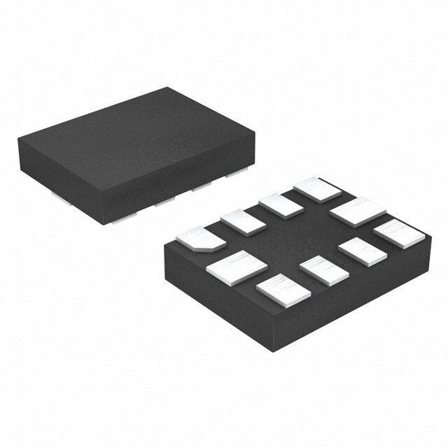
| 产品图片 |
|
| rohs | 符合RoHS无铅 / 符合限制有害物质指令(RoHS)规范要求 |
| 产品系列 | 数据转换器IC,模数转换器 - ADC,Texas Instruments ADS1114IRUGT- |
| 数据手册 | 点击此处下载产品Datasheethttp://www.ti.com/lit/pdf/slyb174 |
| 产品型号 | ADS1114IRUGT |
| 产品目录页面 | |
| 产品种类 | 模数转换器 - ADC |
| 位数 | 16 |
| 供应商器件封装 | 10-X2QFN(2x1.5) |
| 信噪比 | Yes |
| 其它名称 | 296-24933-2 |
| 分辨率 | 16 bit |
| 制造商产品页 | http://www.ti.com/general/docs/suppproductinfo.tsp?distId=10&orderablePartNumber=ADS1114IRUGT |
| 包装 | 带卷 (TR) |
| 商标 | Texas Instruments |
| 安装类型 | 表面贴装 |
| 安装风格 | SMD/SMT |
| 封装 | Reel |
| 封装/外壳 | 10-XFQFN |
| 封装/箱体 | X2QFN-10 |
| 工作温度 | -40°C ~ 125°C |
| 工作电源电压 | 2 V to 5.5 V |
| 工厂包装数量 | 250 |
| 接口类型 | I2C |
| 数据接口 | I²C, 串行 |
| 最大功率耗散 | 0.5 mW |
| 最大工作温度 | + 140 C |
| 最小工作温度 | - 40 C |
| 标准包装 | 250 |
| 特性 | PGA |
| 电压参考 | Internal |
| 电压源 | 单电源 |
| 系列 | ADS1114 |
| 结构 | Sigma-Delta |
| 转换器数 | 1 |
| 转换器数量 | 1 |
| 转换速率 | 860 S/s |
| 输入数和类型 | 1 个单端,单极1 个差分,单极 |
| 输入类型 | Single-Ended |
| 通道数量 | 1 Channel |
| 采样率(每秒) | 860 |


- 商务部:美国ITC正式对集成电路等产品启动337调查
- 曝三星4nm工艺存在良率问题 高通将骁龙8 Gen1或转产台积电
- 太阳诱电将投资9.5亿元在常州建新厂生产MLCC 预计2023年完工
- 英特尔发布欧洲新工厂建设计划 深化IDM 2.0 战略
- 台积电先进制程称霸业界 有大客户加持明年业绩稳了
- 达到5530亿美元!SIA预计今年全球半导体销售额将创下新高
- 英特尔拟将自动驾驶子公司Mobileye上市 估值或超500亿美元
- 三星加码芯片和SET,合并消费电子和移动部门,撤换高东真等 CEO
- 三星电子宣布重大人事变动 还合并消费电子和移动部门
- 海关总署:前11个月进口集成电路产品价值2.52万亿元 增长14.8%


PDF Datasheet 数据手册内容提取
Product Order Technical Tools & Support & Folder Now Documents Software Community ADS1113,ADS1114,ADS1115 SBAS444D–MAY2009–REVISEDJANUARY2018 2 ADS111x Ultra-Small, Low-Power, I C-Compatible, 860-SPS, 16-Bit ADCs With Internal Reference, Oscillator, and Programmable Comparator 1 Features 3 Description • Ultra-SmallX2QFNPackage: The ADS1113, ADS1114, and ADS1115 devices 1 (ADS111x) are precision, low-power, 16-bit, I2C- 2mm×1.5mm ×0.4mm compatible, analog-to-digital converters (ADCs) • WideSupplyRange:2.0Vto5.5V offered in an ultra-small, leadless, X2QFN-10 • LowCurrentConsumption:150μA package, and a VSSOP-10 package. The ADS111x (Continuous-ConversionMode) devices incorporate a low-drift voltage reference and an oscillator. The ADS1114 and ADS1115 also • ProgrammableDataRate: incorporate a programmable gain amplifier (PGA) and 8SPSto860SPS a digital comparator. These features, along with a • Single-CycleSettling wide operating supply range, make the ADS111x well • InternalLow-DriftVoltageReference suited for power- and space-constrained, sensor measurementapplications. • InternalOscillator • I2CInterface:FourPin-SelectableAddresses The ADS111x perform conversions at data rates up to 860 samples per second (SPS). The PGA offers • FourSingle-EndedorTwoDifferentialInputs input ranges from ±256 mV to ±6.144 V, allowing (ADS1115) precise large- and small-signal measurements. The • ProgrammableComparator(ADS1114and ADS1115 features an input multiplexer (MUX) that ADS1115) allows two differential or four single-ended input • OperatingTemperatureRange: measurements. Use the digital comparator in the –40°Cto+125°C ADS1114 and ADS1115 for under- and overvoltage detection. 2 Applications The ADS111x operate in either continuous- conversion mode or single-shot mode. The devices • PortableInstrumentation are automatically powered down after one conversion • BatteryVoltageandCurrentMonitoring in single-shot mode; therefore, power consumption is • TemperatureMeasurementSystems significantlyreducedduringidleperiods. • ConsumerElectronics DeviceInformation(1) • FactoryAutomationandProcessControl PARTNUMBER PACKAGE BODYSIZE(NOM) X2QFN(10) 1.50mm×2.00mm ADS111x VSSOP(10) 3.00mm×3.00mm (1) Forallavailablepackages,seethepackageoptionaddendum attheendofthedatasheet. SimplifiedBlockDiagrams VDD VDD VDD Comparator Comparator Voltage Voltage ALERT/ Voltage ALERT/ Reference Reference RDY Reference RDY ADDR ADDR AIN0 ADDR AAIINN10 1A6ßD-flBCit InteI2rCface SCL AAIINN10 PGA 1A6ßD-flBCit InteI2rCface SCL AAIINN12 MUX PGA 1A6ßD-flBCit InteI2rCface SCL SDA SDA SDA AIN3 Oscillator Oscillator Oscillator ADS1113 ADS1114 ADS1115 GND GND GND Copyright © 2016, Texas Instruments Incorporated 1 An IMPORTANT NOTICE at the end of this data sheet addresses availability, warranty, changes, use in safety-critical applications, intellectualpropertymattersandotherimportantdisclaimers.PRODUCTIONDATA.
ADS1113,ADS1114,ADS1115 SBAS444D–MAY2009–REVISEDJANUARY2018 www.ti.com Table of Contents 1 Features.................................................................. 1 9.5 Programming...........................................................22 2 Applications........................................................... 1 9.6 RegisterMap...........................................................27 3 Description............................................................. 1 10 ApplicationandImplementation........................ 31 4 RevisionHistory..................................................... 2 10.1 ApplicationInformation..........................................31 10.2 TypicalApplication ...............................................36 5 DeviceComparisonTable..................................... 5 11 PowerSupplyRecommendations..................... 40 6 PinConfigurationandFunctions......................... 5 11.1 Power-SupplySequencing....................................40 7 Specifications......................................................... 6 11.2 Power-SupplyDecoupling.....................................40 7.1 AbsoluteMaximumRatings......................................6 12 Layout................................................................... 41 7.2 ESDRatings..............................................................6 12.1 LayoutGuidelines.................................................41 7.3 RecommendedOperatingConditions.......................6 12.2 LayoutExample....................................................42 7.4 ThermalInformation..................................................6 13 DeviceandDocumentationSupport................. 43 7.5 ElectricalCharacteristics..........................................7 7.6 TimingRequirements:I2C.........................................8 13.1 DocumentationSupport........................................43 7.7 TypicalCharacteristics..............................................9 13.2 RelatedLinks........................................................43 13.3 ReceivingNotificationofDocumentationUpdates43 8 ParameterMeasurementInformation................13 13.4 CommunityResources..........................................43 8.1 NoisePerformance.................................................13 13.5 Trademarks...........................................................43 9 DetailedDescription............................................ 14 13.6 ElectrostaticDischargeCaution............................43 9.1 Overview.................................................................14 13.7 Glossary................................................................43 9.2 FunctionalBlockDiagrams.....................................14 14 Mechanical,Packaging,andOrderable 9.3 FeatureDescription.................................................15 Information........................................................... 44 9.4 DeviceFunctionalModes........................................21 4 Revision History NOTE:Pagenumbersforpreviousrevisionsmaydifferfrompagenumbersinthecurrentversion. ChangesfromRevisionC(December2016)toRevisionD Page • ChangedDigitalinputvoltagemaxvaluefromVDD+0.3Vto5.5VinAbsoluteMaximumRatingstable.......................... 6 • Added"overtemperature"toOffsetdriftparameterforclarity............................................................................................... 7 • AddedLong-termOffsetdriftparameterinElectricalCharacteristicstable........................................................................... 7 • Added"overtemperature"toGaindriftparameterforclarity................................................................................................. 7 • AddedLong-termgaindriftparameterinElectricalCharacteristicstable.............................................................................. 7 • ChangedV parametermaxvaluefromVDDto5.5VinElectricalCharacteristicstable.................................................... 7 IH • AddedOutputDataRateandConversionTimesectionforclarity....................................................................................... 17 • ChangedFigure28,ALERTPinTimingDiagram,forclarity................................................................................................ 19 • ChangedFigure39,TypicalConnectionsoftheADS1115,forclarity................................................................................. 31 • ChangedtheresistorvaluesinFigure43,BasicHardwareConfiguration,from10Ωto10kΩ.......................................... 35 ChangesfromRevisionB(October2009)toRevisionC Page • AddedDeviceInformation,ESDRatings,RecommendedOperatingConditions,andThermalInformationtables, andParameterMeasurementInformation,DetailedDescription,ApplicationandImplementation,PowerSupply Recommendations,Layout,DeviceandDocumentationSupport,andMechanical,Packaging,andOrderable Informationsections................................................................................................................................................................ 1 • ChangedTitle,andDescription,Features,andApplicationssectionsforclarity................................................................... 1 • DeletedtemperaturerangetextfromDescriptionsectionandmovedtoFeaturessection................................................... 1 • ChangedProductFamilytabletitletoDeviceComparisonTableanddeletedPackageDesignatorcolumn........................5 • ChangedPinFunctionstableforclarity.................................................................................................................................. 5 • ChangedPower-supplyvoltagemaxvaluefrom5.5Vto7VinAbsoluteMaximumRatingstable...................................... 6 • ChangedAnaloginputvoltageminvaluefrom–0.3VtoGND–0.3VinAbsoluteMaximumRatingstable....................... 6 2 SubmitDocumentationFeedback Copyright©2009–2018,TexasInstrumentsIncorporated ProductFolderLinks:ADS1113 ADS1114 ADS1115
ADS1113,ADS1114,ADS1115 www.ti.com SBAS444D–MAY2009–REVISEDJANUARY2018 • ChangedDigitalinputvoltageminvaluefrom–0.5VtoGND–0.3VinAbsoluteMaximumRatingstable......................... 6 • ChangedDigitalinputvoltagemaxvaluefrom5.5VtoVDD+0.3VinAbsoluteMaximumRatingstable.......................... 6 • DeletedAnaloginputcurrentrowsinAbsoluteMaximumRatingstable................................................................................ 6 • AddedInputcurrentrowinAbsoluteMaximumRatingstable............................................................................................... 6 • AddedOperatingtemperaturerangeof–40°Cto+125°CbackintoAbsoluteMaximumRatingstable................................ 6 • Addedminimumspecificationof–40°CforT inAbsoluteMaximumRatingstable ............................................................. 6 J • ChangedElectricalCharacteristicstableconditionslineforclarity........................................................................................ 7 • Changedallinstancesof"FS"to"FSR"................................................................................................................................. 7 • DeletedFSRfromElectricalCharacteristicsandmovedtoRecommendedOperatingConditionstable.............................. 7 • AddedvaluesfromTable2toDifferentialinputimpedanceparameterinElectricalCharacteristicstable............................ 7 • ChangedOutputnoiseparameterlinkfrom"seeTypicalCharacteristics"to"seeNoisePerformancesection"in ElectricalCharacteristicstable............................................................................................................................................... 7 • ChangedOffseterroremptyminvalueto–3,andmaxvaluefrom±3to3forclarityinElectricalCharacteristicstable......7 • ChangedV parametermaxvaluefrom5.5VtoVDDinElectricalCharacteristicstable.................................................... 7 IH • ChangedV parameterminvaluefromGND–0.5VtoGNDinElectricalCharacteristicstable......................................... 7 IL • ChangedInputleakagecurrentparametersfromtworowstoonerow,changedtestconditionsfromV =5.5Vand IH V =GNDtoGND<V <VDD,andchangedminvaluefrom10µAto–10µAinElectricalCharacteristicstable...........7 IL DIG • Changedtextinnote1ofElectricalCharacteristicstablefrom"InnoeventshouldmorethanVDD+0.3Vbe appliedtothisdevice"to"NomorethanVDD+0.3Vor5.5V(whicheverissmaller)mustbeappliedtothisdevice. SeeTable3formoreinformation."......................................................................................................................................... 7 • DeletedPower-supplyvoltageparameterfromElectricalCharacteristicsandmovedtoRecommendedOperating Conditionstable...................................................................................................................................................................... 8 • DeletedSpecifiedtemperatureparameterfromElectricalCharacteristicsandmovedtoRecommendedOperating Conditionstable...................................................................................................................................................................... 8 • DeletedStoragetemperatureparameterfromElectricalCharacteristicsandmovedtoAbsoluteMaximumRatingstable..8 • AddedconditionstatementinTimingRequirements:I2Ctable.............................................................................................. 8 • Addednote1toTimingRequirementstable.......................................................................................................................... 8 • ChangedFigure22;deleted"Gain=2/3,1,2,4,8,or16" ................................................................................................. 14 • AddedFunctionalBlockDiagramsforADS1114andADS1113.......................................................................................... 14 • ChangedAnalogInputssectiontoprovideLSBsizeinformationinsteadofPGAsetting................................................... 16 • ChangedFull-ScaleInputsectiontitletoFull-ScaleRange(FSR)andLSBSize,andupdatedsectionforclarity.............17 • AddedVoltageReferenceandOscillatorsections............................................................................................................... 17 • ChangedComparatorsectiontitletoDigitalComparator,andupdatedsectionforclarity.................................................. 17 • ChangedConversionReadyPinsectionforclarity.............................................................................................................. 19 • ChangedRegisterMapsectionforclarity............................................................................................................................ 27 • ChangedApplicationInformationsectionforclarity............................................................................................................. 31 • AddedInputProtectionsection............................................................................................................................................. 32 • AddedUnusedInputsandOutputssection.......................................................................................................................... 32 • ChangedAliasingsectiontitletoAnalogInputFilteringandupdatedsectionforclarity...................................................... 33 • AddedTypicalApplicationsection........................................................................................................................................ 36 ChangesfromRevisionA(August2009)toRevisionB Page • DeletedOperatingTemperaturebulletfromFeaturessection............................................................................................... 1 • DeletedOperatingtemperaturerangefromAbsoluteMaximumRatingstable...................................................................... 6 • DeletedOperatingtemperatureparameterfromTemperaturesectionofElectricalCharacteristicstable............................. 8 • ChangedFigure2,OperatingCurrentvsTemperature,toreflectmaximumoperatingtemperature.................................... 9 • ChangedFigure3,Power-DownCurrentvsTemperature,toreflectmaximumoperatingtemperature................................ 9 Copyright©2009–2018,TexasInstrumentsIncorporated SubmitDocumentationFeedback 3 ProductFolderLinks:ADS1113 ADS1114 ADS1115
ADS1113,ADS1114,ADS1115 SBAS444D–MAY2009–REVISEDJANUARY2018 www.ti.com • ChangedFigure4,Single-EndedOffsetErrorvsTemperature,toreflectmaximumoperatingtemperature........................ 9 • ChangedFigure5,DifferentialOffsetvsTemperature,toreflectmaximumoperatingtemperature..................................... 9 • ChangedFigure6,GainErrorvsTemperature,toreflectmaximumoperatingtemperature................................................. 9 • Changed140°Cto125°CinFigure9,INLvsInputSignal.................................................................................................... 9 • Changed+140°Cto+125°CinFigure10,INLvsInputSignal.............................................................................................. 9 • Changed+140°Cto+125°CinFigure11,INLvsInputSignal.............................................................................................. 9 • Changed+140°Cto+125°CinFigure12,INLvsInputSignal.............................................................................................. 9 • ChangedFigure13,INLvsTemperature,toreflectmaximumoperatingtemperature.......................................................... 9 • ChangedFigure16,NoisevsTemperature,toreflectmaximumoperatingtemperature.................................................... 10 • ChangedFigure20,DataRatevsTemperature,toreflectmaximumoperatingtemperature............................................. 11 4 SubmitDocumentationFeedback Copyright©2009–2018,TexasInstrumentsIncorporated ProductFolderLinks:ADS1113 ADS1114 ADS1115
ADS1113,ADS1114,ADS1115 www.ti.com SBAS444D–MAY2009–REVISEDJANUARY2018 5 Device Comparison Table MAXIMUMSAMPLE INPUTCHANNELS RESOLUTION SPECIAL DEVICE RATE Differential PGA INTERFACE (Bits) FEATURES (SPS) (Single-Ended) ADS1115 16 860 2(4) Yes I2C Comparator ADS1114 16 860 1(1) Yes I2C Comparator ADS1113 16 860 1(1) No I2C None ADS1015 12 3300 2(4) Yes I2C Comparator ADS1014 12 3300 1(1) Yes I2C Comparator ADS1013 12 3300 1(1) No I2C None ADS1118 16 860 2(4) Yes SPI Temperaturesensor ADS1018 12 3300 2(4) Yes SPI Temperaturesensor 6 Pin Configuration and Functions RUGPackage DGSPackage 10-PinX2QFN 10-PinVSSOP TopView TopView L C S ADDR 1 10 SCL 0 1 ADDR 1 9 SDA ALERT/RDY 2 9 SDA GND 3 8 VDD ALERT/RDY 2 8 VDD AIN0 4 7 AIN3 GND 3 7 AIN3 AIN1 5 6 AIN2 AIN0 4 6 AIN2 Not to scale 5 Not to scale 1 N AI PinFunctions PIN(1) NAME ADS1113 ADS1114 ADS1115 TYPE DESCRIPTION ADDR 1 1 1 Digitalinput I2Cslaveaddressselect AIN0 4 4 4 Analoginput Analoginput0 AIN1 5 5 5 Analoginput Analoginput1 AIN2 — — 6 Analoginput Analoginput2(ADS1115only) AIN3 — — 7 Analoginput Analoginput3(ADS1115only) ALERT/RDY — 2 2 Digitaloutput Comparatoroutputorconversionready(ADS1114andADS1115only) GND 3 3 3 Analog Ground NC 2,6,7 6,7 — — Notconnected SCL 10 10 10 Digitalinput Serialclockinput.locksdataonSDA SDA 9 9 9 DigitalI/O Serialdata.Transmitsandreceivesdata VDD 8 8 8 Analog Powersupply.Connecta0.1-μF,power-supplydecouplingcapacitortoGND. (1) SeetheUnusedInputsandOutputssectionforunusedpinconnections. Copyright©2009–2018,TexasInstrumentsIncorporated SubmitDocumentationFeedback 5 ProductFolderLinks:ADS1113 ADS1114 ADS1115
ADS1113,ADS1114,ADS1115 SBAS444D–MAY2009–REVISEDJANUARY2018 www.ti.com 7 Specifications 7.1 Absolute Maximum Ratings overoperatingfree-airtemperaturerange(unlessotherwisenoted)(1) MIN MAX UNIT Power-supplyvoltage VDDtoGND –0.3 7 V Analoginputvoltage AIN0,AIN1,AIN2,AIN3 GND–0.3 VDD+0.3 V Digitalinputvoltage SDA,SCL,ADDR,ALERT/RDY GND–0.3 5.5 V Inputcurrent,continuous Anypinexceptpowersupplypins –10 10 mA Operatingambient,T –40 125 A Temperature Junction,T –40 150 °C J Storage,T –60 150 stg (1) StressesbeyondthoselistedunderAbsoluteMaximumRatingsmaycausepermanentdamagetothedevice.Thesearestressratings only,whichdonotimplyfunctionaloperationofthedeviceattheseoranyotherconditionsbeyondthoseindicatedunderRecommended OperatingConditions.Exposuretoabsolute-maximum-ratedconditionsforextendedperiodsmayaffectdevicereliability. 7.2 ESD Ratings VALUE UNIT Human-bodymodel(HBM),perANSI/ESDA/JEDECJS-001(1) ±2000 V Electrostaticdischarge V (ESD) Charged-devicemodel(CDM),perJEDECspecificationJESD22-C101(2) ±500 (1) JEDECdocumentJEP155statesthat500-VHBMallowssafemanufacturingwithastandardESDcontrolprocess. (2) JEDECdocumentJEP157statesthat250-VCDMallowssafemanufacturingwithastandardESDcontrolprocess. 7.3 Recommended Operating Conditions MIN NOM MAX UNIT POWERSUPPLY Powersupply(VDDtoGND) 2 5.5 V ANALOGINPUTS(1) FSR Full-scaleinputvoltagerange(2)(V =V –V ) ±0.256 ±6.144 V IN (AINP) (AINN) V Absoluteinputvoltage GND VDD V (AINx) DIGITALINPUTS V Digitalinputvoltage GND 5.5 V DIG TEMPERATURE T Operatingambienttemperature –40 125 °C A (1) AINPandAINNdenotetheselectedpositiveandnegativeinputs.AINxdenotesoneofthefouravailableanaloginputs. (2) Thisparameterexpressesthefull-scalerangeoftheADCscaling.NomorethanVDD+0.3Vmustbeappliedtotheanaloginputsof thedevice.SeeTable3moreinformation. 7.4 Thermal Information ADS111x THERMALMETRIC(1) DGS(VSSOP) RUG(X2QFN) UNIT 10PINS 10PINS R Junction-to-ambientthermalresistance 182.7 245.2 °C/W θJA R Junction-to-case(top)thermalresistance 67.2 69.3 °C/W θJC(top) R Junction-to-boardthermalresistance 103.8 172.0 °C/W θJB ψ Junction-to-topcharacterizationparameter 10.2 8.2 °C/W JT ψ Junction-to-boardcharacterizationparameter 102.1 170.8 °C/W JB R Junction-to-case(bottom)thermalresistance N/A N/A °C/W θJC(bot) (1) Formoreinformationabouttraditionalandnewthermalmetrics,seetheSemiconductorandICPackageThermalMetricsapplication report. 6 SubmitDocumentationFeedback Copyright©2009–2018,TexasInstrumentsIncorporated ProductFolderLinks:ADS1113 ADS1114 ADS1115
ADS1113,ADS1114,ADS1115 www.ti.com SBAS444D–MAY2009–REVISEDJANUARY2018 7.5 Electrical Characteristics AtVDD=3.3V,datarate=8SPS,andfull-scaleinputvoltagerange(FSR)=±2.048V(unlessotherwisenoted). MaximumandminimumspecificationsapplyfromT =–40°Cto+125°C.TypicalspecificationsareatT =25°C. A A PARAMETER TESTCONDITIONS MIN TYP MAX UNIT ANALOGINPUT FSR=±6.144V(1) 10 FSR=±4.096V(1),FSR=±2.048V 6 Common-modeinputimpedance MΩ FSR=±1.024V 3 FSR=±0.512V,FSR=±0.256V 100 FSR=±6.144V(1) 22 FSR=±4.096V(1) 15 MΩ Differentialinputimpedance FSR=±2.048V 4.9 FSR=±1.024V 2.4 FSR=±0.512V,±0.256V 710 kΩ SYSTEMPERFORMANCE Resolution(nomissingcodes) 16 Bits DR Datarate 8,16,32,64,128,250,475,860 SPS Dataratevariation Alldatarates –10% 10% Outputnoise SeeNoisePerformancesection INL Integralnonlinearity DR=8SPS,FSR=±2.048V(2) 1 LSB FSR=±2.048V,differentialinputs –3 ±1 3 Offseterror LSB FSR=±2.048V,single-endedinputs ±3 Offsetdriftovertemperature FSR=±2.048V 0.005 LSB/°C FSR=±2.048V,T =125°C, Long-termOffsetdrift A ±1 LSB 1000hrs Offsetpower-supplyrejection FSR=±2.048V,DCsupplyvariation 1 LSB/V Offsetchannelmatch Matchbetweenanytwoinputs 3 LSB Gainerror(3) FSR=±2.048V,T =25°C 0.01% 0.15% A FSR=±0.256V 7 Gaindriftovertemperature(3) FSR=±2.048V 5 40 ppm/°C FSR=±6.144V(1) 5 Long-termgaindrift(3) FSR=±2.048V,TA=125°C, ±0.05 % 1000hrs Gainpower-supplyrejection 80 ppm/V Gainmatch(3) Matchbetweenanytwogains 0.02% 0.1% Gainchannelmatch Matchbetweenanytwoinputs 0.05% 0.1% AtDC,FSR=±0.256V 105 AtDC,FSR=±2.048V 100 CMRR Common-moderejectionratio AtDC,FSR=±6.144V(1) 90 dB f =60Hz,DR=8SPS 105 CM f =50Hz,DR=8SPS 105 CM DIGITALINPUT/OUTPUT V High-levelinputvoltage 0.7VDD 5.5 V IH V Low-levelinputvoltage GND 0.3VDD V IL V Low-leveloutputvoltage I =3mA GND 0.15 0.4 V OL OL Inputleakagecurrent GND<V <VDD –10 10 µA DIG (1) Thisparameterexpressesthefull-scalerangeoftheADCscaling.NomorethanVDD+0.3Vmustbeappliedtotheanaloginputsof thedevice.SeeTable3moreinformation. (2) Best-fitINL;covers99%offull-scale. (3) IncludesallerrorsfromonboardPGAandvoltagereference. Copyright©2009–2018,TexasInstrumentsIncorporated SubmitDocumentationFeedback 7 ProductFolderLinks:ADS1113 ADS1114 ADS1115
ADS1113,ADS1114,ADS1115 SBAS444D–MAY2009–REVISEDJANUARY2018 www.ti.com Electrical Characteristics (continued) AtVDD=3.3V,datarate=8SPS,andfull-scaleinputvoltagerange(FSR)=±2.048V(unlessotherwisenoted). MaximumandminimumspecificationsapplyfromT =–40°Cto+125°C.TypicalspecificationsareatT =25°C. A A PARAMETER TESTCONDITIONS MIN TYP MAX UNIT POWER-SUPPLY T =25°C 0.5 2 A Power-down 5 I Supplycurrent µA VDD T =25°C 150 200 A Operating 300 VDD=5.0V 0.9 P Powerdissipation VDD=3.3V 0.5 mW D VDD=2.0V 0.3 7.6 Timing Requirements: I2C overoperatingambienttemperaturerangeandVDD=2.0Vto5.5V(unlessotherwisenoted) FASTMODE HIGH-SPEEDMODE MIN MAX MIN MAX UNIT f SCLclockfrequency 0.01 0.4 0.01 3.4 MHz SCL BusfreetimebetweenSTARTandSTOP t 600 160 ns BUF condition HoldtimeafterrepeatedSTARTcondition. t 600 160 ns HDSTA Afterthisperiod,thefirstclockisgenerated. t SetuptimeforarepeatedSTARTcondition 600 160 ns SUSTA t SetuptimeforSTOPcondition 600 160 ns SUSTO t Dataholdtime 0 0 ns HDDAT t Datasetuptime 100 10 ns SUDAT t LowperiodoftheSCLclockpin 1300 160 ns LOW t HighperiodfortheSCLclockpin 600 60 ns HIGH t RisetimeforbothSDAandSCLsignals(1) 300 160 ns F t FalltimeforbothSDAandSCLsignals(1) 300 160 ns R (1) Forhigh-speedmodemaximumvalues,thecapacitiveloadonthebuslinemustnotexceed400pF. t LOW t t t R F HDSTA SCL tHDSTA tHIGH tSUSTA tSUSTO t t HDDAT SUDAT SDA t BUF P S S P Figure1. I2CInterfaceTiming 8 SubmitDocumentationFeedback Copyright©2009–2018,TexasInstrumentsIncorporated ProductFolderLinks:ADS1113 ADS1114 ADS1115
ADS1113,ADS1114,ADS1115 www.ti.com SBAS444D–MAY2009–REVISEDJANUARY2018 7.7 Typical Characteristics atT =25°C,VDD=3.3V,FSR=±2.048V,DR=8SPS(unlessotherwisenoted) A 300 5.0 4.5 250 A) VDD= 5 V µA) 4.0 g Current (µ 210500 VDD= 3.3 V wn Current ( 332...505 eratin 100 VDD= 2 V er-do 21..05 VDD= 5 V Op ow VDD= 3.3 V P 1.0 50 0.5 VDD= 2 V 0 0 -40 -20 0 20 40 60 80 100 120 140 -40 -20 0 20 40 60 80 100 120 140 Temperature (°C) Temperature (°C) Figure2.OperatingCurrentvsTemperature Figure3.Power-DownCurrentvsTemperature 150 60 FSR = ±4.096 V FSR = ±1.024 V 100 50 FSR = ±2.048 V FSR = ±0.512 V VDD= 5 V 50 40 Offset Error (µV) --11-0550000 VDD = 2 V Offset Voltage (µV) 321000 VDD= 4 V VDD= 3 V 0 -200 VDD= 2 V VDD = 5 V -250 -10 -300 -20 -40 -20 0 20 40 60 80 100 120 140 -40 -20 0 20 40 60 80 100 120 140 Temperature (°C) Temperature (°C) Figure4.Single-EndedOffsetErrorvsTemperature Figure5.DifferentialOffsetvsTemperature 0.05 0.15 FSR =±0.256 V 0.04 0.10 0.03 FSR = ±0.512 V %) 0.02 %) 0.05 FSR = ±256 mV or ( 0.01 or ( Err FSR =±1.024 V,±2.048 V, Err 0 ain 0 ±4.096 V, and±6.144 V ain FSR = ±2.048 V G -0.01 G -0.05 -0.02 -0.10 -0.03 -0.04 -0.15 -40 -20 0 20 40 60 80 100 120 140 2.0 2.5 3.0 3.5 4.0 4.5 5.0 5.5 Temperature (°C) Supply Voltage (V) Figure6.GainErrorvsTemperature Figure7.GainErrorvsSupplyVoltage Copyright©2009–2018,TexasInstrumentsIncorporated SubmitDocumentationFeedback 9 ProductFolderLinks:ADS1113 ADS1114 ADS1115
ADS1113,ADS1114,ADS1115 SBAS444D–MAY2009–REVISEDJANUARY2018 www.ti.com Typical Characteristics (continued) atT =25°C,VDD=3.3V,FSR=±2.048V,DR=8SPS(unlessotherwisenoted) A 60 60 50 40 V) V) µ µ +125°C y ( 40 y ( 20 earit FSR = ±6.144 V earit -40°C nlin 30 nlin 0 No FSR =±0.512 V,±0.256 V No gral 20 FSR = ±2.048 V gral -20 e e +25°C nt nt I 10 I -40 0 -60 2.0 2.5 3.0 3.5 4.0 4.5 5.0 5.5 -2.0 -1.5 -1.0 -0.5 0 0.5 1.0 1.5 2.0 Supply Voltage (V) Input Signal (V) VDD=3.3V,FSR=±2.048V,DR=8SPS,bestfit Figure8.INLvsSupplyVoltage Figure9.INLvsInputSignal 60 60 40 40 V) +125°C V) µ µ y ( 20 y ( 20 arit -40°C arit TA= -40°C e e nlin 0 nlin 0 o o gral N -20 +25°C gral N -20 TA= +125°C TA= +25°C e e nt nt I -40 I -40 -60 -60 -0.5 -0.375 -0.250 -0.125 0 0.125 0.250 0.375 0.5 -2.0 -1.5 -1.0 -0.5 0 0.5 1.0 1.5 2.0 Input Signal (V) Input Voltage (V) VDD=3.3V,FSR=±0.512V,DR=8SPS,bestfit VDD=5V,FSR=±2.048V,DR=8SPS,bestfit Figure10.INLvsInputSignal Figure11.INLvsInputSignal 60 140 120 40 V) V) gral Nonlinearity (µ -22000 TTAA== + -14205°°CC TA= +25°C µgral Nonlinearity ( 108640000 VDD= 5 V VDD= 2 V e e nt nt I -40 I 20 VDD= 3.3 V -60 0 -0.5 -0.4 -0.3 -0.2 -0.1 0 0.1 0.2 0.3 0.4 0.5 -60 -40 -20 0 20 40 60 80 100 120 140 Input Voltage (V) Temperature (°C) VDD=5V,FSR=±0.512V,DR=8SPS,bestfit Figure12.INLvsInputSignal Figure13.INLvsTemperature 10 SubmitDocumentationFeedback Copyright©2009–2018,TexasInstrumentsIncorporated ProductFolderLinks:ADS1113 ADS1114 ADS1115
ADS1113,ADS1114,ADS1115 www.ti.com SBAS444D–MAY2009–REVISEDJANUARY2018 Typical Characteristics (continued) atT =25°C,VDD=3.3V,FSR=±2.048V,DR=8SPS(unlessotherwisenoted) A 12 35 FSR = ±2.048 V 30 10 860 SPS 25 V) 8 V) µ DR = 860 SPS µ e ( e ( 20 ois 6 ois S N DR = 128 SPS S N 15 RM 4 DR = 8 SPS RM 10 128 SPS 2 5 8 SPS 0 0 -0.5 -0.4 -0.3 -0.2 -0.1 0 0.1 0.2 0.3 0.4 0.5 2.0 2.5 3.0 3.5 4.0 4.5 5.0 5.5 Input Voltage (V) Supply Voltage(V) FSR=±0.512V FSR=±2.048V Figure14.NoisevsInputSignal Figure15.NoisevsSupplyVoltage 10 30 9 25 8 s e V) 7 enc 20 e (µ 6 curr s c oi 5 O 15 MS N 4 er of R 3 mb 10 u N 2 5 1 0 0 -40 -20 0 20 40 60 80 100 120 140 050505050505050505050 10 011223344556677889 Temperature (°C) 0.00.0 0.00.00.00.00.00.00.00.00.00.00.00.00.00.00.00.00.00.0 -- FSR=±2.048V,DR=8SPS Gain Error (%) FSR=±2.048V,185units Figure16.NoisevsTemperature Figure17.GainErrorHistogram 160 4 140 3 es 120 2 c mber of Occurren 1086000 Total Error (µV) -101 Nu 40 -2 20 -3 0 -4 -3 -2 -1 0 1 2 3 -2.048 -1.024 0 1.024 2.048 Offset (LSBs) Input Signal (V) FSR=±2.048V,185units Differentialinputs;includesnoise,offsetandgainerror Figure18.OffsetHistogram Figure19.TotalErrorvsInputSignal Copyright©2009–2018,TexasInstrumentsIncorporated SubmitDocumentationFeedback 11 ProductFolderLinks:ADS1113 ADS1114 ADS1115
ADS1113,ADS1114,ADS1115 SBAS444D–MAY2009–REVISEDJANUARY2018 www.ti.com Typical Characteristics (continued) atT =25°C,VDD=3.3V,FSR=±2.048V,DR=8SPS(unlessotherwisenoted) A 4 0 3 -10 VDD= 5 V 2 -20 %) e Error ( 10 VDD= 3.3 V n (dB) --3400 at ai R G a -1 -50 at D -2 -60 VDD= 2 V -3 -70 -4 -80 -40 -20 0 20 40 60 80 100 120 140 1 10 100 1k 10k Temperature (°C) Input Frequency (Hz) DR=8SPS Figure20.DataRatevsTemperature Figure21.DigitalFilterFrequencyResponse 12 SubmitDocumentationFeedback Copyright©2009–2018,TexasInstrumentsIncorporated ProductFolderLinks:ADS1113 ADS1114 ADS1115
ADS1113,ADS1114,ADS1115 www.ti.com SBAS444D–MAY2009–REVISEDJANUARY2018 8 Parameter Measurement Information 8.1 Noise Performance Delta-sigma (ΔΣ) analog-to-digital converters (ADCs) are based on the principle of oversampling. The input signal of a ΔΣ ADC is sampled at a high frequency (modulator frequency) and subsequently filtered and decimated in the digital domain to yield a conversion result at the respective output data rate. The ratio between modulator frequency and output data rate is called oversampling ratio (OSR). By increasing the OSR, and thus reducing the output data rate, the noise performance of the ADC can be optimized. In other words, the input- referred noise drops when reducing the output data rate because more samples of the internal modulator are averaged to yield one conversion result. Increasing the gain also reduces the input-referred noise, which is particularlyusefulwhenmeasuringlow-levelsignals. Table 1 and Table 2 summarize the ADS111x noise performance. Data are representative of typical noise performance at T = 25°C with the inputs shorted together externally. Table 1 shows the input-referred noise in A units of μV for the conditions shown. Note that µV values are shown in parenthesis. Table 2 shows the RMS PP effective resolution calculated from μV values using Equation 1. The noise-free resolution calculated from RMS peak-to-peaknoisevaluesusingEquation2areshowninparenthesis. EffectiveResolution=ln(FSR/V )/ln(2) (1) RMS-Noise Noise-FreeResolution=ln(FSR/V )/ln(2) (2) PP-Noise Table1.NoiseinμV (μV )atVDD=3.3V RMS PP FSR(Full-ScaleRange) DATARATE (SPS) ±6.144V ±4.096V ±2.048V ±1.024V ±0.512V ±0.256V 8 187.5(187.5) 125(125) 62.5(62.5) 31.25(31.25) 15.62(15.62) 7.81(7.81) 16 187.5(187.5) 125(125) 62.5(62.5) 31.25(31.25) 15.62(15.62) 7.81(7.81) 32 187.5(187.5) 125(125) 62.5(62.5) 31.25(31.25) 15.62(15.62) 7.81(7.81) 64 187.5(187.5) 125(125) 62.5(62.5) 31.25(31.25) 15.62(15.62) 7.81(7.81) 128 187.5(187.5) 125(125) 62.5(62.5) 31.25(31.25) 15.62(15.62) 7.81(12.35) 250 187.5(252.09) 125(148.28) 62.5(84.03) 31.25(39.54) 15.62(16.06) 7.81(18.53) 475 187.5(266.92) 125(227.38) 62.5(79.08) 31.25(56.84) 15.62(32.13) 7.81(25.95) 860 187.5(430.06) 125(266.93) 62.5(118.63) 31.25(64.26) 15.62(40.78) 7.81(35.83) Table2.EffectiveResolutionfromRMSNoise(Noise-FreeResolutionfromPeak-to-PeakNoise)at VDD=3.3V FSR(Full-ScaleRange) DATARATE (SPS) ±6.144V ±4.096V ±2.048V ±1.024V ±0.512V ±0.256V 8 16(16) 16(16) 16(16) 16(16) 16(16) 16(16) 16 16(16) 16(16) 16(16) 16(16) 16(16) 16(16) 32 16(16) 16(16) 16(16) 16(16) 16(16) 16(16) 64 16(16) 16(16) 16(16) 16(16) 16(16) 16(16) 128 16(16) 16(16) 16(16) 16(16) 16(16) 16(15.33) 250 16(15.57) 16(15.75) 16(15.57) 16(15.66) 16(15.96) 16(14.75) 475 16(15.49) 16(15.13) 16(15.66) 16(15.13) 16(14.95) 16(14.26) 860 16(14.8) 16(14.9) 16(15.07) 16(14.95) 16(14.61) 16(13.8) Copyright©2009–2018,TexasInstrumentsIncorporated SubmitDocumentationFeedback 13 ProductFolderLinks:ADS1113 ADS1114 ADS1115
ADS1113,ADS1114,ADS1115 SBAS444D–MAY2009–REVISEDJANUARY2018 www.ti.com 9 Detailed Description 9.1 Overview The ADS111x are very small, low-power, 16-bit, delta-sigma (ΔΣ) analog-to-digital converters (ADCs). The ADS111xconsistofaΔΣ ADCcorewithaninternalvoltagereference,aclockoscillatorandanI2Cinterface.The ADS1114 and ADS1115 also integrate a programmable gain amplifier (PGA) and a programmable digital comparator.Figure22,Figure23,andFigure24showthefunctionalblockdiagramsofADS1115,ADS1114,and ADS1113,respectively. The ADS111x ADC core measures a differential signal, V , that is the difference of V and V . The IN (AINP) (AINN) converter core consists of a differential, switched-capacitor ΔΣ modulator followed by a digital filter. This architecture results in a very strong attenuation of any common-mode signals. Input signals are compared to the internal voltage reference. The digital filter receives a high-speed bitstream from the modulator and outputs a codeproportionaltotheinputvoltage. The ADS111x have two available conversion modes: single-shot and continuous-conversion. In single-shot mode, the ADC performs one conversion of the input signal upon request, stores the conversion value to an internal conversion register, and then enters a power-down state. This mode is intended to provide significant power savings in systems that only require periodic conversions or when there are long idle periods between conversions. In continuous-conversion mode, the ADC automatically begins a conversion of the input signal as soon as the previous conversion is completed. The rate of continuous conversion is equal to the programmed datarate.Datacanbereadatanytimeandalwaysreflectthemostrecentcompletedconversion. 9.2 Functional Block Diagrams VDD ADS1115 Comparator Voltage ALERT/RDY MUX Reference AIN0 ADDR AIN1 PGA 16A-BDitC ßfl InteI2rCface SCL SDA AIN2 Oscillator AIN3 GND Copyright © 2016, Texas Instruments Incorporated Figure22. ADS1115BlockDiagram VDD VDD ADS1114 Comparator ADS1113 Voltage ALERT/RDY Voltage Reference Reference ADDR ADDR AIN0 AIN0 PGA 16A-BDitC ßfl InteI2rCface SCL 16A-BDitC ßfl InteI2rCface SCL AIN1 AIN1 SDA SDA Oscillator Oscillator GND GND Copyright © 2016, Texas Instruments Incorporated Copyright © 2016, Texas Instruments Incorporated Figure23. ADS1114BlockDiagram Figure24. ADS1113BlockDiagram 14 SubmitDocumentationFeedback Copyright©2009–2018,TexasInstrumentsIncorporated ProductFolderLinks:ADS1113 ADS1114 ADS1115
ADS1113,ADS1114,ADS1115 www.ti.com SBAS444D–MAY2009–REVISEDJANUARY2018 9.3 Feature Description 9.3.1 Multiplexer The ADS1115 contains an input multiplexer (MUX), as shown in Figure 25. Either four single-ended or two differential signals can be measured. Additionally, AIN0 and AIN1 may be measured differentially to AIN3. The multiplexer is configured by bits MUX[2:0] in the Config register. When single-ended signals are measured, the negativeinputoftheADCisinternallyconnectedtoGNDbyaswitchwithinthemultiplexer. VDD ADS1115 AIN0 VDD GND AINP AIN1 AINN VDD GND AIN2 VDD GND AIN3 GND GND Copyright © 2016, Texas Instruments Incorporated Figure25. InputMultiplexer The ADS1113 and ADS1114 do not have an input multiplexer and can measure either one differential signal or one single-ended signal. For single-ended measurements, connect the AIN1 pin to GND externally. In subsequent sections of this data sheet, AIN refers to AIN0 and AIN refers to AIN1 for the ADS1113 and P N ADS1114. Electrostatic discharge (ESD) diodes connected to VDD and GND protect the ADS111x analog inputs. Keep the absolutevoltageofanyinputwithintherangeshowninEquation3topreventtheESDdiodesfromturningon. GND–0.3V<V <VDD+0.3V (3) (AINX) If the voltages on the input pins can potentially violate these conditions, use external Schottky diodes and series resistorstolimittheinputcurrenttosafevalues(seetheAbsoluteMaximumRatingstable). Copyright©2009–2018,TexasInstrumentsIncorporated SubmitDocumentationFeedback 15 ProductFolderLinks:ADS1113 ADS1114 ADS1115
ADS1113,ADS1114,ADS1115 SBAS444D–MAY2009–REVISEDJANUARY2018 www.ti.com Feature Description (continued) 9.3.2 AnalogInputs The ADS111x use a switched-capacitor input stage where capacitors are continuously charged and then discharged to measure the voltage between AIN and AIN . The frequency at which the input signal is sampled P N is called the sampling frequency or the modulator frequency (f ). The ADS111x has a 1-MHz internal oscillator MOD that is further divided by a factor of 4 to generate f at 250 kHz. The capacitors used in this input stage are MOD small, and to external circuitry, the average loading appears resistive. Figure 26 shows this structure. The capacitor values set the resistance and switching rate. Figure 27 shows the timing for the switches in Figure 26. During the sampling phase, switches S are closed. This event charges C to V , C to V , and C to 1 A1 (AINP) A2 (AINN) B (V – V ). During the discharge phase, S is first opened and then S is closed. Both C and C then (AINP) (AINN) 1 2 A1 A2 discharge to approximately 0.7 V and C discharges to 0 V. This charging draws a very small transient current B from the source driving the ADS111x analog inputs. The average value of this current can be used to calculate theeffectiveimpedance(Z ),whereZ =V /I . eff eff IN AVERAGE 0.7 V CA1 ZCM AINP 0.7 V Equivalent S1 CB S2 Circuit AINP ZDIFF S1 S2 AINN 0.7 V AINN fMOD = 250 kHz ZCM CA2 0.7 V Figure26. SimplifiedAnalogInputCircuit t SAMPLE ON S 1 OFF ON S 2 OFF Figure27. S andS SwitchTiming 1 2 The common-mode input impedance is measured by applying a common-mode signal to the shorted AIN and P AIN inputs and measuring the average current consumed by each pin. The common-mode input impedance N changes depending on the full-scale range, but is approximately 6 MΩ for the default full-scale range. In Figure26,thecommon-modeinputimpedanceisZ . CM The differential input impedance is measured by applying a differential signal to AIN and AIN inputs where one P N input is held at 0.7 V. The current that flows through the pin connected to 0.7 V is the differential current and scaleswiththefull-scalerange.InFigure26,thedifferentialinputimpedanceisZ . DIFF Make sure to consider the typical value of the input impedance. Unless the input source has a low impedance, the ADS111x input impedance may affect the measurement accuracy. For sources with high-output impedance, buffering may be necessary. Active buffers introduce noise, and also introduce offset and gain errors. Consider allofthesefactorsinhigh-accuracyapplications. The clock oscillator frequency drifts slightly with temperature; therefore, the input impedances also drift. For most applications,thisinputimpedancedriftisnegligible,andcanbeignored. 16 SubmitDocumentationFeedback Copyright©2009–2018,TexasInstrumentsIncorporated ProductFolderLinks:ADS1113 ADS1114 ADS1115
ADS1113,ADS1114,ADS1115 www.ti.com SBAS444D–MAY2009–REVISEDJANUARY2018 Feature Description (continued) 9.3.3 Full-ScaleRange(FSR)andLSBSize A programmable gain amplifier (PGA) is implemented before the ΔΣ ADC of the ADS1114 and ADS1115. The full-scale range is configured by bits PGA[2:0] in the Config register and can be set to ±6.144 V, ±4.096 V, ±2.048 V, ±1.024 V, ±0.512 V, ±0.256 V. Table 3 shows the FSR together with the corresponding LSB size. Equation4showshowtocalculatetheLSBsizefromtheselectedfull-scalerange. LSB=FSR/216 (4) Table3.Full-ScaleRangeandCorrespondingLSBSize FSR LSBSIZE ±6.144V(1) 187.5μV ±4.096V(1) 125μV ±2.048V 62.5μV ±1.024V 31.25μV ±0.512V 15.625μV ±0.256V 7.8125μV (1) Thisparameterexpressesthefull-scalerangeoftheADCscaling. DonotapplymorethanVDD+0.3Vtotheanaloginputsofthe device. TheFSRoftheADS1113isfixedat ±2.048V. Analog input voltages must never exceed the analog input voltage limits given in the Absolute Maximum Ratings. IfaVDDsupplyvoltagegreaterthan4Visused,the ±6.144Vfull-scalerangeallowsinputvoltagestoextendup tothesupply.Althoughinthiscase(orwheneverthesupplyvoltageislessthanthefull-scalerange;forexample, VDD = 3.3 V and full-scale range = ±4.096 V), a full-scale ADC output code cannot be obtained. For example, with VDD = 3.3 V and FSR = ±4.096 V, only signals up to V = ±3.3 V can be measured. The code range that IN representsvoltages|V | >3.3Visnotusedinthiscase. IN 9.3.4 VoltageReference The ADS111x have an integrated voltage reference. An external reference cannot be used with these devices. Errors associated with the initial voltage reference accuracy and the reference drift with temperature are included inthegainerrorandgaindriftspecificationsintheElectricalCharacteristicstable. 9.3.5 Oscillator The ADS111x have an integrated oscillator running at 1 MHz. No external clock can be applied to operate these devices. The internal oscillator drifts over temperature and time. The output data rate scales proportionally with theoscillatorfrequency. 9.3.6 OutputDataRateandConversionTime The ADS111x offer programmable output data rates. Use the DR[2:0] bits in the Config register to select output dataratesof8SPS,16SPS,32SPS,64SPS,128SPS,250SPS,475SPS,or860SPS. ConversionsintheADS111xsettlewithinasinglecycle;thus,theconversiontimeisequalto1/DR. 9.3.7 DigitalComparator(ADS1114andADS1115Only) The ADS1115 and ADS1114 feature a programmable digital comparator that can issue an alert on the ALERT/RDY pin. The COMP_MODE bit in the Config register configures the comparator as either a traditional comparator or a window comparator. In traditional comparator mode, the ALERT/RDY pin asserts (active low by default) when conversion data exceeds the limit set in the high-threshold register (Hi_thresh). The comparator thendeassertsonlywhentheconversiondatafallsbelowthelimitsetinthelow-thresholdregister(Lo_thresh).In window comparator mode, the ALERT/RDY pin asserts when the conversion data exceed the Hi_thresh register orfallbelowtheLo_threshregistervalue. Copyright©2009–2018,TexasInstrumentsIncorporated SubmitDocumentationFeedback 17 ProductFolderLinks:ADS1113 ADS1114 ADS1115
ADS1113,ADS1114,ADS1115 SBAS444D–MAY2009–REVISEDJANUARY2018 www.ti.com In either window or traditional comparator mode, the comparator can be configured to latch after being asserted by the COMP_LAT bit in the Config register. This setting causes the assertion to remain even if the input signal is not beyond the bounds of the threshold registers. This latched assertion can only be cleared by issuing an SMBus alert response or by reading the Conversion register. The ALERT/RDY pin can be configured as active high or active low by the COMP_POL bit in the Config register. Operational diagrams for both the comparator modesareshowninFigure28. The comparator can also be configured to activate the ALERT/RDY pin only after a set number of successive readings exceed the threshold values set in the threshold registers (Hi_thresh and Lo_thresh). The COMP_QUE[1:0] bits in the Config register configures the comparator to wait for one, two, or four readings beyond the threshold before activating the ALERT/RDY pin. The COMP_QUE[1:0] bits can also disable the comparatorfunction,andputtheALERT/RDYpinintoahighstate. 18 SubmitDocumentationFeedback Copyright©2009–2018,TexasInstrumentsIncorporated ProductFolderLinks:ADS1113 ADS1114 ADS1115
ADS1113,ADS1114,ADS1115 www.ti.com SBAS444D–MAY2009–REVISEDJANUARY2018 9.3.8 ConversionReadyPin(ADS1114andADS1115Only) The ALERT/RDY pin can also be configured as a conversion ready pin. Set the most-significant bit of the Hi_thresh register to 1 and the most-significant bit of Lo_thresh register to 0 to enable the pin as a conversion ready pin. The COMP_POL bit continues to function as expected. Set the COMP_QUE[1:0] bits to any 2-bit value other than 11 to keep the ALERT/RDY pin enabled, and allow the conversion ready signal to appear at the ALERT/RDY pin output. The COMP_MODE and COMP_LAT bits no longer control any function. When configured as a conversion ready pin, ALERT/RDY continues to require a pullup resistor. The ADS111x provide an approximately 8-µs conversion ready pulse on the ALERT/RDY pin at the end of each conversion in continuous-conversionmode,asshowninFigure29.Insingle-shotmode,theALERT/RDYpinassertslowatthe endofaconversioniftheCOMP_POLbitissetto0. TH_H TH_H Input Signal Input Signal TH_L TH_L Time Time Latching Latching Successful Comparator Successful Successful Comparator SMBus Alert Output SMBus Alert SMBus Alert Output Response Response Response Time Time Non-Latching Non-Latching Comparator Comparator Output Output Time Time TRADITIONAL COMPARATOR MODE WINDOW COMPARATOR MODE Figure28. ALERTPinTimingDiagram ADS1114/5 Converting Converting Converting Converting Status Conversion Ready Conversion Ready Conversion Ready 8 µs ALERT/RDY (active high) Figure29. ConversionReadyPulseinContinuous-ConversionMode Copyright©2009–2018,TexasInstrumentsIncorporated SubmitDocumentationFeedback 19 ProductFolderLinks:ADS1113 ADS1114 ADS1115
ADS1113,ADS1114,ADS1115 SBAS444D–MAY2009–REVISEDJANUARY2018 www.ti.com 9.3.9 SMbusAlertResponse In latching comparator mode (COMP_LAT = 1), the ALERT/RDY pin asserts when the comparator detects a conversion that exceeds the upper or lower threshold value. This assertion is latched and can be cleared only by reading conversion data, or by issuing a successful SMBus alert response and reading the asserting device I2C address. If conversion data exceed the upper or lower threshold values after being cleared, the pin reasserts. This assertion does not affect conversions that are already in progress. The ALERT/RDY pin is an open-drain output. This architecture allows several devices to share the same interface bus. When disabled, the pin holds a highstatesothatthepindoesnotinterferewithotherdevicesonthesamebusline. When the master senses that the ALERT/RDY pin has latched, the master issues an SMBus alert command (00011001) to the I2C bus. Any ADS1114 and ADS1115 data converters on the I2C bus with the ALERT/RDY pins asserted respond to the command with the slave address. If more than one ADS111x on the I2C bus assert the latched ALERT/RDY pin, arbitration during the address response portion of the SMBus alert determines which device clears assertion. The device with the lowest I2C address always wins arbitration. If a device loses arbitration, the device does not clear the comparator output pin assertion. The master then repeats the SMBus alert response until all devices have the respective assertions cleared. In window comparator mode, the SMBus alertstatusbitindicatesa1ifsignalsexceedthehighthreshold,anda0ifsignalsexceedthelowthreshold. 20 SubmitDocumentationFeedback Copyright©2009–2018,TexasInstrumentsIncorporated ProductFolderLinks:ADS1113 ADS1114 ADS1115
ADS1113,ADS1114,ADS1115 www.ti.com SBAS444D–MAY2009–REVISEDJANUARY2018 9.4 Device Functional Modes 9.4.1 ResetandPower-Up The ADS111x reset on power-up and set all the bits in the Config register to the respective default settings. The ADS111x enter a power-down state after completion of the reset process. The device interface and digital blocks areactive,butnodataconversionsareperformed.Theinitialpower-downstateoftheADS111xrelievessystems withtightpower-supplyrequirementsfromencounteringasurgeduringpower-up. The ADS111x respond to the I2C general-call reset commands. When the ADS111x receive a general call reset command(06h),aninternalresetisperformedasifthedeviceispowered-up. 9.4.2 OperatingModes The ADS111x operate in one of two modes: continuous-conversion or single-shot. The MODE bit in the Config registerselectstherespectiveoperatingmode. 9.4.2.1 Single-ShotMode When the MODE bit in the Config register is set to 1, the ADS111x enter a power-down state, and operate in single-shot mode. This power-down state is the default state for the ADS111x when power is first applied. Although powered down, the devices still respond to commands. The ADS111x remain in this power-down state until a 1 is written to the operational status (OS) bit in the Config register. When the OS bit is asserted, the device powers up in approximately 25 μs, resets the OS bit to 0, and starts a single conversion. When conversion data are ready for retrieval, the device powers down again. Writing a 1 to the OS bit while a conversion is ongoing has no effect. To switch to continuous-conversion mode, write a 0 to the MODE bit in the Configregister. 9.4.2.2 Continuous-ConversionMode In continuous-conversion mode (MODE bit set to 0), the ADS111x perform conversions continuously. When a conversion is complete, the ADS111x place the result in the Conversion register and immediately begin another conversion. When writing new configuration settings, the currently ongoing conversion completes with the previous configuration settings. Thereafter, continuous conversions with the new configuration settings start. To switchtosingle-shotconversionmode,writea1totheMODEbitintheconfigurationregisterorresetthedevice. 9.4.3 DutyCyclingForLowPower The noise performance of a ΔΣ ADC generally improves when lowering the output data rate because more samples of the internal modulator are averaged to yield one conversion result. In applications where power consumption is critical, the improved noise performance at low data rates may not be required. For these applications, the ADS111x support duty cycling that yield significant power savings by periodically requesting high data rate readings at an effectively lower data rate. For example, an ADS111x in power-down state with a data rate set to 860 SPS can be operated by a microcontroller that instructs a single-shot conversion every 125 ms (8 SPS). A conversion at 860 SPS only requires approximately 1.2 ms, so the ADS111x enter power-down state for the remaining 123.8 ms. In this configuration, the ADS111x consume approximately 1/100th the power that is otherwise consumed in continuous-conversion mode. The duty cycling rate is completely arbitrary and is definedbythemastercontroller.TheADS111xofferlowerdataratesthatdonotimplementdutycyclingandalso offerimprovednoiseperformanceifrequired. Copyright©2009–2018,TexasInstrumentsIncorporated SubmitDocumentationFeedback 21 ProductFolderLinks:ADS1113 ADS1114 ADS1115
ADS1113,ADS1114,ADS1115 SBAS444D–MAY2009–REVISEDJANUARY2018 www.ti.com 9.5 Programming 9.5.1 I2CInterface TheADS111xcommunicatethroughanI2Cinterface.I2Cisatwo-wireopen-draininterfacethatsupportsmultiple devices and masters on a single bus. Devices on the I2C bus only drive the bus lines low by connecting them to ground; the devices never drive the bus lines high. Instead, the bus wires are pulled high by pullup resistors, so the bus wires are always high when no device is driving them low. As a result of this configuration, two devices cannotconflict.Iftwodevicesdrivethebussimultaneously,thereisnodrivercontention. Communication on the I2C bus always takes place between two devices, one acting as the master and the other as the slave. Both the master and slave can read and write, but the slave can only do so under the direction of themaster.SomeI2Cdevicescanactasamasterorslave,buttheADS111xcanonlyactasaslavedevice. An I2C bus consists of two lines: SDA and SCL. SDA carries data; SCL provides the clock. All data are transmitted across the I2C bus in groups of eight bits. To send a bit on the I2C bus, drive the SDA line to the appropriate level while SCL is low (a low on SDA indicates the bit is zero; a high indicates the bit is one). After the SDA line settles, the SCL line is brought high, then low. This pulse on SCL clocks the SDA bit into the receivershiftregister.IftheI2Cbusisheldidleformorethan25ms,thebustimesout. The I2C bus is bidirectional; that is, the SDA line is used for both transmitting and receiving data. When the master reads from a slave, the slave drives the data line; when the master sends to a slave, the master drives the data line. The master always drives the clock line. The ADS111x cannot act as a master, and therefore can neverdriveSCL. Most of the time the bus is idle; no communication occurs, and both lines are high. When communication takes place, the bus is active. Only a master device can start a communication and initiate a START condition on the bus. Normally, the data line is only allowed to change state while the clock line is low. If the data line changes state while the clock line is high, it is either a START condition or a STOP condition. A START condition occurs whentheclocklineishigh,andthedatalinegoesfromhightolow.ASTOPconditionoccurswhentheclockline ishigh,andthedatalinegoesfromlowtohigh. After the master issues a START condition, the master sends a byte that indicates with which slave device to communicate. This byte is called the address byte. Each device on an I2C bus has a unique 7-bit address to which it responds. The master sends an address in the address byte, together with a bit that indicates whether themasterwishestoreadfromorwritetotheslavedevice. Every byte (address and data) transmitted on the I2C bus is acknowledged with an acknowledge bit. When the master finishes sending a byte (eight data bits) to a slave, the master stops driving SDA and waits for the slave to acknowledge the byte. The slave acknowledges the byte by pulling SDA low. The master then sends a clock pulse to clock the acknowledge bit. Similarly, when the master completes reading a byte, the master pulls SDA low to acknowledge this completion to the slave. The master then sends a clock pulse to clock the bit. The masteralwaysdrivestheclockline. If a device is not present on the bus, and the master attempts to address it, it receives a not-acknowledge because no device is present at that address to pull the line low. A not-acknowledge is performed by simply leavingSDAhighduringanacknowledgecycle. When the master has finished communicating with a slave, it may issue a STOP condition. When a STOP condition is issued, the bus becomes idle again. The master may also issue another START condition. When a STARTconditionisissuedwhilethebusisactive,itiscalledarepeatedstartcondition. TheTimingRequirementssectionshowsatimingdiagramfortheADS111xI2Ccommunication. 22 SubmitDocumentationFeedback Copyright©2009–2018,TexasInstrumentsIncorporated ProductFolderLinks:ADS1113 ADS1114 ADS1115
ADS1113,ADS1114,ADS1115 www.ti.com SBAS444D–MAY2009–REVISEDJANUARY2018 Programming (continued) 9.5.1.1 I2CAddressSelection The ADS111x have one address pin, ADDR, that configures the I2C address of the device. This pin can be connected to GND, VDD, SDA, or SCL, allowing for four different addresses to be selected with one pin, as shown in Table 4. The state of address pin ADDR is sampled continuously. Use the GND, VDD and SCL addressesfirst.IfSDAisusedasthedeviceaddress,holdtheSDAlinelowforatleast100nsaftertheSCLline goeslowtomakesurethedevicedecodestheaddresscorrectlyduringI2Ccommunication. Table4.ADDRPinConnectionandCorrespondingSlaveAddress ADDRPINCONNECTION SLAVEADDRESS GND 1001000 VDD 1001001 SDA 1001010 SCL 1001011 9.5.1.2 I2CGeneralCall The ADS111x respond to the I2C general call address (0000000) if the eighth bit is 0. The devices acknowledge thegeneralcalladdressandrespondtocommandsinthesecondbyte.Ifthesecondbyteis00000110(06h),the ADS111xresettheinternalregistersandenterapower-downstate. 9.5.1.3 I2CSpeedModes The I2C bus operates at one of three speeds. Standard mode allows a clock frequency of up to 100 kHz; fast mode permits a clock frequency of up to 400 kHz; and high-speed mode (also called Hs mode) allows a clock frequencyofupto3.4MHz.TheADS111xarefullycompatiblewithallthreemodes. No special action is required to use the ADS111x in standard or fast mode, but high-speed mode must be activated.Toactivatehigh-speedmode,sendaspecialaddressbyteof 00001xxxfollowingtheSTARTcondition, where xxx are bits unique to the Hs-capable master. This byte is called the Hs master code, and is different from normal address bytes; the eighth bit does not indicate read/write status. The ADS111x do not acknowledge this byte; the I2C specification prohibits acknowledgment of the Hs master code. Upon receiving a master code, the ADS111x switch on Hs mode filters, and communicate at up to 3.4 MHz. The ADS111x switch out of Hs mode withthenextSTOPcondition. Formoreinformationonhigh-speedmode,consulttheI2Cspecification. 9.5.2 SlaveModeOperations The ADS111x act as slave receivers or slave transmitters. The ADS111x cannot drive the SCL line as slave devices. 9.5.2.1 ReceiveMode In slave receive mode, the first byte transmitted from the master to the slave consists of the 7-bit device address followedbyalowR/Wbit.ThenextbytetransmittedbythemasteristheAddressPointerregister.TheADS111x then acknowledge receipt of the Address Pointer register byte. The next two bytes are written to the address given by the register address pointer bits, P[1:0]. The ADS111x acknowledge each byte sent. Register bytes are sentwiththemostsignificantbytefirst,followedbytheleastsignificantbyte. 9.5.2.2 TransmitMode In slave transmit mode, the first byte transmitted by the master is the 7-bit slave address followed by the high R/W bit. This byte places the slave into transmit mode and indicates that the ADS111x are being read from. The next byte transmitted by the slave is the most significant byte of the register that is indicated by the register address pointer bits, P[1:0]. This byte is followed by an acknowledgment from the master. The remaining least significant byte is then sent by the slave and is followed by an acknowledgment from the master. The master mayterminatetransmissionafteranybytebynotacknowledgingorissuingaSTARTorSTOPcondition. Copyright©2009–2018,TexasInstrumentsIncorporated SubmitDocumentationFeedback 23 ProductFolderLinks:ADS1113 ADS1114 ADS1115
ADS1113,ADS1114,ADS1115 SBAS444D–MAY2009–REVISEDJANUARY2018 www.ti.com 9.5.3 WritingToandReadingFromtheRegisters To access a specific register from the ADS111x, the master must first write an appropriate value to register address pointer bits P[1:0] in the Address Pointer register. The Address Pointer register is written to directly after the slave address byte, low R/W bit, and a successful slave acknowledgment. After the Address Pointer register iswritten,theslaveacknowledges,andthemasterissuesaSTOPorarepeatedSTARTcondition. WhenreadingfromtheADS111x,thepreviousvaluewrittentobitsP[1:0]determinestheregisterthatisread.To change which register is read, a new value must be written to P[1:0]. To write a new value to P[1:0], the master issues a slave address byte with the R/W bit low, followed by the Address Pointer register byte. No additional data has to be transmitted, and a STOP condition can be issued by the master. The master can now issue a START condition and send the slave address byte with the R/W bit high to begin the read. Figure 37 details this sequence.Ifrepeatedreadsfromthesameregisteraredesired,thereisnoneedtocontinuallysendtheAddress Pointerregister,becausetheADS111xstorethevalueofP[1:0]untilitismodifiedbyawriteoperation.However, foreverywriteoperation,theAddressPointerregistermustbewrittenwiththeappropriatevalues. 1 9 1 9 ¼ SCL SDA 1 0 0 1 0 A1(1) A0(1) R/W 0 0 0 0 0 0 P1 P0 Start By ACK By ACK By Stop By Master ADS1113/4/5 ADS1113/4/5 Master Frame 1: SlaveAddress Byte Frame 2:Address Pointer Register 1 9 1 9 ¼ SCL (Continued) ¼ SDA 1 0 0 1 0 A1(1) A0(1) R/W D15 D14 D13 D12 D11 D10 D9 D8 (Continued) Start By ACK By From ACK By Master ADS1113/4/5 ADS1113/4/5 Master(2) Frame 3: SlaveAddress Byte Frame 4: Data Byte 1 Read Register 1 9 SCL (Continued) SDA D7 D6 D5 D4 D3 D2 D1 D0 (Continued) From ACK By Stop By ADS1113/4/5 Master(3) Master Frame 5: Data Byte 2 Read Register (1) ThevaluesofA0andA1aredeterminedbytheADDRpin. (2) MastercanleaveSDAhightoterminateasingle-bytereadoperation. (3) MastercanleaveSDAhightoterminateatwo-bytereadoperation. Figure30. TimingDiagramforReadingFromADS111x 24 SubmitDocumentationFeedback Copyright©2009–2018,TexasInstrumentsIncorporated ProductFolderLinks:ADS1113 ADS1114 ADS1115
ADS1113,ADS1114,ADS1115 www.ti.com SBAS444D–MAY2009–REVISEDJANUARY2018 1 9 1 9 ¼ SCL ¼ SDA 1 0 0 1 0 A1(1) A0(1) R/W 0 0 0 0 0 0 P1 P0 Start By ACK By ACK By Master ADS1113/4/5 ADS1113/4/5 Frame 1: SlaveAddress Byte Frame 2:Address Pointer Register 1 9 1 9 SCL (Continued) SDA D15 D14 D13 D12 D11 D10 D9 D8 D7 D6 D5 D4 D3 D2 D1 D0 (Continued) ACK By ACK By Stop By ADS1113/4/5 ADS1113/4/5 Master Frame 3: Data Byte 1 Frame 4: Data Byte 2 (1) ThevaluesofA0andA1aredeterminedbytheADDRpin. Figure31. TimingDiagramforWritingtoADS111x ALERT 1 9 1 9 SCL SDA 0 0 0 1 1 0 0 R/W 1 0 0 1 A1 A0 Status Start By ACK By From NACK By Stop By Master ADS1113/4/5 ADS1113/4/5 Master Master Frame 1: SMBusALERTResponseAddress Byte Frame 2: SlaveAddress (1) ThevaluesofA0andA1aredeterminedbytheADDRpin. Figure32. TimingDiagramforSMBusAlertResponse Copyright©2009–2018,TexasInstrumentsIncorporated SubmitDocumentationFeedback 25 ProductFolderLinks:ADS1113 ADS1114 ADS1115
ADS1113,ADS1114,ADS1115 SBAS444D–MAY2009–REVISEDJANUARY2018 www.ti.com 9.5.4 DataFormat The ADS111x provide 16 bits of data in binary two's complement format. A positive full-scale (+FS) input produces an output code of 7FFFh and a negative full-scale (–FS) input produces an output code of 8000h. The output clips at these codes for signals that exceed full-scale. Table 5 summarizes the ideal output codes for differentinputsignals.Figure33showscodetransitionsversusinputvoltage. Table5.InputSignalVersusIdealOutputCode INPUTSIGNAL V =(V –V ) IDEALOUTPUTCODE(1)(1) IN AINP AINN ≥+FS(215–1)/215 7FFFh +FS/215 0001h 0 0000h –FS/215 FFFFh ≤–FS 8000h (1) Excludestheeffectsofnoise,INL,offset,andgainerrors. 7FFFh 7FFEh . . . 0001h e d o 0000h C ut FFFFh p Out . . . 8001h 8000h -FS . . . 0 . . . +FS Input Voltage V IN 215- 1 215- 1 -FS +FS 215 215 Figure33. CodeTransitionDiagram NOTE Single-ended signal measurements, where V = 0 V and V = 0 V to +FS, only use AINN AINP the positive code range from 0000h to 7FFFh. However, because of device offset, the ADS111xcanstilloutputnegativecodesincaseV iscloseto0V. AINP 26 SubmitDocumentationFeedback Copyright©2009–2018,TexasInstrumentsIncorporated ProductFolderLinks:ADS1113 ADS1114 ADS1115
ADS1113,ADS1114,ADS1115 www.ti.com SBAS444D–MAY2009–REVISEDJANUARY2018 9.6 Register Map The ADS111x have four registers that are accessible through the I2C interface using the Address Pointer register. The Conversion register contains the result of the last conversion. The Config register is used to change the ADS111x operating modes and query the status of the device. The other two registers, Lo_thresh and Hi_thresh,setthethresholdvaluesusedforthecomparatorfunction,andarenotavailableintheADS1113. 9.6.1 AddressPointerRegister(address=N/A)[reset=N/A] AllfourregistersareaccessedbywritingtotheAddressPointerregister;seeFigure30. Figure34. AddressPointerRegister 7 6 5 4 3 2 1 0 0 0 0 0 0 0 P[1:0] W-0h W-0h W-0h W-0h W-0h W-0h W-0h LEGEND:R/W=Read/Write;R=Readonly;W=Writeonly;-n=valueafterreset Table6.AddressPointerRegisterFieldDescriptions Bit Field Type Reset Description 7:2 Reserved W 0h Alwayswrite0h 1:0 P[1:0] W 0h Registeraddresspointer 00:Conversionregister 01:Configregister 10:Lo_threshregister 11:Hi_threshregister 9.6.2 ConversionRegister(P[1:0]=0h)[reset=0000h] The 16-bit Conversion register contains the result of the last conversion in binary two's complement format. Followingpower-up,theConversionregisterisclearedto0,andremains0untilthefirstconversioniscompleted. Figure35. ConversionRegister 15 14 13 12 11 10 9 8 D15 D14 D13 D12 D11 D10 D9 D8 R-0h R-0h R-0h R-0h R-0h R-0h R-0h R-0h 7 6 5 4 3 2 1 0 D7 D6 D5 D4 D3 D2 D1 D0 R-0h R-0h R-0h R-0h R-0h R-0h R-0h R-0h LEGEND:R/W=Read/Write;R=Readonly;-n=valueafterreset Table7.ConversionRegisterFieldDescriptions Bit Field Type Reset Description 15:0 D[15:0] R 0000h 16-bitconversionresult Copyright©2009–2018,TexasInstrumentsIncorporated SubmitDocumentationFeedback 27 ProductFolderLinks:ADS1113 ADS1114 ADS1115
ADS1113,ADS1114,ADS1115 SBAS444D–MAY2009–REVISEDJANUARY2018 www.ti.com 9.6.3 ConfigRegister(P[1:0]=1h)[reset=8583h] The 16-bit Config register is used to control the operating mode, input selection, data rate, full-scale range, and comparatormodes. Figure36. ConfigRegister 15 14 13 12 11 10 9 8 OS MUX[2:0] PGA[2:0] MODE R/W-1h R/W-0h R/W-2h R/W-1h 7 6 5 4 3 2 1 0 DR[2:0] COMP_MODE COMP_POL COMP_LAT COMP_QUE[1:0] R/W-4h R/W-0h R/W-0h R/W-0h R/W-3h LEGEND:R/W=Read/Write;R=Readonly;-n=valueafterreset Table8.ConfigRegisterFieldDescriptions Bit Field Type Reset Description Operationalstatusorsingle-shotconversionstart Thisbitdeterminestheoperationalstatusofthedevice.OScanonlybewritten wheninpower-downstateandhasnoeffectwhenaconversionisongoing. Whenwriting: 15 OS R/W 1h 0:Noeffect 1:Startasingleconversion(wheninpower-downstate) Whenreading: 0:Deviceiscurrentlyperformingaconversion 1:Deviceisnotcurrentlyperformingaconversion Inputmultiplexerconfiguration(ADS1115only) Thesebitsconfiguretheinputmultiplexer.Thesebitsservenofunctiononthe ADS1113andADS1114. 000:AIN =AIN0andAIN =AIN1(default) P N 001:AIN =AIN0andAIN =AIN3 P N 14:12 MUX[2:0] R/W 0h 010:AIN =AIN1andAIN =AIN3 P N 011:AIN =AIN2andAIN =AIN3 P N 100:AIN =AIN0andAIN =GND P N 101:AIN =AIN1andAIN =GND P N 110:AIN =AIN2andAIN =GND P N 111:AIN =AIN3andAIN =GND P N Programmablegainamplifierconfiguration ThesebitssettheFSRoftheprogrammablegainamplifier.Thesebitsserveno functionontheADS1113. 000:FSR=±6.144V(1) 001:FSR=±4.096V(1) 11:9 PGA[2:0] R/W 2h 010:FSR=±2.048V(default) 011:FSR=±1.024V 100:FSR=±0.512V 101:FSR=±0.256V 110:FSR=±0.256V 111:FSR=±0.256V Deviceoperatingmode Thisbitcontrolstheoperatingmode. 8 MODE R/W 1h 0:Continuous-conversionmode 1:Single-shotmodeorpower-downstate(default) Datarate Thesebitscontrolthedataratesetting. 000:8SPS 001:16SPS 7:5 DR[2:0] R/W 4h 010:32SPS 011:64SPS 100:128SPS(default) 101:250SPS 110:475SPS 111:860SPS (1) Thisparameterexpressesthefull-scalerangeoftheADCscaling.DonotapplymorethanVDD+0.3Vtotheanaloginputsofthe device. 28 SubmitDocumentationFeedback Copyright©2009–2018,TexasInstrumentsIncorporated ProductFolderLinks:ADS1113 ADS1114 ADS1115
ADS1113,ADS1114,ADS1115 www.ti.com SBAS444D–MAY2009–REVISEDJANUARY2018 Table8.ConfigRegisterFieldDescriptions(continued) Bit Field Type Reset Description Comparatormode(ADS1114andADS1115only) Thisbitconfiguresthecomparatoroperatingmode.Thisbitservesnofunctionon 4 COMP_MODE R/W 0h theADS1113. 0:Traditionalcomparator(default) 1:Windowcomparator Comparatorpolarity(ADS1114andADS1115only) ThisbitcontrolsthepolarityoftheALERT/RDYpin.Thisbitservesnofunctionon 3 COMP_POL R/W 0h theADS1113. 0:Activelow(default) 1:Activehigh Latchingcomparator(ADS1114andADS1115only) ThisbitcontrolswhethertheALERT/RDYpinlatchesafterbeingassertedor clearsafterconversionsarewithinthemarginoftheupperandlowerthreshold values.ThisbitservesnofunctionontheADS1113. 2 COMP_LAT R/W 0h 0:Nonlatchingcomparator.TheALERT/RDYpindoesnotlatchwhenasserted (default). 1:Latchingcomparator.TheassertedALERT/RDYpinremainslatcheduntil conversiondataarereadbythemasteroranappropriateSMBusalertresponse issentbythemaster.Thedevicerespondswithitsaddress,anditisthelowest addresscurrentlyassertingtheALERT/RDYbusline. Comparatorqueueanddisable(ADS1114andADS1115only) Thesebitsperformtwofunctions.Whensetto11,thecomparatorisdisabledand theALERT/RDYpinissettoahigh-impedancestate.Whensettoanyother value,theALERT/RDYpinandthecomparatorfunctionareenabled,andtheset valuedeterminesthenumberofsuccessiveconversionsexceedingtheupperor 1:0 COMP_QUE[1:0] R/W 3h lowerthresholdrequiredbeforeassertingtheALERT/RDYpin.Thesebitsserve nofunctionontheADS1113. 00:Assertafteroneconversion 01:Assertaftertwoconversions 10:Assertafterfourconversions 11:DisablecomparatorandsetALERT/RDYpintohigh-impedance(default) Copyright©2009–2018,TexasInstrumentsIncorporated SubmitDocumentationFeedback 29 ProductFolderLinks:ADS1113 ADS1114 ADS1115
ADS1113,ADS1114,ADS1115 SBAS444D–MAY2009–REVISEDJANUARY2018 www.ti.com 9.6.4 Lo_thresh(P[1:0]=2h)[reset=8000h]andHi_thresh(P[1:0]=3h)[reset=7FFFh]Registers The upper and lower threshold values used by the comparator are stored in two 16-bit registers in two's complement format. The comparator is implemented as a digital comparator; therefore, the values in these registersmustbeupdatedwheneverthePGAsettingsarechanged. The conversion-ready function of the ALERT/RDY pin is enabled by setting the Hi_thresh register MSB to 1 and the Lo_thresh register MSB to 0. To use the comparator function of the ALERT/RDY pin, the Hi_thresh register value must always be greater than the Lo_thresh register value. The threshold register formats are shown in Figure 37. When set to RDY mode, the ALERT/RDY pin outputs the OS bit when in single-shot mode, and providesacontinuous-conversionreadypulsewhenincontinuous-conversionmode. Figure37. Lo_threshRegister 15 14 13 12 11 10 9 8 Lo_thresh15 Lo_thresh14 Lo_thresh13 Lo_thresh12 Lo_thresh11 Lo_thresh10 Lo_thresh9 Lo_thresh8 R/W-1h R/W-0h R/W-0h R/W-0h R/W-0h R/W-0h R/W-0h R/W-0h 7 6 5 4 3 2 1 0 Lo_thresh7 Lo_thresh6 Lo_thresh5 Lo_thresh4 Lo_thresh3 Lo_thresh2 Lo_thresh1 Lo_thresh0 R/W-0h R/W-0h R/W-0h R/W-0h R/W-0h R/W-0h R/W-0h R/W-0h LEGEND:R/W=Read/Write;R=Readonly;-n=valueafterreset Figure38. Hi_threshRegister 15 14 13 12 11 10 9 8 Hi_thresh15 Hi_thresh14 Hi_thresh13 Hi_thresh12 Hi_thresh11 Hi_thresh10 Hi_thresh9 Hi_thresh8 R/W-0h R/W-1h R/W-1h R/W-1h R/W-1h R/W-1h R/W-1h R/W-1h 7 6 5 4 3 2 1 0 Hi_thresh7 Hi_thresh6 Hi_thresh5 Hi_thresh4 Hi_thresh3 Hi_thresh2 Hi_thresh1 Hi_thresh0 R/W-1h R/W-1h R/W-1h R/W-1h R/W-1h R/W-1h R/W-1h R/W-1h LEGEND:R/W=Read/Write;R=Readonly;-n=valueafterreset Table9.Lo_threshandHi_threshRegisterFieldDescriptions Bit Field Type Reset Description 15:0 Lo_thresh[15:0] R/W 8000h Lowthresholdvalue 15:0 Hi_thresh[15:0] R/W 7FFFh Highthresholdvalue 30 SubmitDocumentationFeedback Copyright©2009–2018,TexasInstrumentsIncorporated ProductFolderLinks:ADS1113 ADS1114 ADS1115
ADS1113,ADS1114,ADS1115 www.ti.com SBAS444D–MAY2009–REVISEDJANUARY2018 10 Application and Implementation NOTE Information in the following applications sections is not part of the TI component specification, and TI does not warrant its accuracy or completeness. TI’s customers are responsible for determining suitability of components for their purposes. Customers should validateandtesttheirdesignimplementationtoconfirmsystemfunctionality. 10.1 Application Information ThefollowingsectionsgiveexamplecircuitsandsuggestionsforusingtheADS111xinvarioussituations. 10.1.1 BasicConnections TheprincipleI2CconnectionsfortheADS1115areshowninFigure39. 10 ADS1115 SCL VDD 1-k(cid:13)(cid:3)to 10-k(cid:13)(cid:3)(typ) VDD 1 ADDR SDA 9 Pullup Resistors 2 ALERT/RDY VDD 8 Microcontroller or 3 GND AIN3 7 0.1 (cid:133)F (typ) Microprocessor with I2C Port 4 AIN0 AIN2 6 AIN1 5 SCL SDA GPIO Inputs Selected from Configuration Register Copyright © 2016, Texas Instruments Incorporated Figure39. TypicalConnectionsoftheADS1115 The fully-differential voltage input of the ADS111x is ideal for connection to differential sources with moderately low source impedance, such as thermocouples and thermistors. Although the ADS111x can read bipolar differentialsignals,thesedevicescannotacceptnegativevoltagesoneitherinput. The ADS111x draw transient currents during conversion. A 0.1-μF power-supply bypass capacitor supplies the momentaryburstsofextracurrentrequiredfromthesupply. The ADS111x interface directly to standard mode, fast mode, and high-speed mode I2C controllers. Any microcontroller I2C peripheral, including master-only and single-master I2C peripherals, operates with the ADS111x. The ADS111x does not perform clock-stretching (that is, the device never pulls the clock line low), so itisnotnecessarytoprovideforthisfunctionunlessotherclock-stretchingdevicesareonthesameI2Cbus. Pullup resistors are required on both the SDA and SCL lines because I2C bus drivers are open drain. The size of these resistors depends on the bus operating speed and capacitance of the bus lines. Higher-value resistors consume less power, but increase the transition times on the bus, thus limiting the bus speed. Lower-value resistors allow higher speed, but at the expense of higher power consumption. Long bus lines have higher capacitance and require smaller pullup resistors to compensate. Do not use resistors that are too small because thebusdriversmaynotbeabletopullthebuslineslow. Copyright©2009–2018,TexasInstrumentsIncorporated SubmitDocumentationFeedback 31 ProductFolderLinks:ADS1113 ADS1114 ADS1115
ADS1113,ADS1114,ADS1115 SBAS444D–MAY2009–REVISEDJANUARY2018 www.ti.com Application Information (continued) 10.1.2 Single-EndedInputs The ADS1113 and ADS1114 can measure one, and the ADS1115 up to four, single-ended signals. The ADS1113 and ADS1114 can measure single-ended signals by connecting AIN1 to GND externally. The ADS1115 measures single-ended signals by appropriate configuration of the MUX[2:0] bits in the Config register. Figure 40 shows a single-ended connection scheme for ADS1115. The single-ended signal ranges from 0 V up to positive supply or +FS, whichever is lower. Negative voltages cannot be applied to these devices because the ADS111x can only accept positive voltages with respect to ground. The ADS111x do not lose linearity within the inputrange. The ADS111x offer a differential input voltage range of ±FSR. Single-ended configurations use only one-half of the full-scale input voltage range. Differential configurations maximize the dynamic range of the ADC, and providebettercommon-modenoiserejectionthansingle-endedconfigurations. VDD 10 Output Codes ADS1115 SCL 0-32767 1 ADDR SDA 9 2 ALERT/RDY VDD 8 3 GND AIN3 7 0.1 (cid:29)F (typ) 4 AIN0 AIN2 6 AIN1 5 Inputs Selected from Configuration Register Copyright © 2016, Texas Instruments Incorporated NOTE:Digitalpinconnectionsomittedforclarity. Figure40. MeasuringSingle-EndedInputs The ADS1115 also allows AIN3 to serve as a common point for measurements by appropriate setting of the MUX[2:0] bits. AIN0, AIN1, and AIN2 can all be measured with respect to AIN3. In this configuration, the ADS1115 operates with inputs, where AIN3 serves as the common point. This ability improves the usable range over the single-ended configuration because negative differential voltages are allowed when GND<V < VDD;however,common-modenoiseattenuationisnotoffered. (AIN3) 10.1.3 InputProtection The ADS111x are fabricated in a small-geometry, low-voltage process. The analog inputs feature protection diodes to the supply rails. However, the current-handling ability of these diodes is limited, and the ADS111x can be permanently damaged by analog input voltages that exceed approximately 300 mV beyond the rails for extended periods. One way to protect against overvoltage is to place current-limiting resistors on the input lines. TheADS111xanaloginputscanwithstandcontinuouscurrentsaslargeas10mA. 10.1.4 UnusedInputsandOutputs Either float unused analog inputs, or tie the unused analog inputs to midsupply or VDD. Connecting unused analoginputstoGNDispossible,butmayyieldhigherleakagecurrentsthanthepreviousoptions. Either float NC (not-connected) pins, or tie the NC pins to GND. If the ALERT/RDY output pin is not used, leave thepinunconnectedortiethepintoVDDusingaweakpullupresistor. 32 SubmitDocumentationFeedback Copyright©2009–2018,TexasInstrumentsIncorporated ProductFolderLinks:ADS1113 ADS1114 ADS1115
ADS1113,ADS1114,ADS1115 www.ti.com SBAS444D–MAY2009–REVISEDJANUARY2018 Application Information (continued) 10.1.5 AnalogInputFiltering Analoginputfilteringservestwopurposes: 1. Limitstheeffectofaliasingduringthesamplingprocess 2. Reducesexternalnoisefrombeingapartofthemeasurement Aliasingoccurswhenfrequencycomponentsarepresentintheinputsignalthatarehigherthanhalfthesampling frequency of the ADC (also known as the Nyquist frequency). These frequency components fold back and show up in the actual frequency band of interest below half the sampling frequency. The filter response of the digital filter repeats at multiples of the sampling frequency, also known as the modulator frequency (f ), as shown in MOD Figure 41. Signals or noise up to a frequency where the filter response repeats are attenuated to a certain amount by the digital filter depending on the filter architecture. Any frequency components present in the input signal around the modulator frequency, or multiples thereof, are not attenuated and alias back into the band of interest,unlessattenuatedbyanexternalanalogfilter. Magnitude Sensor Unwanted Signal Unwanted Signals Signals Output fMOD / 2 fMOD Frequency Data Rate Magnitude Digital Filter Aliasing of Unwanted Signals Output fMOD / 2 fMOD Frequency Data Rate Magnitude External Antialiasing Filter Roll-Off Output fMOD / 2 fMOD Frequency Data Rate Figure41. EffectofAliasing Many sensor signals are inherently band-limited; for example, the output of a thermocouple has a limited rate of change. In this case, the sensor signal does not alias back into the pass-band when using a ΔΣ ADC. However, any noise pick-up along the sensor wiring or the application circuitry can potentially alias into the pass-band. Power line-cycle frequency and harmonics are one common noise source. External noise can also be generated from electromagnetic interference (EMI) or radio frequency interference (RFI) sources, such as nearby motors and cellular phones. Another noise source typically exists on the printed-circuit-board (PCB) itself in the form of clocks and other digital signals. Analog input filtering helps remove unwanted signals from affecting the measurementresult. A first-order resistor-capacitor (RC) filter is (in most cases) sufficient to either totally eliminate aliasing, or to reduce the effect of aliasing to a level within the noise floor of the sensor. Ideally, any signal beyond f / 2 is MOD attenuated to a level below the noise floor of the ADC. The digital filter of the ADS111x attenuate signals to a certain degree, as shown in Figure 21. In addition, noise components are usually smaller in magnitude than the actual sensor signal. Therefore, use a first-order RC filter with a cutoff frequency set at the output data rate or 10xhigherasagenerallygoodstartingpointforasystemdesign. Copyright©2009–2018,TexasInstrumentsIncorporated SubmitDocumentationFeedback 33 ProductFolderLinks:ADS1113 ADS1114 ADS1115
ADS1113,ADS1114,ADS1115 SBAS444D–MAY2009–REVISEDJANUARY2018 www.ti.com Application Information (continued) 10.1.6 ConnectingMultipleDevices ItispossibletoconnectuptofourADS111xdevicestoasingleI2Cbususingdifferentaddresspinconfigurations for each device. Use the address pin to set the ADS111x to one of four different I2C addresses. Use the GND, VDD and SCL addresses first. If SDA is used as the device address, hold the SDA line low for at least 100 ns aftertheSCLlinegoeslowtomakesurethedevicedecodestheaddresscorrectlyduringI2Ccommunication.An example showing four ADS111x devices on the same I2C bus is shown in Figure 42. One set of pullup resistors is required per bus. The pullup resistor values may need to be lowered to compensate for the additional bus capacitancepresentedbymultipledevicesandincreasedlinelength. VDD GND 10 ADS1115 SCL 1 ADDR SDA 9 I12C-k (cid:13)Pu(cid:3)tlolu 1p0 R-ke(cid:13)s(cid:3)i(sttyopr)s VDD 2 ALERT/RDY VDD 8 3 GND AIN3 7 Microcontroller or 4 AIN0 AIN2 6 Microprocessor AIN1 With I2C Port 5 SCL SDA 10 ADS1115 SCL 1 ADDR SDA 9 2 ALERT/RDY VDD 8 3 GND AIN3 7 4 AIN0 AIN2 6 AIN1 5 10 ADS1115 SCL 1 ADDR SDA 9 2 ALERT/RDY VDD 8 3 GND AIN3 7 4 AIN0 AIN2 6 AIN1 5 10 ADS1115 SCL 1 ADDR SDA 9 2 ALERT/RDY VDD 8 3 GND AIN3 7 4 AIN0 AIN2 6 AIN1 5 Copyright © 2016, Texas Instruments Incorporated NOTE:ADS111xpowerandinputconnectionsomittedforclarity.TheADDRpinselectstheI2Caddress. Figure42. ConnectingMultipleADS111xDevices 34 SubmitDocumentationFeedback Copyright©2009–2018,TexasInstrumentsIncorporated ProductFolderLinks:ADS1113 ADS1114 ADS1115
ADS1113,ADS1114,ADS1115 www.ti.com SBAS444D–MAY2009–REVISEDJANUARY2018 Application Information (continued) 10.1.7 QuickstartGuide This section provides a brief example of ADS111x communications. See subsequent sections of this data sheet for more detailed explanations. Hardware for this design includes: one ADS111x configured with an I2C address of 1001000; a microcontroller with an I2C interface; discrete components such as resistors, capacitors, and serial connectors;anda2Vto5Vpowersupply.Figure43showsthebasichardwareconfiguration. The ADS111x communicate with the master (microcontroller) through an I2C interface. The master provides a clock signal on the SCL pin and data are transferred using the SDA pin. The ADS111x never drive the SCL pin. For information on programming and debugging the microcontroller being used, see the device-specific product datasheet. The first byte sent by the master is the ADS111x address, followed by the R/W bit that instructs the ADS111x to listen for a subsequent byte. The second byte is the Address Pointer register byte. The third and fourth bytes sent from the master are written to the register indicated in register address pointer bits P[1:0]. See Figure 30 and Figure 31 for read and write operation timing diagrams, respectively. All read and write transactions with the ADS111xmustbeprecededbyaSTARTcondition,andfollowedbyaSTOPcondition. For example, to write to the configuration register to set the ADS111x to continuous-conversion mode and then readtheconversionresult,sendthefollowingbytesinthisorder: 1. WritetoConfigregister: – Firstbyte:0b10010000(first7-bitI2CaddressfollowedbyalowR/Wbit) – Secondbyte:0b00000001(pointstoConfigregister) – Thirdbyte:0b10000100(MSBoftheConfigregistertobewritten) – Fourthbyte:0b10000011(LSBoftheConfigregistertobewritten) 2. WritetoAddressPointerregister: – Firstbyte:0b10010000(first7-bitI2CaddressfollowedbyalowR/Wbit) – Secondbyte:0b00000000(pointstoConversionregister) 3. ReadConversionregister: – Firstbyte:0b10010001(first7-bitI2CaddressfollowedbyahighR/Wbit) – Secondbyte:theADS111xresponsewiththeMSBoftheConversionregister – Thirdbyte:theADS111xresponsewiththeLSBoftheConversionregister 3.3 V ADS111x VDD 0.1 µF GND 3.3 V I2C-Capable Master (MSP430F2002) AIN0 AIN1 3.3 V ADDR 10 k(cid:13) 10 k(cid:13) AIN2 (ADS1115 Only) SCL SCL (P1.6) VDD AIN3 (ADS1115 Only) 0.1 µF SDA SDA (P1.7) GND ALERT (ADS1114/5 Only) JTAG Serial/UART Copyright © 2016, Texas Instruments Incorporated Figure43. BasicHardwareConfiguration Copyright©2009–2018,TexasInstrumentsIncorporated SubmitDocumentationFeedback 35 ProductFolderLinks:ADS1113 ADS1114 ADS1115
ADS1113,ADS1114,ADS1115 SBAS444D–MAY2009–REVISEDJANUARY2018 www.ti.com 10.2 Typical Application Shunt-based, current-measurement solutions are widely used to monitor load currents. Low-side, current-shunt measurements are independent of the bus voltage because the shunt common-mode voltage is near ground. Figure 44 shows an example circuit for a bidirectional, low-side, current-shunt measurement system. The load current is determined by measuring the voltage across the shunt resistor that is amplified and level-shifted by a low-drift operational amplifier, OPA333. The OPA333 output voltage is digitized with ADS1115 and sent to the microcontroller using the I2C interface. This circuit is capable of measuring bidirectional currents flowing through theshuntresistorwithgreataccuracyandprecision. High-Voltage Bus VDD VCM VDD LOAD CCM2 R6 AINN Wire Kelvin onnection ILORASHUNTD VSHUNT R3 R4 VINX+– OPVAO3UT33 R5 CCCMD1IFF AINAPDS1115 I2C 4-C R1 R2 Figure44. Low-SideCurrentShuntMonitoring 10.2.1 DesignRequirements Table10showsthedesignparametersforthisapplication. Table10.DesignParameters DESIGNPARAMETER VALUE Supplyvoltage(VDD) 5V VoltageacrossShuntResistor(V ) ±50mV SHUNT OutputDataRate(DR) ≥200readingspersecond TypicalmeasurementaccuracyatT =25°C(1) ±0.2% A (1) Doesnotaccountforinaccuracyofshuntresistorandtheprecisionresistorsusedintheapplication. 10.2.2 DetailedDesignProcedure The first stage of the application circuit consists of an OPA333 in a noninverting summing amplifier configuration andservestwopurposes: 1. To level-shift the ground-referenced signal to allow bidirectional current measurements while running off a unipolar supply. The voltage across the shunt resistor, V , is level-shifted by a common-mode voltage, SHUNT V ,asshowninFigure44.Thelevel-shiftedvoltage,V ,atthenoninvertinginputisgivenbyEquation5. CM INX V =(V ·R +V ·R )/(R +R ) (5) INX CM 3 SHUNT 4 3 4 2. To amplify the level-shifted voltage (V ). The OPA333 is configured in a noninverting gain configuration INX withtheoutputvoltage,V ,givenbyEquation6. OUT V =V ·(1+R /R ) (6) OUT INX 2 1 UsingEquation5andEquation6,V isgivenasafunctionofV andV byEquation7. OUT SHUNT CM V =(V ·R +V ·R )/(R +R )·(1+R /R ) (7) OUT CM 3 SHUNT 4 3 4 2 1 UsingEquation7theADCdifferentialinputvoltage,beforethefirst-orderRCfilter,isgivenbyEquation8. V –V =V ·(1+R /R )/(1+R /R )+V ·(R /R –R /R )/(1+R /R ) (8) OUT CM SHUNT 2 1 4 3 CM 2 1 3 4 3 4 IfR =R andR =R ,Equation8issimplifiedtoEquation9. 1 3 2 4 V –V =V ·(1+R /R )/(1+R /R ) (9) OUT CM SHUNT 2 1 4 3 36 SubmitDocumentationFeedback Copyright©2009–2018,TexasInstrumentsIncorporated ProductFolderLinks:ADS1113 ADS1114 ADS1115
ADS1113,ADS1114,ADS1115 www.ti.com SBAS444D–MAY2009–REVISEDJANUARY2018 10.2.2.1 ShuntResistorConsiderations A shunt resistor (R ) is an accurate resistance inserted in series with the load as shown in Figure 44. If the SHUNT absolute voltage drop across the shunt, |V |, is a larger percentage of the bus voltage, the voltage drop may SHUNT reduce the overall efficiency and system performance. If |V | is too low, measuring the small voltage drop SHUNT requires careful design attention and proper selection of the ADC, operation amplifier, and precision resistors. Make sure that the absolute voltage at the shunt terminals does not result in violation of the input common-mode voltage range requirements of the operational amplifier. The power dissipation on the shunt resistor increases the temperature because of the current flowing through it. To minimize the measurement errors due to variation in temperature, select a low-drift shunt resistor. To minimize the measurement gain error, select a shunt resistor with low tolerance value. To remove the errors due to stray ground resistance, use a four-wire Kelvin-connected shuntresistor,asshowninFigure44. 10.2.2.2 OperationalAmplifierConsiderations Theoperationalamplifierusedforthisdesignexamplerequiresthefollowingfeatures: • Unipolarsupplyoperation(5V) • Lowinputoffsetvoltage(<10 µV)andinputoffsetvoltagedrift(<0.5 µV/°C) • Rail-to-railinputandoutputcapability • Lowthermalandflickernoise • Highcommon-moderejection(> 100dB) OPA333offersallthesebenefitsandisselectedforthisapplication. 10.2.2.3 ADCInputCommon-ModeConsiderations V setstheV common-modevoltagebyappropriateselectionofprecisionresistorsR ,R ,R ,andR . CM OUT 1 2 3 4 IfR =R ,R =R ,andV =0V,V isgivenbyEquation10. 1 3 2 4 SHUNT OUT V =V (10) OUT CM If V is connected to the ADC positive input (AINP) and V is connected to the ADC negative input (AINN), OUT CM V appears as a common-mode voltage to the ADC. This configuration allows pseudo-differential CM measurementsandusesthemaximumdynamicrangeoftheADCifV issetatmidsupply(VDD/2).Aresistor CM dividerfromVDDtoGNDfollowedbyabufferamplifiercanbeusedtogenerateV . CM 10.2.2.4 Resistor(R ,R ,R ,R )Considerations 1 2 3 4 ProperselectionofresistorsR ,R ,R andR iscriticalformeetingtheoverallaccuracyrequirements. 1 2 3 4 Using Equation 8, the offset term, V , and the gain term, A , of the differential ADC input are represented OUT-OS OUT byEquation11andEquation12respectively.Theerrorcontributionsfromthefirst-orderRCfiltersareignored. V =V ·(R /R -R /R )/(1+R /R ) (11) OUT-OS CM 2 1 3 4 3 4 A =(1+R /R )/(1+R /R ) (12) OUT 2 1 4 3 The tolerance, drift and linearity performance of these resistors is critical to meeting the overall accuracy requirements. In Equation 11, if R = R and R = R , V = 0 V and therefore, the common-mode voltage, 1 3 2 4 OUT-OS V , only contributes to level-shift V and does not introduce any error at the differential ADC inputs. High- CM SHUNT precisionresistorsprovidebettercommon-moderejectionfromV . CM 10.2.2.5 NoiseandInputImpedanceConsiderations If v represents the input-referred rms noise from all the resistors, v represents the input-referred rms n_res n_op noise of OPA333, and v represents the input-referred rms noise of ADS1115, the total input-referred noise n_ADC oftheentiresystem,v ,canbeapproximatedbyEquation13. N v 2=v 2+v 2+v /(1+R /R )2 (13) N n_res n_op n_ADC 2 1 ItisimportanttonotethattheADCnoisecontribution,v ,isattenuatedbythenon-invertinggainstage. n_ADC Copyright©2009–2018,TexasInstrumentsIncorporated SubmitDocumentationFeedback 37 ProductFolderLinks:ADS1113 ADS1114 ADS1115
ADS1113,ADS1114,ADS1115 SBAS444D–MAY2009–REVISEDJANUARY2018 www.ti.com If the gain of the noninverting gain stage is high (≥ 5), a good approximation for v 2 is given by Equation 14. n_res The noise contribution from resistors R , R , R , and R when referred to the input is smaller in comparison to R 2 4 5 6 1 andR andcanbeneglectedforapproximationpurposes. 3 v 2=4·k·T·(R +R )·Δf n_res 1 3 where • wherek=Boltzmannconstant • T=temperature(inkelvins) • Δf=noisebandwidth (14) An approximation for the input impedance, R , of the application circuit is given by Equation 15. R can be IN IN modeledasaresistorinparallelwiththeshuntresistor,andcancontributetoadditionalgainerror. R =R +R (15) IN 3 4 From Equation 14 and Equation 15, a trade-off exists between v and R . If R increases, v increases, and N IN 3 n_res therefore, the total input-referred rms system noise, v , increases. If R decreases, the input impedance, R , N 3 IN drops,andcausesadditionalgainerror. 10.2.2.6 First-orderRCFilterConsiderations Although the device digital filter attenuates high-frequency noise, use a first order low-pass RC filter at the ADC inputs to further reject out-of-bandwidth noise and avoid aliasing. A differential low-pass RC filter formed by R5, R6, and the differential capacitor C sets the –3-dB cutoff frequency, f , given by Equation 16. These filter DIFF C resistors produce a voltage drop because of the input currents flowing into and out of the ADC. This voltage drop couldcontributetoanadditionalgainerror.Limitthefilterresistorvaluestobelow1kΩ. f =1/[2π·(R +R )·C ] (16) C 5 6 DIFF Two common-mode filter capacitors (C and C ) are also added to offer attenuation of high-frequency, CM1 CM2 common-mode noise components. Select a differential capacitor, C , that is at least an order of magnitude DIFF (10x) larger than these common-mode capacitors because mismatches in these common-mode capacitors can convertcommon-modenoiseintodifferentialnoise. 10.2.2.7 CircuitImplementation Table11showsthechosenvaluesforthisdesign. Table11.Parameters PARAMETER VALUE V 2.5V CM FSRofADC ±0.256V OutputDataRate 250SPS R ,R 1kΩ(1) 1 3 R ,R 5kΩ(1) 2 4 R ,R 100Ω(1) 5 6 C 0.22µF DIFF C ,C 0.022µF CM1 CM2 (1) 1%precisionresistorsused Using Equation 7, if V ranges from –50 mV to +50 mV, the application circuit produces a differential voltage SHUNT ranging from –0.250 V to +0.250 V across the ADC inputs . The ADC is therefore configured at a FSR of ±0.256 VtomaximizethedynamicrangeoftheADC. The –3 dB cutoff frequencies of the differential low-pass filter and the common-mode low-pass filters are set at 3.6kHzand0.36kHz,respectively. R typically ranges from 0.01 mΩ to 100 mΩ. Therefore, if R = R = 1 kΩ, a good trade-off exists between SHUNT 1 3 the circuit input impedance and input referred resistor noise as explained in the Noise and Input Impedance Considerationssection. AsimpleresistordividerfollowedbyabufferamplifierisusedtogenerateV of2.5Vfroma5-Vsupply. CM 38 SubmitDocumentationFeedback Copyright©2009–2018,TexasInstrumentsIncorporated ProductFolderLinks:ADS1113 ADS1114 ADS1115
ADS1113,ADS1114,ADS1115 www.ti.com SBAS444D–MAY2009–REVISEDJANUARY2018 10.2.2.8 ResultsSummary A precision voltage source is used to sweep V from –50 mV to +50 mV. The application circuit produces a SHUNT differential voltage of –250 mV to +250 mV across the ADC inputs. Figure 45 and Figure 46 show the measurement results. The measurements are taken at T = 25°C. Although 1% tolerance resistors are used, the A exact value of these resistors are measured with a Fluke 4.5 digit multimeter to exclude the errors due to inaccuracy of these resistors. In Figure 45, the x-axis represents V and the black line represents the SHUNT measured digital output voltage in mV. In Figure 46, the x-axis represents V , the black line represents the SHUNT total measurement error in %, the blue line represents the total measurement error in % after excluding the errors from precision resistors and the green line represents the total measurement error in % after excluding the errors from precision resistors and performing a system offset calibration with V = 0 V. Table 12 shows a SHUNT resultssummary. Table12.ResultsSummary(1) PARAMETER VALUE Totalerror,includingerrorsfrom1%precisionresistors 1.89% Totalerror,excludingerrorsfrom1%precisionresistors 0.17% Totalerror,afteroffsetcalibration,excludingerrorsfrom1%precisionresistors 0.11% (1) T =25°C,notaccountingforinaccuracyofshuntresistor. A 10.2.3 ApplicationCurves 2 250 1.75 200 1.5 1.25 V) 150 (cid:8)) 1 Measured Output (m -11-500500000 Measurement Error ( --0000-..00..7227-..55105555 -150 -1.25 Including all errors -200 -1.5 Excluding resistor errors -1.75 Excluding resistor errors, after offset calibration -250 -2 -60 -50 -40 -30 -20 -10 0 10 20 30 40 50 60 -50 -40 -30 -20 -10 0 10 20 30 40 50 Shunt Voltage (mV) D004 Shunt Voltage (mV) D005 Figure45.MeasuredOutputvsShuntVoltage(VSHUNT) Figure46.MeasurementErrorvsShuntVoltage(VSHUNT) Copyright©2009–2018,TexasInstrumentsIncorporated SubmitDocumentationFeedback 39 ProductFolderLinks:ADS1113 ADS1114 ADS1115
ADS1113,ADS1114,ADS1115 SBAS444D–MAY2009–REVISEDJANUARY2018 www.ti.com 11 Power Supply Recommendations Thedevicerequiresasingleunipolarsupply,VDD,topowerboththeanaloganddigitalcircuitryofthedevice. 11.1 Power-Supply Sequencing Wait approximately 50 µs after VDD is stabilized before communicating with the device to allow the power-up resetprocesstocomplete. 11.2 Power-Supply Decoupling Good power-supply decoupling is important to achieve optimum performance. VDD must be decoupled with at least a 0.1-µF capacitor, as shown in Figure 47. The 0.1-μF bypass capacitor supplies the momentary bursts of extra current required from the supply when the device is converting. Place the bypass capacitor as close to the power-supply pin of the device as possible using low-impedance connections. Use multilayer ceramic chip capacitors (MLCCs) that offer low equivalent series resistance (ESR) and inductance (ESL) characteristics for power-supply decoupling purposes. For very sensitive systems, or for systems in harsh noise environments, avoid the use of vias for connecting the capacitors to the device pins for better noise immunity. The use of multipleviasinparallellowerstheoverallinductance,andisbeneficialforconnectionstogroundplanes. VDD 10 TI Device DIN 1 ADDR SDA 9 2 ALERT/RDY VDD 8 3 GND AIN3 7 0.1 µF 4 AIN0 AIN2 6 AIN1 5 Figure47. ADS1115Power-SupplyDecoupling 40 SubmitDocumentationFeedback Copyright©2009–2018,TexasInstrumentsIncorporated ProductFolderLinks:ADS1113 ADS1114 ADS1115
ADS1113,ADS1114,ADS1115 www.ti.com SBAS444D–MAY2009–REVISEDJANUARY2018 12 Layout 12.1 Layout Guidelines Employ best design practices when laying out a printed-circuit board (PCB) for both analog and digital components. For optimal performance, separate the analog components [such as ADCs, amplifiers, references, digital-to-analog converters (DACs), and analog MUXs] from digital components [such as microcontrollers, complex programmable logic devices (CPLDs), field-programmable gate arrays (FPGAs), radio frequency (RF) transceivers, universal serial bus (USB) transceivers, and switching regulators]. An example of good component placement is shown in Figure 48. Although Figure 48 provides a good example of component placement, the best placement for each application is unique to the geometries, components, and PCB fabrication capabilities employed.Thatis,thereisnosinglelayoutthatisperfectforeverydesignandcarefulconsiderationmustalways beusedwhendesigningwithanyanalogcomponent. GGrroouunndd PFliall noer SplitCut GGrroouunndd PFliall noer Signal ptional: Ground GeSnueprpaltyion O Conditioning Interface (RC Filters Device Microcontroller Transceiver and Amplifiers) SplitCut Connector GGrroouunndd PFliall noer Optional: Ground GGrroouunndd PFliall noer orAntenna Figure48. SystemComponentPlacement The following outlines some basic recommendations for the layout of the ADS111x to get the best possible performanceoftheADC.Agooddesigncanberuinedwithabadcircuitlayout. • Separate analog and digital signals. To start, partition the board into analog and digital sections where the layout permits. Route digital lines away from analog lines. This prevents digital noise from coupling back into analogsignals. • Fillvoidareasonsignallayerswithgroundfill. • Provide good ground return paths. Signal return currents flow on the path of least impedance. If the ground plane is cut or has other traces that block the current from flowing right next to the signal trace, it has to find another path to return to the source and complete the circuit. If it is forced into a larger path, it increases the chancethatthesignalradiates.SensitivesignalsaremoresusceptibletoEMIinterference. • Use bypass capacitors on supplies to reduce high-frequency noise. Do not place vias between bypass capacitors and the active device. Placing the bypass capacitors on the same layer as close to the active deviceyieldsthebestresults. • Consider the resistance and inductance of the routing. Often, traces for the inputs have resistances that react with the input bias current and cause an added error voltage. Reduce the loop area enclosed by the source signal and the return current in order to reduce the inductance in the path. Reduce the inductance to reduce theEMIpickup,andreducethehighfrequencyimpedanceseenbythedevice. • Differentialinputsmustbematchedforboththeinputsgoingtothemeasurementsource. • Analog inputs with differential connections must have a capacitor placed differentially across the inputs. Best input combinations for differential measurements use adjacent analog input lines such as AIN0, AIN1 and AIN2, AIN3. The differential capacitors must be of high quality. The best ceramic chip capacitors are C0G (NPO),whichhavestablepropertiesandlow-noisecharacteristics. Copyright©2009–2018,TexasInstrumentsIncorporated SubmitDocumentationFeedback 41 ProductFolderLinks:ADS1113 ADS1114 ADS1115
ADS1113,ADS1114,ADS1115 SBAS444D–MAY2009–REVISEDJANUARY2018 www.ti.com 12.2 Layout Example ALERT/RDY ADDR SCL SDA VDD 10 11 ADDR SCL SDA 9 AIN3 2 ALERT/RDY VDD 8 TI Device 3 GND AIN3 7 4 AIN0 AIN1 AIN2 6 5 AIN2 Vias connect to either bottom layer or an internal plane. The bottom layer or AIN0 AIN1 internal plane are dedicated GND planes Figure49. ADS1115X2QFNPackage ADDR ALERT/RDY SDA SCL VDD 1 ADDR SCL 10 AIN0 2 ALERT/RDY SDA 9 AIN3 3 GND TI Device VDD 8 4 AIN0 AIN3 7 5 AIN1 AIN2 6 AIN1 AIN2 Vias connect to either bottom layer or an internal plane. The bottom layer or internal plane are dedicated GND planes Figure50. ADS1115VSSOPPackage 42 SubmitDocumentationFeedback Copyright©2009–2018,TexasInstrumentsIncorporated ProductFolderLinks:ADS1113 ADS1114 ADS1115
ADS1113,ADS1114,ADS1115 www.ti.com SBAS444D–MAY2009–REVISEDJANUARY2018 13 Device and Documentation Support 13.1 Documentation Support 13.1.1 RelatedDocumentation Forrelateddocumentationseethefollowing: • OPAx3331.8-V,microPower,CMOSOperationalAmplifiers,Zero-DriftSeries (SBOS351) • MSP430F20x1,MSP430F20x2,MSP430F20x3MixedSignalMicrocontroller (SLAS491) • TIDA-00824HumanSkinTemperatureSensingforWearableApplicationsReferenceDesign (TIDUAY7) 13.2 Related Links The following table lists quick access links. Categories include technical documents, support and community resources,toolsandsoftware,andquickaccesstosampleorbuy. Table13.RelatedLinks TECHNICAL TOOLS& SUPPORT& PARTS PRODUCTFOLDER SAMPLE&BUY DOCUMENTS SOFTWARE COMMUNITY ADS1113 Clickhere Clickhere Clickhere Clickhere Clickhere ADS1114 Clickhere Clickhere Clickhere Clickhere Clickhere ADS1115 Clickhere Clickhere Clickhere Clickhere Clickhere 13.3 Receiving Notification of Documentation Updates To receive notification of documentation updates, navigate to the device product folder on ti.com. In the upper right corner, click on Alert me to register and receive a weekly digest of any product information that has changed.Forchangedetails,reviewtherevisionhistoryincludedinanyreviseddocument. 13.4 Community Resources The following links connect to TI community resources. Linked contents are provided "AS IS" by the respective contributors. They do not constitute TI specifications and do not necessarily reflect TI's views; see TI's Terms of Use. TIE2E™OnlineCommunity TI'sEngineer-to-Engineer(E2E)Community.Createdtofostercollaboration amongengineers.Ate2e.ti.com,youcanaskquestions,shareknowledge,exploreideasandhelp solveproblemswithfellowengineers. DesignSupport TI'sDesignSupport QuicklyfindhelpfulE2Eforumsalongwithdesignsupporttoolsand contactinformationfortechnicalsupport. 13.5 Trademarks E2EisatrademarkofTexasInstruments. Allothertrademarksarethepropertyoftheirrespectiveowners. 13.6 Electrostatic Discharge Caution This integrated circuit can be damaged by ESD. Texas Instruments recommends that all integrated circuits be handled with appropriateprecautions.Failuretoobserveproperhandlingandinstallationprocedurescancausedamage. ESDdamagecanrangefromsubtleperformancedegradationtocompletedevicefailure.Precisionintegratedcircuitsmaybemore susceptibletodamagebecauseverysmallparametricchangescouldcausethedevicenottomeetitspublishedspecifications. 13.7 Glossary SLYZ022—TIGlossary. Thisglossarylistsandexplainsterms,acronyms,anddefinitions. Copyright©2009–2018,TexasInstrumentsIncorporated SubmitDocumentationFeedback 43 ProductFolderLinks:ADS1113 ADS1114 ADS1115
ADS1113,ADS1114,ADS1115 SBAS444D–MAY2009–REVISEDJANUARY2018 www.ti.com 14 Mechanical, Packaging, and Orderable Information The following pages include mechanical, packaging, and orderable information. This information is the most current data available for the designated devices. This data is subject to change without notice and revision of thisdocument.Forbrowser-basedversionsofthisdatasheet,refertotheleft-handnavigation. 44 SubmitDocumentationFeedback Copyright©2009–2018,TexasInstrumentsIncorporated ProductFolderLinks:ADS1113 ADS1114 ADS1115
PACKAGE OPTION ADDENDUM www.ti.com 6-Feb-2020 PACKAGING INFORMATION Orderable Device Status Package Type Package Pins Package Eco Plan Lead/Ball Finish MSL Peak Temp Op Temp (°C) Device Marking Samples (1) Drawing Qty (2) (6) (3) (4/5) ADS1113IDGSR ACTIVE VSSOP DGS 10 2500 Green (RoHS NIPDAU Level-2-260C-1 YEAR -40 to 125 BROI & no Sb/Br) ADS1113IDGST ACTIVE VSSOP DGS 10 250 Green (RoHS NIPDAU Level-2-260C-1 YEAR -40 to 125 BROI & no Sb/Br) ADS1113IRUGR ACTIVE X2QFN RUG 10 3000 Green (RoHS NIPDAU Level-1-260C-UNLIM -40 to 125 N6J & no Sb/Br) ADS1113IRUGT ACTIVE X2QFN RUG 10 250 Green (RoHS NIPDAU Level-1-260C-UNLIM -40 to 125 N6J & no Sb/Br) ADS1114IDGSR ACTIVE VSSOP DGS 10 2500 Green (RoHS NIPDAU Level-2-260C-1 YEAR -40 to 125 BRNI & no Sb/Br) ADS1114IDGST ACTIVE VSSOP DGS 10 250 Green (RoHS NIPDAU Level-2-260C-1 YEAR -40 to 125 BRNI & no Sb/Br) ADS1114IRUGR ACTIVE X2QFN RUG 10 3000 Green (RoHS NIPDAU Level-1-260C-UNLIM -40 to 125 N5J & no Sb/Br) ADS1114IRUGT ACTIVE X2QFN RUG 10 250 Green (RoHS NIPDAU Level-1-260C-UNLIM -40 to 125 N5J & no Sb/Br) ADS1115IDGSR ACTIVE VSSOP DGS 10 2500 Green (RoHS NIPDAU Level-2-260C-1 YEAR -40 to 125 BOGI & no Sb/Br) ADS1115IDGST ACTIVE VSSOP DGS 10 250 Green (RoHS NIPDAU Level-2-260C-1 YEAR -40 to 125 BOGI & no Sb/Br) ADS1115IRUGR ACTIVE X2QFN RUG 10 3000 Green (RoHS NIPDAU Level-1-260C-UNLIM -40 to 125 N4J & no Sb/Br) ADS1115IRUGT ACTIVE X2QFN RUG 10 250 Green (RoHS NIPDAU Level-1-260C-UNLIM -40 to 125 N4J & no Sb/Br) (1) The marketing status values are defined as follows: ACTIVE: Product device recommended for new designs. LIFEBUY: TI has announced that the device will be discontinued, and a lifetime-buy period is in effect. NRND: Not recommended for new designs. Device is in production to support existing customers, but TI does not recommend using this part in a new design. PREVIEW: Device has been announced but is not in production. Samples may or may not be available. OBSOLETE: TI has discontinued the production of the device. (2) RoHS: TI defines "RoHS" to mean semiconductor products that are compliant with the current EU RoHS requirements for all 10 RoHS substances, including the requirement that RoHS substance do not exceed 0.1% by weight in homogeneous materials. Where designed to be soldered at high temperatures, "RoHS" products are suitable for use in specified lead-free processes. TI may reference these types of products as "Pb-Free". RoHS Exempt: TI defines "RoHS Exempt" to mean products that contain lead but are compliant with EU RoHS pursuant to a specific EU RoHS exemption. Addendum-Page 1
PACKAGE OPTION ADDENDUM www.ti.com 6-Feb-2020 Green: TI defines "Green" to mean the content of Chlorine (Cl) and Bromine (Br) based flame retardants meet JS709B low halogen requirements of <=1000ppm threshold. Antimony trioxide based flame retardants must also meet the <=1000ppm threshold requirement. (3) MSL, Peak Temp. - The Moisture Sensitivity Level rating according to the JEDEC industry standard classifications, and peak solder temperature. (4) There may be additional marking, which relates to the logo, the lot trace code information, or the environmental category on the device. (5) Multiple Device Markings will be inside parentheses. Only one Device Marking contained in parentheses and separated by a "~" will appear on a device. If a line is indented then it is a continuation of the previous line and the two combined represent the entire Device Marking for that device. (6) Lead/Ball Finish - Orderable Devices may have multiple material finish options. Finish options are separated by a vertical ruled line. Lead/Ball Finish values may wrap to two lines if the finish value exceeds the maximum column width. Important Information and Disclaimer:The information provided on this page represents TI's knowledge and belief as of the date that it is provided. TI bases its knowledge and belief on information provided by third parties, and makes no representation or warranty as to the accuracy of such information. Efforts are underway to better integrate information from third parties. TI has taken and continues to take reasonable steps to provide representative and accurate information but may not have conducted destructive testing or chemical analysis on incoming materials and chemicals. TI and TI suppliers consider certain information to be proprietary, and thus CAS numbers and other limited information may not be available for release. In no event shall TI's liability arising out of such information exceed the total purchase price of the TI part(s) at issue in this document sold by TI to Customer on an annual basis. OTHER QUALIFIED VERSIONS OF ADS1113, ADS1114, ADS1115 : •Automotive: ADS1113-Q1, ADS1114-Q1, ADS1115-Q1 NOTE: Qualified Version Definitions: •Automotive - Q100 devices qualified for high-reliability automotive applications targeting zero defects Addendum-Page 2
PACKAGE MATERIALS INFORMATION www.ti.com 22-Dec-2017 TAPE AND REEL INFORMATION *Alldimensionsarenominal Device Package Package Pins SPQ Reel Reel A0 B0 K0 P1 W Pin1 Type Drawing Diameter Width (mm) (mm) (mm) (mm) (mm) Quadrant (mm) W1(mm) ADS1113IDGSR VSSOP DGS 10 2500 330.0 12.4 5.3 3.3 1.3 8.0 12.0 Q1 ADS1113IDGST VSSOP DGS 10 250 180.0 12.4 5.3 3.3 1.3 8.0 12.0 Q1 ADS1113IRUGR X2QFN RUG 10 3000 179.0 8.4 1.75 2.25 0.65 4.0 8.0 Q1 ADS1113IRUGT X2QFN RUG 10 250 179.0 8.4 1.75 2.25 0.65 4.0 8.0 Q1 ADS1114IDGSR VSSOP DGS 10 2500 330.0 12.4 5.3 3.3 1.3 8.0 12.0 Q1 ADS1114IDGST VSSOP DGS 10 250 180.0 12.4 5.3 3.3 1.3 8.0 12.0 Q1 ADS1114IRUGR X2QFN RUG 10 3000 179.0 8.4 1.75 2.25 0.65 4.0 8.0 Q1 ADS1114IRUGT X2QFN RUG 10 250 179.0 8.4 1.75 2.25 0.65 4.0 8.0 Q1 ADS1115IDGSR VSSOP DGS 10 2500 330.0 12.4 5.3 3.3 1.3 8.0 12.0 Q1 ADS1115IDGST VSSOP DGS 10 250 180.0 12.4 5.3 3.3 1.3 8.0 12.0 Q1 ADS1115IRUGR X2QFN RUG 10 3000 179.0 8.4 1.75 2.25 0.65 4.0 8.0 Q1 ADS1115IRUGT X2QFN RUG 10 250 179.0 8.4 1.75 2.25 0.65 4.0 8.0 Q1 PackMaterials-Page1
PACKAGE MATERIALS INFORMATION www.ti.com 22-Dec-2017 *Alldimensionsarenominal Device PackageType PackageDrawing Pins SPQ Length(mm) Width(mm) Height(mm) ADS1113IDGSR VSSOP DGS 10 2500 370.0 355.0 55.0 ADS1113IDGST VSSOP DGS 10 250 195.0 200.0 45.0 ADS1113IRUGR X2QFN RUG 10 3000 203.0 203.0 35.0 ADS1113IRUGT X2QFN RUG 10 250 203.0 203.0 35.0 ADS1114IDGSR VSSOP DGS 10 2500 370.0 355.0 55.0 ADS1114IDGST VSSOP DGS 10 250 195.0 200.0 45.0 ADS1114IRUGR X2QFN RUG 10 3000 203.0 203.0 35.0 ADS1114IRUGT X2QFN RUG 10 250 203.0 203.0 35.0 ADS1115IDGSR VSSOP DGS 10 2500 370.0 355.0 55.0 ADS1115IDGST VSSOP DGS 10 250 195.0 200.0 45.0 ADS1115IRUGR X2QFN RUG 10 3000 203.0 203.0 35.0 ADS1115IRUGT X2QFN RUG 10 250 203.0 203.0 35.0 PackMaterials-Page2
PACKAGE OUTLINE DGS0010A VSSOP - 1.1 mm max height SCALE 3.200 SMALL OUTLINE PACKAGE C 5.05 4.75 TYP SEATING PLANE A PIN 1 ID 0.1 C AREA 8X 0.5 10 1 3.1 2X 2.9 NOTE 3 2 5 6 0.27 10X 0.17 B 3.1 0.1 C A B 1.1 MAX 2.9 NOTE 4 0.23 TYP SEE DETAIL A 0.13 0.25 GAGE PLANE 0.15 0.7 0 - 8 0.05 0.4 DETAIL A TYPICAL 4221984/A 05/2015 NOTES: 1. All linear dimensions are in millimeters. Any dimensions in parenthesis are for reference only. Dimensioning and tolerancing per ASME Y14.5M. 2. This drawing is subject to change without notice. 3. This dimension does not include mold flash, protrusions, or gate burrs. Mold flash, protrusions, or gate burrs shall not exceed 0.15 mm per side. 4. This dimension does not include interlead flash. Interlead flash shall not exceed 0.25 mm per side. 5. Reference JEDEC registration MO-187, variation BA. www.ti.com
EXAMPLE BOARD LAYOUT DGS0010A VSSOP - 1.1 mm max height SMALL OUTLINE PACKAGE 10X (1.45) 10X (0.3) SYMM (R0.05) TYP 1 10 SYMM 8X (0.5) 5 6 (4.4) LAND PATTERN EXAMPLE SCALE:10X SOOPLEDNEINRG MASK METAL MSOELTDAEL RU NMDAESRK SOOPLEDNEINRG MASK 0.05 MAX 0.05 MIN ALL AROUND ALL AROUND NON SOLDER MASK SOLDER MASK DEFINED DEFINED SOLDER MASK DETAILS NOT TO SCALE 4221984/A 05/2015 NOTES: (continued) 6. Publication IPC-7351 may have alternate designs. 7. Solder mask tolerances between and around signal pads can vary based on board fabrication site. www.ti.com
EXAMPLE STENCIL DESIGN DGS0010A VSSOP - 1.1 mm max height SMALL OUTLINE PACKAGE 10X (1.45) SYMM (R0.05) TYP 10X (0.3) 1 10 SYMM 8X (0.5) 5 6 (4.4) SOLDER PASTE EXAMPLE BASED ON 0.125 mm THICK STENCIL SCALE:10X 4221984/A 05/2015 NOTES: (continued) 8. Laser cutting apertures with trapezoidal walls and rounded corners may offer better paste release. IPC-7525 may have alternate design recommendations. 9. Board assembly site may have different recommendations for stencil design. www.ti.com
None
None
IMPORTANTNOTICEANDDISCLAIMER TI PROVIDES TECHNICAL AND RELIABILITY DATA (INCLUDING DATASHEETS), DESIGN RESOURCES (INCLUDING REFERENCE DESIGNS), APPLICATION OR OTHER DESIGN ADVICE, WEB TOOLS, SAFETY INFORMATION, AND OTHER RESOURCES “AS IS” AND WITH ALL FAULTS, AND DISCLAIMS ALL WARRANTIES, EXPRESS AND IMPLIED, INCLUDING WITHOUT LIMITATION ANY IMPLIED WARRANTIES OF MERCHANTABILITY, FITNESS FOR A PARTICULAR PURPOSE OR NON-INFRINGEMENT OF THIRD PARTY INTELLECTUAL PROPERTY RIGHTS. These resources are intended for skilled developers designing with TI products. You are solely responsible for (1) selecting the appropriate TI products for your application, (2) designing, validating and testing your application, and (3) ensuring your application meets applicable standards, and any other safety, security, or other requirements. These resources are subject to change without notice. TI grants you permission to use these resources only for development of an application that uses the TI products described in the resource. Other reproduction and display of these resources is prohibited. No license is granted to any other TI intellectual property right or to any third party intellectual property right. TI disclaims responsibility for, and you will fully indemnify TI and its representatives against, any claims, damages, costs, losses, and liabilities arising out of your use of these resources. TI’s products are provided subject to TI’s Terms of Sale (www.ti.com/legal/termsofsale.html) or other applicable terms available either on ti.com or provided in conjunction with such TI products. TI’s provision of these resources does not expand or otherwise alter TI’s applicable warranties or warranty disclaimers for TI products. Mailing Address: Texas Instruments, Post Office Box 655303, Dallas, Texas 75265 Copyright © 2020, Texas Instruments Incorporated