ICGOO在线商城 > 射频/IF 和 RFID > RF 其它 IC 和模块 > ADRF6510ACPZ-R7
 Datasheet下载
- 型号: ADRF6510ACPZ-R7
- 制造商: Analog
- 库位|库存: xxxx|xxxx
- 要求:
| 数量阶梯 | 香港交货 | 国内含税 |
| +xxxx | $xxxx | ¥xxxx |
查看当月历史价格
查看今年历史价格
ADRF6510ACPZ-R7产品简介:
ICGOO电子元器件商城为您提供ADRF6510ACPZ-R7由Analog设计生产,在icgoo商城现货销售,并且可以通过原厂、代理商等渠道进行代购。 ADRF6510ACPZ-R7价格参考。AnalogADRF6510ACPZ-R7封装/规格:RF 其它 IC 和模块, RF IC Programmable Filter, VGA General Purpose 1MHz ~ 30MHz 32-LFCSP-VQ (5x5)。您可以下载ADRF6510ACPZ-R7参考资料、Datasheet数据手册功能说明书,资料中有ADRF6510ACPZ-R7 详细功能的应用电路图电压和使用方法及教程。
ADRF6510ACPZ-R7是Analog Devices Inc.推出的一款高性能射频(RF)可变增益放大器(VGA),属于RF其它IC和模块类别。该器件主要面向通信系统中的中频(IF)信号处理应用,广泛适用于无线基础设施设备,如蜂窝基站接收机、微波点对点通信、宽带无线接入系统等。

其典型应用场景包括多载波、多标准无线电(Multi-Carrier Multi-Standard Radio, MCMSR)系统,能够支持从10 MHz到1 GHz宽频带范围内的信号调节。ADRF6510集成可编程增益控制功能,具备低噪声系数和高线性度,可在不同信号强度下保持优异的动态性能,有效提升接收链路的灵敏度和抗干扰能力。

该芯片采用紧凑型40引脚LFCSP封装,适合高密度PCB布局,配合ADI公司其他RF前端器件(如混频器、滤波器、ADC驱动器)可构建完整的信号链解决方案。此外,其内置的串行控制接口便于通过FPGA或微控制器实现精确的增益调节,适用于需要自动增益控制(AGC)功能的系统。

总之,ADRF6510ACPZ-R7适用于要求高动态范围、低功耗和良好稳定性的现代通信设备,尤其在4G/5G基站、工业与仪表射频测试设备以及软件定义无线电(SDR)等领域表现突出。
| 参数 | 数值 |
| 产品目录 | |
| 描述 | IC QUADRATURE MODULATOR 32LFCSP差分放大器 Dual Programmable Filters and VGA |
| DevelopmentKit | ADRF6510-EVALZ |
| 产品分类 | |
| 品牌 | Analog Devices |
| 产品手册 | |
| 产品图片 |
|
| rohs | 符合RoHS无铅 / 符合限制有害物质指令(RoHS)规范要求 |
| 产品系列 | 放大器 IC,差分放大器,Analog Devices ADRF6510ACPZ-R7- |
| 数据手册 | |
| 产品型号 | ADRF6510ACPZ-R7 |
| PCN组件/产地 | |
| RF类型 | 通用 |
| 产品种类 | 差分放大器 |
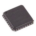
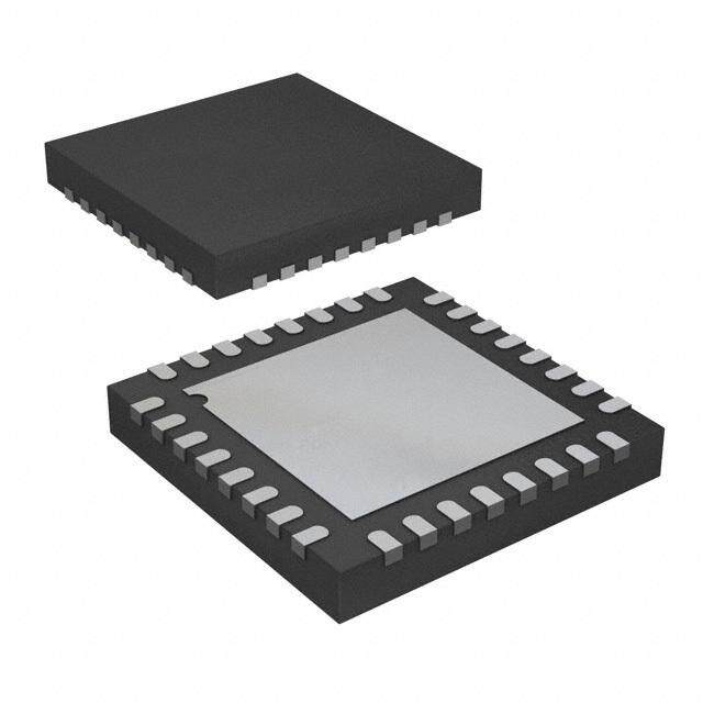
| 供应商器件封装 | 32-LFCSP-VQ(5x5) |
| 其它名称 | ADRF6510ACPZ-R7CT |
| 功能 | 可编程滤波器,VGA |
| 包装 | 剪切带 (CT) |
| 商标 | Analog Devices |
| 安装风格 | SMD/SMT |
| 封装 | Reel |
| 封装/外壳 | 32-VFQFN 裸露焊盘,CSP |
| 封装/箱体 | LFCSP-32 |
| 工作电源电压 | 5.25 V |
| 工厂包装数量 | 1500 |
| 带宽 | 30 MHz |
| 标准包装 | 1 |
| 电源电流 | 258 mA |
| 系列 | ADRF6510 |
| 视频文件 | http://www.digikey.cn/classic/video.aspx?PlayerID=1364138032001&width=640&height=505&videoID=2245193150001http://www.digikey.cn/classic/video.aspx?PlayerID=1364138032001&width=640&height=505&videoID= 2474683260001 |
| 辅助属性 | - |
| 通道数量 | 2 Channel |
| 配用 | /product-detail/zh/ADRF6510-EVALZ/ADRF6510-EVALZ-ND/4866739 |
| 频率 | 1MHz ~ 30MHz |


- 商务部:美国ITC正式对集成电路等产品启动337调查
- 曝三星4nm工艺存在良率问题 高通将骁龙8 Gen1或转产台积电
- 太阳诱电将投资9.5亿元在常州建新厂生产MLCC 预计2023年完工
- 英特尔发布欧洲新工厂建设计划 深化IDM 2.0 战略
- 台积电先进制程称霸业界 有大客户加持明年业绩稳了
- 达到5530亿美元!SIA预计今年全球半导体销售额将创下新高
- 英特尔拟将自动驾驶子公司Mobileye上市 估值或超500亿美元
- 三星加码芯片和SET,合并消费电子和移动部门,撤换高东真等 CEO
- 三星电子宣布重大人事变动 还合并消费电子和移动部门
- 海关总署:前11个月进口集成电路产品价值2.52万亿元 增长14.8%


PDF Datasheet 数据手册内容提取
30 MHz Dual Programmable Filters and Variable Gain Amplifiers Data Sheet ADRF6510 FEATURES FUNCTIONAL BLOCK DIAGRAM Matched pair of programmable filters and VGAs ENBL INP1 INM1 VPS COM GNSWOFS1 VPS Continuous gain control range: −5 dB to +45 dB 6-pole filter VPSD OPP1 1 MHz to 30 MHz in 1 MHz steps, 0.5 dB corner frequency COMD OPM1 SPI programmable LE COM 6 dB front-end gain step IMD3: >55 dBc for 1.5 V p-p composite output CLK SPI ADRF6510 GAIN HD2, HD3: >60 dBc for 1.5 V p-p output DATA VOCM Differential input and output SDO COM Adjustable output common-mode voltage COM OPM2 Optional dc output offset correction Power-down feature VPS OPP2 ASiPngPlLe I5C VA sTuIpOpNlyS o peration COM INP2 INM2 VPS COM OFDS OFS2 VPS 09002-001 Figure 1. Baseband I/Q receivers Diversity receivers ADC drivers GENERAL DESCRIPTION The ADRF6510 is a matched pair of fully differential low noise The variable gain amplifiers that follow the filters provide 50 dB and low distortion programmable filters and variable gain ampli- of continuous gain control with a slope of 30 mV/dB. The output fiers (VGAs). Each channel is capable of rejecting large out-of- buffers provide a differential output impedance of 20 Ω that is band interferers while reliably boosting the wanted signal, thus capable of driving 1.5 V p-p into 1 kΩ loads. The output common- reducing the bandwidth and resolution requirements on the mode voltage defaults to VPS/2, but it can be programmed via the analog-to-digital converters (ADCs). The excellent matching VOCM pin. The built-in dc offset correction loop can be disabled between channels and their high spurious-free dynamic range if dc-coupled operation is desired. The high-pass corner frequency over all gain and bandwidth settings makes the ADRF6510 is defined by external capacitors on the OFS1 and OFS2 pins. ideal for quadrature-based (IQ) communication systems with The ADRF6510 operates from a 4.75 V to 5.25 V supply and dense constellations, multiple carriers, and nearby interferers. consumes a maximum supply current of 258 mA when pro- The filters provide a six-pole Butterworth response with 0.5 dB grammed to the highest bandwidth setting. When disabled, it corner frequencies programmable through the SPI port from consumes 2 mA. The ADRF6510 is fabricated in an advanced 1 MHz to 30 MHz in 1 MHz steps. The preamplifier that precedes silicon-germanium BiCMOS process and is available in a the filters offers a pin-programmable option of either 6 dB or 32-lead, exposed paddle LFCSP. Performance is specified over 12 dB of gain. The preamplifier sets a differential input imped- the −40°C to +85°C temperature range. ance of 400 Ω and has a common-mode voltage that defaults to 2.1 V but can be driven from 1.5 V to 2.5 V. Rev. B Document Feedback Information furnished by Analog Devices is believed to be accurate and reliable. However, no responsibility is assumed by Analog Devices for its use, nor for any infringements of patents or other One Technology Way, P.O. Box 9106, Norwood, MA 02062-9106, U.S.A. rights of third parties that may result from its use. Specifications subject to change without notice. No license is granted by implication or otherwise under any patent or patent rights of Analog Devices. Tel: 781.329.4700 ©2010-2017 Analog Devices, Inc. All rights reserved. Trademarks and registered trademarks are the property of their respective owners. Technical Support www.analog.com
ADRF6510 Data Sheet TABLE OF CONTENTS Features .............................................................................................. 1 Distortion Characteristics ......................................................... 18 Applications ....................................................................................... 1 Maximizing the Dynamic Range ............................................. 18 Functional Block Diagram .............................................................. 1 Key Parameters for Quadrature-Based Receivers .................. 19 General Description ......................................................................... 1 Applications Information .............................................................. 20 Revision History ............................................................................... 2 Basic Connections ...................................................................... 20 Specifications ..................................................................................... 3 Error Vector Magnitude (EVM) Performance ........................... 20 Timing Diagrams .......................................................................... 5 EVM ............................................................................................. 21 Absolute Maximum Ratings ............................................................ 6 Effect of Filter Bandwidth on EVM ......................................... 21 ESD Caution .................................................................................. 6 Effect of Output Voltage Levels on EVM ................................ 21 Pin Configuration and Function Descriptions ............................. 7 Effect of C on EVM ............................................................... 22 OFS Typical Performance Characteristics ............................................. 8 Anti-Aliasing Filter .................................................................... 22 Theory of Operation ...................................................................... 15 Evaluation Board ............................................................................ 24 Input Buffers ............................................................................... 15 Evaluation Board Control Software ......................................... 24 Programmable Filters ................................................................. 15 Schematics and Artwork ........................................................... 24 Variable Gain Amplifiers (VGAs) ............................................ 16 Evaluation Board Configuration Options ............................... 27 Output Buffers/ADC Drivers ................................................... 16 Outline Dimensions ....................................................................... 29 DC Offset Compensation Loop ................................................ 16 Ordering Guide .......................................................................... 29 Programming the Filters ............................................................ 17 Noise Characteristics ................................................................. 17 REVISION HISTORY 9/2017—Rev. A to Rev. B Added EVM Section, Effect of Filter Bandwidth on EVM Changed CP-32-2 to CP-32-7 ...................................... Throughout Section, Effect of Output Voltage Levels on EVM Section, and Updated Outline Dimensions ....................................................... 29 Effect of C on EVM Section...................................................... 21 OFS Changes to Ordering Guide .......................................................... 29 Added Anti-Aliasing Filter Section .............................................. 22 Changes to Figure 54 ...................................................................... 22 10/2011—Rev. 0 to Rev. A Changes to Figure 58 ...................................................................... 24 Changes to Figure 2 and Figure 3 ................................................... 5 Changes to Figure 61 ...................................................................... 25 Changes to Table 3 ............................................................................ 7 Changes to Figure 62 and Figure 63 ............................................ 26 Changes to Figure 48, Changes to Error Vector Magnitude Changes to Table 5 .......................................................................... 27 (EVM) Performance Section ......................................................... 20 Deleted Low IF Image Rejection Section, and Example 4/2010—Revision 0: Initial Version Baseband Interface Section, Figure 50, and Figure 51; Renumbered Subsequent Figures ................................................. 20 Changes to Figure 49 ...................................................................... 21 Rev. B | Page 2 of 32
Data Sheet ADRF6510 SPECIFICATIONS VPS = 5 V, T = 25°C, Z = 400 Ω, Z = 1 kΩ, V = 1.5 V p-p, bandwidth setting = 30 MHz, GNSW = 0 V, unless otherwise noted. A SOURCE LOAD OUT Table 1. Parameter Test Conditions/Comments Min Typ Max Unit FREQUENCY RESPONSE Low-Pass Corner Frequency, f Six-pole Butterworth filter, 0.5 dB bandwidth 1 30 MHz C Step Size 1 MHz Corner Frequency Absolute Over operating temperature range ±15 % f C Accuracy Corner Frequency Matching Channel A and Channel B at same gain and ±0.5 % f C bandwidth settings Pass-Band Ripple 0.5 dB p-p Gain Matching Channel A and Channel B at same gain and ±0.1 dB bandwidth settings Group Delay Variation From midband to peak Corner Frequency = 1 MHz 135 ns Corner Frequency = 30 MHz 11 ns Group Delay Matching Channel A and Channel B at same gain Corner Frequency = 1 MHz 5 ns Corner Frequency = 30 MHz 0.2 ns Stop-Band Rejection Relative to Pass Band 2 × f 30 dB C 5 × f 75 dB C INPUT STAGE INP1, INM1, INP2, INM2 Maximum Input Swing At minimum gain, V = 0 V 1 V p-p GAIN Differential Input Impedance 400 Ω Input Common-Mode Range 1 V p-p input voltage 1.5 VPS/2 V Input pins left floating VPS/2 V GAIN CONTROL GAIN, GNSW Voltage Gain Range GNSW = 0 V, V from 0 V to 2 V −5 +45 dB GAIN GNSW = 5 V 1 51 dB Gain Slope 30 mV/dB Gain Error V from 500 mV to 1.7 V 0.2 dB GAIN Gain Step GNSW = 0 V to 5 V 6 dB OUTPUT STAGE OPP1, OPM1, OPP2, OPM2, VOCM Maximum Output Swing At maximum gain, R = 1 kΩ 2 V p-p LOAD HD2 > 60 dBc, HD3 > 60 dBc 1.5 V p-p Differential Output Impedance 20 Ω Output DC Offset Inputs shorted, offset loop disabled 35 mV Output Common-Mode Range 1.5 V p-p output voltage 1.5 3.0 V VOCM left floating VPS/2 V NOISE/DISTORTION 1 MHz Corner Frequency Output Noise Density Gain = 0 dB at f /2 −129 dBV/√Hz C Gain = 20 dB at f /2 −127 dBV/√Hz C Gain = 40 dB at f /2 −111 dBV/√Hz C Second Harmonic, HD2 250 kHz fundamental, 1.5 V p-p output voltage Gain = 0 dB 46.2 dBc Gain = 40 dB 43.2 dBc Third Harmonic, HD3 250 kHz fundamental, 1.5 V p-p output voltage Gain = 0 dB 52.2 dBc Gain = 40 dB 51.2 dBc Rev. B | Page 3 of 32
ADRF6510 Data Sheet Parameter Test Conditions/Comments Min Typ Max Unit IMD3 f1 = 500 kHz, f2 = 550 kHz, 1.5 V p-p composite output voltage Gain = 5 dB 61 dBc Gain = 35 dB 57 dBc IMD3 with Input CW Blocker f1 = 500 kHz, f2 = 550 kHz, 1.5 V p-p composite 40 dBc output, gain = 5 dB; blocker at 5 MHz, 10 dBc relative to two-tone composite output voltage 30 MHz Corner Frequency Output Noise Density Midband, gain = 0 dB −130 dBV/√Hz Midband, gain = 20 dB −130 dBV/√Hz Midband, gain = 40 dB −123 dBV/√Hz Second Harmonic, HD2 8 MHz fundamental, 1.5 V p-p output voltage Gain = 0 dB 63 dBc Gain = 40 dB 84 dBc Third Harmonic, HD3 8 MHz fundamental, 1.5 V p-p output voltage Gain = 0 dB 54 dBc Gain = 40 dB 87 dBc IMD3 f1 = 15 MHz, f2 = 16 MHz, 1.5 V p-p composite output voltage Gain = 5 dB 59 dBc Gain = 35 dB 77.5 dBc IMD3 with Input CW Blocker f1 = 15 MHz, f2 = 16 MHz, 1.5 V p-p composite 55 dBc output, gain = 5 dB; blocker at 150 MHz, 10 dBc relative to two-tone composite output voltage DIGITAL LOGIC LE, CLK, DATA, SDO, OFDS, GNSW Input High Voltage, V >2 V INH Input Low Voltage, V <0.8 V INL Input Current, I /I <1 µA INH INL Input Capacitance, C 2 pF IN SPI TIMING LE, CLK, DATA, SDO f 1/t 20 MHz CLK CLK t DATA hold time 5 ns DH t DATA setup time 5 ns DS t LE hold time 5 ns LH t LE setup time 5 ns LS t CLK high pulse width 5 ns PW t CLK to SDO delay 5 ns D POWER AND ENABLE VPS, VPSD, COM, COMD, ENBL Supply Voltage Range 4.75 5.0 5.25 V Total Supply Current ENBL = 5 V Maximum bandwidth setting 258 mA Minimum bandwidth setting 131 mA Disable Current ENBL = 0 V 2 mA Disable Threshold 2.5 V Enable Response Time Delay following ENBL low-to-high transition 20 µs Disable Response Time Delay following ENBL high-to-low transition 300 ns Rev. B | Page 4 of 32
Data Sheet ADRF6510 TIMING DIAGRAMS tCLK tPW CLK tLS tLH LE tDS tDH DATA WRITE BIT LSB LSB + 1 MSB – 2 MSB – 1 MMSSBB - 2 N1.O TWRTHEEOEGSR IFDSIT RRESERTGE DIDSA TTINEATR BO. I FTTO HDREE ATD EAWRTRMAI ITPNEIEN OS O PWNEH RCEAOTTNHIOSENER,C TTUHHTEEIV PFEAI RRRSITST II NSB GIWT ERSDIHTGOINEUGSL DTOO FB OET HRAE LR COELAGODICCIN K1G.. TFHREO CMO TRHNEE IRN TFERRENQAULE NCCOYR NWEORR FDR BEIQT UISE NTCHYEN 09002-003 Figure 2. Write Mode Timing Diagram tD tCLK tPW CLK tLS LE tDS tDH DATA READ BIT DC DC DC DC DC SDO LSB LSB + 1 MSB – 2 MSB – 1 MSB NOTES 1. TRTHHEEEG IFSSIDTROESR TP. IDFNAO OTRAN A BC RIOTEN DASEDET COEUPRTEMIRVINAEE T SFIOA WNL,HL TIENHTGEH EEFRDIR GTSEHTSE B OPITAF S RTHTHO EISU C LWLDRO BICTEKIN .AG L TOOG OICR 0 R. TEHAED ICNOGR FNREORM F TRHEEQ UINETNECRYN WALO CROD RBNITE RIS F TRHEEQNU UEPNDCAYT WEDO RADT 09002-004 Figure 3. Read Mode Timing Diagram Rev. B | Page 5 of 32
ADRF6510 Data Sheet ABSOLUTE MAXIMUM RATINGS Table 2. Stresses at or above those listed under Absolute Maximum Parameter Rating Ratings may cause permanent damage to the product. This is a Supply Voltages, VPS, VPSD 5.25 V stress rating only; functional operation of the product at these ENBL, GNSW, OFDS, LE, CLK, DATA, SDO VPS + 0.6 V or any other conditions above those indicated in the operational INP1, INM1, INP2, INM2 VPS + 0.6 V, section of this specification is not implied. Operation beyond GND − 0.6 V the maximum operating conditions for extended periods may OPP1, OPM1, OPP2, OPM2 VPS + 0.6 V affect product reliability. OFS1, OFS2 VPS + 0.6 V ESD CAUTION GAIN VPS + 0.6 V Internal Power Dissipation 1.4 W θ (Exposed Pad Soldered to Board) 37.4°C/W JA Maximum Junction Temperature 150°C Operating Temperature Range −40°C to +85°C Storage Temperature Range −65°C to +150°C Lead Temperature (Soldering 60 sec) 300°C Rev. B | Page 6 of 32
Data Sheet ADRF6510 PIN CONFIGURATION AND FUNCTION DESCRIPTIONS LBNE1PNI1MNISPVMOCWSNG1SFOSPV 21098765 33322222 VPSD 1 24 OPP1 COMD 2 23 OPM1 LE 3 22 COM ADRF6510 CLK 4 21 GAIN DATA 5 TOP VIEW 20 VOCM (Not to Scale) SDO 6 19 COM COM 7 18 OPM2 VPS 8 17 OPP2 910111213141516 M22SMS2S OCPNIMNIPVOCDFOSFOPV N1.O CATO ELNOSNWE CIMTP TEHDEA ENXCPEO GSREODUPNADDDPALDE.TO 09002-002 Figure 4. Pin Configuration Table 3. Pin Function Descriptions Pin No. Mnemonic Description 1 VPSD Digital Positive Supply Voltage: 4.75 V to 5.25 V. 2 COMD Digital Common. Connect to external circuit common using the lowest possible impedance. 3 LE Latch Enable. SPI programming pin. CMOS levels: V < 0.8 V, V > 2 V. LOW HIGH 4 CLK SPI Port Clock. CMOS levels: V < 0.8 V, V > 2 V. LOW HIGH 5 DATA SPI Data Input. CMOS levels: V < 0.8 V, V > 2 V. LOW HIGH 6 SDO SPI Data Output. CMOS levels: V < 0.8 V, V > 2 V. LOW HIGH 7, 9, 13, 19, 22, 28 COM Analog Common. Connect to external circuit common. 8, 12, 16, 25, 29 VPS Analog Positive Supply Voltage: 4.75 V to 5.25 V. 10, 11, 30, 31 INP2, INM2, Differential Inputs. 400 Ω input impedance. Common-mode range is 1.5 V to 2.5 V; default is 2.1 V. INM1, INP1 14 OFDS Offset Correction Loop Disable. Pull high to disable the offset correction loop. 15, 26 OFS2, OFS1 Offset Correction Loop Compensation Capacitors. Connect capacitors to circuit common. 17, 18, 23, 24 OPP2, OPM2, Differential Outputs. 20 Ω output impedance. Common-mode range is 1.5 V to 3 V; default is VPS/2. OPM1, OPP1 20 VOCM Output Common-Mode Setpoint. Defaults to VPS/2 if left open. 21 GAIN Analog Gain Control. 0 V to 2 V, 30 mV/dB gain scaling. 27 GNSW Front-End Gain Switch, 6 dB or 12 dB. Pull low for 6 dB; pull high for 12 dB. 32 ENBL Chip Enable. Pull high to enable. EP Exposed Paddle. Connect the exposed paddle to a low impedance ground pad. Rev. B | Page 7 of 32
ADRF6510 Data Sheet TYPICAL PERFORMANCE CHARACTERISTICS VPS = 5 V, T = 25°C, Z = 400 Ω, Z = 1 kΩ, V = 1.5 V p-p, GNSW = 0 V, unless otherwise noted. A SOURCE LOAD OUT 50 3.0 45 BANDWIDTH = 30MHz 2.5 BANDWIDTH = 30MHz +25°C 40 VPS = 4.75V, 5V, 5.25V 2.0 +85°C 35 1.5 VPS = 4.25V, 5V, 5.25V 30 B) 1.0 d B) 25 R ( 0.5 d O GAIN ( 2105 V–P4S0° =C 4.75V, 5V, 5.25V N ERR –0.50 +85°C AI 10 VPS = 4.75V, 5V, 5.25V G –1.0 +25°C VPS = 4.25V, 5V, 5.25V 5 –1.5 –40°C VPS = 4.25V, 5V, 5.25V 0 –2.0 –5 –2.5 –100 200 400 600 800 V10G0A0IN 1(2m0V0)1400 16001800 2000 2200 09002-005 –3.00 200 400 600 800 10V00GA1I2N0(0m1V4)0016001800200022002400 09002-008 Figure 5. In-Band Gain vs. VGAIN over Supply and Temperature Figure 8. Gain Conformance vs. VGAIN over Supply and Temperature (Bandwidth Setting = 30 MHz) (Bandwidth Setting = 30 MHz) 50 5 9 45 BANDWIDTH = 30MHz BANDWIDTH = 30MHz 40 35 3 8 30 25 PREAMP GAIN = 12dB 20 1 7 GAIN (dB) ––11–115050505 GAIN ERROR (dB) ––13 PREAMP GAIN = 6dB 65 GAIN STEP (dB) –20 –5 4 –25 –30 –35 –7 3 –40 –45 –501 FREQUE1N0CY (MHz) 100 09002-006 –90 5 10 F1R5EQUEN20CY (MH25z) 30 35 402 09002-009 Figure 6. Gain vs. Frequency by VGAIN (Bandwidth Setting = 30 MHz) Figure 9. 6 dB Gain Step and Gain Error vs. Frequency (Bandwidth Setting = 30 MHz, VGAIN = 0 V) 0.25 15 BANDWIDTH = 30MHz PREAMP GAIN = 6dB PREAMP GAIN = 12dB 0.20 10 B) MISMATCH (d 00..1150 dB (dBV rms) 50 N P1 AI 0.05 O –5 G 0 –10 –0.050 0.2 0.4 0.6 0.8 V1.G0AIN 1(.V2) 1.4 1.6 1.8 2.0 2.2 09002-007 –150 5 10 15 GAI2N0 (dB) 25 30 35 40 09002-010 Figure 7. Gain Matching vs. VGAIN (Bandwidth Setting = 30 MHz) Figure 10. Output P1dB vs. GAIN at 15 MHz (Bandwidth Setting = 30 MHz) Rev. B | Page 8 of 32
Data Sheet ADRF6510 40 1000 GAIN = 20dB 35 900 30 800 BW = 1MHz 25 s) 700 n B) 20 AY ( 600 N (d 15 DEL 500 AI P G 10 OU 400 R BW = 5MHz 5 G 300 BW = 10MHz 0 200 BW = 20MHz BW = 30MHz –5 100 –101M FREQU1E0NMCY (Hz) 100M 09002-011 00.5 FREQUEN5CY (MHz) 50 09002-014 Figure 11. Frequency Response vs. Bandwidth Setting (Gain = 30 dB), Figure 14. Group Delay vs. Frequency (Gain = 20 dB) Log Scale 32 1.0 BANDWIDTH = 30MHz 31 s) G (n 0.5 N HI GAIN = 20dB AIN (dB) 30 AY MATC 0 G 29 EL D P GAIN = 40dB U RO –0.5 28 G 271 6 11 F1R6EQUE2N1CY (MH26z) 31 36 40 09002-012 –1.00.5 FREQUENCY 5(MHz) 30 09002-015 Figure 12. Frequency Response vs. Bandwidth Setting (Gain = 30 dB), Figure 15. Group Delay Mismatch vs. Frequency Linear Scale (Bandwidth Setting = 30 MHz) 30 5 29 –40°C 4 BANDWIDTH = 1MHz 28 27 +25°C ns) 3 GAIN = 20dB 26 G ( N 2 25 HI C AIN (dB) 222234 +85°C LAY MAT 10 G 21 DE –1 GAIN = 0dB 20 UP O –2 19 R G 18 Q –3 I 17 –4 16 152 4 6 8 101214F1R6E1Q8U2E0N2C2Y 2(M4H2z6)28303234363840 09002-013 –50.2 0.4 0.6FREQUE0N.8CY (MHz)1.0 1.2 1.4 09002-016 Figure 13. Frequency Response over Temperature Figure 16. IQ Group Delay Mismatch vs. Frequency (Gain = 26 dB, Bandwidth Setting = 30 MHz) (Bandwidth Setting = 1 MHz) Rev. B | Page 9 of 32
ADRF6510 Data Sheet FREQUENCY (MHz) 100 0 0.5 1.0 1.5 2.0 2.5 3.0 0.75 90 0.50 dB) BANDWIDTH = 1MHz Bc) 80 TCH ( 0.25 BANDWIDTH = 30MHz Hz (d A M 70 UDE MISM 0 HD3 @ 24 60 ++++22285555°°°°CCCC,,,, VVVVPPPPSSSS==== 4545...V727555VVV PLIT–0.25 ++8855°°CC,, VVPPSS== 55.V25V AM 50 –40°C, VPS= 4.75V Q –40°C, VPS= 5V I–0.50 –40°C, VPS= 5.25V –0.750 5 10FREQUE1N5CY (MHz)20 25 30 09002-017 400 5 10 15 GAIN20 (dB) 25 30 35 40 09002-020 Figure 17. IQ Amplitude Mismatch vs. Frequency Figure 20. HD3 vs. Gain over Supply and Temperature (Bandwidth Setting = 30 MHz) 90 100 85 1.5V p-p OUTPUT @ 8MHz BANDWIDTH = 30MHz 90 80 75 c) c) 80 B B d 70 d Hz ( Hz ( M 65 M 70 16 +25°C, VPS= 4.75V 24 @ 60 +25°C, VPS= 5V @ 2 +25°C, VPS= 5.25V 3 D D 60 H 55 +85°C, VPS= 4.75V H +85°C, VPS= 5V 50 +85°C, VPS= 5.25V VOCM = 1.5V –40°C, VPS= 4.75V 50 VOCM = 1.75V 45 –40°C, VPS= 5V VOCM = 2V –40°C, VPS= 5.25V VOCM = 2.5V 400 5 10 15 GAIN20 (dB) 25 30 35 40 09002-018 400 5 10 15 GAIN20 (dB) 25 30 35 40 09002-021 Figure 18. HD2 vs. Gain over Supply and Temperature Figure 21. HD3 vs. Gain over Output Common-Mode Voltage (Bandwidth Setting = 30 MHz) (Bandwidth Setting = 30 MHz) 100 30 1.5V p-p OUTPUT @ 8MHz BANDWIDTH = 30MHz BANDWIDTH = 30MHz f1 = 14MHz, f2 = 15MHz 90 25 PREAMP 80 GAIN = 6dB c) 20 B @ 16MHz (d 6700 OIP3 (dBV) 15 PREAMP 2 GAIN = 12dB D 10 H 50 VOCM = 1.5V VOCM = 1.75V 5 40 VOCM = 2V VOCM = 2.5V 300 5 10 15 GAIN20 (dB) 25 30 35 40 09002-019 00 5 10 15 20GAIN25 (dB)30 35 40 45 50 09002-022 Figure 19. HD2 vs. Gain over Output Common-Mode Voltage Figure 22. In-Band OIP3 vs. Gain (Bandwidth Setting = 30 MHz) (Bandwidth Setting = 30 MHz) Rev. B | Page 10 of 32
Data Sheet ADRF6510 30 65 BANDWIDTH = 30MHz 4555 BANDWIDTH = 30MHz f1 = 14MHz, f2 = 15MHz 35 25 25 –40°C 15 +25°C 5 20 +85°C dBV) –1–55 2:1 SLOPE OIP3 (dBV) 15 @ 15MHz ( ––––54325555 GAPIRNE =A M12PdB 2 –65 OUT-OF-BAND IIP2 10 MD –75 I –85 –95 –105 PREAMP 5 GAIN = 6dB –115 –125 –135 00 5 10 15 GAIN20 (dB) 25 30 35 40 09002-023 –145–45 –35INP–U2T5 LE–V15EL @–5 115M5Hz AN15D 1302M5Hz 3(d5BV/T4o5ne)55 65 09002-060 Figure 23. In-Band OIP3 vs. Gain over Temperature Figure 26. Out-of-Band IIP2: IMD2 Tone at Midband (Preamp Gain = 6 dB, Bandwidth Setting = 30 MHz) (Bandwidth Setting = 30 MHz) 120 10 GAIN = 0dB 0 BANDWIDTH = 30MHz GAIN = 10dB 100 GAIN = 20dB –10 GAIN = 30dB –20 GAIN = 40dB –30 80 V) dB –40 3:1 SLOPE Bc) Hz ( –50 MD3 (d 60 @ 15M ––7600 GAPIRNE =A M12PdB I 40 MD3 –80 OUT-OF-BAND IIP3 I –90 –100 PREAMP 20 GAIN = 6dB –110 –120 0 –130 0 0.5 CO1M.0POSIT1E.5 OUTP2U.0T VOL2T.5AGE (3V. 0p-p) 3.5 4.0 09002-024 –45 –4I0NPU–T3 5LEV–E3L0 @ –12155MH–z2 A0ND– 21155MH–1z0 (dBV–/5Tone)0 5 09002-027 Figure 24. In-Band Third-Order Intermodulation Distortion Figure 27. Out-of-Band IIP3: IMD3 Tone at Midband (Preamp Gain = 6 dB, Bandwidth Setting = 30 MHz) (Bandwidth Setting = 30 MHz) 120 70 GAIN = 6dB 1MHz BW GAIN = 16dB 65 2MHz BW 100 GAIN = 26dB 4MHz BW GAIN = 36dB 60 6MHz BW GAIN = 46dB Ω) 8MHz BW 0 55 80 e 5 30MHz BW D3 (dBc) 60 URE (dB r 5405 IM FIG 40 40 E OIS 35 N 30 20 25 00 0.5 CO1M.0POSIT1E.5 OUTP2U.0T VOL2T.5AGE (3V. 0p-p) 3.5 4.0 09002-025 20–5 0 5 10 15GAIN20 (dB)25 30 35 40 45 09002-028 Figure 25. In-Band Third-Order Intermodulation Distortion Figure 28. Noise Figure vs. Gain over Bandwidth Setting, (Preamp Gain = 12 dB, Bandwidth Setting = 30 MHz) Preamp Gain = 6 dB (Noise Figure at 1/2 Bandwidth) Rev. B | Page 11 of 32
ADRF6510 Data Sheet 60 –90 55 1MHz BW –95 GAIN = 0dB 2MHz BW GAIN = 20dB B re 50Ω) 544050 4683MMM0MHHHHzzz zBBB BWWWW V rms/√Hz) –––111001050 GAIN = 40dB d B RE ( 35 E (d –115 U S G OI FI 30 N –120 E T NOIS 25 UTPU –125 20 O –130 15 –135 100 5 10 15 20GAIN25 (dB)30 35 40 45 50 09002-029 –1400.5 1.0 FR1E.5QUENCY (M2.H0z) 2.5 3.0 09002-032 Figure 29. Noise Figure vs. Gain over Bandwidth Setting, Figure 32. Output Noise Density vs. Frequency (Bandwidth Setting = 1 MHz) Preamp Gain = 12 dB (Noise Figure at 1/2 Bandwidth) –100 –110 1MHz BW GAIN = 0dB –105 2MHz BW GAIN = 20dB 4MHz BW –115 GAIN = 40dB Hz) 6MHz BW Hz) ms/√ –110 83M0MHHz zB BWW ms/√ –120 V r V r B –115 B d d E ( E ( –125 S S OI –120 OI N N UT UT –130 TP –125 TP U U O O –130 –135 –135–5 0 5 10 15GAIN20 (dB)25 30 35 40 45 09002-030 –14010 12 14 16 FR1E8QUE2N0CY (M22Hz) 24 26 28 30 09002-033 Figure 30. Output Noise Density vs. Gain by Bandwidth Setting, Figure 33. Output Noise Density vs. Frequency (Bandwidth Setting = 20 MHz) Preamp Gain = 6 dB (Noise at 1/2 Bandwidth) –100 –90 1MHz BW –95 BV rms/√Hz) –––111011505 24683MMMM0MHHHHHzzzz zBBBB BWWWWW MHz (dBV/√Hz) –––111100050 GAIN = 40dB E (d @ 15 –115 TPUT NOIS ––112205 UT NOISE ––112250 GAIN = 20dB U P O UT –130 GAIN = 0dB –130 O –135 –1350 5 10 15 20GAIN25 (dB)30 35 40 45 50 09002-031 –140–35 –B30LOCKER L–E2V5EL @ 150–M2H0z (dBV rm–s1)5 –10 09002-034 Figure 31. Output Noise Density vs. Gain by Bandwidth Setting, Figure 34. Output Noise Density vs. Blocker Level Preamp Gain = 12 dB (Noise at 1/2 Bandwidth) (Bandwidth Setting = 30 MHz, Blocker at 150 MHz) Rev. B | Page 12 of 32
Data Sheet ADRF6510 450 10 280 440 5 260 430 0 240 420 –5 220 410 –10 A) R (Ω)IN 400 –15 C (pF)IN (mPPLY 210800 390 –20 SU I 160 380 –25 140 370 –30 360 –35 120 3500 5 10FREQUE1N5CY (MHz)20 25 30–40 09002-035 1000 5 BA1N0DWIDTH 1S5ETTING (2M0Hz) 25 30 09002-038 Figure 35. Input Impedance vs. Frequency (Bandwidth Setting = 30 MHz) Figure 38. Current Consumption vs. Bandwidth Setting (Gain = 20 dB) 28 200 266 27 100 264 262 26 0 R(Ω)SERIES_OUT 222543 –––123000000 (nH)LSERIES_OUT I (mA)SUPPLY 222255564680 22 –400 252 VPS = 4.75V 21 –500 250 VVPPSS == 55.V25V 200 5 10FREQUE1N5CY (MHz)20 25 30–600 09002-036 248–50 –30 –10 TEMP10ERATUR3E0 (°C) 50 70 90 09002-039 Figure 36. Output Impedance vs. Frequency (Bandwidth Setting = 30 MHz) Figure 39. Current Consumption vs. Temperature over Supply (Bandwidth Setting = 30 MHz) 90 70 BANDWIDTH = 30MHz BANDWIDTH = 30MHz 80 60 GAIN = 40dB 70 GAIN = 40dB 50 B) 60 GAIN = 20dB N (d 50 dB) 40 OLATIO 40 GAIN = 20dB CMRR ( 30 IS 30 GAIN = 0dB 20 20 10 10 00.1 1FREQUENCY (MHz)10 100 09002-037 00 5 10FREQUE1N5CY (MHz)20 25 30 09002-040 Figure 37. Channel Isolation, Output to Output, vs. Frequency Figure 40. Common-Mode Rejection Ratio vs. Frequency (Bandwidth Setting = 30 MHz) (Bandwidth Setting = 30 MHz) Rev. B | Page 13 of 32
ADRF6510 Data Sheet 302M8MHHz zB MAANIDNWTOIDNTEH, VGAIN = 1400mV TO 800mV INPUT SIGNAL = 45mV p-p OUTPUT SIGNAL = 450mV p-p 28MHz SIGNAL = 45mV p-p 20dB OF GAIN TO 450mV p-p 400nsV/GDAIVIN = 800mV TO 1.40V 09002-067 Figure 41. Gain Step Response Rev. B | Page 14 of 32
Data Sheet ADRF6510 THEORY OF OPERATION The ADRF6510 consists of a matched pair of buffered, program- band rejection, ripple, and group delay. The 0.5 dB bandwidth is mable filters followed by variable gain amplifiers and output programmed from 1 MHz to 30 MHz in 1 MHz steps via the serial ADC drivers. The block diagram of a single channel is shown programming interface (SPI) as described in the Programming in Figure 42. The programmability of the bandwidth and of the the Filters section. pre- and post-filtering gain offers great flexibility when coping The filters are designed so that the Butterworth prototype filter with signals of varying levels in the presence of noise and large, shape and group delay responses vs. frequency are retained for undesired signals nearby. The entire differential signal chain is any bandwidth setting. Figure 43 and Figure 44 illustrate the dc-coupled with flexible interfaces at the input and output. The ideal six-pole Butterworth gain and group delay responses, bandwidth and gain setting controls for the two channels are respectively. The group delay, τ, is defined as g shared, ensuring close matching of their magnitude and phase τ = −∂φ/∂ω responses. The ADRF6510 can be fully disabled through the g ENBL pin. where: φ is the phase in radians. 6dB/12dB 1MHz TO 30MHz 50dB OUTPUT ADC PREAMP PROG. FILTERS VGA DRIVER ω = 2πf is the frequency in radians/second. BASIENBPAUNTDS BOAUSTEPBUATSND Note that for a frequency scaled filter prototype, the absolute magnitude of the group delay scales inversely with the band- width; however, the shape is retained. For example, the peak SPI INTERFACE group delay for a 28 MHz bandwidth setting is 14× less than PREAMP GAIANN CAOLNOTGROL OUTPUT for a 2 MHz setting. GAIN SWITCH 30mV/dB COMMON-MODE PROSGFPIRLI ATBEMURMSING CONTROL 09002-042 –200 Figure 42. Signal Path Block Diagram for a Single Channel of the ADRF6510 Filtering and amplification are fundamental operations in any Hz) –40 signal processing system. Filtering is necessary to select the DE ( –60 U intended signal while rejecting out-of-band noise and interferers. NIT –80 G Amplification increases the level of the desired signal to overcome A M –100 noise added by the system. When used together, filtering and E V amplification can extract a low level signal of interest in the ATI –120 L presence of noise and out-of-band interferers. Such analog RE –140 signal processing alleviates the requirements on the analog, –160 mixed signal, and digital components that follow. INPUT BUFFERS –1801M 10MFREQUENCY (Hz1)00M 1G 09002-043 The input buffers provide a convenient interface to the sensitive Figure 43. Sixth-Order Butterworth Magnitude Response for 0.5 dB filter sections that follow. They set a differential input impedance Bandwidths; Programmed from 2 MHz to 29 MHz in 1 MHz Steps of 400 Ω and sit at a nominal common-mode voltage of VPS/2. 500 The inputs can be dc-coupled or ac-coupled. If using direct dc-coupling, the common-mode voltage, VCM, can range from 400 1.5 V to 3 V. A current flows into or out of the input pins to 2MHz 28MHz accommodate the difference in common-mode voltages. The s) 300 n current into each pin is given by Y ( A L (VCM – (VPS/2))/200 Ω P DE 200 14x U The input buffers in both channels can be configured simulta- O neously to a gain of 6 dB or 12 dB through the GNSW pin. When GR 100 configured for a 6 dB gain, the buffers support up to a 1 V p-p 0 differential input level with >50 dBc harmonic distortion. For a 12 dB gain setting, the buffers support 0.5 V p-p inputs. PROGRAMMABLE FILTERS –101000k 1MFREQUENCY (Hz)10M 100M 09002-044 The integrated programmable filter is the key signal processing Figure 44. Sixth-Order Butterworth Group Delay Response for function in the ADRF6510. The filters follow a six-pole Butter- 0.5 dB Bandwidths; Programmed to 2 MHz and 28 MHz worth prototype response that provides a compromise between Rev. B | Page 15 of 32
ADRF6510 Data Sheet The corner frequency of the filters is defined by RC products, DC OFFSET COMPENSATION LOOP which can vary by ±30% in a typical process. Therefore, all the In many signal processing applications, no information is parts are factory calibrated for corner frequency, resulting in carried in the dc level. In fact, dc voltages and other low a residual ±10% corner frequency variation over the −40°C to frequency disturbances can often dominate the intended signal +85°C temperature range. Although absolute accuracy requires and consume precious dynamic range in the analog path and calibration, the matching of RC products between the pair of bits in the data converters. These dc voltages can be present channels is better than 1% by observing careful design and with the desired input signal or can be generated inside the layout practices. Calibration and excellent matching ensure signal path by inherent dc offsets or other unintended signal- that the magnitude and group delay responses of both channels dependent processes such as self-mixing or rectification. track together, a critical requirement for digital IQ-based Because the ADRF6510 is fully dc-coupled, it may be necessary communication systems. to remove these offsets to realize the maximum signal-to-noise VARIABLE GAIN AMPLIFIERS (VGAs) ratio (SNR). This can be achieved with ac-coupling capacitors The VGAs are implemented using the Analog Devices, Inc., at the input and output pins, but that requires large values patented X-AMP® architecture, consisting of a tapped 50 dB because the impedances are fairly low, and high-pass corners attenuator followed by a fixed-gain amplifier. The X-AMP archi- may need to be <10 Hz in some cases. To address the issue of dc tecture generates a linear-in-dB monotonic gain response with offsets, the ADRF6510 provides an offset correction loop that low ripple. The gain is controlled through the high impedance nulls the output differential dc level as shown in Figure 46. If GAIN pin with an accurate slope of 30 mV/dB. The gain response the correction loop is not required, it can be disabled through shown in Figure 45 shows the GAIN pin voltage range and the the OFDS pin. absence of gain foldback at high V . GAIN 50 0.3 OFDS COFS OFSx 30mV/dB 40 0.2 30 0.1 B) dB) OR (d FILFTREORMS BOAUSTEPBUATND AIN ( 20 0 ERR 50dB OUTPUT ADC G N VGA DRIVER 10 –0.1 GAI GAIN 09002-066 Figure 46. Offset Compensation Loop Operation around the VGA 0 –0.2 and Output Buffer The offset control loop creates a high-pass corner, f , that –100 0.5 1.0 1.5 VGA2I.N0 (V) 2.5 3.0 3.5 4.0–0.3 09002-045 iTsy spuipcaelrliym, fpo sies dm oann yth oer dneorrsm oaf lm Baugttneirtwudoer tlho wfieltre rth raeHnsPp tohnes leo.w er HP Figure 45. Linear-in-dB Gain Control Response of the X-AMP VGA programmed filter bandwidth so that there is no interaction Showing Consistent Slope and Low Error between them. Setting f is accomplished with capacitors, HP OUTPUT BUFFERS/ADC DRIVERS C , from the OFS1 and OFS2 pins to ground. Because the OFS correction loop works around the VGA section, f is also The low impedance (20 Ω) output buffers of the ADRF6510 are HP dependent on the gain of the VGA. In general, the expression designed to drive either ADC inputs or subsequent amplifier stages. for f is given by They are capable of delivering up to 4 V p-p composite two-tone HP signals into 500 Ω differential loads with >60 dBc IM3. The f (Hz) = 1.2 × (Gain/C ) HP OFS output common-mode voltage defaults to VPS/2, but it can be where: adjusted from 1.5 V to 3.0 V without loss of drive capability by Gain is expressed in linear terms, not in decibels (dB). presenting the VOCM pin with the desired common-mode C is expressed in microfarads (µF). OFS voltage. The high input impedance of VOCM allows the ADC Note that f increases in proportion to the gain. For this reference output to be connected directly. Even though the HP reason, C should be chosen at the highest operating gain signal path is fully dc-coupled and the dc offset compensation OFS to guarantee that f is always below the maximum limit loop can remove undesired dc offsets (see the DC Offset HP required by the system. Compensation Loop section), the output buffers can be ac- coupled to the next stage by properly selecting the coupling capacitors according to the load impedance. Rev. B | Page 16 of 32
Data Sheet ADRF6510 PROGRAMMING THE FILTERS NOISE CHARACTERISTICS The 0.5 dB corner frequencies for both filters are programmed The output noise behavior of the ADRF6510 depends on the gain simultaneously through the SPI port. A 5-bit register stores the and bandwidth settings. Both the filter sections and the VGAs codes for corner frequencies of 1 MHz through 30 MHz (see contribute to the total noise at the output. The filter contributes Table 4). The SPI protocol not only allows frequency codes to a noise spectral density profile that is flat at low frequencies, peaks be written to the DATA pin but also allows the stored code to near the corner frequency, and then rolls off as the filter poles be read back from the SDO pin. roll off the gain. The magnitude of the noise spectral density, expressed in nV/√Hz, varies inversely with the square root of The latch enable (LE) pin must first go to a Logic 0 for a read or the bandwidth setting, resulting in a total integrated noise in write cycle to begin. On the next rising edge of the clock (CLK), nV that is nearly constant with bandwidth setting. a Logic 1 on the DATA pin initiates a write cycle, whereas a Logic 0 on the DATA pin initiates a read cycle. In a write cycle, The X-AMP type VGAs used in the ADRF6510 contribute the next five CLK rising edges latch the frequency code, LSB a fixed noise spectral density to the output, independent of first. When LE goes high, the write cycle is completed and the the gain setting, of −130 dBV/√Hz, which is equivalent to frequency code is presented to the filter. In a read cycle, the next 316 nV/√Hz. Although the VGA noise contribution to the five CLK falling edges present the stored frequency code, LSB output is fixed, the gain of the VGA controls the relative first. When LE goes high, the read cycle is completed. Detailed contribution of the filter noise. timing diagrams are shown in Figure 2 and Figure 3. Figure 47 and Figure 48 show the total output noise spectral density vs. frequency for different bandwidth settings. At low Table 4. Frequency Code vs. Corner Frequency Lookup Table values of VGA gain, the noise at the output is the flat spectral 5-Bit Binary Frequency Code1 Corner Frequency (MHz) density contributed by the VGA because the filter noise is sup- 00000 1 pressed by the VGA attenuation. As the gain increases, more 00001 2 of the filter noise appears at the output. Because the filter noise 00010 3 increases at lower bandwidth settings, it overwhelms the VGA 00011 4 noise floor. In either case, the noise density asymptotically 00100 5 approaches the −130 dBV/√Hz limit set by the VGA at the 00101 6 highest frequencies. For other values of VGA gain and band- 00110 7 width setting, the detailed shape of the noise spectral density 00111 8 changes. 01000 9 01001 10 –115 BANDWIDTH = 20MHz 01010 11 01011 12 GAIN = 40dB 01100 13 Hz) –120 √ 01101 14 BV/ d 01110 15 E ( 01111 16 OIS –125 N 10000 17 UT P 10001 18 UT GAIN = 20dB O –130 10010 19 GAIN = 0dB 10011 20 10100 21 1100110110 2223 –13510 15 20 25 FR3E0QUE3N5CY (M40Hz) 45 50 55 60 09002-046 Figure 47. Total Output Noise with a 20 MHz Corner Frequency 10111 24 for Three Different Gain Settings 11000 25 11001 26 11010 27 11011 28 11100 29 11101 30 11110 30 11111 30 1 MSB first. Rev. B | Page 17 of 32
ADRF6510 Data Sheet –100 To distinguish and quantify the distortion performance of the BANDWIDTH = 1MHz input section, two different IP3 specifications are presented. –105 The first is called in-band IP3 and refers to a two-tone test GAIN = 40dB Hz) –110 where the signals are inside the filter bandwidth. This is exactly √ V/ the same figure of merit familiar to communications engineers B E (d –115 in which the third-order intermodulation level, IM3, is S OI measured. T N –120 U GAIN = 20dB To quantify the effect of out-of-band signals, a new out-of-band P T U –125 (OOB) IIP3 figure of merit is introduced. This test also involves O a two-tone stimulus; however, the two tones are placed out-of- –130 band so that the lower IM3 product lands in the middle of the GAIN = 0dB filter pass band. At the output, only the IM3 product is visible –1350.5 1.0 FR1E.5QUENCY (M2.H0z) 2.5 3.0 09002-047 bOeOcaBu IsPe 3th aet othreig iinnpaul ttw, toh eto InMes3 alerev efli litse rreedfe orruetd. Ttoo tchaelc iunlpautet tbhye Figure 48. Total Output Noise with a 1 MHz Corner Frequency the overall gain. The OOB IIP3 allows the user to predict the for Three Different Gain Settings impact of out-of-band blockers or interferers at an arbitrary Note that the noise spectral density outside the filter bandwidth signal level on the in-band performance. The ratio of the is limited by the fixed VGA output noise. It may be necessary to desired input signal level to the input-referred IM3 at a given use an external, fixed-frequency, passive filter prior to an analog- blocker level represents a signal-to-distortion limit imposed by to-digital conversion to prevent noise aliasing from degrading the out-of-band signals. the signal-to-noise ratio. The higher the sampling rate relative MAXIMIZING THE DYNAMIC RANGE to the maximum ADRF6510 corner frequency setting to be used, the lower the order of the external filter. The role of the ADRF6510 is to increase the level of a variable DISTORTION CHARACTERISTICS in-band signal while minimizing out-of-band signals. Ideally, this is achieved without degrading the SNR of the incoming The distortion performance of the ADRF6510 is similar to its signal or introducing distortion to the incoming signal. noise performance. The filters and the VGAs contribute to the The first goal is to maximize the output signal swing, which can overall distortion and signal handling capabilities. Furthermore, be defined by the ADC input range or the input signal capacity the front end must also cope with out-of-band signals that can be of the next analog stage. For the complex waveforms often encoun- larger than the in-band signals. These out-of-band signals are tered in communication systems, the peak-to-average ratio, or filtered before reaching the VGA. It is important to understand crest factor, must be considered when choosing the peak-to-peak the signals presented to the ADRF6510 and to match these output. From the chosen output signal and the maximum gain signals with the input and output characteristics of the part. of the ADRF6510, the minimum input level can be defined. When the gain is low, the distortion is typically limited by the Lower signal levels do not yield the maximum output and suffer input section because the output is not driven to its maximum a greater degradation in SNR. capacity. When the gain is high, the distortion is likely limited As the input signal level increases, the VGA gain is reduced from by the output section because the input is not driven to its its maximum gain point to maintain the desired fixed output maximum capacity. An exception to this is when the input is level. The output noise, initially dominated by the filter, follows driven with a small desired signal in combination with a large the gain reduction, yielding a progressively better SNR. At some out-of-band signal. In this case, the out-of-band signal may point, the VGA gain drops sufficiently that the constant VGA drive the input to distort. As long as the input is not overdriven, noise becomes dominant, resulting in a constant SNR from that the out-of-band signal is removed by the filter. A high VGA point. From the perspective of SNR alone, the maximum input gain is still needed to raise the small desired signal to a higher level is reached when the VGA reaches its minimum gain. level at the output. The overall distortion introduced by the part depends on the input drive level, including the out-of-band Distortion must also be considered when maximizing the dynamic signals, and the desired output signal level. range. At low and moderate signal levels, the output distortion is constant and assumed to be adequate for the selected output As noted in the Input Buffers section, the input section can level. At some point, the input signal becomes large enough that handle a total signal level of 1 V p-p for a 6 dB preamplifier and distortion at the input limits the system. The maximum tolerable 500 mV p-p for a 12 dB preamplifier with >50 dBc harmonic input signal depends on whether the input distortion becomes distortion. This includes both in-band and out-of-band signals. unacceptably large or the minimum gain is reached. Rev. B | Page 18 of 32
Data Sheet ADRF6510 The most challenging scenario in terms of dynamic range is the and quadrature (Q) sinusoidal carriers. Both the baseband and presence of a large out-of-band blocker accompanying a weaker modulated signals appear quite complex in the time domain with in-band wanted signal. In this case, the maximum input level is dramatic peaks and valleys. In a typical receiver, the goal is to dictated by the blocker and its inclination to cause distortion. recover the pair of quadrature baseband signals in the presence After filtering, the weak wanted signal must be amplified to the of noise and interfering signals after quadrature demodulation. desired output level, possibly requiring maximum gain. Both In the process of filtering out-of-band noise and unwanted inter- the distortion limits associated with the blocker at the input and ferers and restoring the levels of the wanted I and Q baseband the SNR limits created by the weaker signal and higher gains are signals, it is critical to retain their gain and phase integrity over present simultaneously. Furthermore, not only does the blocker the bandwidth. scenario degrade the dynamic range but it also reduces the The ADRF6510 delivers flat in-band gain and group delay, range of input signals that can be handled because a larger part consistent with a six-pole Butterworth prototype filter as of the gain range is used to simply extract the weak desired described in the Programmable Filters section. Furthermore, signal from the stronger blocker. careful design ensures excellent matching of these parameters KEY PARAMETERS FOR QUADRATURE-BASED between the I and Q channels. Although absolute gain flatness RECEIVERS and group delay can be corrected with digital equalization, mismatch introduces quadrature errors and intersymbol inter- The majority of digital communication receivers makes use of ference that degrade bit error rates in digital communication quadrature signaling, in which bits of information are encoded systems. onto pairs of baseband signals that then modulate in-phase (I) Rev. B | Page 19 of 32
ADRF6510 Data Sheet APPLICATIONS INFORMATION BASIC CONNECTIONS ERROR VECTOR MAGNITUDE (EVM) PERFORMANCE Figure 49 shows the basic connections for operating the Error vector magnitude (EVM) is a measure used to quantify ADRF6510. A voltage from 4.75 V to 5.25 V should be applied the performance of a digital radio transmitter or receiver by to the supply pins. Each supply pin should be decoupled with at measuring the fidelity of the digital signal transmitted or least one low inductance, surface-mount ceramic capacitor of received. Various imperfections in the link, such as magnitude 0.1 µF placed as close as possible to the device. and phase imbalance, noise, and distortion, cause the constel- lation points to deviate from their ideal locations. The input buffers provide an interface to the sensitive filter sections that follow. They set a differential input impedance In general, a receiver exhibits three distinct EVM limitations of 400 Ω and sit at a nominal common-mode voltage of VPS/2. vs. received input signal power. As signal power increases, the The inputs can be dc-coupled or ac-coupled. If using direct distortion components increase. dc-coupling, the common-mode voltage, V , can range from CM • At large enough signal levels, where the distortion compo- 1.5 V to 3 V. nents due to the harmonic nonlinearities in the device The output buffers of the ADRF6510 are low impedance dominate, EVM degrades as signal levels increase. (~20 Ω) designed to drive either ADC inputs or subsequent • At medium signal levels, where the signal chain behaves amplifier stages. The output common-mode voltage defaults to in a linear manner and the signal is well above any notable VPS/2 but can be adjusted from 1.5 V to 3.0 V without loss of noise contributions, EVM has a tendency to reach an drive capability by presenting the VOCM pin with the desired optimal level determined dominantly by either the common-mode voltage. The high input impedance of VOCM quadrature accuracy and I/Q gain match of the signal allows the ADC reference output to be connected directly. chain or the precision of the test equipment. To enable the ADRF6510, the ENBL pin must be pulled high. • As signal levels decrease, such that noise is a major con- Taking ENBL low disables the device, reducing current con- tributor, EVM performance vs. the signal level exhibits sumption to approximately 2 mA at ambient temperature. a decibel-for-decibel degradation with decreasing signal levels. At these lower signal levels, where noise is the dominant limitation, decibel EVM is directly proportional to the SNR. VPS VPS INM1 INP1 VPS VPS OPP1 ENBL INM1 COM OFS1 OPM1 INP1 VPS GNSW VPS VPSD VPSD OPP1 COMD OPM1 LE LE COM CLK CLK ADRF6510 GAIN VPS DATA DATA VOCM VPS SDO SDO COM COM OPM2 OPM2 VPS VPS OPP2 OPP2 INP2 VPS OFDS VPS COM INM2 COM OFS2 VPS INP2 VPS INM2 VPS 09002-050 Figure 49. Basic Connections Rev. B | Page 20 of 32
Data Sheet ADRF6510 EVM The basic setup to test EVM for the ADRF6510 consisted of an While low-pass filtering with the ADRF6510 to reject out-of- Agilent E4438C used as a RF signal source with an Agilent band undesired signals (blockers), more rejection of the InfiniiVision DSO7104B oscilloscope in conjunction with the undesired signals may be required. If the filter bandwidth is set Agilent 89600 VSA software to sample the signal and compute to approximately the same as the signal bandwidth, the user the EVM. The E4438C RF output drove the RF port of the may trade some degradation of EVM for a gain in rejection of ADL5380 IQ demodulater, which in turn drove the baseband the out-of-band undesired signals, by lowering the low-pass differential inputs of the ADRF6510. filter bandwidth corner (for example, by 1 MHz). The I and Q outputs of the ADRF6510 were taken differentially Lowering the filter bandwidth to gain more rejection works into two AD8130 difference amplifiers to convert them into progressively better the lower the signal and filter bandwidths single-ended signals. The single-ended signals were connected are set to (see Figure 43). A 1 MHz change from 3 MHz filter to the input channels of the oscilloscope, which captured the bandwidth to 2 MHz filter bandwidth yields about 20 dB more modulated waveforms. rejection. Compare that to a 1 MHz change from 29 MHz filter band-width to 28 MHz filter bandwidth, which will yield about An overall baseband EVM performance was measured on the 1 dB more in rejection. ADRF6510. A modulation setting of 4 QAM and, unless otherwise noted, a 5 MHz symbol rate were used, with a pulse Figure 51 shows that degradation of EVM as signal bandwidth shaping filter alpha of 0.35. The analog gain of the ADRF6510 (positive frequency only) is swept while keeping the filter was adjusted to maintain 1.5 V p-p into a 1 kΩ differential load bandwidth set to 5 MHz. Three different COFS capacitor values impedance. Figure 50 shows EVM vs. input power for three were used. different IF frequencies. The input power is the integrated input 0 FILTER BW CORNER power over the bandwidth of the modulated signal. –5 In Figure 50, the ADRF6510 shows excellent EVM of better than −-35 dB over a 50 dB range at a 0Hz IF. The user can –10 COFS = 1nF chose to use a complex IF of 5 MHz to achieve even a better –15 EVM of at least −40 dB over a 50 dB range. B) d M (–20 0 V E –5 –25 COFS = 100nF –10 –30 –15 –35 B)–20 COFS = 1µF EVM (d––2350 –400 2 4SIGNAL B6ANDWID8TH (MHz1)0 12 14 09002-151 2.5MHz IF Figure 51. EVM vs. Signal Bandwidth over COFS Values While Maintaining a –35 Filter Bandwidth of 5 MHz –40 0Hz IF EFFECT OF OUTPUT VOLTAGE LEVELS ON EVM –45 5MHz IF Output voltage level can affect EVM greatly when the signal –50–80 –70 –60 –50 –P4I0N (dB–m30) –20 –10 0 10 09002-058 the ADRFis6 c5o1m0,p tarekses ecda.r eW tchhaeaunts techshe aE oVnuMgti npduget gt shriaegd noaautlti poisun nt. ovto ilnta cgoem lepvreelsss oiofn , which Figure 50. EVM vs. RF Input Power Level; OFDS Pulled Low, COFS = 1 µF EFFECT OF FILTER BANDWIDTH ON EVM Care should be taken when selecting the filter bandwidth. In a digital transceiver, the modulated signal is filtered by a pulse shaping filter (such as a root-raised cosine filter) at both the transmit and receive ends to guard against intersymbol inter- ference (ISI). If additional filtering of the modulated signal is done, the signal must be within the pass band of the filter. When the corner frequency of the ADRF6510 filter begins to encroach on the modulated signal, ISI is introduced and degrades EVM, which can lead to loss of signal lock. Rev. B | Page 21 of 32
ADRF6510 Data Sheet 0 0 750mV p-p –5 1.50V p-p –5 1.75V p-p –10 2.00V p-p –10 2.25V p-p –15 2.90V p-p –15 2.95V p-p dB)–20 dB)–20 M (–25 M ( EV EV–25 COFS = 1nF –30 –30 –35 COFS = 100nF –35 –40 –45 –40 COFS = 1µF –50–80 –70 –60 –50 –P4I0N (dB–m30) –20 –10 0 10 09002-152 –450 5 1S0IGNAL 1B5ANDWI2D0TH (MHz2)5 30 35 09002-154 Figure 52. EVM vs. RF Input Power over Output Voltage Levels, Figure 54. EVM vs. Signal BW over COFS Values IF = 5 MHz, OFDS Pulled High ANTI-ALIASING FILTER Figure 52 shows EVM degradation as the signal level nears The noise spectral density of the ADRF6510 outside the filter compression. At 2.25 V p-p the signal is already degraded a few bandwidth is limited by the fixed VGA output noise. It may be decibels. When the output level is near the absolute limits of the necessary to use an external, fixed-frequency, passive filter prior output stage, the EVM becomes much more erratic over the RF to an analog-to-digital conversion to prevent noise aliasing from input power level. degrading the signal-to-noise ratio. As shown in Figure 47 and EFFECT OF C ON EVM OFS Figure 48, the noise density at higher frequencies tends to be When enabled, the dc offset compensation loop effectively flat, and any higher IF noise aliasing into the Nyquist zone has nulls any information below the high-pass corner set by the minimal effects. COFS capacitor. However, loss of the low frequency information When designing an antialiasing filter, it is necessary to consider of the modulated signal can degrade the EVM in some cases. the overall source and load impedance presented by the As the signal bandwidth becomes larger, the percentage of ADRF6510 and the ADC input to design the filter network. The information that is corrupted by the high-pass corner becomes differential baseband output impedance of the ADRF6510 is smaller. In such cases, it is important to select a C capacitor 20 Ω and is designed to drive a high impedance ADC input. It OFS large enough to minimize the high-pass corner frequency, may be desirable to terminate the ADC input to a lower imped- which prevents loss of information and degraded EVM. ance by using a terminating resistor, such as 500 Ω. The terminating resistor helps to better define the input impedance Figure 53 shows the effect of C values at a single signal OFS at the ADC input at the cost of a slightly reduced gain. bandwidth of 6.75 MHz = 1.35 × 5 MHz over input power. The order and type of filter network depend on the desired high Figure 54 shows that EVM can be improved by using a bigger frequency rejection required, the pass-band ripple, and the C value and/or increasing the signal bandwidth. Increasing OFS group delay. Filter design tables provide outlines for various signal bandwidth will improve EVM to a point after which filter types and orders, illustrating the normalized inductor and the bandwidth limitations of the source, the part, and/or the capacitor values for a 1 Hz cutoff frequency and 1 Ω load. receiver will start to dominate and degrade EVM. After scaling the normalized prototype element values by the 0 actual desired cutoff frequency and load impedance, the series –5 reactance elements are halved to realize the final balanced filter –10 network component values. COFS = 1nF –15 As an example, a second-order Butterworth, low-pass filter design B)–20 is shown in Figure 55 where the differential load impedance is d M (–25 500 Ω and the source impedance is 50 Ω. The normalized series V COFS = 100nF E–30 inductor value for the 10-to-1, load-to-source impedance ratio is 0.074 H, and the normalized shunt capacitor is 14.814 F. For –35 a 31 MHz cutoff frequency, the single-ended equivalent circuit –40 COFS = 1µF consists of a 0.191 µH series inductor followed by a 152 pF –45 shunt capacitor. –50–80 –70 –60 –50 –P4I0N (dB–m30) –20 –10 0 10 09002-153 Figure 53. EVM vs. RF Input Power over COFS Values Rev. B | Page 22 of 32
Data Sheet ADRF6510 The balanced configuration is realized as the 0.191 µH inductor 10 5 is split in half to achieve the network that is shown in Figure 55. 0 –5 RS = 0.1Ω LN = 0.074H –10 NORMALIZED B) –15 VS CSOINNGFILGEU-ERNADTEIODN CN 14.814F RL= 1Ω N (d –20 AI G –25 RS= 0.1Ω fC = 1Hz RL –30 RS = 50Ω 0.191µH –35 –40 DENORMALIZED VS SEINQGULIVEA-ELNEDNETD 152pF RL= 500Ω –45 RS= 25Ω 0.096µH fC = 31MHz –500 20 40 BA6S0EBA8N0D FR1E00QUE1N2C0Y (M14H0z) 160 180 200 09002-048 2 Figure 57. Third-Order Baseband Filter Response VS COBNAFLIGAUNRCAETDION 152pF RR2LL== 225500ΩΩ 2 R2S= 25Ω 0.096µH 09002-061 1280 Figure 55. Second-Order Butterworth, Low-Pass Filter Design Example 16 A complete design example is shown in Figure 56. A third-order s) 14 Chebyshev differential filter with a 31 MHz corner frequency n Y ( 12 interfaces the output of the ADRF6510 to that of an ADC input. A L The 20 Ω source impedance reflects the impedance of the DE 10 P output buffer stage. The 500 Ω load resistor defines the input OU 8 R impedance of the ADC. The filter adheres to a 0.1 dB in-band G 6 flatness and offers sufficient out-of-band rejection to act as an 4 antialiasing filter. 2 1.8µH 1µH 20Ω 15pF 500Ω Fi0gu0re 2508. 4T0hir6d0-OB8r0dAeS1rE0 BB0aA1sN2e0Db 1aF4Rn0Ed1Q F6Ui0lEt1eN8rC0 GY2r 0o(M0uH2p2z D)0e2l4a0y2 R6e0s2p8o0n3s0e0 09002-049 1.8µH 1µH 09002-064 Figure 56. Third-Order Chebyshev Differential Filter Design Example Figure 57 and Figure 58 show the measured frequency response and group delay of the third-order Chebyshev differential filter. Rev. B | Page 23 of 32
ADRF6510 Data Sheet EVALUATION BOARD The ADRF6510 evaluation board is available with software control to program the filter bandwidth. It is a 4-layer board with split ground plane for analog and digital sections. Special care is taken to place the power decoupling capacitors close to the device pins. The board is designed for easy single-ended (through a Mini-Circuits® ADT8-1T+ 8:1 balun) or differential configuration for each channel. EVALUATION BOARD CONTROL SOFTWARE The ADRF6510 evaluation board is configured with a USB- friendly interface to program the filter bandwidth of the ADRF6510. The software GUI (see Figure 59) allows users to select a particular frequency to write to the device and also to read back data from the SDO pin that shows the currently programmed filter setting. The software setup files can be down- loaded from the ADRF6510 product page at www.analog.com. 09002-051 Figure 59. Evaluation Control Software SCHEMATICS AND ARTWORK VPOSD VPOS R45 R17 OPENOPEN L2 INM1_SE_P 33µH R31 R47 R55 DIG_VPOS VPOS 0Ω1 T1 6 00Ω.C16µF OPEN R05Ω7 10C09nF VPS 10CµF1 33Lµ1H C102µF 5 R4 P3 COMD COM R56 10kΩ 3 4 OPEN R58 C10 0Ω 100nF R48 C14 0Ω 1000pF R24 R37 INP1 OPENOPEN R43 R18 OPP1 OPENOPEN C16 VPS R12 R19 R41 1R0209Ω VPS P2 0C.11µ2F 0.1µF 1C001n9F 30R07Ω OPEN 0C.12µ03FΩ 4 T3 30Ω LE VPS 5 C27 R11 330pF C20 R8 OPEN 6 1 R30 100nF 300Ω R20 CLK 100Ω C33207pF VPSD 0.C14µF VPSEDNBINLP1INM1VPSCOMGNSWOFS1VPOSPP1 0Ω R21 R39 OPM1_SE_P COMD OPM1 VGAIN OPENOPEN R33 LE COM C0.117µF 0RΩ5 0Ω CLK ADRF6510 GAIN VGAIN DATA DATA VOCM VOCM R23 R38 SDO COM C0.118µF 0RΩ6 OPENOPEN OPM2_SE_P COM OPM2 VOCM SDO R03Ω4 R101kΩ VPS 0.C15µF 0RVΩP2SCOMINP2INM2VPSCOMOFDSOFS2VCPOS1P3P2 C15 VPS 1C002n1F 30R09Ω ORRP11E43N 0C.1R2µ043FΩ5 54 T4R304Ω2 1000pF 0.1µF C22 R10 OPEN 6 1 R46 R15 C11 100nF 300Ω INP2 OPENOPEN 0.1µF VPS R03Ω6 OPP2 R32 R49 R51 R3 P4 R22 R40 0Ω T2 0Ω OPEN R53 C7 10kΩ OPENOPEN 1 65 0.C13µF 0Ω 100nF VPS NETL NEAGMENED R52 3 4 OPEN R54 C8 TEST POINT 0Ω 100nF SMA INPUT/OUTPUT R50 INM2_SE_P ORP4E4NORP1E6N 0Ω DAINGAITLAOLG GGRROOUUNNDD 09002-065 Figure 60. Evaluation Board Schematic Rev. B | Page 24 of 32
Data Sheet ADRF6510 Y1 24 MHz 3V3_USB 3 1 C54 C51 22pF 22pF 4 2 R62 3V3_USB 100kΩ R64 100kΩ C45 0.1µF C37 0.1µF 56 55 54 53 52 51 50 49 48 47 46 45 44 43 1 RDY0_SGNDLRDVCC CLKOUT GND PD7_FD15 PD6_FD14 PD5_FD13 PD4_FD12 PD3_FD11 PD2_FD10 PD1_FD9 PD0_FD8 WAKEUP VCCRESET_N42 C48 2 RDY1_SLWR GND41 10pF 3 AVCC PA7_FLAGD_SCLS_N 40 0C.14µ9F 4 XTALOUT PA6_PKTEND 39 5V_USB 5 XTALIN PA5_FIFOARD1 38 P5 1 6 AGND PA4_FIFOARD0 37 2 3 3V3_USB 7 AVCC CY7C68013A-56LTXC PA3_WU2 36 LE 4 8 DPLUS U4 PA2_SLOE 35 CLK 5 G1 9 DMINUS PA1_INT1_N 34 DATA G2 G3 10AGND PA0_INT0_N 33 SDO G4 3V3_USB 11VCC VCC32 3V3_USB 12GND CTL2_FLAGC31 13IFCLK CTL1_FLAGB 30 24LC64-I_SN 14RESESCLRVEDSDA VCC PB0_FD0 PB1_FD1 PB2_FD2 PB3_FD3 PB4_FD4 PB5_FD5 PB6_FD6 PB7_FD7 GND VCC CGNDTL0_FLAGA29 2Rk6Ω1 U2 15 16 17 18 19 20 21 22 23 24 25 26 27 28 CR2 3V3_USB 3V3_USB 1 A0 SDA 5 2 A1 SCL 6 3V3_USB 3 A2 WC_N 7 ADP3334 5V_USB U3 4GND VCC 8 3V3_USB 3V3_USB 1 OUT1 IN2 8 1.C05µ2F 14R07k0Ω 100C05p0F 2 OUT2 IN1 7 1C.04µ7F R65 3 FB SD 6 2kΩ 3V3_USB 78R.76k9Ω 4 NC GND 5 C40 C41 C42 C35 C36 C44 C46 CR1 0.1µF 0.1µF 0.1µF 0.1µF 0.1µF 0.1µF 0.1µF DGND 09002-026 Figure 61. Schematic for the USB Section of the Evaluation Board Rev. B | Page 25 of 32
ADRF6510 Data Sheet 09002-052 Figure 62. Top Layer Silkscreen 09002-053 Figure 63. Component Side Layout Rev. B | Page 26 of 32
Data Sheet ADRF6510 EVALUATION BOARD CONFIGURATION OPTIONS Table 5 lists the components of the main section of the ADRF6510 evaluation board. Table 5. Components Function Default Conditions C1, C2, C4, C5, C11, C12, Power supply and ground decoupling. Nominal supply decoupling C1, C2 = 10 µF (Size 1210) C15, C16, L1, L2 consists of a 0.1 µF capacitor to ground. C4, C5, C11, C12, C15, C16 = 0.1 µF (Size 0603) L1, L2 = 33 µH (Size 1812) R2 = 0 Ω (Size 0402) T1, T2, C3, C6, C7 to C10, Input interface. Input SMAs INM1_SE_P and INP2_SE_P are used to drive T1, T2 = ADT8-1T+ (Mini-Circuits) R15 to R18, R31, R32, the baluns in a single-ended fashion. The default configuration of the C3, C6 = 0.1 µF (Size 0402) R43 to R58 evaluation board is for single-ended operation. C7 to C10 = 100 nF (Size 0402) T1 and T2 are 8:1 impedance ratio baluns to transform a 50 Ω, single-ended R15 to R18, R43 to R46, R51, R52, input into a 400 Ω balanced differential signal. R31, R32, and R47 to R50 R55, R56 = open (Size 0402) are populated for appropriate balun interface. R51 to R58 are provided R31, R32, R47 to R50, R53, R54, R57, for generic placement of matching components. C3 and C6 are balun R58 = 0 Ω (Size 0402) decoupling capacitors. R15 to R18 and R43 to R46 can be populated with 0 Ω, and the balun interfacing resistors can be removed to bypass T1 and T2 for differential interfacing. C7 to C10 can be used for ac coupling with differential interfacing. T3, T4, C19 to C24, Output interface. Output SMAs OPP1_SE_P and OPM2_SE_P are used to T3, T4 = ADT8-1T+ (Mini-Circuits) R7 to R14, R19 to R24, drive the baluns in a single-ended fashion. The default configuration of C19 to C22 = 100 nF (Size 0402) R35 to R42 the evaluation board is for single-ended operation. C23, C24 = 0.1 µF (Size 0402) T3 and T4 are 8:1 impedance ratio baluns to transform a 50 Ω, single-ended R7 to R10 = 300 Ω (Size 0402) output into a 400 Ω balanced differential load. R19, R20, R35, R36, R41, and R11 to R14 = open R42 are populated for appropriate balun interface. R7 to R14 are provided R19, R20, R35, R36, R41, R42 = 0 Ω for generic placement of matching components. R7 to R10 are set to 300 Ω (Size 0402) to present a 1 kΩ load (with the balun used) at the DUT output. R21 to R24, R37 to R40 = open C19 to C22 are used for ac coupling when differential outputs are used. (Size 0402) C23 and C24 are balun decoupling capacitors. R21 to R24 and R37 to R40 can be populated with 0 Ω, and the balun interfacing resistors can be removed to bypass T3 and T4 for differential interfacing. P2 Enable interface. The ADRF6510 is powered up by applying a logic high P2 = installed for enable voltage to the ENBL pin (Jumper P2 is connected to VPS). C27, C28, R1, R29, R30, Serial interface control. The digital interface sets the corner frequency of R1 = 10 kΩ (Size 0402) R33, R34 the device using the serial interface via the LE, CLK, DATA, and SDO pins. C27, C28 = 330 pF (Size 0402) R29, R30 = 100 Ω (Size 0402) R33, R34 = 0 Ω (Size 0402) P4, C13, C14, R3 DC offset correction loop compensation. The dc offset correction loop is P4 = installed enabled (low) with Jumper P4. When enabled, the capacitors are connected C13, C14 = 1000 pF (Size 0402) to circuit common. The high-pass corner frequency is expressed as follows: R3 = 10 kΩ (Size 0402) fHP (Hz) = 1.2 × ((Linear Gain)/COFS (µF)). C18, R6 Output common-mode setpoint. The output common-mode voltage can C18 = 0.1 µF (Size 0402) be set externally when applied to the VOCM pin. If the VOCM pin is left R6 = 0 Ω (Size 0402) open, the output common-mode voltage defaults to VPS/2. C17, R5 Analog gain control. 0 V to 2 V, 30 mV/dB gain scaling. C17 = 0.1 µF (Size 0402) R5 = 0 Ω (Size 0402) P3, R4 Front-end 6 dB or 12 dB gain switch. Pull low for 6 dB; pull high for 12 dB. P3 = installed R4 = 10 kΩ (Size 0402) Rev. B | Page 27 of 32
ADRF6510 Data Sheet USB Section Configuration Options Table 6 lists the components of the USB section of the ADRF6510 evaluation board. Table 6. Components Default Conditions XC1, XC2, XC6 22 pF (Size 0603) XC3 to XC5, XC7, XC8, XC12 to XC19 0.1 µF (Size 0402) XC9 to XC11 10 pF (Size 0402) XD1 Green LED ( Panasonic LNJ308G8TRA) XJ1 USB SMT connector (Hirose Electric UX60A-MB-5ST 240-0003-4) XR1, XR2 2 kΩ (Size 0603) XR3 1 kΩ (Size 0603) XR4, XR5 100 kΩ (Size 0603) XR6 0 Ω (Size 0603) XU1 USB microcontroller (Cypress CY7C68013A-56LFXC) XU2 64 kb EEPROM (Microchip 24LC64-I/SN) XU3 Low dropout regulator (Analog Devices ADP3303ARZ-3.3) XY1 24 MHz crystal oscillator (AEL Crystals X24M000000S244) Rev. B | Page 28 of 32
Data Sheet ADRF6510 OUTLINE DIMENSIONS DETAIL A 5.10 0.30 (JEDEC 95) 5.00 SQ 0.25 PIN 1 4.90 0.18 INDICATOR 25 32 PININD I1CATOR AREA OPTIONS 24 1 (SEE DETAIL A) 0.50 BSC 3.25 EXPPAODSED 3.10 SQ 2.95 17 8 0.50 16 9 0.25 MIN TOP VIEW 0.40 BOTTOM VIEW 0.30 0.80 FOR PROPER CONNECTION OF 00..7750 SIDE VIEW 0.05 MAX TTHHEE PEIXNP COOSNEDFI GPAUDR,A RTEIOFNE RA NTOD 0.02 NOM FUNCTION DESCRIPTIONS COPLANARITY SECTION OF THIS DATA SHEET. SEATING 0.08 PLANE 0.20 REF PKG-003898 COMPLIANT TO JEDEC STANDARDS MO-220-WHHD 02-22-2017-A Figure 64. 32-Lead Lead Frame Chip Scale Package [LFCSP] 5 mm × 5 mm Body and 0.75 mm Package Height (CP-32-7) Dimensions shown in millimeters ORDERING GUIDE Model1 Temperature Range Package Description Package Option ADRF6510ACPZ-R7 −40°C to +85°C 32-Lead LFCSP, 7” Tape and Reel CP-32-7 ADRF6510-EVALZ Evaluation Board 1 Z = RoHS Compliant Part. Rev. B | Page 29 of 32
ADRF6510 Data Sheet NOTES Rev. B | Page 30 of 32
Data Sheet ADRF6510 NOTES Rev. B | Page 31 of 32
ADRF6510 Data Sheet NOTES ©2010-2017 Analog Devices, Inc. All rights reserved. Trademarks and registered trademarks are the property of their respective owners. D09002-0-9/17(B) Rev. B | Page 32 of 32
Mouser Electronics Authorized Distributor Click to View Pricing, Inventory, Delivery & Lifecycle Information: A nalog Devices Inc.: ADRF6510ACPZ-R7 ADRF6510-EVALZ