ICGOO在线商城 > 集成电路(IC) > PMIC - 稳压器 - 线性 > ADP223ACPZ-R7
 Datasheet下载
- 型号: ADP223ACPZ-R7
- 制造商: Analog
- 库位|库存: xxxx|xxxx
- 要求:
| 数量阶梯 | 香港交货 | 国内含税 |
| +xxxx | $xxxx | ¥xxxx |
查看当月历史价格
查看今年历史价格
ADP223ACPZ-R7产品简介:
ICGOO电子元器件商城为您提供ADP223ACPZ-R7由Analog设计生产,在icgoo商城现货销售,并且可以通过原厂、代理商等渠道进行代购。 ADP223ACPZ-R7价格参考。AnalogADP223ACPZ-R7封装/规格:PMIC - 稳压器 - 线性, Linear Voltage Regulator IC Positive Adjustable 2 Output 0.5 V ~ 5 V 300mA, 300mA 8-LFCSP-UD (2x2)。您可以下载ADP223ACPZ-R7参考资料、Datasheet数据手册功能说明书,资料中有ADP223ACPZ-R7 详细功能的应用电路图电压和使用方法及教程。
ADP223ACPZ-R7 是由 Analog Devices Inc.(ADI)生产的一款 PMIC(电源管理集成电路),属于线性稳压器类别。以下是其主要应用场景及特点的详细说明:

 1. 低功耗便携式设备
ADP223ACPZ-R7 的低静态电流和高效率特性使其非常适合用于低功耗便携式设备,例如:
- 手持式医疗设备(如血糖仪、脉搏血氧仪)
- 可穿戴设备(如智能手表、健身追踪器)
- 便携式音频设备(如蓝牙耳机、便携音箱)

这些设备通常需要长时间运行并依赖电池供电,ADP223ACPZ-R7 的高效能设计可以显著延长电池寿命。

---

 2. 嵌入式系统
该器件适用于各种嵌入式系统,提供稳定的电压输出以支持微控制器和其他低功耗组件:
- 工业控制模块
- 物联网(IoT)传感器节点
- 数据采集系统

其紧凑的封装和简单的电路设计便于集成到空间受限的应用中。

---

 3. 通信设备
在通信领域,ADP223ACPZ-R7 可为以下设备提供稳定电源:
- 无线模块(如 Zigbee、LoRa、Wi-Fi 模块)
- 小型路由器或网关

它能够有效降低噪声并提高信号完整性,从而优化通信性能。

---

 4. 汽车电子
尽管 ADP223ACPZ-R7 不是专门针对汽车应用设计的,但其可靠性和稳定性使其也可用于某些非关键车载电子设备,例如:
- 车载信息娱乐系统
- 传感器接口模块

---

 5. 消费类电子产品
ADP223ACPZ-R7 还可广泛应用于各种消费类电子产品中,包括:
- 遥控器
- 数码相机
- 电子玩具

这些产品通常对成本敏感且要求简单的设计,ADP223ACPZ-R7 的易用性和经济性非常适配。

---

 核心优势
- 宽输入电压范围:支持 1.6V 至 5.5V 输入电压,适应多种电池类型。
- 低静态电流:典型值仅为 20μA,有助于降低功耗。
- 高精度输出:输出电压精度高达 ±2%,确保系统稳定运行。
- 小型封装:采用紧凑的 8 引脚 MSOP 封装,节省 PCB 空间。
- 过流保护与热关断功能:增强系统的安全性和可靠性。

综上所述,ADP223ACPZ-R7 是一款适合低功耗、小体积和高效率需求场景的理想线性稳压器。
| 参数 | 数值 |
| 产品目录 | 集成电路 (IC)半导体 |
| 描述 | IC REG LDO ADJ 0.3A 8LFCSP线性稳压器 Dual 300mA Adj Out Lo Noise Hi PSRR |
| 产品分类 | |
| 品牌 | Analog Devices Inc |
| 产品手册 | |
| 产品图片 |
|
| rohs | 符合RoHS无铅 / 符合限制有害物质指令(RoHS)规范要求 |
| 产品系列 | 电源管理 IC,线性稳压器,Analog Devices ADP223ACPZ-R7- |
| 数据手册 | |
| 产品型号 | ADP223ACPZ-R7 |
| PCN组件/产地 | |
| 产品种类 | |
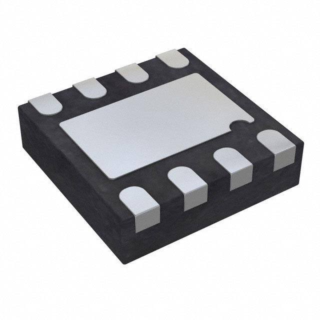
| 供应商器件封装 | 8-LFCSP-UD(2x2) |
| 其它名称 | ADP223ACPZ-R7CT |
| 包装 | 剪切带 (CT) |
| 商标 | Analog Devices |
| 安装类型 | 表面贴装 |
| 安装风格 | SMD/SMT |
| 封装 | Reel |
| 封装/外壳 | 8-UFDFN 裸露焊盘,CSP |
| 封装/箱体 | LFCSP-8 |
| 工作温度 | -40°C ~ 125°C |
| 工厂包装数量 | 3000 |
| 最大工作温度 | + 125 C |
| 最小工作温度 | - 40 C |
| 标准包装 | 1 |
| 电压-跌落(典型值) | 0.12V @ 300mA |
| 电压-输入 | 2.5 V ~ 5.5 V |
| 电压-输出 | 0.5 V ~ 5 V |
| 电流-输出 | 300mA |
| 电流-限制(最小值) | 340mA |
| 稳压器拓扑 | 正,可调式 |
| 稳压器数 | 2 |
| 系列 | ADP223 |
| 视频文件 | http://www.digikey.cn/classic/video.aspx?PlayerID=1364138032001&width=640&height=505&videoID=2245193149001 |
| 输出电流 | 300 mA |


- 商务部:美国ITC正式对集成电路等产品启动337调查
- 曝三星4nm工艺存在良率问题 高通将骁龙8 Gen1或转产台积电
- 太阳诱电将投资9.5亿元在常州建新厂生产MLCC 预计2023年完工
- 英特尔发布欧洲新工厂建设计划 深化IDM 2.0 战略
- 台积电先进制程称霸业界 有大客户加持明年业绩稳了
- 达到5530亿美元!SIA预计今年全球半导体销售额将创下新高
- 英特尔拟将自动驾驶子公司Mobileye上市 估值或超500亿美元
- 三星加码芯片和SET,合并消费电子和移动部门,撤换高东真等 CEO
- 三星电子宣布重大人事变动 还合并消费电子和移动部门
- 海关总署:前11个月进口集成电路产品价值2.52万亿元 增长14.8%


PDF Datasheet 数据手册内容提取
Dual, 300 mA Output, Low Noise, High PSRR Voltage Regulators Data Sheet ADP222/ADP223/ADP224/ADP225 FEATURES TYPICAL APPLICATION CIRCUITS Input voltage range: 2.5 V to 5.5 V VIN = 4.2V Small, 8-lead, 2 mm × 2 mm LFCSP package +C1 1µF R1 Initial accuracy: ±1% ON High PSRR: 70 dB at 10 kHz, 60 dB at 100 kHz, 40 dB at 1 MHz OFF R2 1 EN1 ADJ1 8 Low noise: 27 µV rms at VOUT = 1.2 V, 50 µV rms at VOUT = 2.8 V ON ADP223/ Excellent transient response OFF ADP225 VOUT1 = 2.0V 2 EN2 VOUT1 7 Low dropout voltage: 170 mV at 300 mA load +C2 1µF 65 µA typical ground current at no load, both LDOs enabled 3 GND VIN 6 Fixed output voltage from 0.8 V to 3.3 V (ADP222/ADP224) VOUT2 = 2.8V Adjustable output voltage range from 0.5 V to 5.0 V 4 ADJ2 VOUT2 5 (ADP223/ADP225) R3 +C1µ3F QOuveicrkc uoruretpnut ta dnids cthhaerrgmea (lQ pOroDt)e—ctAioDnP 224/ADP225 R4 09376-001 Figure 1. ADP223/ADP225 APPLICATIONS VIN = 4.2V Portable and battery-powered equipment +C1 Portable medical devices 1µF Post dc-to-dc regulation ON OFF Point of sale terminals 1 EN1 SENSE1 8 Credit card readers ON ADP222/ OFF ADP224 VOUT1 = 1.5V Automatic meter readers 2 EN2 VOUT1 7 +C2 Wireless network equipment 1µF 3 GND VIN 6 VOUT2 = 3.3V 4 SENSE2 VOUT2 5 +C3 1µF 09376-101 Figure 2. ADP222/ADP224 GENERAL DESCRIPTION The 300 mA, adjustable dual output ADP223/ADP225 and 100 kHz while operating with a low headroom voltage. The fixed dual output ADP222/ADP224 combine high PSRR, low ADP222/ADP223/ADP224/ADP225 offer much lower noise noise, low quiescent current, and low dropout voltage in a performance than competing LDOs without the need for a voltage regulator that is ideally suited for wireless applications noise bypass capacitor. Overcurrent and thermal protection with demanding performance and board space requirements. circuitry prevent damage in adverse conditions. The ADP222/ADP224 are available with fixed outputs voltages The ADP224 and ADP225 are identical to the ADP222 and from 0.8V to 3.3V. The adjustable output ADP223/ADP225 may ADP223, respectively, but with the addition of a quick output be set to output voltages from 0.5 V to 5.0 V. The low quiescent discharge (QOD) feature. current, low dropout voltage, and wide input voltage range of The ADP222/ADP223/ADP224/ADP225 are available in a the ADP222/ADP223/ADP224/ADP225 extend the battery life small 8-lead, 2 mm × 2 mm LFCSP package and are stable with of portable devices. tiny 1 µF, ±30% ceramic output capacitors, resulting in the smallest The ADP222/ADP223/ADP224/ADP225 maintain power possible board area for a wide variety of portable power needs. supply rejection greater than 60 dB for frequencies as high as Rev. E Document Feedback Information furnished by Analog Devices is believed to be accurate and reliable. However, no responsibility is assumed by Analog Devices for its use, nor for any infringements of patents or other One Technology Way, P.O. Box 9106, Norwood, MA 02062-9106, U.S.A. rights of third parties that may result from its use. Specifications subject to change without notice. No license is granted by implication or otherwise under any patent or patent rights of Analog Devices. Tel: 781.329.4700 ©2011–2014 Analog Devices, Inc. All rights reserved. Trademarks and registered trademarks are the property of their respective owners. Technical Support www.analog.com
ADP222/ADP223/ADP224/ADP225 Data Sheet TABLE OF CONTENTS Features .............................................................................................. 1 Typical Performance Characteristics ..............................................7 Applications ....................................................................................... 1 Theory of Operation ...................................................................... 17 Typical Application Circuits ............................................................ 1 Applications Information .............................................................. 18 General Description ......................................................................... 1 Capacitor Selection .................................................................... 18 Revision History ............................................................................... 2 Enable Feature ............................................................................ 19 Specifications ..................................................................................... 3 Quick Output Discharge (QOD) Function ............................ 19 Input and Output Capacitor, Recommended Specifications .. 4 Current Limit and Thermal Overload Protection ................. 20 Absolute Maximum Ratings ............................................................ 5 Thermal Considerations ............................................................ 20 Thermal Data ................................................................................ 5 Printed Circuit Board Layout Considerations ....................... 22 Thermal Resistance ...................................................................... 5 Outline Dimensions ....................................................................... 23 ESD Caution .................................................................................. 5 Ordering Guide .......................................................................... 24 Pin Configuration and Function Descriptions ............................. 6 REVISION HISTORY 5/14—Rev. D to Rev. E 7/11—Rev. 0 to Rev. A Changes to Figure 1 .......................................................................... 1 Added ADP222, ADP224, and ADP225 ......................... Universal Changes to Figure 64, V Equation and Following Text ...... 17 Changes to Features Section, Applications Section, OUT1 Deleted Paralleling Outputs to Increase Output Current Section General Description Section, and Figure 2 .................................... 1 and Figure 70 ................................................................................... 19 Changes to Table 1 ............................................................................. 3 Updated Outline Dimensions ....................................................... 23 Added Figure 4; Renumbered Sequentially ................................... 6 Changes to Table 5 ............................................................................. 6 1/13—Rev. C to Rev. D Changes to Typical Performance Characteristics Section ........... 7 Changes to Table 5 ............................................................................. 6 Changes to Theory of Operation Section and Figure 62 .......... 17 Changes to Current Limit and Thermal Overload Protection Added Figure 63 ............................................................................. 17 Section ............................................................................................... 20 Added Quick Output Discharge (QOD) Function Section 8/12—Rev. B to Rev. C Added Figure 70 ............................................................................. 20 Changes to Ordering Guide .......................................................... 23 2/11—Revision 0: Initial Version 8/11—Rev. A to Rev. B Changes to Features and General Descriptions Sections ............ 1 Added Figure 64; Renumbered Sequentially .............................. 17 Changes to Theory of Operation Section .................................... 17 Changes to Output Capacitor Section ......................................... 18 Changes to Paralleling Outputs to Increase Output Current Section ............................................................................... 19 Updated Outline Dimensions ....................................................... 23 Rev. E | Page 2 of 24
Data Sheet ADP222/ADP223/ADP224/ADP225 SPECIFICATIONS V = (V + 0.5 V) or 2.5 V (whichever is greater), EN1 = EN2 = V , I = I = 10 mA, C = C = C = 1 µF, T = 25°C, IN OUT IN OUT1 OUT2 IN OUT1 OUT2 A unless otherwise noted. Table 1. Parameter Symbol Test Conditions/Comments Min Typ Max Unit INPUT VOLTAGE RANGE V T = −40°C to +125°C 2.5 5.5 V IN J OPERATING SUPPLY CURRENT I I = 0 µA 65 µA GND OUT WITH BOTH REGULATORS ON I = 0 µA, T = −40°C to +125°C 150 µA OUT J I = 10 mA 100 µA OUT I = 10 mA, T = −40°C to +125°C 200 µA OUT J I = 300 mA 300 µA OUT I = 300 mA, T = −40°C to +125°C 450 µA OUT J SHUTDOWN CURRENT I EN1 = EN2 = GND 0.2 2 µA GND-SD OUTPUT VOLTAGE ACCURACY1 V T = −40°C to +125°C OUT J I = 10 mA −1 +1 % OUT 0 µA < I < 300 mA, V = (V + 0.5 V) to 5.5 V −2 +2 % OUT IN OUT ADJUSTABLE-OUTPUT VOLTAGE V T = −40°C to +125°C ADJ J ACCURACY1 I = 10 mA 0.495 0.500 0.505 V OUT 0 µA < I < 300 mA, V = (V + 0.5 V) to 5.5 V 0.490 0.510 V OUT IN OUT LINE REGULATION ΔV /ΔV V = (V + 0.5 V) to 5.5 V 0.01 %/V OUT IN IN OUT V = (V + 0.5 V) to 5.5 V, T = −40°C to +125°C −0.05 +0.05 %/V IN OUT J LOAD REGULATION2 ΔV /ΔI I = 1 mA to 300 mA 0.001 %/mA OUT OUT OUT I = 1 mA to 300 mA, T = −40°C to +125°C 0.002 %/mA OUT J DROPOUT VOLTAGE3 V V = 3.3 V DROPOUT OUT I = 10 mA 6 mV OUT I = 10 mA, T = −40°C to +125°C 9 mV OUT J I = 300 mA 170 mV OUT I = 300 mA, T = −40°C to +125°C A 260 mV OUT J SENSE INPUT BIAS CURRENT SENSE 2.5 V ≤ V ≤ 5.5 V, SENSEx connected to VOUTx 10 nA I-BIAS IN ADJx INPUT BIAS CURRENT ADJ 2.5 V ≤ V ≤ 5.5 V, ADJx connected to VOUTx 10 nA I-BIAS IN START-UP TIME4 t V = 3.3 V 240 µs START-UP OUT V = 0.8 V 100 µs OUT CURRENT-LIMIT THRESHOLD5 I 340 400 mA LIMIT THERMAL SHUTDOWN Thermal Shutdown Threshold TS T rising 155 °C SD J Thermal Shutdown Hysteresis TS 15 °C SD-HYS EN INPUT EN Input Logic High V 2.5 V ≤ V ≤ 5.5 V 1.2 V IH IN EN Input Logic Low V 2.5 V ≤ V ≤ 5.5 V 0.4 V IL IN EN Input Leakage Current V EN1 = EN2 = V or GND 0.1 µA I-LEAKAGE IN EN1 = EN2 = V or GND, T = −40°C to +125°C 1 µA IN J UNDERVOLTAGE LOCKOUT UVLO Input Voltage Rising UVLO 2.45 V RISE Input Voltage Falling UVLO 2.2 V FALL Hysteresis UVLOHYS 120 mV OUTPUT DISCHARGE TIME t V = 2.8 V 1000 µs DIS OUT OUTPUT DISCHARGE RESISTANCE R 140 Ω QOD Rev. E | Page 3 of 24
ADP222/ADP223/ADP224/ADP225 Data Sheet Parameter Symbol Test Conditions/Comments Min Typ Max Unit OUTPUT NOISE OUT 10 Hz to 100 kHz, V = 5 V, V = 3.3 V 56 µV rms NOISE IN OUT 10 Hz to 100 kHz, V = 5 V, V = 2.8 V 50 µV rms IN OUT 10 Hz to 100 kHz, V = 3.6 V, V = 2.5 V 45 µV rms IN OUT 10 Hz to 100 kHz, V = 3.6 V, V = 1.2 V 27 µV rms IN OUT POWER SUPPLY REJECTION RATIO PSRR V = 2.5 V, V = 0.8 V, I = 100 mA IN OUT OUT 100 Hz 76 dB 1 kHz 76 dB 10 kHz 70 dB 100 kHz 60 dB 1 MHz 40 dB V = 3.8 V, V = 2.8 V, I = 100 mA IN OUT OUT 100 Hz 68 dB 1 kHz 68 dB 10 kHz 68 dB 100 kHz 60 dB 1 MHz 40 dB 1 Accuracy when VOUTx is connected directly to ADJx or SENSEx. When the VOUTx voltage is set by external feedback resistors, the absolute accuracy in adjust mode depends on the tolerances of resistors used. 2 Based on an end-point calculation using 1 mA and 300 mA loads. 3 Dropout voltage is defined as the input-to-output voltage differential when the input voltage is set to the nominal output voltage. This applies only for output voltages above 2.5 V. 4 Start-up time is defined as the time between the rising edge of EN to VOUT being at 90% of its nominal value. 5 Current-limit threshold is defined as the current at which the output voltage drops to 90% of the specified typical value. For example, the current limit for a 3.0 V output voltage is defined as the current that causes the output voltage to drop to 90% of 3.0 V or 2.7 V. INPUT AND OUTPUT CAPACITOR, RECOMMENDED SPECIFICATIONS The minimum input and output capacitance should be greater than 0.70 µF over the full range of the operating conditions. The full range of the operating conditions in the application must be considered during device selection to ensure that the minimum capacitance specification is met. X7R and X5R type capacitors are recommended for use with the LDOs, but Y5V and Z5U capacitors are not recommended for use with the LDOs. Table 2. Parameter Symbol Conditions Min Typ Max Unit MINIMUM INPUT AND OUTPUT CAPACITANCE C T = −40°C to +125°C 0.70 µF MIN A CAPACITOR ESR R T = −40°C to +125°C 0.001 1 Ω ESR A Rev. E | Page 4 of 24
Data Sheet ADP222/ADP223/ADP224/ADP225 ABSOLUTE MAXIMUM RATINGS Junction-to-ambient thermal resistance (θ ) of the package is JA Table 3. based on modeling and calculation using a 4-layer board. θ JA Parameter Rating is highly dependent on the application and board layout. In VIN to GND −0.3 V to +6 V applications where high maximum power dissipation exists, ADJ1, ADJ2, VOUT1, VOUT2 to GND −0.3 V to VIN close attention to thermal board design is required. The value EN1, EN2 to GND −0.3 V to +6 V of θ may vary, depending on PCB material, layout, and JA Storage Temperature Range −65°C to +150°C environmental conditions. The specified value of θ is based JA Operating Junction Temperature Range −40°C to +125°C on a 4-layer, 4 in × 3 in, 2½ oz copper board, as per JEDEC Soldering Conditions JEDEC J-STD-020 standards. For more information, see the AN-772 Application Stresses above those listed under Absolute Maximum Ratings Note, A Design and Manufacturing Guide for the Lead Frame may cause permanent damage to the device. This is a stress Chip Scale Package (LFCSP). rating only; functional operation of the device at these or any Ψ is the junction-to-board thermal characterization parameter JB other conditions above those indicated in the operational with units of °C/W. Ψ of the package is based on modeling and JB section of this specification is not implied. Exposure to absolute calculation using a 4-layer board. The JESD51-12, Guidelines for maximum rating conditions for extended periods may affect Reporting and Using Package Thermal Information, states that device reliability. thermal characterization parameters are not the same as thermal THERMAL DATA resistances. ΨJB measures the component power flowing through multiple thermal paths rather than a single path as in Absolute maximum ratings apply individually only, not in thermal resistance, θ . Therefore, Ψ thermal paths include JB JB combination. convection from the top of the package as well as radiation from The ADP222/ADP223/ADP224/ADP225 can be damaged when the package, factors that make Ψ more useful in real-world JB the junction temperature limits are exceeded. Monitoring applications. Maximum junction temperature (T) is calculated J ambient temperature does not guarantee that TJ is within the from the board temperature (TB) and power dissipation (PD) specified temperature limits. In applications with high power using the formula dissipation and poor thermal resistance, the maximum ambient T = T + (P × Ψ ) J B D JB temperature may have to be derated. In applications with moderate power dissipation and low PCB thermal resistance, the Refer to JESD51-8 and JESD51-12 for more detailed maximum ambient temperature can exceed the maximum limit as information about ΨJB. long as the junction temperature is within specification limits. THERMAL RESISTANCE The junction temperature (T) of the device is dependent on the J θ and Ψ are specified for the worst-case conditions, that is, a ambient temperature (T ), the power dissipation of the device JA JB A device soldered in a circuit board for surface-mount packages. (P ), and the junction-to-ambient thermal resistance of the D package (θJA). Maximum junction temperature (TJ) is calculated Table 4. Thermal Resistance from the ambient temperature (TA) and power dissipation (PD) Package Type θJA θJC ΨJB Unit using the formula 8-Lead 2 mm × 2 mm LFCSP 50.2 31.7 18.2 °C/W T = T + (P × θ ) J A D JA ESD CAUTION Rev. E | Page 5 of 24
ADP222/ADP223/ADP224/ADP225 Data Sheet PIN CONFIGURATION AND FUNCTION DESCRIPTIONS ADP222/ ADP223/ ADP224 ADP225 1 EN1 SENSE1 8 1 EN1 ADJ1 8 2 EN2 VOUT1 7 2 EN2 VOUT1 7 3 GND VIN 6 3 GND VIN 6 4 SENSE2 VOUT2 5 4 ADJ2 VOUT2 5 N1.OCTOENSNECT EXPOSEDPADTO GND. 09376-102 N1.OCTOENSNECT EXPOSEDPADTO GND. 09376-002 Figure 3. ADP222/ADP224 Pin Configuration Figure 4. ADP223/ADP225 Pin Configuration Table 5. Pin Function Descriptions Pin No. ADP222/ADP224 ADP223/ADP225 Mnemonic Description 1 1 EN1 Enable Input for the First Regulator. Drive EN1 high to turn on Regulator 1 and drive EN1 low to turn off Regulator 1. For automatic startup, connect EN1 to VIN. 2 2 EN2 Enable Input for the Second Regulator. Drive EN2 high to turn on Regulator 2 and drive EN2 low to turn off Regulator 2. For automatic startup, connect EN2 to VIN. 3 3 GND Ground Pin. N/A1 4 ADJ2 Adjust Pin for VOUT2. A resistor divider from VOUT2 to ADJ2 sets the output voltage. 4 N/A1 SENSE2 Sense Pin for VOUT2. 5 5 VOUT2 Regulated Output Voltage. Connect an 1 μF or greater output capacitor between VOUT2 and GND. 6 6 VIN Regulator Input Supply. Bypass VIN to GND with a 1 μF or greater capacitor. 7 7 VOUT1 Regulated Output Voltage. Connect 1 μF or greater output capacitor between VOUT1 and GND. N/A1 8 ADJ1 Adjust Pin for VOUT1. A resistor divider from VOUT1 to ADJ1 sets the output voltage. 8 N/A1 SENSE1 Sense Pin for VOUT1. EPAD The exposed paddle must be connected to ground. 1 N/A means not applicable. Rev. E | Page 6 of 24
Data Sheet ADP222/ADP223/ADP224/ADP225 TYPICAL PERFORMANCE CHARACTERISTICS V = 5 V, V = 3.3 V, V = 2.8 V, I = I = 1 mA, C = C = 1 µF, T = 25°C, unless otherwise noted. IN OUT1 OUT2 OUT1 OUT2 IN OUT A 3.40 1.220 LOAD = 100µA 3.38 LOAD = 1mA 1.215 LOAD = 10mA 3.36 LOAD = 50mA LOAD = 100mA 1.210 3.34 LOAD = 300mA 1.205 3.32 V) V) (UT3.30 (UT1.200 O O V V 3.28 1.195 3.26 LOAD = 10µA 1.190 LOAD = 100µA 3.24 LOAD = 1mA LOAD = 10mA 1.185 LOAD = 100mA 3.22 LOAD = 300mA 3.20 –40 JU–N5CTION TEM25PERATURE 8(5°C) 125 09376-105 1.180 –40 JU–N5CTION TEM25PERATURE 8(5°C) 125 09376-108 Figure 5. Output Voltage vs. Junction Temperature, VOUTx = 3.3 V, Figure 8. Output Voltage vs. Junction Temperature, VOUTx = 1.2 V, ADP222/ADP224 ADP222/ADP224 2.85 3.40 2.84 LOAD = 10µA 3.38 LOAD = 100µA LOAD = 1mA 2.83 LOAD = 10mA 3.36 LOAD = 100mA 2.82 LOAD = 300mA 3.34 2.81 3.32 V) V) (UT2.80 (UT3.30 O O V V 2.79 3.28 2.78 3.26 2.77 3.24 2.76 3.22 2.75 –40 JU–N5CTION TEM25PERATURE 8(5°C) 125 09376-106 3.200.01 0.1 1ILOAD (mA)10 100 1000 09376-109 Figure 6. Output Voltage vs. Junction Temperature, VOUTx = 2.8 V, Figure 9. Output Voltage vs. Load Current, VOUTx = 3.3 V, ADP222/ADP224 ADP222/ADP224 1.820 2.85 2.84 1.815 2.83 1.810 2.82 1.805 2.81 V) V) (UT1.800 (UT2.80 O O V V 2.79 1.795 LOAD = 10µA 2.78 1.790 LOAD = 100µA LOAD = 1mA 2.77 LOAD = 10mA 1.785 LOAD = 100mA LOAD = 300mA 2.76 1.780 –40 JU–5NCTION TEM25PERATURE 8(5°C) 125 09376-107 2.750.01 0.1 1ILOAD (mA)10 100 1000 09376-110 Figure 7. Output Voltage vs. Junction Temperature, VOUTx = 1.8 V, Figure 10. Output Voltage vs. Load Current, VOUTx = 2.8 V, ADP222/ADP224 ADP222/ADP224 Rev. E | Page 7 of 24
ADP222/ADP223/ADP224/ADP225 Data Sheet 1.820 2.85 2.84 1.815 2.83 1.810 2.82 1.805 2.81 V) V) (OUT1.800 (OUT2.80 V V 1.795 2.79 2.78 LOAD = 10µA 1.790 LOAD = 100µA LOAD = 1mA 2.77 LOAD = 10mA 1.785 LOAD = 100mA 2.76 LOAD = 300mA 1.7800.01 0.1 1ILOAD (mA)10 100 1000 09376-111 2.753.7 3.9 4.1 4.3 4.V5IN (V4).7 4.9 5.1 5.3 5.5 09376-114 Figure 11. Output Voltage vs. Load Current, VOUTx = 1.8 V, ADP222/ADP224 Figure 14. Output Voltage vs. Input Voltage, VOUTx = 2.8 V, ADP222/ADP224 1.220 1.820 1.215 1.815 1.210 1.810 1.205 1.805 V (V)OUT1.200 V (V)OUT1.800 1.195 1.795 LOAD = 10µA 1.190 1.790 LOAD = 100µA LOAD = 1mA LOAD = 10mA 1.185 1.785 LOAD = 100mA LOAD = 300mA 1.1800.01 0.1 1ILOAD (mA)10 100 1000 09376-112 1.7802.30 2.70 3.10 3.50 V3IN.9 (0V) 4.30 4.70 5.10 5.50 09376-115 Figure 12. Output Voltage vs. Load Current, VOUTx = 1.2 V, ADP222/ADP224 Figure 15. Output Voltage vs. Input Voltage, VOUTx = 1.8 V, ADP222/ADP224 3.40 1.220 3.38 1.215 3.36 1.210 3.34 3.32 1.205 V (V)OUT33..2380 V (V)OUT1.200 1.195 3.26 LOAD = 10µA LOAD = 10µA LOAD = 100µA LOAD = 100µA 3.24 LLOOAADD == 110mmAA 1.190 LLOOAADD == 11m0mAA 3.22 LLOOAADD == 130000mmAA 1.185 LLOOAADD == 130000mmAA 3.203.7 3.9 4.1 4.3 4.V5IN (V4).7 4.9 5.1 5.3 5.5 09376-113 1.1802.30 2.70 3.10 3.50 V3IN.9 (0V) 4.30 4.70 5.10 5.50 09376-116 Figure 13. Output Voltage vs. Input Voltage, VOUTx = 3.3 V, ADP222/ADP224 Figure 16. Output Voltage vs. Input Voltage, VOUTx = 1.2 V, ADP222/ADP224 Rev. E | Page 8 of 24
Data Sheet ADP222/ADP223/ADP224/ADP225 140 250 120 200 A) 100 A) RENT (µ 80 RENT (µ150 R R U U C C D 60 D N N100 U U O O GR 40 LOAD = 10µA GR LOAD = 100µA LOAD = 1mA 50 20 LOAD = 10mA LOAD = 100mA LOAD = 300mA 0 –40 JU–N5CTION TEM25PERATURE8 (5°C) 125 09376-117 00.01 0.1 1ILOAD (mA)10 100 1000 09376-120 Figure 17. Ground Current vs. Junction Temperature, Single Output, Figure 20. Ground Current vs. Load Current, Dual Output, ADP222/ADP224 ADP222/ADP224 300 140 LOAD = 100µA LOAD = 50mA LOAD = 1mA LOAD = 100mA 250 LOAD = 10mA LOAD = 300mA 120 A) A)100 T (µ 200 T (µ N N RE RE 80 R R U 150 U C C D D 60 N N U U O 100 O GR GR 40 50 20 LLOOAADD == 1100µ0µAA LLOOAADD == 1100m0mAA LOAD = 1mA LOAD = 300mA 0 0 –40 JU–N5CTION TEM2P5ERATURE 8(5°C) 125 09376-118 2.30 2.70 3.10 3.50 V3IN.9 (0V) 4.30 4.70 5.10 5.50 09376-121 Figure 18. Ground Current vs. Junction Temperature, Dual Output, Figure 21. Ground Current vs. Input Voltage, VOUTx = 1.2 V, ADP222/ADP224 ADP222/ADP224 140 250 120 200 A)100 A) T (µ T (µ REN 80 REN150 R R U U C C D 60 D N N100 U U O O GR 40 GR 50 20 LOAD = 10µA LOAD = 10mA LOAD = 100µA LOAD = 100mA LOAD = 1mA LOAD = 300mA 0 0 0.01 0.1 1ILOAD (mA)10 100 1000 09376-119 2.30 2.70 3.10 3.50 V3IN.9 (0V) 4.30 4.70 5.10 5.50 09376-122 Figure 19. Ground Current vs. Load Current, Single Output, ADP222/ADP224 Figure 22. Ground Current vs. Input Voltage, VOUTx = 1.2 V and 1.8 V, ADP222/ADP224 Rev. E | Page 9 of 24
ADP222/ADP223/ADP224/ADP225 Data Sheet 3.40 1.220 3.38 1.215 3.36 1.210 3.34 1.205 3.32 V) V) (UT3.30 (UT1.200 O O V V 3.28 1.195 3.26 LOAD = 100µA 1.190 LOAD = 100µA 3.24 LOAD = 1mA LOAD = 1mA LOAD = 10mA LOAD = 10mA LOAD = 50mA 1.185 LOAD = 50mA 3.22 LOAD = 100mA LOAD = 100mA LOAD = 300mA LOAD = 300mA 3.20 1.180 –40 JU–N5CTION TEM2P5ERATURE8 (5°C) 125 09376-003 –40 JU–N5CTION TEM2P5ERATURE8 (5°C) 125 09376-006 Figure 23. Output Voltage vs. Junction Temperature, VOUTx = 3.3 V, Figure 26. Output Voltage vs. Junction Temperature, VOUTx = 1.2 V, ADP223/ADP225 ADP223/ADP225 2.85 3.40 2.84 3.38 2.83 3.36 2.82 3.34 V (V)OUT22..8801 V (V)OUT33..3302 2.79 3.28 2.78 3.26 LOAD = 100µA 2.77 LOAD = 1mA 3.24 LOAD = 10mA LOAD = 50mA 2.76 LOAD = 100mA 3.22 LOAD = 300mA 2.75 3.20 –40 JU–N5CTION TEM2P5ERATURE8 (5°C) 125 09376-004 0.1 1 ILOAD10 (mA) 100 1000 09376-007 Figure 24. Output Voltage vs. Junction Temperature, VOUTx = 2.8 V, Figure 27. Output Voltage vs. Load Current, VOUTx = 3.3 V, ADP223/ADP225 ADP223/ADP225 1.820 2.85 1.815 2.84 2.83 1.810 2.82 1.805 2.81 V) V) (UT1.800 (UT2.80 O O V V 2.79 1.795 2.78 1.790 LOAD = 100µA LOAD = 1mA 2.77 LOAD = 10mA 1.785 LOAD = 50mA LOAD = 100mA 2.76 LOAD = 300mA 1.780 2.75 –40 JU–N5CTION TEM25PERATURE8 (5°C) 125 09376-005 0.01 0.1 1ILOAD (mA)10 100 1000 09376-008 Figure 25. Output Voltage vs. Junction Temperature, VOUTx = 1.8 V, Figure 28. Output Voltage vs. Load Current, VOUTx = 2.8 V, ADP223/ADP225 ADP223/ADP225 Rev. E | Page 10 of 24
Data Sheet ADP222/ADP223/ADP224/ADP225 1.820 2.85 2.84 1.815 2.83 1.810 2.82 1.805 2.81 V) V) (UT1.800 (UT 2.80 O O V V 2.79 1.795 2.78 1.790 LOAD = 100µA 2.77 LOAD = 1mA LOAD = 10mA 1.785 2.76 LOAD = 50mA LOAD = 200mA LOAD = 300mA 1.780 2.75 0.1 1 ILOAD10 (mA) 100 1000 09376-009 3.50 3.70 3.90 4.10 4.3V0IN (V4).70 4.90 5.10 5.30 5.50 09376-012 Figure 29. Output Voltage vs. Load Current, VOUTx = 1.8 V, ADP223/ADP225 Figure 32. Output Voltage vs. Input Voltage, VOUTx = 2.8 V, ADP223/ADP225 1.220 1.820 1.215 1.815 1.210 1.810 1.205 1.805 V) V) (UT1.200 (UT1.800 O O V V 1.195 1.795 1.190 1.790 LOAD = 100µA LOAD = 1mA LOAD = 10mA 1.185 1.785 LOAD = 50mA LOAD = 100mA LOAD = 300mA 1.180 1.780 0.1 1 ILOAD10 (mA) 100 1000 09376-010 2.30 2.70 3.10 3.50 V3IN.9 (0V) 4.30 4.70 5.10 5.50 09376-013 Figure 30. Output Voltage vs. Load Current, VOUTx = 1.2 V, ADP223/ADP225 Figure 33. Output Voltage vs. Input Voltage, VOUTx = 1.8 V, ADP223/ADP225 3.40 1.220 3.38 1.215 3.36 1.210 3.34 1.205 3.32 V) V) (UT 3.30 (UT1.200 O O V V 3.28 1.195 3.26 LOAD = 100µA 1.190 LOAD = 100µA 3.24 LOAD = 1mA LOAD = 1mA LOAD = 10mA LOAD = 10mA 3.22 LOAD = 50mA 1.185 LOAD = 50mA LOAD = 100mA LOAD = 100mA LOAD = 300mA LOAD = 300mA 3.20 1.180 3.70 3.90 4.10 4.30 V4IN.7 (0V) 4.90 5.10 5.30 5.50 09376-011 2.30 2.70 3.10 3.50 V3IN.9 (0V) 4.30 4.70 5.10 5.50 09376-014 Figure 31. Output Voltage vs. Input Voltage, VOUTx = 3.3 V, ADP223/ADP225 Figure 34. Output Voltage vs. Input Voltage, VOUTx = 1.2 V, ADP223/ADP225 Rev. E | Page 11 of 24
ADP222/ADP223/ADP224/ADP225 Data Sheet 300 500 450 250 400 A) A) u µ 350 T ( 200 T ( EN EN 300 R R R R U 150 U 250 C C D D N N 200 U U O 100 O R R 150 G G LOAD = 100µA LOAD = 1mA 100 50 LOAD = 10mA LOAD = 50mA 50 LOAD = 100mA LOAD = 300mA 0 0 –40 JU–N5CTION TEM2P5ERATURE8 (5°C) 125 09376-015 0.01 0.1 1ILOAD (mA)10 100 1000 09376-018 Figure 35. Ground Current vs. Junction Temperature, Single Output, Figure 38. Ground Current vs. Load Current, Dual Output, Includes 200 µA for Includes 100 µA for Output Divider, ADP223/ADP225 Output Dividers, ADP223/ADP225 500 250 450 400 200 CURRENT (µA) 233505000 CURRENT (µA) 150 OUND 200 OUND 100 GR 150 LOAD = 100µA GR LOAD = 100µA 100 LLOOAADD == 11m0mAA 50 LLOOAADD == 11m0mAA 50 LLOOAADD == 5100m0mAA LLOOAADD == 5100m0mAA LOAD = 300mA LOAD = 300mA 0 –40 JU–N5CTION TEM2P5ERATURE8 (5°C) 125 09376-016 02.3 2.7 3.1 3.5 VI3N. 9(V) 4.3 4.7 5.1 5.5 09376-019 Figure 36. Ground Current vs. Junction Temperature, Dual Output, Includes Figure 39. Ground Current vs. Input Voltage, VOUTx = 1.2 V, Single Output, 200 µA for Output Dividers, ADP223/ADP225 Includes 100 µA for Output Divider, ADP223/ADP225 250 450 400 200 350 GROUND CURRENT (µA) 110500 GROUND CURRENT (µA) 122350500000 LOAD = 100µA 50 100 LOAD = 1mA LOAD = 10mA 50 LOAD = 50mA LOAD = 200mA LOAD = 300mA 00.01 0.1 1ILOAD (mA)10 100 1000 09376-017 02.3 2.7 3.1 3.5 VI3N. 9(V) 4.3 4.7 5.1 5.5 09376-020 Figure 37. Ground Current vs. Load Current, Single Output, Figure 40. Ground Current vs. Input Voltage, VOUTx = 1.2 V and 1.8 V, Includes 100 µA for Output Divider, ADP223/ADP225 Dual Output, Includes 200 µA for Output Dividers, ADP223/ADP225 Rev. E | Page 12 of 24
Data Sheet ADP222/ADP223/ADP224/ADP225 140 2.90 2.85 120 2.80 V) m 100 2.75 E ( UT VOLTAG 6800 V (V)OUT222...667050 O P RO 40 2.55 D LOAD = 1mA 2.50 LOAD = 5mA LOAD = 10mA 20 LOAD = 50mA 2.45 LOAD = 100mA LOAD = 300mA 01 10 ILOAD (mA) 100 1000 09376-021 2.402.6 2.7 2.8 VIN (V) 2.9 3.0 3.1 09376-024 Figure 41. Dropout Voltage vs. Load Current, VOUT = 3.3 V Figure 44. Output Voltage vs. Input Voltage in Dropout, VOUTx = 2.8 V 160 450 400 140 350 V) 120 A) m µ E ( T ( 300 G 100 N TA RE 250 L R O 80 U V C T D 200 U N O 60 U OP RO 150 R G D 40 LOAD = 100µA 100 LOAD = 1mA LOAD = 10mA 20 50 LOAD = 50mA LOAD = 100mA LOAD = 300mA 01 10 ILOAD (mA) 100 1000 09376-022 03.1 3.2 3.3 VIN (V) 3.4 3.5 3.6 09376-025 Figure 42. Dropout Voltage vs. Load Current, VOUT = 2.8 V Figure 45. Ground Current vs. Input Voltage in Dropout, VOUTx = 3.3 V 3.40 400 3.35 350 3.30 A) 300 3.25 u NT ( 250 V)3.20 RE V (OUT3.15 D CUR 200 3.10 UN 150 O 3.05 GR LOAD = 1mA 100 LOAD = 100µA 3.00 LOAD = 5mA LOAD = 1mA LOAD = 10mA LOAD = 10mA 2.95 LLOOAADD == 5100m0mAA 50 LLOOAADD == 5100m0mAA LOAD = 300mA LOAD = 300mA 2.90 0 3.1 3.2 3.3 VIN (V) 3.4 3.5 3.6 09376-023 2.6 2.7 2.8 VIN (V) 2.9 3.0 3.1 09376-026 Figure 43. Output Voltage vs. Input Voltage in Dropout, VOUTx = 3.3 V Figure 46. Ground Current vs. Input Voltage in Dropout, VOUTx = 2.8 V Rev. E | Page 13 of 24
ADP222/ADP223/ADP224/ADP225 Data Sheet 0 0 VRIPPLE = 50mV LOAD = 100µA VRIPPLE = 50mV LOAD = 1mA ––2100 VVCIOONUU =TT 4==. 331V.µ3FV LLLLOOOOAAAADDDD ==== 1113m000m00AmmAAA ––2100 VCVIOONUU =TT 2==. 511V.µ2FV LLLOOOAAADDD === 113000m00mmAAA –30 –30 B) –40 B) –40 R (d –50 R (d –50 R R S S P –60 P –60 –70 –70 –80 –80 –90 –90 –10010 100 1kFREQU1E0NkCY (Hz)100k 1M 10M 09376-027 –10010 100 1kFREQU1E0NkCY (Hz)100k 1M 10M 09376-030 Figure 47. Power Supply Rejection Ratio vs. Frequency, Figure 50. Power Supply Rejection Ratio vs. Frequency, VIN = 4.3, V VOUTx = 3.3 V VIN = 2.5 V, VOUTx = 1.2 V 0 0 ––2100 VVVCRIOONIUUP =TTP L3==E. 821 =V.µ8 F5V0mV LLLLLOOOOOAAAAADDDDD ===== 111130m0000m00AmmµAAAA ––2100 VCVVIORONIUUP =TTP L3==E. 831 =V.µ3 F5V0mV LLLLOOOOAAAADDDD ==== 1113m000m00AmmAAA –30 –30 PSRR (dB) –––654000 PSRR (dB) –––654000 –70 –70 –80 –80 –90 –90 –10010 100 1kFREQU1E0NkCY (Hz)100k 1M 10M 09376-028 –10010 100 1kFREQU1E0NkCY (Hz)100k 1M 10M 09376-031 Figure 48. Power Supply Rejection Ratio vs. Frequency, Figure 51. Power Supply Rejection Ratio vs. Frequency, VIN = 3.8 V, VOUTx = 2.8 V VIN = 3.8 V, VOUTx = 3.3 V 0 0 ––2100 VCVVRIOONIUUP =TTP L2==E. 811 =V.µ8 F5V0mV LLLLOOOOAAAADDDD ==== 1113m000m00AmmAAA ––2100 VVCVRIOONIUUP =TTP L3==E. 321 =V.µ8 F5V0mV LLLLOOOOAAAADDDD ==== 1113m000m00AmmAAA –30 –30 B) –40 B) –40 R (d –50 R (d –50 R R PS –60 PS –60 –70 –70 –80 –80 –90 –90 –10010 100 1kFREQU1E0NkCY (Hz)100k 1M 10M 09376-029 –10010 100 1kFREQU1E0NkCY (Hz)100k 1M 10M 09376-032 Figure 49. Power Supply Rejection Ratio vs. Frequency, Figure 52. Power Supply Rejection Ratio vs. Frequency, VIN = 2.8 V, VOUTx = 1.8 V VIN = 3.3 V, VOUTx = 2.8 V Rev. E | Page 14 of 24
Data Sheet ADP222/ADP223/ADP224/ADP225 0 VRIPPLE = 50mV –10 VIN = 2.5V VOUT = 1.8V –20 COUT = 1µF VIN –30 B) –40 R (d –50 2 VOUT1 R S P –60 –70 VOUT2 3 –80 LOAD = 1mA 1 –90 LOAD = 10mA LOAD = 100mA LOAD = 300mA –10010 100 1kFREQU1E0NkCY (Hz)100k 1M 10M 09376-033 CCHH13 11V0mV BBWW CH2 10mV BW MT 1 9µ.s8%A CH4 200mV 09376-036 Figure 53. Power Supply Rejection Ratio vs. Frequency, Figure 56. Transient Line Response, VOUTx = 3.3 V and 2.8 V, VIN = 4 V to 5 V, VIN = 2.5 V, VOUTx = 1.8 V ILOAD = 300 mA VIN VIN 2 VOUT1 2 VOUT1 VOUT2 VOUT2 3 3 1 1 CCHH13 11V0mV BBWW CH2 10mV BW MT 1 1µ0s.40A% CH4 200mV 09376-034 CCHH13 11V0mV BBWW CH2 10mV BW MT 1 1µ0s.00A% CH4 200mV 09376-037 Figure 54. Transient Line Response, VOUTx = 3.3 V and 2.8 V, VIN = 4 V to 5 V, Figure 57. Transient Line Response, VOUTx = 1.2 V and 1.8 V, VIN = 4 V to 5 V, ILOAD = 10 mA ILOAD = 300 mA LOAD CURRENT ON VOUT1 VIN 1 2 VOUT1 2 VOUT1 VOUT2 3 VOUT2 1 3 CCHH13 11V0mV BBWW CH2 10mV BW MT 4 9µ.s8%A CH4 200mV 09376-035 CCHH13 21000mmVA ΩBBWW CH2 50mV BW MT 1 010µ.s20A% CH1 200mA 09376-038 Figure 55. Transient Line Response, VOUTx = 1.2 V and 1.8 V, VIN = 4 V to 5 V, Figure 58. Transient Load Response, VOUTx = 3.3 V, ILOAD = 1 mA to 300 mA; ILOAD = 10 mA VOUTx = 2.8 V, ILOAD = 1 mA Rev. E | Page 15 of 24
ADP222/ADP223/ADP224/ADP225 Data Sheet 10 1.2V LOAD CURRENT 1.8V ON VOUT1 Hz) 32..38VV √ 1 µV/ TY ( 1 SI N E D 2 L VOUT1 RA T C PE 0.1 VOUT2 E S 3 OIS N CCHH13 21000.0mmAVΩBBWW CH2 50mV BW MT 1 010µ.s20A% CH1 200mA 09376-039 0.0110 100 FREQUE1NkCY (Hz) 10k 100k 09376-041 Figure 59. Transient Load Response, VOUTx = 1.2 V, ILOAD = 1 mA to 300 mA; Figure 61. Output Noise Spectral Density, VIN = 5 V, ILOAD = 10 mA, COUT = 1 μF VOUTx = 1.8 V, ILOAD = 1 mA 70 60 50 s) m V r 40 µ E ( OIS 30 N 20 1.2V 10 1.8V 2.8V 3.3V 00.001 0.01 0.1 ILOAD1 (mA) 10 100 1000 09376-040 Figure 60. RMS Output Noise vs. Load Current and Output Voltage, VIN = 5 V, COUT = 1 µF Rev. E | Page 16 of 24
Data Sheet ADP222/ADP223/ADP224/ADP225 THEORY OF OPERATION The ADP222/ADP223/ADP224/ADP225 are low quiescent controlled by the error amplifier. The error amplifier compares current, fixed and adjustable dual output, low dropout linear the reference voltage with the feedback voltage from the output regulators that operate from 2.5 V to 5.5 V and provide up to and amplifies the difference. If the feedback voltage is lower 300 mA of current from each output. Drawing a low 300 μA than the reference voltage, the gate of the PMOS device is quiescent current (typical) at full load make the ADP222/ pulled lower, allowing more current to flow and increasing the ADP223/ADP224/ADP225 ideal for battery-operated portable output voltage. If the feedback voltage is higher than the equipment. Shutdown current consumption is typically 200 nA. reference voltage, the gate of the PMOS device is pulled higher, allowing less current to flow and decreasing the output voltage. Optimized for use with small 1 μF ceramic capacitors, the ADP222/ADP223/ADP224/ADP225 provide excellent VIN= 4.2V transient performance. +C1 1µF R1 ADJ1 ON OFF R2 ADP223/ADP225 1 EN1 ADJ1 8 VIN VOUT1 ON ADP223/ OFF ADP225 VOUT1 = 2.0V 2 EN2 VOUT1 7 140Ω +C2 THERMAL CURRENT 1µF SHUTDOWN LIMIT 3 GND VIN 6 VOUT2 = 2.8V 4 ADJ2 VOUT2 5 EN1 CONTROL R3 +C1µ3F EN2 ELNAOANGBDILCE REFERENCE ADP225 ONLY R4 09376-064 Figure 64. Typical Application Circuit for Setting Output Voltages, ADP223/ADP225 CURRENT The ADP223/ADP225 are exactly the same as the ADP222/ LIMIT 140Ω ADP224 except that the output voltage dividers are internally GND disconnected and the feedback input of the error amplifiers is VOUT2 brought out for each output. The output voltages can be set ADJ2 09376-062 according to the following equations: Figure 62. Internal Block Diagram, ADP223/ADP225 V = 0.50 V(1 + R2/R1) OUT1 SENSE1 V = 0.50 V(1 + R3/R4) OUT2 ADP222/ADP224 The value of R1 and R4 should be less than 200 kΩ to minimize VIN VOUT1 errors in the output voltage caused by the ADJx pin input current. For example, when R1 and R2 each equal 200 kΩ, the output 140Ω THERMAL CURRENT voltage is 1.0 V. The output voltage error introduced by the ADJx SHUTDOWN LIMIT pin input current is 2 mV or 0.20%, assuming a typical ADJx pin input current of 10 nA at 25°C. EN1 CONTROL The output voltage of the ADP223/ADP225 may be set from LOGIC ADP224 AND REFERENCE ONLY 0.5 V to 5.0 V. EN2 ENABLE The ADP222/ADP224 are available in multiple output voltage options ranging from 0.8 V to 3.3 V. CURRENT The ADP224/ADP225 are identical to the ADP222/ADP223 LIMIT 140Ω with the addition of a quick output discharge (QOD) feature. GND This allows the output voltage to start up from a known state. VOUT2 SENSE2 09376-063 tToh een AabDleP 2a2n2d/ AdiDsaPb2le2 3th/Ae DVPO2U2T4/1A/VDOP2U2T52 u psien tsh uen EdNer1 n/EorNm2a pl ins Figure 63. Internal Block Diagram, ADP222/ADP224 operating conditions. When EN1/EN2 are high, VOUT1/VOUT2 turn on; when EN1/EN2 are low, VOUT1/VOUT2 turn off. For Internally, the ADP222/ADP223/ADP224/ADP225 consist of a automatic startup, EN1/EN2 can be tied to VIN. reference, two error amplifiers, and two PMOS pass transistors. Output current is delivered via the PMOS pass device, which is Rev. E | Page 17 of 24
ADP222/ADP223/ADP224/ADP225 Data Sheet APPLICATIONS INFORMATION CAPACITOR SELECTION Figure 66 depicts the capacitance vs. voltage bias characteristic Output Capacitor of an 0402, 1 µF, 10 V, X5R capacitor. The voltage stability of a capacitor is strongly influenced by the capacitor size and voltage The ADP222/ADP223/ADP224/ADP225 are designed for rating. In general, a capacitor in a larger package or higher voltage operation with small, space-saving ceramic capacitors but rating exhibits better stability. The temperature variation of the function with most commonly used capacitors as long as care is X5R dielectric is ~±15% over the −40°C to +85°C temperature taken with regard to the effective series resistance (ESR) value. range and is not a function of package or voltage rating. The ESR of the output capacitor affects the stability of the LDO 1.2 control loop. A minimum of 0.7 µF capacitance with an ESR of 1 Ω or less is recommended to ensure the stability of the ADP222/ 1.0 ADP223/ADP224/ADP225. Transient response to changes in load current is also affected by output capacitance. Using a F) 0.8 larger value of output capacitance improves the transient response E (µ of the ADP222/ADP223/ADP224/ADP225 to large changes in NC A 0.6 load current. Figure 65 shows the transient responses for an CIT A output capacitance value of 1 µF. P CA 0.4 LOAD CURRENT 0.2 ON VOUT1 1 00 2 4VOLTAGE (V6) 8 10 09376-044 Figure 66. Capacitance vs. Voltage Bias Characteristic 2 VOUT1 Use Equation 1 to determine the worst-case capacitance accounting for capacitor variation over temperature, component tolerance, and voltage. VOUT2 C = C × (1 − TEMPCO) × (1 − TOL) (1) 3 EFF BIAS where: CCHH13 21000mmVAΩBBWW CH2 50mV BW MT 1 010µ.s20%A CH1 200mA 09376-043 CTEBIMAS PisC thOe i es ftfhecet wivoer csat-pcaacsieta cnacpea caitt tohre t eompepreartaintugr ve oclotaegffei.c ient. Figure 65. Output Transient Response, COUT = 1 µF TOL is the worst-case component tolerance. Input Bypass Capacitor In this example, the worst-case temperature coefficient (TEMPCO) Connecting a 1 µF capacitor from VIN to GND reduces the over −40°C to +85°C is assumed to be 15% for an X5R dielectric. circuit sensitivity to the printed circuit board (PCB) layout, The tolerance of the capacitor (TOL) is assumed to be 10%, and especially when long input traces or high source impedance C is 0.94 µF at 1.8 V, as shown in Figure 66. BIAS are encountered. If greater than 1 µF of output capacitance is Substituting these values in Equation 1 yields required, the input capacitor should be increased to match it. C = 0.94 µF × (1 − 0.15) × (1 − 0.1) = 0.719 µF Input and Output Capacitor Properties EFF Therefore, the capacitor chosen in this example meets the Any good quality ceramic capacitors can be used with the minimum capacitance requirement of the LDO over temperature ADP222/ADP223/ADP224/ADP225, as long as they meet the and tolerance at the chosen output voltage. minimum capacitance and maximum ESR requirements. Ceramic capacitors are manufactured with a variety of To guarantee the performance of the ADP222/ADP223/ dielectrics, each with different behavior over temperature and ADP224/ADP225, it is imperative that the effects of dc bias, applied voltage. Capacitors must have a dielectric adequate to temperature, and tolerances on the behavior of the capacitors ensure the minimum capacitance over the necessary temperature be evaluated for each application. range and dc bias conditions. X5R or X7R dielectrics with a voltage rating of 6.3 V or 10 V are recommended, but Y5V and Z5U dielectrics are not recommended, due to their poor temperature and dc bias characteristics. Rev. E | Page 18 of 24
Data Sheet ADP222/ADP223/ADP224/ADP225 ENABLE FEATURE 3.5 ENx 3.3V The ADP222/ADP223/ADP224/ADP225 use the ENx pins to 3.0 21..88VV enable and disable the VOUTx pins under normal operating 1.2V conditions. Figure 67 shows a rising voltage on ENx crossing V) 2.5 E ( the active threshold, where V turns on. When a falling G OUTx TA 2.0 voltage on ENx crosses the inactive threshold, VOUTx turns off. OL V 1.4 VIN = 5.5V PUT 1.5 T U 1.2 O 1.0 V) 1.0 0.5 E ( G UT VOLTA 00..68 00 100 200 300 400TIM5E0 0(µs)600 700 800 900 1000 09376-047 TP Figure 69. Typical Start-Up Time U O 0.4 QUICK OUTPUT DISCHARGE (QOD) FUNCTION 0.2 The ADP224/ADP225 include an output discharge resistor to force the voltage on each output to zero when the respective 0 0.5 0.6 0.7 ENA0B.8LE VO0L.T9AGE (1V.)0 1.1 1.2 09376-045 LalDwOay si si nd ias awbellel-dd. eTfihniesd e sntsauter,e rse tghaart dthlees so uift pitu itss eonf athbele LdD oOr ns oarte. Figure 67. Typical ENx Pin Operation, VIN = 5.5 V The ADP222/ADP223 do not include the output discharge As shown in Figure 67, the ENx pins have built-in hysteresis. function. Figure 70 compares the turn-off time of a 3.3 V output This prevents on/off oscillations that can occur due to noise on LDO with and without the QOD function. Both LDOs have a the ENx pins as it passes through the threshold points. 1 kΩ resistor connected to each output. The LDO with the QOD function discharges the output to 0 V in less than 1 ms, The active/inactive thresholds of the ENx pins are derived from whereas the 1 kΩ load takes over 5 ms to do the same. the VIN voltage. Therefore, these thresholds vary with changing 4.0 input voltage. Figure 68 shows typical ENx active/inactive thresholds when the input voltage varies from 2.5 V to 5.5 V. 3.5 1.2 ENABLE ENx FALL 3.0 VOUT, NO QOD ENx RISE VOUT, WITH QOD 1.0 2.5 V) DS (V) 0.8 OLTS ( 2.0 L V HO 1.5 S RE 0.6 H 1.0 T E L B 0.4 0.5 A N E 0.2 00 2000 4000TIME (µs6)000 8000 10000 09376-169 02.3 2.7 3.1 3.5 VI3N. 9(V) 4.3 4.7 5.1 5.5 09376-046 Figure 70. Typical Turn-Off Time with and Without QOD Function Figure 68. Typical Enable Thresholds vs. Input Voltage The ADP222/ADP223/ADP224/ADP225 use an internal soft start to limit the inrush current when the output is enabled. The start-up time for the 2.8 V option is approximately 240 µs from the time the ENx active threshold is crossed to when the output reaches 90% of its final value. The start-up time is somewhat dependent on the output voltage setting and increases slightly as the output voltage increases. Rev. E | Page 19 of 24
ADP222/ADP223/ADP224/ADP225 Data Sheet CURRENT LIMIT AND THERMAL OVERLOAD THERMAL CONSIDERATIONS PROTECTION In most applications, the ADP222/ADP223/ADP224/ADP225 The ADP222/ADP223/ADP224/ADP225 are protected against do not dissipate much heat due to its high efficiency. However, damage due to excessive power dissipation by current and in applications with high ambient temperature, and high supply thermal overload protection circuits. The ADP222/ADP223/ voltage to output voltage differential, the heat dissipated in ADP224/ADP225 are designed to current limit when the output the package is large enough that it can cause the junction load reaches 300 mA (typical). When the output load exceeds temperature of the die to exceed the maximum junction 300 mA, the output voltage is reduced to maintain a constant temperature of 125°C. current limit. When the junction temperature exceeds 155°C, the converter Thermal overload protection is included, which limits the enters thermal shutdown. It recovers only after the junction junction temperature to a maximum of 155°C (typical). Under temperature has decreased below 140°C to prevent any permanent extreme conditions (that is, high ambient temperature and damage. Therefore, thermal analysis for the chosen application power dissipation) when the junction temperature starts to rise is very important to guarantee reliable performance over all above 155°C, the output is turned off, reducing the output current conditions. The junction temperature of the die is the sum of to 0. When the junction temperature drops below 140°C, the the ambient temperature of the environment and the temperature output is turned on again, and output current is restored to its rise of the package due to the power dissipation, as shown in nominal value. Equation 2. Consider the case where a hard short from VOUTx to ground To guarantee reliable operation, the junction temperature of occurs. At first, the ADP222/ADP223/ADP224/ADP225 cur- the ADP222/ADP223/ADP224/ADP225 must not exceed rent limits, so that only 300 mA is conducted into the short. If 125°C. To ensure that the junction temperature stays below this self-heating of the junction is great enough to cause its tempera- maximum value, the user must be aware of the parameters that ture to rise above 155°C, thermal shutdown activates, turning contribute to junction temperature changes. These parameters off the output and reducing the output current to 0 mA. As the include ambient temperature, power dissipation in the power junction temperature cools and drops below 140°C, the output device, and thermal resistances between the junction and ambient turns on and conducts 300 mA into the short, again causing the air (θJA). The θJA number is dependent on the package assembly junction temperature to rise above 155°C. This thermal oscilla- compounds that are used and the amount of copper used to tion between 140°C and 155°C causes a current oscillation solder the package GND pin to the PCB. between 300 mA and 0 mA that continues as long as the short Table 6 shows typical θ values of the 8-lead LFCSP package for JA remains at the output. various PCB copper sizes, and Table 7 shows the typical Ψ value JB Current and thermal limit protections are intended to protect of the 8-lead LFCSP. the device against accidental overload conditions. For reliable operation, device power dissipation must be externally limited Table 6. Typical θ Values JA so that junction temperatures do not exceed 125°C. Copper Size (mm2) θ (°C/W) JA 251 175.1 100 135.6 500 77.3 1000 65.2 6400 51 1 Device soldered to minimum size pin traces. Table 7. Typical Ψ Value JB Model ΨJB (°C/W) 8-Lead LFCSP 18.2 Rev. E | Page 20 of 24
Data Sheet ADP222/ADP223/ADP224/ADP225 140 The junction temperature of the ADP222/ADP223/ADP224/ ADP225 can be calculated by 120 C) TJ = TA + (PD × θJA) (2) E T (°J100 R where: U T A 80 TA is the ambient temperature. ER P PD is the power dissipation in the die, given by EM 60 T P = [(V − V ) × I ] + (V × I ) N 6400mm2 D IN OUT LOAD IN GND TIO 40 1000mm2 where: UNC 510000mmmm22 ILOAD is the load current. J 20 25mm2 JEDEC IGND is the ground current. TJ MAX PVoINw aenrd d VissOiUpTa atrioe nin dpuuet taon gdr oouutnpdu tc uvorrletangte iss, qreusiptee csmtivaellly a. nd can 00 0.2 TOTA0L.4 POWER0 D.6ISSIPATI0O.8N (W) 1.0 1.2 09376-049 be ignored. Therefore, the junction temperature equation Figure 72. 8-Lead LFCSP, TA = 50°C simplifies to the following: 140 T = T + {[(V − V ) × I ] × θ } J A IN OUT LOAD JA 120 C) Atesm spheorwatnu rien, itnhpeu sti-m top-loifuietpdu et qvuoalttaigoen d, fifofre rae ngtiivael,n a anmd bcioenntti nuous E T (°J100 R U load current, there exists a minimum copper size requirement T A 80 R for the PCB to ensure that the junction temperature does not rise E P M above 125°C. Figure 71 to Figure 74 show junction temperature E 60 T calculations for different ambient temperatures, power dissipation, N 6400mm2 and areas of PCB copper. CTIO 40 1500000mmmm22 UN 100mm2 140 J 20 25mm2 JEDEC 120 TJ MAX E T (°C)J100 00 0.2 TOTA0L.4 POWER0 D.6ISSIPATI0O.8N (W) 1.0 1.2 09376-050 R TU Figure 73. 8-Lead LFCSP, TA = 85°C A 80 ER 140 P M E 60 N T 6400mm2 C) 120 UNCTIO 40 1510000000mmmmmm222 RE T (°J100 J 20 25mm2 TU JEDEC A 80 R TJ MAX PE 00 0.2 TOTA0L.4 POWER0 D.6ISSIPATI0O.8N (W) 1.0 1.2 09376-048 ON TEM 60 Figure 71. 8-Lead LFCSP, TA = 25°C CTI 40 N JU TB = 25°C 20 TB = 50°C TB = 85°C TJ MAX 00 1 TO2TAL POW3ER DISS4IPATION 5(W) 6 7 09376-051 Figure 74. 8-Lead LFCSP, TA = 85°C In the case where the board temperature is known, use the thermal characterization parameter, Ψ , to estimate the JB junction temperature rise (see Figure 74). Maximum junction temperature (T) is calculated from the board temperature (T ) J B and power dissipation (P ) using the following formula: D T = T + (P × Ψ ) (3) J B D JB The typical value of Ψ is 18.2°C/W for the 8-lead LFCSP package. JB Rev. E | Page 21 of 24
ADP222/ADP223/ADP224/ADP225 Data Sheet PRINTED CIRCUIT BOARD LAYOUT TB1 CONSIDERATIONS GND 1 T Heat dissipation from the package can be improved by U TB5 increasing the amount of copper attached to the pins of the J1 O V ADP222/ADP223/ADP224/ADP225. However, as listed in TB2 R1 R2 Table 6, a point of diminishing returns is eventually reached 1 N beyond which an increase in the copper size does not yield E significant heat dissipation benefits. U1 C2 N Place the input capacitor as close as possible to the VIN and TB3 C1 TB4 VI GND pins. Place the output capacitor as close as possible to the 2 J2 N C3 VOUTx and GND pins. Use of 0402 or 0603 size capacitors and E R4 resistors achieves the smallest possible footprint solution on R3 boards where area is limited. 2 T ADP223 - ________- EVALZ TB6 U O ANALOG TB7 V DEVICES GND 09376-052 Figure 75. Example 8-Lead LFCSP PCB Layout Rev. E | Page 22 of 24
Data Sheet ADP222/ADP223/ADP224/ADP225 OUTLINE DIMENSIONS 1.70 1.60 2.10 1.50 2.00 SQ 1.90 0.50 BSC 5 8 0.15 REF PIN 1 INDEX EXPOSED 1.10 AREA PAD 1.00 0.425 0.90 0.350 0.275 4 1 PIN 1 TOP VIEW BOTTOM VIEW INDICATOR (R 0.15) 0.60 FOR PROPER CONNECTION OF 0.55 0.05 MAX THE EXPOSED PAD, REFER TO THE PIN CONFIGURATION AND 0.50 0.02 NOM FUNCTION DESCRIPTIONS SECTION OF THIS DATA SHEET. SEPALTAINNGE 000...322050 0.20 REF 01-14-2013-C Figure 76. 8-Lead Lead Frame Chip Scale Package [LFCSP_UD] 2.00 mm × 2.00 mm Body, Ultra Thin, Dual Lead (CP-8-10) Dimensions shown in millimeters Rev. E | Page 23 of 24
ADP222/ADP223/ADP224/ADP225 Data Sheet ORDERING GUIDE Output Voltage (V) Model1 Temperature Range VOUT1 VOUT2 Package Description Package Option Branding ADP222ACPZ-1218-R7 −40°C to +125°C 1.2 1.8 8-Lead Lead Frame Chip Scale CP-8-10 L16 Package [LFCSP_UD] ADP222ACPZ-1228-R7 −40°C to +125°C 1.2 2.8 8-Lead Lead Frame Chip Scale CP-8-10 L17 Package [LFCSP_UD] ADP222ACPZ-1233-R7 −40°C to +125°C 1.2 3.3 8-Lead Lead Frame Chip Scale CP-8-10 L18 Package [LFCSP_UD] ADP222ACPZ-1528-R7 −40°C to +125°C 1.5 2.8 8-Lead Lead Frame Chip Scale CP-8-10 LKR Package [LFCSP_UD] ADP222ACPZ-1533-R7 −40°C to +125°C 1.5 3.3 8-Lead Lead Frame Chip Scale CP-8-10 LKS Package [LFCSP_UD] ADP222ACPZ-1815-R7 −40°C to +125°C 1.8 1.5 8-Lead Lead Frame Chip Scale CP-8-10 LL0 Package [LFCSP_UD] ADP222ACPZ-1825-R7 −40°C to +125°C 1.8 2.5 8-Lead Lead Frame Chip Scale CP-8-10 LL1 Package [LFCSP_UD] ADP222ACPZ-1827-R7 −40°C to +125°C 1.8 2.7 8-Lead Lead Frame Chip Scale CP-8-10 L3A Package [LFCSP_UD] ADP222ACPZ-1833-R7 −40°C to +125°C 1.8 3.3 8-Lead Lead Frame Chip Scale CP-8-10 LL2 Package [LFCSP_UD] ADP222ACPZ-2725-R7 −40°C to +125°C 2.7 2.5 8-Lead Lead Frame Chip Scale CP-8-10 LN8 Package [LFCSP_UD] ADP222ACPZ-2818-R7 −40°C to +125°C 2.8 1.8 8-Lead Lead Frame Chip Scale CP-8-10 LL3 Package [LFCSP_UD] ADP222ACPZ-2827-R7 −40°C to +125°C 2.8 2.7 8-Lead Lead Frame Chip Scale CP-8-10 LJE Package [LFCSP_UD] ADP222ACPZ-3325-R7 −40°C to +125°C 3.3 2.5 8-Lead Lead Frame Chip Scale CP-8-10 LKV Package [LFCSP_UD] ADP222ACPZ-3328-R7 −40°C to +125°C 3.3 2.8 8-Lead Lead Frame Chip Scale CP-8-10 LKW Package [LFCSP_UD] ADP222ACPZ-3330-R7 −40°C to +125°C 3.3 3.0 8-Lead Lead Frame Chip Scale CP-8-10 LKX Package [LFCSP_UD] ADP224ACPZ-2818-R7 −40°C to +125°C 2.8 1.8 8-Lead Lead Frame Chip Scale CP-8-10 LKP Package [LFCSP_UD] ADP225ACPZ-R7 −40°C to +125°C Adjustable Adjustable 8-Lead Lead Frame Chip Scale CP-8-10 LKQ Package [LFCSP_UD] ADP223ACPZ-R7 −40°C to +125°C Adjustable Adjustable 8-Lead Lead Frame Chip Scale CP-8-10 LJQ Package [LFCSP_UD] ADP223CP-EVALZ Adjustable Adjustable Evaluation Board ADP225CP-EVALZ Adjustable Adjustable Evaluation Board 1 Z = RoHS Compliant Part. ©2011–2014 Analog Devices, Inc. All rights reserved. Trademarks and registered trademarks are the property of their respective owners. D09376-0-5/14(E) Rev. E | Page 24 of 24
Mouser Electronics Authorized Distributor Click to View Pricing, Inventory, Delivery & Lifecycle Information: A nalog Devices Inc.: ADP223ACPZ-R7 ADP222ACPZ-3325-R7 ADP222ACPZ-1233-R7 ADP225ACPZ-R7 ADP222ACPZ-1833-R7 ADP222ACPZ-1815-R7 ADP222ACPZ-1825-R7 ADP223CP-EVALZ ADP222ACPZ-1218-R7 ADP222ACPZ-3328-R7 ADP222ACPZ-3330-R7 ADP222ACPZ-1533-R7 ADP225CP-EVALZ ADP222ACPZ-1528-R7 ADP222ACPZ-1827- R7 ADP222ACPZ-2827-R7 ADP222ACPZ-2725-R7 ADP224ACPZ-2818-R7 ADP222ACPZ-2818-R7 ADP222ACPZ- 1228-R7