ICGOO在线商城 > 集成电路(IC) > PMIC - 稳压器 - DC DC 开关稳压器 > ADP2164ACPZ-R7

 Datasheet下载
- 型号: ADP2164ACPZ-R7
- 制造商: Analog
- 库位|库存: xxxx|xxxx
- 要求:
| 数量阶梯 | 香港交货 | 国内含税 |
| +xxxx | $xxxx | ¥xxxx |
查看当月历史价格
查看今年历史价格
ADP2164ACPZ-R7产品简介:
ICGOO电子元器件商城为您提供ADP2164ACPZ-R7由Analog设计生产,在icgoo商城现货销售,并且可以通过原厂、代理商等渠道进行代购。 ADP2164ACPZ-R7价格参考。AnalogADP2164ACPZ-R7封装/规格:PMIC - 稳压器 - DC DC 开关稳压器, Buck Switching Regulator IC Positive Adjustable 0.6V 1 Output 4A 16-WQFN Exposed Pad, CSP。您可以下载ADP2164ACPZ-R7参考资料、Datasheet数据手册功能说明书,资料中有ADP2164ACPZ-R7 详细功能的应用电路图电压和使用方法及教程。
ADP2164ACPZ-R7是Analog Devices Inc.推出的一款同步降压型DC-DC开关稳压器,广泛应用于对电源效率和空间布局要求较高的电子设备中。其典型应用场景包括便携式设备(如智能手机、平板电脑)、电池供电系统、工业便携仪器以及嵌入式系统等。该器件支持宽输入电压范围(2.7V至5.5V),可提供两路独立的可调或固定输出电压,适用于为处理器、FPGA、ASIC、传感器及低功耗微控制器等核心芯片供电。

ADP2164ACPZ-R7采用电流模式控制架构,具备快速瞬态响应能力,能有效应对负载变化,确保输出电压稳定。其高达3MHz的开关频率允许使用小型电感和陶瓷电容,有助于减小整体电源方案的尺寸,适合高密度PCB设计。此外,器件集成多种保护功能,如过流保护、过温保护和软启动机制,提升了系统可靠性。

在工业自动化、通信模块(如Wi-Fi、蓝牙模块)和医疗便携设备中,ADP2164ACPZ-R7也常用于构建高效、低噪声的电源轨。其封装形式为16引脚LFCSP(3mm × 3mm),便于表面贴装,适用于自动化生产流程。总体而言,ADP2164ACPZ-R7是一款高性能、小尺寸、高集成度的双通道降压稳压器,适用于需要高效能电源管理的多种现代电子应用场合。
| 参数 | 数值 |
| 产品目录 | 集成电路 (IC)半导体 |
| 描述 | IC REG BUCK SYNC ADJ 4A 16LFCSP稳压器—开关式稳压器 6.5V 4A Hi Eff Step-Down |
| 产品分类 | |
| 品牌 | Analog Devices Inc |
| 产品手册 | |
| 产品图片 | |
| rohs | 符合RoHS无铅 / 符合限制有害物质指令(RoHS)规范要求 |
| 产品系列 | 电源管理 IC,稳压器—开关式稳压器,Analog Devices ADP2164ACPZ-R7- |
| 数据手册 | |
| 产品型号 | ADP2164ACPZ-R7 |
| PCN组件/产地 | |
| PWM类型 | 电流模式 |
| 产品种类 | 稳压器—开关式稳压器 |
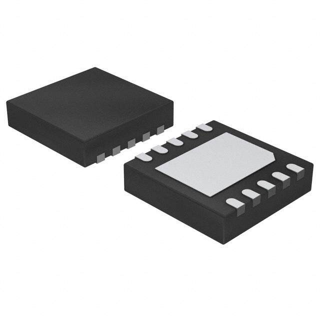
| 供应商器件封装 | 16-LFCSP-WQ(4x4) |
| 其它名称 | ADP2164ACPZ-R7DKR |
| 包装 | Digi-Reel® |
| 参考设计库 | http://www.digikey.com/rdl/4294959904/4294959903/1139 |
| 同步整流器 | 是 |
| 商标 | Analog Devices |
| 安装类型 | 表面贴装 |
| 安装风格 | SMD/SMT |
| 宽度 | 4 mm |
| 封装 | Reel |
| 封装/外壳 | 16-WQFN 裸露焊盘,CSP |
| 封装/箱体 | LFCSP-16 |
| 工作温度 | -40°C ~ 125°C |
| 工厂包装数量 | 1500 |
| 开关频率 | 600 kHz |
| 最大工作温度 | + 125 C |
| 最大输入电压 | 6.5 V |
| 最小工作温度 | - 40 C |
| 最小输入电压 | 2.7 V |
| 标准包装 | 1 |
| 电压-输入 | 2.7 V ~ 6.5 V |
| 电压-输出 | 0.6 V ~ 6.5 V |
| 电流-输出 | 4A |
| 类型 | 降压(降压) |
| 系列 | ADP2164 |
| 视频文件 | http://www.digikey.cn/classic/video.aspx?PlayerID=1364138032001&width=640&height=505&videoID=2245193149001 |
| 负载调节 | 0.05 %/A |
| 输出数 | 1 |
| 输出电压 | Adj |
| 输出电流 | 4 A |
| 输出端数量 | 1 |
| 输出类型 | 可调式 |
| 频率-开关 | 500kHz ~ 1.4MHz |


- 商务部:美国ITC正式对集成电路等产品启动337调查
- 曝三星4nm工艺存在良率问题 高通将骁龙8 Gen1或转产台积电
- 太阳诱电将投资9.5亿元在常州建新厂生产MLCC 预计2023年完工
- 英特尔发布欧洲新工厂建设计划 深化IDM 2.0 战略
- 台积电先进制程称霸业界 有大客户加持明年业绩稳了
- 达到5530亿美元!SIA预计今年全球半导体销售额将创下新高
- 英特尔拟将自动驾驶子公司Mobileye上市 估值或超500亿美元
- 三星加码芯片和SET,合并消费电子和移动部门,撤换高东真等 CEO
- 三星电子宣布重大人事变动 还合并消费电子和移动部门
- 海关总署:前11个月进口集成电路产品价值2.52万亿元 增长14.8%


PDF Datasheet 数据手册内容提取
6.5 V, 4 A, High Efficiency, Step-Down, DC-to-DC Regulator Data Sheet ADP2164 FEATURES TYPICAL APPLICATIONS CIRCUIT 4 A continuous output current R1 VIN 43 mΩ and 29 mΩ integrated FET C1 CIN R2 ±1.5% output accuracy Input voltage range: 2.7 V to 6.5 V PGOODVIN PVIN L Output voltage: 0.6 V to VIN EN SW VOUT Switching frequency COUT SYNC FB ADP2164 Fixed frequency: 600 kHz or 1.2 MHz TRK PGND Adjustable frequency: 500 kHz to 1.4 MHz Synchronizable from 500 kHz to 1.4 MHz RT GND SCeulrercetnatb mleo sdyen achrcrhointeizcet uprhea se shift: 0° or 180° RT 09944-001 Figure 1. Precision enable input Power-good output Voltage tracking input 100 Integrated soft start 95 Internal compensation 90 Starts up into a precharged output 85 UVLO, OVP, OCP, and thermal shutdown %) Available in 16-lead, 4 mm × 4 mm LFCSP package Y ( 80 C Supported by ADIsimPower™ design tool EN 75 CI FI 70 APPLICATIONS F E 65 Point-of-load conversion 60 Communications and networking equipment Industrial and instrumentation 55 VfSI N= =6 050VkHz VVOOUUTT == 13..23VV Consumer electronics 500 0.5 1.0 OU1T.5PUT C2U.0RREN2T. 5(A) 3.0 3.5 4.009944-002 Figure 2. Efficiency vs. Output Current GENERAL DESCRIPTION The ADP2164 is a 4 A, synchronous, step-down, dc-to-dc regulator The ADP2164 integrates a pair of low on-resistance P-channel in a compact 4 mm × 4 mm LFCSP package. The regulator uses a and N-channel internal MOSFETs to maximize efficiency and current mode, constant frequency pulse-width modulation (PWM) minimize external component count. The 100% duty cycle control scheme for excellent stability and transient response. operation allows low dropout voltage at 4 A output current. The input voltage range of the ADP2164 is 2.7 V to 6.5 V. The The high, 1.2 MHz PWM switching frequency allows the use of output voltage of the ADP2164 is adjustable from 0.6 V to the small external components, and the SYNC input enables multiple input voltage (V ). The ADP2164 is also available in six preset ICs to synchronize out of phase to reduce ripple and eliminate IN output voltage options: 3.3 V, 2.5 V, 1.8 V, 1.5 V, 1.2 V, and 1.0 V. beat frequencies. Other key features of the ADP2164 include undervoltage lockout (UVLO), integrated soft start to limit inrush current at startup, overvoltage protection (OVP), overcurrent protection (OCP), and thermal shutdown. Rev. C Document Feedback Information furnished by Analog Devices is believed to be accurate and reliable. However, no responsibility is assumed by Analog Devices for its use, nor for any infringements of patents or other One Technology Way, P.O. Box 9106, Norwood, MA 02062-9106, U.S.A. rights of third parties that may result from its use. Specifications subject to change without notice. No license is granted by implication or otherwise under any patent or patent rights of Analog Devices. Tel: 781.329.4700 ©2011–2018 Analog Devices, Inc. All rights reserved. Trademarks and registered trademarks are the property of their respective owners. Technical Support www.analog.com
ADP2164 Data Sheet TABLE OF CONTENTS Features .............................................................................................. 1 Oscillator and Synchronization ................................................ 14 Applications ....................................................................................... 1 Power Good ................................................................................ 15 Typical Applications Circuit ............................................................ 1 Current Limit and Short-Circuit Protection ............................ 15 General Description ......................................................................... 1 Overvoltage Protection (OVP) ................................................. 15 Revision History ............................................................................... 2 Undervoltage Lockout (UVLO) ............................................... 15 Specifications ..................................................................................... 3 Thermal Shutdown .................................................................... 15 Absolute Maximum Ratings ............................................................ 5 Applications Information .............................................................. 16 Thermal Resistance ...................................................................... 5 ADIsimPower Design Tool ....................................................... 16 ESD Caution .................................................................................. 5 Output Voltage Selection ........................................................... 16 Pin Configuration and Function Descriptions ............................. 6 Inductor Selection ...................................................................... 16 Typical Performance Characteristics ............................................. 7 Output Capacitor Selection....................................................... 16 Functional Block Diagram ............................................................ 13 Input Capacitor Selection .......................................................... 17 Theory of Operation ...................................................................... 14 Voltage Tracking ......................................................................... 17 Control Scheme .......................................................................... 14 Applications Circuits ...................................................................... 18 Slope Compensation .................................................................. 14 Outline Dimensions ....................................................................... 19 Precision Enable/Shutdown ...................................................... 14 Ordering Guide .......................................................................... 19 Integrated Soft Start ................................................................... 14 REVISION HISTORY 6/2018—Rev. B to Rev. C 6/2012—Rev. 0 to Rev. A Updated Outline Dimensions ....................................................... 19 Changes to Features Section ............................................................ 1 Changes to Ordering Guide .......................................................... 19 Added ADIsimPower Design Tool Section ................................. 16 8/2017—Rev. A to Rev. B 12/2011—Revision 0: Initial Version Changed CP-16-26 to CP-16-17 .................................. Throughout Updated Outline Dimensions ....................................................... 19 Changes to Ordering Guide .......................................................... 19 Rev. C | Page 2 of 19
Data Sheet ADP2164 SPECIFICATIONS VIN = PVIN = 3.3 V, EN high, SYNC high, T = −40°C to +125°C, unless otherwise noted. Typical values are at T = 25°C. J J Table 1. Parameter Symbol Test Conditions/Comments Min Typ Max Unit VIN AND PVIN PINS VIN Voltage Range VIN 2.7 6.5 V PVIN Voltage Range PVIN 2.7 6.5 V Quiescent Current I No switching 895 1100 µA VIN Shutdown Current I VIN = PVIN = 6.5 V, EN = GND 9 12 µA SHDN VIN Undervoltage Lockout Threshold UVLO VIN rising 2.6 2.7 V VIN falling 2.4 2.5 V OUTPUT CHARACTERISTICS Specified by the circuit in Figure 42 Load Regulation I = 0 A to 4 A 0.05 %/A O Line Regulation I = 2 A 0.05 %/V O FB PIN FB Regulation Voltage V T = −40°C to +125°C 0.591 0.6 0.609 V FB J FB Bias Current I 0.01 0.1 µA FB SW PIN High-Side On Resistance1 VIN = PVIN = 3.3 V, I = 500 mA 35 52 70 mΩ SW VIN = PVIN = 5 V, I = 500 mA 30 43 55 mΩ SW Low-Side On Resistance1 VIN = PVIN = 3.3 V, I = 500 mA 24 32 40 mΩ SW VIN = PVIN = 5 V, I = 500 mA 20 29 35 mΩ SW SW Peak Current Limit High-side switch, PVIN = 3.3 V 5 6.2 7.4 A SW Maximum Duty Cycle Full frequency 100 % SW Minimum On Time2 Full frequency 100 ns TRK PIN TRK Input Voltage Range 0 600 mV TRK to FB Offset Voltage TRK = 0 mV to 500 mV −15 +15 mV TRK Input Bias Current 100 nA FREQUENCY Switching Frequency f RT = VIN 1.08 1.2 1.32 MHz S RT = GND 540 600 660 kHz RT = 91 kΩ 480 600 720 kHz Switching Frequency Range 500 1400 kHz RT Pin Input High Voltage 1.2 V RT Pin Input Low Voltage 0.45 V SYNC PIN Synchronization Range 0.5 1.4 MHz Minimum Pulse Width 100 ns Minimum Off Time 100 ns Input High Voltage 1.2 V Input Low Voltage 0.4 V PGOOD PIN Power-Good Range FB rising threshold 105 110 115 % FB rising hysteresis 2.5 % FB falling threshold 85 90 95 % FB falling hysteresis 2.5 % Power-Good Deglitch Time From FB to PGOOD 16 Clock cycles Power-Good Leakage Current V = 5 V 0.1 1 µA PGOOD Power-Good Output Low Voltage I = 1 mA 170 220 mV PGOOD Rev. C | Page 3 of 19
ADP2164 Data Sheet Parameter Symbol Test Conditions/Comments Min Typ Max Unit INTEGRATED SOFT START Soft Start Time All switching frequencies 2048 Clock cycles EN PIN EN Input Rising Threshold 1.12 1.2 1.28 V EN Input Hysteresis 100 mV EN Pull-Down Resistor 1 MΩ THERMAL SHUTDOWN Thermal Shutdown Threshold T increasing 140 °C J Thermal Shutdown Hysteresis 15 °C 1 Pin-to-pin measurements. 2 Guaranteed by design. Rev. C | Page 4 of 19
Data Sheet ADP2164 ABSOLUTE MAXIMUM RATINGS THERMAL RESISTANCE Table 2. Parameter Rating θ is measured using natural convection on a JEDEC 4-layer JA PVIN, VIN, SW −0.3 V to +7 V board. The exposed pad is soldered to the printed circuit board FB, SYNC, TRK, RT, EN, PGOOD −0.3 V to +7 V with thermal vias. PGND to GND −0.3 V to +0.3 V Table 3. Thermal Resistance Operating Junction Temperature Range −40°C to +125°C Package Type θ Unit Storage Temperature Range −65°C to +150°C JA Soldering Conditions JEDEC J-STD-020 16-Lead LFCSP 38.3 °C/W Stresses at or above those listed under Absolute Maximum ESD CAUTION Ratings may cause permanent damage to the product. This is a stress rating only; functional operation of the product at these or any other conditions above those indicated in the operational section of this specification is not implied. Operation beyond the maximum operating conditions for extended periods may affect product reliability. Rev. C | Page 5 of 19
ADP2164 Data Sheet PIN CONFIGURATION AND FUNCTION DESCRIPTIONS D O O N GP NE NIV IVP 6 5 4 3 1 1 1 1 SYNC 1 12 PVIN RT 2 ADP2164 11 SW TOP VIEW TRK 3 (Not to Scale) 10 SW FB 4 9 SW 5 6 7 8 D D D D N N N N G G G G P P P NOTES 1 . TTTOHHEEA ENICX E FPXOOTRSE ERTDNHAEPARLD MG ASRLHO ODUIUNSLDSD IPP BALETA INSOEON L.UDNEDREERD09944-003 Figure 3. Pin Configuration Table 4. Pin Function Descriptions Pin No. Mnemonic Description 1 SYNC Synchronization Input. To synchronize the switching frequency to an external clock, connect this pin to an external clock with a frequency of 500 kHz to 1.4 MHz (see the Oscillator and Synchronization section for more information). 2 RT Frequency Setting. To select a switching frequency of 600 kHz, connect this pin to GND; to select a switching frequency of 1.2 MHz, connect this pin to VIN. To program the frequency from 500 kHz to 1.4 MHz, connect a resistor from this pin to GND (see the Oscillator and Synchronization section for more information). 3 TRK Tracking Input. To track a master voltage, connect the TRK pin to a voltage divider from the master voltage. If the tracking function is not used, connect the TRK pin to VIN. For more information, see the Voltage Tracking section. 4 FB Feedback Voltage Sense Input. Connect this pin to a resistor divider from V . For the preset output version, OUT connect this pin directly to V . OUT 5 GND Analog Ground. Connect to the ground plane. 6, 7, 8 PGND Power Ground. Connect to the ground plane and to the output return side of the output capacitor. 9, 10, 11 SW Switch Node Output. Connect to the output inductor. 12, 13 PVIN Power Input Pin. Connect this pin to the input power source. Connect a bypass capacitor between this pin and PGND. 14 VIN Bias Voltage Input Pin. Connect a bypass capacitor between this pin and GND; connect a small (10 Ω) resistor between this pin and PVIN. 15 EN Precision Enable Pin. The external resistor divider can be used to set the turn-on threshold. To enable the part automatically, connect the EN pin to VIN. This pin has a 1 MΩ pull-down resistor to GND. 16 PGOOD Power-Good Output (Open Drain). Connect this pin to a resistor from any pull-up voltage lower than 6.5 V. 17 (EPAD) Exposed Pad The exposed pad should be soldered to an external ground plane under the IC for thermal dissipation. Rev. C | Page 6 of 19
Data Sheet ADP2164 TYPICAL PERFORMANCE CHARACTERISTICS T = 25°C, V = 5 V, V = 1.2 V, L = 1 µH, C = 47 µF, C = 100 µF, unless otherwise noted. J IN OUT IN OUT 100 100 90 90 80 80 %) %) Y ( 70 Y( 70 C C N N E E FICI 60 FICI 60 F F E E 50 50 VOUT=0.6V 40 INDMUCSSTO10R3:8 C-1O52ILNCLRBAFT VVVVVOOOOOUUUUUTTTTT ===== 01112.....60285VVVVV 40 INDMUSCST1O0R38:-C1O52ILNCLRBAFT VVVVVOOOOOUUUUUTTTTT=====11123.....02853VVVVV 300 1 OUTPUT CU2RRENT (A) 3 4 09944-004 300 1 OUTPUTCU2RRENT(A) 3 4 09944-007 Figure 4. Efficiency vs. Output Current, VIN = 3.3 V, fS = 600 kHz Figure 7. Efficiency vs. Output Current, VIN = 5 V, fS = 600 kHz 100 100 90 90 80 80 %) %) Y ( 70 Y ( 70 C C N N E E FICI 60 FICI 60 F F E E 50 50 VOUT = 0.6V VOUT = 1.0V VOUT = 1.0V VOUT = 1.2V 40 VOUT = 1.2V 40 VOUT = 1.8V INDUCTOR: COILCRAFT VOUT = 1.8V INDUCTOR: COILCRAFT VOUT = 2.5V MSS1038-102NLB VOUT = 2.5V MSS1038-102NLB VOUT = 3.3V 300 1 OUTPUT CU2RRENT (A) 3 4 09944-005 300 1 OUTPUT CU2RRENT (A) 3 4 09944-008 Figure 5. Efficiency vs. Output Current, VIN = 3.3 V, fS = 1.2 MHz Figure 8. Efficiency vs. Output Current, VIN = 5 V, fS = 1.2 MHz 1050 11 10 1000 A) A) µ µ 9 T (950 T ( N N E E RR RR 8 U U C900 C T N N W 7 UIESCE850 HUTDO 6 Q S 800 TJ = –40°C TJ = –40°C TJ = +25°C 5 TJ = +25°C TJ = +125°C TJ = +125°C 7502.7 3.1 3.5 3.9 4.3VIN 4(V.7) 5.1 5.5 5.9 6.3 09944-006 42.7 3.1 3.5 3.9 4.3VIN 4(V.7) 5.1 5.5 5.9 6.3 09944-009 Figure 6. Quiescent Current vs. VIN (No Switching) Figure 9. Shutdown Current vs. VIN Rev. C | Page 7 of 19
ADP2164 Data Sheet 606 1.30 605 1.28 1.26 604 1.24 mV)603 V)1.22 RISING DBACK VOLTAGE (666550009921098 ABLE THRESHOLD (111111......211111086420 FALLING FEE597 EN1.08 1.06 596 1.04 595 1.02 594–40 –20 0 2T0EMPE4R0ATURE60 (°C) 80 100 120 09944-010 1.00–40 –20 0 2T0EMPE4R0ATURE60 (°C) 80 100 120 09944-013 Figure 10. Feedback Voltage vs. Temperature, VIN = 3.3 V Figure 13. EN Threshold vs. Temperature 80 60 70 50 Ω) Ω) m60 m R ( R (40 O O T T SIS50 SIS E E T R T R30 FE40 FE P N 20 30 TJ = –40°C TJ = –40°C TJ = +25°C TJ = +25°C TJ = +125°C TJ = +125°C 202.7 3.1 3.5 3.9 4.3VIN 4(V.7) 5.1 5.5 5.9 6.3 09944-011 102.7 3.1 3.5 3.9 4.3VIN 4(V.7) 5.1 5.5 5.9 6.3 09944-014 Figure 11. PFET Resistor vs. VIN (Pin-to-Pin Measurements) Figure 14. NFET Resistor vs. VIN (Pin-to-Pin Measurements) 1300 650 1275 640 630 1250 FREQUENCY (kHz)111221207505 FREQUENCY (kHz)666521090000 580 1150 1125 TTTJJJ === –++421052°°5CC°C 557600 TTTJJJ === –++421052°°5CC°C 11002.7 3.1 3.5 3.9 4.3VIN 4(V.7) 5.1 5.5 5.9 6.3 09944-012 5502.7 3.1 3.5 3.9 4.3VIN 4(V.7) 5.1 5.5 5.9 6.3 09944-015 Figure 12. Switching Frequency vs. VIN, fS = 1.2 MHz (RT = VIN) Figure 15. Switching Frequency vs. VIN, fS = 600 kHz (RT = GND) Rev. C | Page 8 of 19
Data Sheet ADP2164 650 2.70 2.68 640 2.66 630 2.64 2.62 RISING 620 V) Hz) D (2.60 Y (k610 HOL2.58 C S2.56 N600 E UE HR2.54 FREQ559800 UVLO T22..5502 FALLING 2.48 570 2.46 TJ = –40°C 2.44 560 TJ = +25°C TJ = +125°C 2.42 5502.7 3.1 3.5 3.9 4.3VIN 4(V.7) 5.1 5.5 5.9 6.3 09944-016 2.40–40 –20 0 2T0EMPE4R0ATURE60 (°C) 80 100 120 09944-019 Figure 16. Switching Frequency vs. VIN, fS = 600 kHz (RT = 91 kΩ) Figure 19. UVLO Threshold vs. Temperature, VIN = 3.3 V 6.8 7.0 6.6 6.8 A)6.4 A)6.6 T ( T ( LIMI6.2 LIMI6.4 T T N N E6.0 E6.2 R R R R U U K C5.8 K C6.0 A A E E P5.6 P5.8 5.4 5.6 5.2–40 –20 0 2T0EMPE4R0ATURE60 (°C) 80 100 120 09944-017 5.42.7 3.1 3.5 3.9 4.3VIN 4(V.7) 5.1 5.5 5.9 6.3 09944-020 Figure 17. Peak Current Limit vs. Temperature, VIN = 3.3 V Figure 20. Peak Current Limit vs. VIN, TJ = 25°C T T EN EN 3 3 VOUT VOUT 1 1 PGOOD PGOOD 2 2 IL IL 4 4 CCHH13 550.000mVV CCHH24 25..0000AV Ω MT 12.00.02m0%s ACH3 2.50V09944-018 CCHH13 550.000mVV CCHH24 25..0000AV Ω MT 12.00.02m0%s ACH3 2.50V09944-021 Figure 18. Soft Start with Full Load, VIN = 5 V, VOUT = 1.2 V, fS = 1.2 MHz Figure 21. Soft Start with Precharged Output Voltage, VIN = 5 V, fS = 1.2 MHz Rev. C | Page 9 of 19
ADP2164 Data Sheet T T VOUT(AC) VOUT(AC) 1 1 IO IO 4 4 CH1 100mV BWCH4 2.00A Ω MT 22000.µ20s% ACH4 2.52A09944-022 CH1 100mV BWCH4 2.00A Ω MT 22000.µ20s% ACH4 2.52A09944-025 Figure 22. Load Transient, 0.5 A to 3.5 A Load Step, Figure 25. Load Transient, 0.5 A to 3.5 A Load Step, VIN = 5 V, VOUT = 1.2 V, fS = 1.2 MHz VIN = 5 V, VOUT = 1.2 V, fS = 600 kHz T T SYNC SYNC 1 1 SW SW 2 2 CH1 5.00V CH2 2.00V MT 46000.n40s% ACH1 2.50V09944-023 CH1 5.00V CH2 2.00V MT 46000.n40s% ACH1 2.50V09944-026 Figure 23. ADP2164 Synchronized to 1 MHz, in Phase Figure 26. ADP2164 Synchronized to 1 MHz, 180° out of Phase T T VOUT VOUT 1 1 SW SW 2 2 IL IL 4 4 CH1 500mV BWCCHH24 55..0000AV ΩBWMT 23.00.02m0%s ACH1 680mV09944-024 CH1 500mV BWCCHH42 55..0000 VAΩBWMT 26.00.06m0%s ACH1 680mV09944-027 Figure 24. Output Short Figure 27. Output Short Recovery Rev. C | Page 10 of 19
Data Sheet ADP2164 T T VOUT 1 TRK IL FB 4 SW 4 2 CCHH24 550000mmVV BBWWMT 24.00.04m0%s ACH2 820mV09944-028 CH1 5.00mV CCHH24 52..0000VA Ω MT 43000.6n0s% ACH2 3.30V09944-031 Figure 28. Tracking Function Figure 31. Steady Waveform, VIN = 5 V, VOUT = 1.2 V, fS = 1.2 MHz 60 200 60 200 48 160 48 160 MAGNITUDE MAGNITUDE 36 120 36 120 24 80 24 80 MAGNITUDE (dB)–11220 PHASE 40–040 PHASE (Degrees) MAGNITUDE (dB)–11220 PHASE 40–040 PHASE (Degrees) –24 –80 –24 –80 –36 –120 –36 –120 –48 CROSS FREQUENCY: 57kHz –160 –48 CROSS FREQUENCY: 61kHz –160 PHASE MARGIN: 67° PHASE MARGIN: 69° –60 –200 –60 –200 1k 10k FREQUE1NC1Y0 0(Hkz) 12M 09944-029 1k 10k FREQUEN1C1Y0 0(Hkz) 12M 09944-032 Figure 29. Bode Plot at VIN = 5 V, VOUT = 1.0 V, IO = 4 A, fS = 1.2 MHz, Figure 32. Bode Plot at VIN = 5 V, VOUT = 1.2 V, IO = 4 A, fS = 1.2 MHz, L = 0.68 μH, COUT = 2 × 100 μF L = 0.68 μH, COUT = 47 μF + 100 μF 60 200 60 200 48 160 48 160 MAGNITUDE MAGNITUDE 36 120 36 120 24 80 24 80 MAGNITUDE (dB)–11220 PHASE 40–040 PHASE (Degrees) MAGNITUDE (dB)–11220 PHASE 40–040 PHASE (Degrees) –24 –80 –24 –80 –36 –120 –36 –120 –48 CROSS FREQUENCY: 52kHz –160 –48 CROSS FREQUENCY: 61kHz –160 PHASE MARGIN: 69° PHASE MARGIN: 66° –60 –200 –60 –200 1k 10k FREQUEN1C1Y0 0(Hkz) 12M 09944-030 1k 10k FREQUEN1C1Y0 0(Hkz) 1M2 09944-033 Figure 30. Bode Plot at VIN = 5 V, VOUT = 1.5 V, IO = 4 A, fS = 1.2 MHz, Figure 33. Bode Plot at VIN = 5 V, VOUT = 1.8 V, IO = 4 A, fS = 1.2 MHz, L = 1 μH, COUT = 47 μF + 100 μF L = 1 μH, COUT = 100 μF Rev. C | Page 11 of 19
ADP2164 Data Sheet 60 200 60 200 48 160 48 160 MAGNITUDE MAGNITUDE 36 120 36 120 24 80 24 80 UDE (dB) 120 PHASE 400 Degrees) UDE (dB) 120 PHASE 400 Degrees) MAGNIT–12 –40 PHASE ( MAGNIT–12 –40 PHASE ( –24 –80 –24 –80 –36 –120 –36 –120 –48 CROSS FREQUENCY: 83kHz –160 –48 CROSS FREQUENCY: 68kHz –160 PHASE MARGIN: 60° PHASE MARGIN: 65° –60 –200 –60 –200 1k 10k FREQUENC11Y0 0(Hkz) 1M2 09944-034 1k 10k FREQUENC11Y0 0(Hkz) 1M2 09944-035 Figure 34. Bode Plot at VIN = 5 V, VOUT = 2.5 V, IO = 4 A, fS = 1.2 MHz, Figure 35. Bode Plot at VIN = 5 V, VOUT = 3.3 V, IO = 4 A, fS = 1.2 MHz, L = 1 μH, COUT = 47 μF L = 1 μH, COUT = 47 μF Rev. C | Page 12 of 19
Data Sheet ADP2164 FUNCTIONAL BLOCK DIAGRAM VIN EN PVIN UVLO ADP2164 REGULATOR PMOS ERRORAMP 0.6V + ZCOMP SECNUSRERAEMNTP PFET TRK + LOGIC SOFT GM CONTROL SW START + FB – NFET 0.66V – + CLK – SLOPE NMOS COMPENSATION CURRENT SENSEAMP 0.54V + OSCILLATOR PGOOD GND SYNC RT PGND 09944-036 Figure 36. Functional Block Diagram Rev. C | Page 13 of 19
ADP2164 Data Sheet THEORY OF OPERATION The ADP2164 is a step-down dc-to-dc regulator that uses INTEGRATED SOFT START a fixed-frequency, peak current mode architecture with an The ADP2164 has integrated soft start circuitry to limit the integrated high-side switch and low-side synchronous rectifier. output voltage rise time and reduce inrush current at startup. The high switching frequency and tiny, 16-lead, 4 mm × 4 mm The soft start time is set at 2048 clock cycles. LFCSP package provide a small, step-down dc-to-dc regulator If the output voltage is precharged before the part is turned on, solution. The integrated high-side switch (P-channel MOSFET) the ADP2164 prevents a reverse inductor current (which would and synchronous rectifier (N-channel MOSFET) yield high discharge the output capacitor) until the soft start voltage efficiency. exceeds the voltage on the FB pin. The ADP2164 operates with an input voltage from 2.7 V to 6.5 V OSCILLATOR AND SYNCHRONIZATION and regulates the output voltage down to 0.6 V. The ADP2164 is also available with preset output voltage options of 3.3 V, 2.5 V, The ADP2164 switching frequency is controlled by the RT pin. 1.8 V, 1.5 V, 1.2 V, and 1.0 V. If the RT pin is connected to GND, the switching frequency is CONTROL SCHEME set to 600 kHz. If the RT pin is connected to VIN, the switching frequency is set to 1.2 MHz. The ADP2164 uses a fixed-frequency, peak current mode Connecting a resistor from RT to GND allows programming PWM control architecture. At the start of each oscillator cycle, of the switching frequency from 500 kHz to 1.4 MHz. Use the the P-channel MOSFET switch is turned on, placing a positive following equation to set the switching frequency: voltage across the inductor. Current in the inductor increases until the current sense signal crosses the peak inductor current 54,000 RT(kΩ)= level, turns off the P-channel MOSFET switch, and turns on the f (kHz) S N-channel MOSFET synchronous rectifier. This action places a negative voltage across the inductor, causing the inductor current Figure 37 shows the typical relationship between the switching to decrease. The synchronous rectifier stays on for the rest of frequency and the RT resistor. the cycle. 1600 The peak inductor current level is set by the compensation 1400 (COMP) voltage. The COMP voltage is the output of a transcon- ductance error amplifier that compares the feedback voltage 1200 with an internal 0.6 V reference (see Figure 36). Hz) k SLOPE COMPENSATION CY (1000 N E To prevent subharmonic oscillations, slope compensation QU 800 E stabilizes the internal current control loop of the ADP2164 FR 600 when the part operates at or beyond a 50% duty cycle. Slope compensation is implemented by summing an artificial voltage 400 ramp with the current sense signal during the on time of the oPu-cthpaunt nveoll tMagOe.S WFEhTe ns woiptcehra. tTinhgi sa vt ohlitgahg eo ruatmpupt dveoplteangdess, osnlo pthee 20020 40 60 R8T0 RES1IS0T0OR (k1Ω20) 140 160 18009944-037 compensation increases. The slope compensation ramp value Figure 37. Switching Frequency vs. RT Resistor determines the minimum inductor value that can be used to To synchronize the ADP2164, drive an external clock at the prevent subharmonic oscillations. SYNC pin. The frequency of the external clock can be in the PRECISION ENABLE/SHUTDOWN range of 500 kHz to 1.4 MHz. The EN pin is a precision analog input that enables the device When the SYNC pin is driven by an external clock, the user when the voltage exceeds 1.2 V (typical); this pin has 100 mV can configure the switching frequency to be in phase with the hysteresis. When the enable voltage falls below 1.1 V (typical), external clock or 180° out of phase with the external clock, as the part turns off. To force the ADP2164 to start automatically follows: when input power is applied, connect the EN pin to the VIN pin. • If the RT pin is connected to GND or to a resistor, the When the ADP2164 is shut down, the soft start capacitor is switching frequency is in phase with the external clock. discharged. This causes a new soft start cycle to begin when • If the RT pin is connected to VIN, the switching frequency the part is reenabled. is 180° out of phase with the external clock. An internal pull-down resistor (1 MΩ) prevents accidental enabling of the part if the EN input is left floating. Rev. C | Page 14 of 19
Data Sheet ADP2164 POWER GOOD OVERVOLTAGE PROTECTION (OVP) PGOOD is an active high, open-drain output and requires a Overvoltage protection (OVP) circuitry is integrated in the resistor to pull it up to the logic supply voltage. PGOOD high ADP2164. The output voltage is continuously monitored by a indicates that the voltage on the FB pin (and, therefore, the comparator through the FB pin, which is at 0.6 V (typical) output voltage) is within 10% of the desired value. PGOOD low under normal operation. The comparator is activated when the indicates the opposite. There is a 16-cycle waiting period after FB voltage exceeds 0.66 V (typical), thus indicating an output the FB voltage is detected as being out of bounds. If FB returns overvoltage condition. If the voltage remains above the OVP to within the ±10% range, it is ignored by the PGOOD circuitry. threshold for 16 clock cycles, the high-side MOSFET turns off CURRENT LIMIT AND SHORT-CIRCUIT PROTECTION and the low-side MOSFET turns on until the current through it reaches the −1.3 A current limit. Both MOSFETs remain in the The ADP2164 has a peak current limit protection circuit to off state until FB falls below 0.54 V (typical), after which the prevent current runaway. The peak current limit is 6.2 A. When part restarts. The behavior of PGOOD under this condition is the inductor current reaches the peak current limit, the high-side described in the Power Good section. MOSFET turns off and the low-side MOSFET turns on until the UNDERVOLTAGE LOCKOUT (UVLO) next cycle begins. Undervoltage lockout (UVLO) circuitry is integrated in the The overcurrent counter is incremented by 1 at each peak ADP2164. If the input voltage falls below 2.5 V, the ADP2164 current limit event. If the overcurrent counter exceeds 10, the shuts down, and both the power switch and the synchronous part enters hiccup mode, and the high-side FET and low-side rectifier turn off. When the voltage rises above 2.6 V again, the FET are both turned off. The part remains in this mode for soft start is initiated, and the part is enabled. 4096 clock cycles and then attempts to restart using soft start. If the current limit fault has cleared, the part resumes normal THERMAL SHUTDOWN operation. If the current limit fault has not cleared, the part If the ADP2164 junction temperature rises above 140°C, the reenters hiccup mode after first counting 10 current limit thermal shutdown circuit turns off the regulator. Extreme junc- violations. tion temperatures can be the result of high current operation, poor circuit board design, and/or high ambient temperature. When thermal shutdown occurs, a 15°C hysteresis ensures that the ADP2164 does not return to operation until the on-chip temperature falls below 125°C. Soft start is initiated when the part comes out of thermal shutdown. Rev. C | Page 15 of 19
ADP2164 Data Sheet APPLICATIONS INFORMATION ( ) ADISIMPOWER DESIGN TOOL V −V ×D L= IN OUT The ADP2164 is supported by ADIsimPower design tool set. ∆IL×fS ADIsimPower is a collection of tools that produce complete where: power designs optimized for a specific design goal. The tools V is the input voltage. IN enable the user to generate a full schematic, bill of materials, V is the output voltage. OUT and calculate performance in minutes. ADIsimPower can ΔI is the inductor current ripple. L optimize designs for cost, area, efficiency, and parts count f is the switching frequency. S while taking into consideration the operating conditions and D is the duty cycle (V /V ). OUT IN limitations of the IC and all real external components. For The ADP2164 uses slope compensation in the current control more information about ADIsimPower design tools, refer to loop to prevent subharmonic oscillations when the duty cycle www.analog.com/ADIsimPower. The tool set is available from is larger than 50%. The internal slope compensation limits the this website, and users can also request an unpopulated board minimum inductor value. through the tool. The negative current limit (−1.3 A) also limits the minimum The typical application circuit for the ADP2164 is shown in inductor value. The inductor current ripple (ΔI ) calculated by Figure 38. L the selected inductor should not exceed 2.6 A. R1 10Ω VIN The peak inductor current should be kept below the peak current R2 C1 CIN 3.3V limit threshold and is calculated using the following equation: 10kΩ 0.1µF 47µF X5R 16 15 14 13 10V ∆I PGOOD EN VIN PVIN IPEAK =IO+ 2L 1 SYNC PVIN 12 L 2 11 0.8µH VOUT Ensure that the rms current of the selected inductor is greater 3 TRRTKADP2164ACPZ SSWW 10 C4X75OµRUFT1 C1X05O0RUµTF2 14.A2V tish agnre tahteer m thaaxnim thuem p leoaakd c cuurrrreennt tl iamndit tohf atth iet sc soantvuerratteior.n current 4 FB SW 9 6.3V 6.3V OUTPUT CAPACITOR SELECTION GND PGND PGND PGND 5 6 7 8 The output capacitor value is determined by the output voltage L: MSS1048-801NL COILCRAFT CIN: C3225X5R1A476M TDK ripple, load step transient, and loop stability. The output ripple R10BkOΩT 1R0TkOΩP CCOOUUTT12:: CC33222255XX55RR00JJ417067MM TTDDKK 09944-042 is determined by the ESR and the capacitance. Figure 38. Typical Application Circuit ∆VOUT =∆IL×ESR+ 8 ×CO1UT× fS OUTPUT VOLTAGE SELECTION The load step transient response depends on the inductor, the The output voltage of the adjustable version of the ADP2164 is output capacitor, and the current control loop. set by an external resistive voltage divider using the following The ADP2164 has integrated loop compensation for simple equation: power design. Table 5 and Table 6 show the recommended VOUT =0.6×1+ RRTOP voanl uthees fionrp iuntd auncdt oorust apnudt vcoalptaacgietso rfos rf othr eth pea rAt.D XP52R1 6o4r bXa7sRed BOT dielectric ceramic capacitors are highly recommended. To limit output voltage accuracy degradation due to FB bias current (0.1 µA maximum) to less than 0.5% (maximum), Table 5. Recommended L and C Values at f = 1.2 MHz OUT S ensure that RBOT is less than 30 kΩ. VIN (V) VOUT (V) L (µH) COUT (µF) INDUCTOR SELECTION 3.3 1.0 0.8 100 + 100 3.3 1.2 0.8 100 + 47 The inductor value is determined by the operating frequency, 3.3 1.5 1 100 + 47 input voltage, output voltage, and ripple current. A small inductor 3.3 1.8 1 100 value provides larger inductor current ripple and fast transient 3.3 2.5 1 47 response but degrades efficiency; a large inductor value provides 5 1.0 0.8 100 + 100 small inductor current ripple and good efficiency but slows 5 1.2 0.8 100 + 47 transient response. For a reasonable trade-off between transient 5 1.5 1 100 + 47 response and efficiency, the inductor current ripple, ΔIL, is typically 5 1.8 1 100 set to one-third the maximum load current. The inductor value 5 2.5 1 47 is calculated using the following equation: 5 3.3 1 47 Rev. C | Page 16 of 19
Data Sheet ADP2164 VOLTAGE TRACKING Table 6. Recommended L and C Values at f = 600 kHz OUT S The ADP2164 includes a tracking feature that allows the V (V) V (V) L (µH) C (µF) IN OUT OUT ADP2164 output (slave voltage) to be configured to track 3.3 1.0 1 100 + 100 an external voltage (master voltage), as shown in Figure 39. 3.3 1.2 1 100 + 100 3.3 1.5 1 100 + 47 VMASTER 3.3 1.8 1 100 + 47 VSLAVE 3.3 2.5 1 100 ADP2164 5 1.0 1 100 + 100 RTRKT TRK 5 1.2 1.5 100 + 100 RTRKB RTOP 5 1.5 1.5 100 + 47 FB 55 21..58 11..55 110000 + 47 RBOT 09944-039 Figure 39. Voltage Tracking 5 3.3 1.5 100 Coincident Tracking Higher or lower values of inductors and output capacitors can be used in the regulator, but system stability and load transient A common requirement is coincident tracking, as shown in performance must be verified. Figure 40. Coincident tracking limits the slave output voltage to the same value as the master voltage until the slave output Table 7 and Table 8 list some recommended inductors and voltage reaches regulation. Connect the TRK pin to a resistor capacitors for the ADP2164. divider driven from the master voltage, as shown in Figure 39. Table 7. Recommended Inductors For coincident tracking, set R = R and R = R . TRKT TOP TRKB BOT Manufacturer Part No. VMASTER Coilcraft® MSS1038, MSS1048, MSS1260 Sumida CDRH103R, CDRH104R, CDRH105R VSLAVE VOLTAGE Table 8. Recommended Capacitors MMuarnautafa cturer GPaRrMt 3N2oE.R 60J107ME20 1D0e0s µcrFi, p6t.3io Vn, X 5R, 1210 TIME 09944-040 Murata GRM32ER60J476ME20 47 µF, 6.3 V, X5R, 1210 Figure 40. Coincident Tracking TDK C3225X5R0J107M 100 µF, 6.3 V, X5R, 1210 Ratiometric Tracking TDK C3225X5R0J476M 47 µF, 6.3 V, X5R, 1210 Ratiometric tracking is shown in Figure 41. The slave output is limited to a fraction of the master voltage. In this application, the INPUT CAPACITOR SELECTION slave and master voltages reach their final values at the same time. The input capacitor reduces the input voltage ripple caused by the switch current on PVIN. Place the input capacitor as close VMASTER as possible to the PVIN pins. A 22 µF or 47 µF ceramic capacitor VSLAVE is recommended. The rms current rating of the input capacitor VOLTAGE should be larger than the value calculated using the following equatIion: =I × D×(1−D) TIME 09944-041 RMS O Figure 41. Ratiometric Tracking where D is the duty cycle. The ratio of the slave output voltage to the master voltage is a function of the two dividers. R 1+ TOP V R SLAVE = BOT VMASTER 1+ RTRKT R TRKB Rev. C | Page 17 of 19
ADP2164 Data Sheet APPLICATIONS CIRCUITS R1 R1 10Ω VIN 10Ω VIN R2 C1 CIN 3.3V R2 C1 CIN 5V 10kΩ 0.1µF 47µF 10kΩ 0.1µF 47µF X5R X5R 16 15 14 13 10V 16 15 14 13 10V PGOOD EN VIN PVIN PGOOD EN VIN PVIN 1 SYNC PVIN 12 L 1 SYNC PVIN 12 L 2 11 0.8µH VOUT 2 11 1µH VOUT 3 TRRTKADP2164ACPZ SSWW 10 C4X75OµRUFT1 C1X05O0RUµTF2 14.A2V 54kRΩT 3 TRRTKADP2164ACPZ SSWW 10 4XC75OµRUFT 34.A3V 4 FB SW 9 6.3V 6.3V 4 FB SW 9 6.3V GND PGND PGND PGND GND PGND PGND PGND 5 6 7 8 5 6 7 8 L: MSS1048-801NL COILCRAFT L: MSS1038-102NL COILCRAFT R10BkOΩT 1R0TkOΩP CCCIOONUU: TTC123:: 2CC233522X22555RXX155ARR4007JJ641M7067 TMMD TTKDDKK 09944-042 2R.2B1OkTΩ 1R0TkOΩP CCIONU: TC: 3C232252X55XR51RA04J7467M6M T DTKDK 09944-043 Figure 42. 1.2 V, 4 A, 1.2 MHz Step-Down Regulator Figure 45. 3.3 V, 4 A, 1 MHz Step-Down Regulator R1 R1 10Ω VIN 10Ω VIN 10kRΩ2 C0.11µF C4X75INµRF 5V 10kRΩ2 C0.11µF C4X75INµRF 5V 1EMXHTz P1G6OOD15EN1V4IN 1P3VIN 10V 1EMXHTz P1G6OOD15EN1V4IN 1P3VIN 10V CLOCK 321 STRRYTKNCADP2164ACPZPVSSIWWN111210 1µLH C10O0UµTF V14.AO8UVT CLOCK 321 STRRYTKNCADP2164ACPZPVSSIWWN111210 1µLH C47OµUFT1 C10O0UµTF2 V14.AO5UVT X5R X5R X5R 4 FB SW 9 6.3V 4 FB SW 9 6.3V 6.3V GND PGND PGND PGND GND PGND PGND PGND 5 6 7 8 5 6 7 8 L: MSS1038-102NL COILCRAFT L: MSS1038-102NL COILCRAFT CIN: C3225X5R1A476M TDK R10BkOΩT 2R0TkOΩP CCIONU: TC: 3C232252X55XR51RA04J7160M7M T DTKDK 09944-044 R10BkOΩT 1R5TkOΩP CCOOUUTT12:: CC33222255XX55RR00JJ417067MM TTDDKK 09944-045 Figure 43. 1.8 V, 4 A Step-Down Regulator, Figure 46. 1.5 V, 4 A Step-Down Regulator, Synchronized to 1 MHz, Synchronized to 1 MHz, in Phase with the External Clock 180° out of Phase with the External Clock R1 R1 10Ω VIN 10Ω VIN 10kRΩ2 C0.11µF C4X75INµRF 5V 10kRΩ2 C0.11µF 4XC75INµRF 5V 16 15 14 13 10V 16 15 14 13 10V PGOOD EN VIN PVIN PGOOD EN VIN PVIN 321 STRRYTAKNDCP2164ACPZ-1P.2VSSIWWN 111210 0.8LµH C47OµUFT1 C10O0UµTF2 V14.AO2UVT R1T0RkKΩT 321 STRRYTKNCADP2164ACPZPVSSIWWN 111210 1µLH C47OµUFT 34V.AO3UVT 4 FB SW 9 X6.53RV X6.53RV VMARSTTREKRB 4 FB SW 9 X6.53RV GND PGND PGND PGND 2.21kΩ GND PGND PGND PGND 5 6 7 8 5 6 7 8 L: MSS1048-801NL COILCRAFT L: MSS1038-102NL COILCRAFT CCCIOONUU: TTC123:: 2CC233522X22555RXX155ARR4007JJ641M7067 TMMD TTKDDKK 09944-046 2R.2B1OkTΩ 1R0TkOΩP CCIONU: TC: 3C232252X55XR51RA04J7467M6M T DTKDK 09944-047 Figure 44. Fixed 1.2 V, 4 A, 1.2 MHz Step-Down Regulator Figure 47. 3.3 V, 4 A, 1.2 MHz Step-Down Regulator, Tracking Mode Rev. C | Page 18 of 19
Data Sheet ADP2164 OUTLINE DIMENSIONS DETAIL A (JEDEC 95) 4.10 0.35 4.00 SQ 0.30 PIN 1 3.90 0.25 INDICATOR PIN 1 13 16 INDICATOR AREA OPTIONS 0.65 (SEE DETAIL A) BSC 12 1 2.60 EXPPAODSED 2.50 SQ 2.40 9 4 0.50 8 5 0.20 MIN TOP VIEW 0.40 BOTTOM VIEW 0.30 0.80 FOR PROPER CONNECTION OF 0.75 SIDE VIEW 0.05 MAX THE EXPOSED PAD, REFER TO 0.70 THE PIN CONFIGURATION AND 0.02 NOM FUNCTION DESCRIPTIONS COPLANARITY SECTION OF THIS DATA SHEET. SEATING 0.08 PKG-003550 PLANE COMPLIANTTOJED0E.2C0 SRTEAFNDARDS MO-220-WGGC-3. 10-11-2017-B Figure 48. 16-Lead Lead Frame Chip Scale Package [LFCSP] 4 mm × 4 mm Body and 0.75 mm Package Height (CP-16-26) Dimensions shown in millimeters ORDERING GUIDE Model1 Temperature Range Output Voltage Package Description Package Option ADP2164ACPZ-R7 −40°C to +125°C Adjustable 16-Lead LFCSP CP-16-26 ADP2164ACPZ-1.0-R7 −40°C to +125°C 1.0 V 16-Lead LFCSP CP-16-26 ADP2164ACPZ-1.2-R7 −40°C to +125°C 1.2 V 16-Lead LFCSP CP-16-26 ADP2164ACPZ-1.5-R7 −40°C to +125°C 1.5 V 16-Lead LFCSP CP-16-26 ADP2164ACPZ-1.8-R7 −40°C to +125°C 1.8 V 16-Lead LFCSP CP-16-26 ADP2164ACPZ-2.5-R7 −40°C to +125°C 2.5 V 16-Lead LFCSP CP-16-26 ADP2164ACPZ-3.3-R7 −40°C to +125°C 3.3 V 16-Lead LFCSP CP-16-26 ADP2164-EVALZ Evaluation Board 1 Z = RoHS Compliant Part. ©2011–2018 Analog Devices, Inc. All rights reserved. Trademarks and registered trademarks are the property of their respective owners. D09944-0-6/18(C) Rev. C | Page 19 of 19
Mouser Electronics Authorized Distributor Click to View Pricing, Inventory, Delivery & Lifecycle Information: A nalog Devices Inc.: ADP2164ACPZ-1.2-R7 ADP2164ACPZ-2.5-R7 ADP2164ACPZ-3.3-R7 ADP2164ACPZ-1.8-R7 ADP2164ACPZ-1.0- R7 ADP2164ACPZ-1.5-R7 ADP2164ACPZ-R7 ADP2164-EVALZ