ICGOO在线商城 > 集成电路(IC) > PMIC - 配电开关,负载驱动器 > ADP197ACBZ-R7

 Datasheet下载
- 型号: ADP197ACBZ-R7
- 制造商: Analog
- 库位|库存: xxxx|xxxx
- 要求:
| 数量阶梯 | 香港交货 | 国内含税 |
| +xxxx | $xxxx | ¥xxxx |
查看当月历史价格
查看今年历史价格
ADP197ACBZ-R7产品简介:
ICGOO电子元器件商城为您提供ADP197ACBZ-R7由Analog设计生产,在icgoo商城现货销售,并且可以通过原厂、代理商等渠道进行代购。 ADP197ACBZ-R7价格参考¥5.17-¥10.06。AnalogADP197ACBZ-R7封装/规格:PMIC - 配电开关,负载驱动器, 。您可以下载ADP197ACBZ-R7参考资料、Datasheet数据手册功能说明书,资料中有ADP197ACBZ-R7 详细功能的应用电路图电压和使用方法及教程。
ADP197ACBZ-R7 是由 Analog Devices Inc. 生产的一款电源管理IC,属于配电开关和负载驱动器类别。该器件是一款高边负载开关,常用于需要精确控制电源分配和负载管理的场合。

其主要应用场景包括:

1. 工业自动化设备:用于控制各种传感器、执行器和电机的电源开关,实现高效能和高可靠性的电源管理。

2. 通信设备:在基站、路由器和交换机等设备中,用于管理不同模块的供电,实现热插拔功能和过流保护。

3. 测试与测量仪器:用于精密仪器中对不同测试模块进行独立供电控制,提高系统安全性和稳定性。

4. 消费类电子产品:如高端笔记本电脑和外设设备中,用于管理USB端口或其他外设的电源分配。

5. 医疗设备:用于对关键部件进行电源控制,确保设备在发生故障时能够及时切断电源,保障患者和设备安全。

ADP197ACBZ-R7 具有过流保护、欠压锁定和热关断等保护功能,适用于需要高可靠性和紧凑设计的电源管理系统。
| 参数 | 数值 |
| 产品目录 | 集成电路 (IC)半导体 |
| 描述 | IC HIGH-SIDE LOAD SWITCH 6WLSCP电源开关 IC - 配电 5V 3A Logic Cntrld Hi Side Pwr Switch |
| 产品分类 | PMIC - MOSFET,电桥驱动器 - 内部开关集成电路 - IC |
| 品牌 | Analog Devices |
| 产品手册 | |
| 产品图片 |
|
| rohs | 符合RoHS无铅 / 符合限制有害物质指令(RoHS)规范要求 |
| 产品系列 | 开关 IC,电源开关 IC - 配电,Analog Devices ADP197ACBZ-R7- |
| 数据手册 | |
| 产品型号 | ADP197ACBZ-R7 |
| 产品种类 | 电源开关 IC - 配电 |
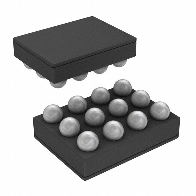
| 供应商器件封装 | 6-WLCSP(1.45x0.95) |
| 其它名称 | ADP197ACBZ-R7DKR |
| 包装 | Digi-Reel® |
| 商标 | Analog Devices |
| 安装类型 | 表面贴装 |
| 安装风格 | SMD/SMT |
| 导通电阻 | 12 毫欧 |
| 导通电阻—最大值 | 12 mOhms |
| 封装 | Reel |
| 封装/外壳 | 6-WFBGA,WLCSP |
| 封装/箱体 | WLCSP-6 |
| 工作温度 | -40°C ~ 85°C |
| 工作电源电压 | 1.8 V to 5.5 V |
| 工厂包装数量 | 3000 |
| 最大功率耗散 | 24 uW |
| 最大工作温度 | + 105 C |
| 最小工作温度 | - 40 C |
| 标准包装 | 1 |
| 电压-电源 | 1.8 V ~ 5.5 V |
| 电流-峰值输出 | - |
| 电流-输出/通道 | 3A |
| 类型 | 高端 |
| 系列 | ADP197 |
| 输入类型 | 非反相 |
| 输出数 | 1 |
| 输出电流 | 3 A |
| 输出端数量 | 1 Output |


- 商务部:美国ITC正式对集成电路等产品启动337调查
- 曝三星4nm工艺存在良率问题 高通将骁龙8 Gen1或转产台积电
- 太阳诱电将投资9.5亿元在常州建新厂生产MLCC 预计2023年完工
- 英特尔发布欧洲新工厂建设计划 深化IDM 2.0 战略
- 台积电先进制程称霸业界 有大客户加持明年业绩稳了
- 达到5530亿美元!SIA预计今年全球半导体销售额将创下新高
- 英特尔拟将自动驾驶子公司Mobileye上市 估值或超500亿美元
- 三星加码芯片和SET,合并消费电子和移动部门,撤换高东真等 CEO
- 三星电子宣布重大人事变动 还合并消费电子和移动部门
- 海关总署:前11个月进口集成电路产品价值2.52万亿元 增长14.8%


PDF Datasheet 数据手册内容提取
5 V, 3 A Logic Controlled High-Side Power Switch Data Sheet ADP197 FEATURES TYPICAL APPLICATIONS CIRCUIT Low RDS of 12 mΩ VIN VOUT ON + Low input voltage range: 1.8 V to 5.5 V – Quick output discharge (QOD) circuit (ADP197-02) GND 3 A continuous operating current at 70°C ON CHARGE PUMP 1.2 V logic-compatible enable input EN OFF AND SLEW RATE LOAD CONTROL Low 18 μA quiescent current, V < 3 V IN Low 31 μA quiescent current, V = 4.2 V IN Overtemperature protection UUllttrraalsomwa sllh 1u.0td momwn × c 1u.5rr menmt:, <01.5 μ mAm pitch, 6-ball WLCSP AODVPEPR1RT9OE7TMEPCETRIAOTNURE ADOPN19LY7-02 09298-001 Tiny 2.0 mm × 2.0 mm × 0.55 mm, 0.65 mm pitch, 6-lead LFCSP Figure 1. APPLICATIONS Mobile phones Digital cameras and audio devices Portable and battery-powered equipment GENERAL DESCRIPTION The ADP197 is a high-side load switch designed for operation The ADP197-02 incorporates an internal quick output between 1.8 V and 5.5 V. This load switch provides power domain discharge (QOD) circuit to discharge the output capacitance isolation, which helps extend battery operation. The device when the ADP197-02 output is disabled contains a low on-resistance, N-channel MOSFET that supports In addition to operating performance, the ADP197 WLCSP more than 3 A of continuous current and minimizes power loss. package occupies minimal printed circuit board (PCB) space The low 18 μA quiescent current and ultralow shutdown current with an area of less than 1.5 mm2 and a height of 0.60 mm. make the ADP197 ideal for battery-operated portable equipment. The ADP197 is available in an ultrasmall 1.0 mm × 1.5 mm, The built-in level shifter for enable logic makes the ADP197 0.5 mm pitch, 6-ball WLCSP and a 2.0 mm × 2.0 mm × compatible with many processors and GPIO controllers. 0.55 mm, 0.65 mm pitch, 6-lead LFCSP. Overtemperature protection circuitry activates if the junction temperature exceeds 125°C, thereby protecting itself and downstream circuits from potential damage. Rev. C Document Feedback Information furnished by Analog Devices is believed to be accurate and reliable. However, no responsibility is assumed by Analog Devices for its use, nor for any infringements of patents or other One Technology Way, P.O. Box 9106, Norwood, MA 02062-9106, U.S.A. rights of third parties that may result from its use. Specifications subject to change without notice. No license is granted by implication or otherwise under any patent or patent rights of Analog Devices. Tel: 781.329.4700 ©2011–2014 Analog Devices, Inc. All rights reserved. Trademarks and registered trademarks are the property of their respective owners. Technical Support www.analog.com
ADP197 Data Sheet TABLE OF CONTENTS Features .............................................................................................. 1 Typical Performance Characteristics ..............................................6 Applications ....................................................................................... 1 Theory of Operation ...................................................................... 10 Typical Applications Circuit ............................................................ 1 Applications Information .............................................................. 11 General Description ......................................................................... 1 Capacitor Selection .................................................................... 11 Revision History ............................................................................... 2 Ground Current .......................................................................... 11 Specifications ..................................................................................... 3 Enable Feature ............................................................................ 11 Timing Diagram ........................................................................... 3 Timing ......................................................................................... 12 Absolute Maximum Ratings ............................................................ 4 Outline Dimensions ....................................................................... 13 ESD Caution .................................................................................. 4 Ordering Guide .......................................................................... 13 Pin Configurations and Function Descriptions ........................... 5 REVISION HISTORY 10/14—Rev. B to Rev. C Added 6-lead LFCSP .......................................................... Universal Changes to Features Section, General Description Section, and Figure 1 ....................................................................................... 1 Changes to Table 1 ............................................................................ 3 Changes to Table 3 ............................................................................ 4 Added Figure 4 and Table 5; Renumbered Sequentially ............. 5 Added Figure 7 .................................................................................. 6 Changes to Figure 9 .......................................................................... 6 Changes to Figure 13 ........................................................................ 7 Changes to Theory of Operation Section .................................... 10 Changes to Figure 26 Caption ....................................................... 11 Changes to Figure 29 to Figure 33 and Timing Section ............ 12 Added Figure 35, Outline Dimensions ........................................ 13 Updated Outline Dimensions ....................................................... 13 Changes to Ordering Guide .......................................................... 13 5/12—Rev. A to Rev. B Changes to Ordering Guide .......................................................... 13 11/11—Rev. 0 to Rev. A Changed EN to GND Rating, Table 2 ............................................ 4 4/11—Revision 0: Initial Version Rev. C | Page 2 of 13
Data Sheet ADP197 SPECIFICATIONS V = 1.8 V, V = V , I = 1 A, T = 25°C, unless otherwise noted. IN EN IN OUT A Table 1. Parameter Symbol Test Conditions/Comments Min Typ Max Unit INPUT VOLTAGE RANGE V T = −40°C to +85°C 1.8 5.5 V IN J EN INPUT EN Input V V = 1.8 V to 5.5 V 1.2 V IH IN V V = 1.8 V to 5.5 V, T = −40°C to +85°C 0.4 V IL IN J V = 1.8 V to 5.5 V, T = −40°C to +110°C 0.35 V IN J EN Input Pull-Down Current I V = 1.8 V 500 nA EN IN CURRENT Ground Current I V = 1.8 V 18 μA GND IN V = 3.4 V 14 μA IN V = 4.2 V, T = −40°C to +110°C 18 31 μA IN J V = 5.5 V 28 μA IN Off State Current I V = GND, V = 0 V, V = 4.2 V 0.1 μA OFF EN OUT IN V = GND, T = −40°C to +85°C, V =0 V, V = 1.8 V to 5.5 V 20 μA EN J OUT IN V = GND, T = −40°C to +110°C, V =0 V, V = 1.8 V to 5.5 V 75 μA EN J OUT IN Continuous Operating Current1 I V = 1.8 V to 5.5 V 3 A OUT IN VIN TO VOUT RESISTANCE RDS ON WLCSP V = 5.5 V 0.012 Ω IN V = 4.2 V 0.012 Ω IN V = 1.8 V 0.012 Ω IN V = 1.8 V, T = −40°C to +85°C 0.012 0.017 Ω IN J LFCSP V = 5.5 V 0.027 Ω IN V = 4.2 V 0.027 Ω IN V = 1.8 V 0.027 Ω IN V = 1.8 V, T = −40°C to +85°C 0.027 0.036 Ω IN J V TURN-ON DELAY TIME See Figure 2 OUT Turn-On Delay Time t V = 1.8 V to 5.5 V, C = 1 μF 1 ms ON_DLY IN LOAD ACTIVE PULL-DOWN RESISTANCE R V = 3.2 V 380 Ω PULLDOWN IN (ADP197-02 OPTION ONLY) THERMAL SHUTDOWN Thermal Shutdown Threshold TS T rising 125 °C SD J Thermal Shutdown Hysteresis TS 15 °C SD-HYS 1 At an ambient temperature of 85°C, the device can withstand a continuous current of 2.22 A. At a load current of 3 A, the operational lifetime derates to 2190 hours. TIMING DIAGRAM VEN TURN-ON TURN-OFF DELAY DELAY 90% VOUT 10% TURNR-IOSNE TURNF-OAFLFL 09298-002 Figure 2. Timing Diagram Rev. C | Page 3 of 13
ADP197 Data Sheet ABSOLUTE MAXIMUM RATINGS Table 3. Typical θ and Ψ Values Table 2. JA JB Package Type θ Ψ Unit Parameter Rating JA JB 6-Ball, 0.5 mm Pitch WLCSP 260 58 °C/W VIN to GND −0.3 V to +6.5 V 6-Lead, 0.65 mm Pitch LFCSP 68.9 44.1 °C/W VOUT to GND −0.3 V to V IN EN to GND −0.3 V to +6.5 V Continuous Drain Current ESD CAUTION T = 25°C ±4 A A T = 85°C ±2.22 A A Continuous Diode Current −50 mA Storage Temperature Range −65°C to +150°C Operating Junction Temperature Range −40°C to +105°C Soldering Conditions JEDEC J-STD-020 Stresses above those listed under Absolute Maximum Ratings may cause permanent damage to the device. This is a stress rating only; functional operation of the device at these or any other conditions above those indicated in the operational section of this specification is not implied. Exposure to absolute maximum rating conditions for extended periods may affect device reliability. Rev. C | Page 4 of 13
Data Sheet ADP197 PIN CONFIGURATIONS AND FUNCTION DESCRIPTIONS 1 2 A VIN VOUT B VIN VOUT C EN GND ADP197 (NToOt Pto V SIEcaWle) 09298-003 Figure 3. 6-Ball WLCSP Pin Configuration Table 4. 6-Ball WLCSP Pin Function Descriptions Pin No. Mnemonic Description A1, B1 VIN Input Voltage. A2, B2 VOUT Output Voltage. C1 EN Enable Input. Drive EN high to turn on the switch and drive EN low to turn off the switch. C2 GND Ground. VOUT1 1 6 VIN1 ADP197 VOUT2 2 5 VIN2 TOP VIEW GND 3 4 EN N1 . O ETTXOEP SGORSOEUDN PDA.D MUST BE CONNECTED 09298-104 Figure 4. 6-Lead LFCSP Pin Configuration Table 5. 6-Lead LFCSP Pin Function Descriptions Pin No. Mnemonic Description 1 VOUT1 Output Voltage. Connect VOUT1 and VOUT2 together. 2 VOUT2 Output Voltage. Connect VOUT1 and VOUT2 together. 3 GND Ground. 4 EN Enable Input. Drive EN high to turn on the switch and drive EN low to turn off the switch. 5 VIN2 Input Voltage. Connect VIN1 and VIN2 together. 6 VIN1 Input Voltage. Connect VIN1 and VIN2 together. EP Exposed Pad. The exposed pad must be connected to ground. Rev. C | Page 5 of 13
ADP197 Data Sheet TYPICAL PERFORMANCE CHARACTERISTICS V = 1.8 V, V = V , C = C = 1 μF, T = 25°C, unless otherwise noted. IN EN IN IN OUT A 0.016 0.025 1.8V 50mA 3.4V 100mA 0.014 4.2V 200mA 5.5V 500mA 0.020 1000mA 0.012 3000mA 0.010 Ω) Ω)0.015 (ON0.008 (ON S S D D R R0.010 0.006 0.004 0.005 0.002 0 0 –40 –30 –20 –10 0 TE1M0PE2R0AT3U0RE 4(°0C)50 60 70 80 90 09298-004 1.0 1.5 2.0 2.5 3.V0IN (V3).5 4.0 4.5 5.0 5.5 09298-006 Figure 5. RDSON vs. Temperature, 500 mA Figure 8. RDSON vs. Input Voltage (VIN), Different Load Currents 0.016 0.050 1.8V 50mA 3.4V 0.045 100mA 0.014 4.2V 200mA 5.5V 500mA 0.040 1000mA 0.012 3000mA V)0.035 RDS (Ω)ON 00..001008 TAGE DROP (000...000223050 0.006 L O V0.015 0.004 0.010 0.002 0.005 0 0 –40 –30 –20 –10 0 TE1M0PE2R0AT3U0RE 4(°0C)50 60 70 80 90 09298-005 –40 –5 TEMPERA25TURE (°C) 65 85 09298-007 Figure 6. RDSON vs. Temperature, 3 A, Different Input Voltages (VIN) Figure 9. Voltage Drop vs. Temperature, Different Load Currents 0.040 50 100mA 1.8V 200mA 0.035 3.4V 45 500mA 4.2V 1000mA 5.5V 40 3000mA 0.030 µA) 35 (Ω)ON 00..002205 URRENT ( 2350 S C RD 0.015 UND 20 O R 15 0.010 G 10 0.005 5 0 0 –40–30–20–10 0 10TE2M0PE3R0AT4U0RE5 0(⁰C6)0 70 80 90 100110 09298-107 –40 –5 TEMPERA25TURE (°C) 65 85 09298-016 Figure 7. RDSON (LFCSP) vs. Temperature, 500 mA, Different Input Voltages (VIN) Figure 10. Ground Current vs. Temperature, Different Load Currents, VIN = 1.8 V Rev. C | Page 6 of 13
Data Sheet ADP197 50 0.50 100mA 1.8V 45 250000mmAA 0.45 12..95VV 1000mA 3.0V 40 3000mA A) 0.40 3.4V T (µA) 35 RENT (µ 0.35 3445....8260VVVV EN 30 UR 0.30 5.5V R C UR 25 N 0.25 C W D O N 20 D 0.20 GROU 15 SHUTD0.15 10 GN0.10 I 5 0.05 0 0 –40 –5TEMPERA2T5URE (°C) 65 85 09298-017 –40 –20 0 TEMP2E0RATUR4E0 (°C) 60 80 100 09298-020 Figure 11. Ground Current vs. Temperature, Different Load Currents, Figure 14. IGND Shutdown Current vs. Temperature, Output Open, VIN = 4.2 V Different Input Voltages (VIN) 50 10 100mA 1.8V 200mA 1.9V 45 500mA 2.5V 1000mA 3.0V 40 3000mA A) 3.4V T (µA) 35 RENT (µ 1 3445....8260VVVV EN 30 UR 5.5V R C CUR 25 WN ND 20 DO GROU 15 SHUTD 0.1 N 10 G I 5 0 –40 –5 TEMPERA25TURE (°C) 65 85 09298-018 0.01–40 –20 0 TEM2P0ERATU4R0E (°C) 60 80 100 09298-021 Figure 12. Ground Current vs. Temperature, Different Load Currents, Figure 15. IGND Shutdown Current vs. Temperature, VOUT = 0 V, VIN = 5.5 V Different Input Voltages (VIN) 50 1.8V 45 12..95VV ILOAD 3.0V 40 3.4V 3.8V ENT (µA) 3305 4455....2605VVVV 1 C20H41m AAMPL RR VOUT U 25 C ND 20 U O R 15 G 2 10 VEN 5 3 010 10L0OAD CURRENT (m1A0)00 10000 09298-019 CCHH13 120V0mA ΩBBWW CH2 1VBW MT 1 .1000.m20s% A CH3 1.28V 09298-008 Figure 13. Ground Current vs. Load Current, Different Input Voltages (VIN) Figure 16. Typical Turn-On Time and Inrush Current, VIN = 1.9 V, 200 mA Load Rev. C | Page 7 of 13
ADP197 Data Sheet ILOAD ILOAD 1 C1.H921A AMPL 1 VOUT C22H21m AAMPL VOUT 2 2 VEN VEN 3 3 CCHH13 12AV ΩBBWW CH2 1VBW MT 1 .1000.m00s% A CH3 1.28V 09298-009 CCHH13 120V0mA ΩBBWW CH2 2VBW MT 1 .1000.m00s% A CH3 1.28V 09298-012 Figure 17. Typical Turn-On Time and Inrush Current, VIN = 1.9 V, Figure 20. Typical Turn-On Time and Inrush Current, VIN = 5.5 V, 2 A Load 200 mA Load ILOAD ILOAD 1 C26H61m AAMPL 1 VOUT C2.H141A AMPL VOUT 2 2 VEN VEN 3 3 CCHH13 120V0mA ΩBBWW CH2 2VBW MT 1 .1000.m00s% A CH3 1.28V 09298-010 CCHH13 12AV ΩBBWW CH2 2VBW MT 1 .1000.m00s% A CH3 1.28V 09298-013 Figure 18. Typical Turn-On Time and Inrush Current, VIN = 1.9 V, Figure 21. Typical Turn-On Time and Inrush Current, VIN = 5.5 V, 200 mA Load, COUT = 100 μF 2 A Load ILOAD ILOAD 1 C1.H921A AMPL 1 VOUT C35H21m AAMPL VOUT 2 2 VEN VEN 3 3 CCHH13 12AV ΩBBWW CH2 2VBW MT 1 .1000.m00s% A CH3 1.28V 09298-011 CCHH13 220V0mA ΩBBWW CH2 2VBW MT 1 .1000.m00s% A CH3 1.28V 09298-014 Figure 19. Typical Turn-On Time and Inrush Current, VIN = 1.9 V, Figure 22. Typical Turn-On Time and Inrush Current, VIN = 5.5 V, 2 A Load, COUT = 100 μF 200 mA Load, COUT = 100 μF Rev. C | Page 8 of 13
Data Sheet ADP197 10 ILOAD A) 1 µ T ( N 1 VOUT C2.H121A AMPL RRE 0.1 U C N W DO 0.01 1.8V T 1.9V HU 2.5V 2 VEN SOUT 0.001 333...048VVV I 4.2V 4.6V 5.0V 3 5.5V CCHH13 12AV ΩBBWW CH2 2VBW MT 1 .1000.m00s% A CH3 1.28V 09298-015 0.0001–40 –20 0 TEMP2E0RATUR4E0 (°C) 60 80 100 09298-022 Figure 23. Typical Turn-On Time and Inrush Current, VIN = 5.5 V, Figure 24. IOUT Shutdown Current vs. Temperature, VOUT = 0 V, Different Input 2 A Load, COUT = 100 μF Voltages (VIN) Rev. C | Page 9 of 13
ADP197 Data Sheet THEORY OF OPERATION The ADP197 is capable of 3 A of continuous operating current VIN VOUT as long as T is less than 70°C. At 85°C, the rated current drops J to 2.22 A. GND CHARGE PUMP The overtemperature protection circuit activates if the load cur- EN AND SLEW RATE CONTROL rent causes the junction temperature to exceed 125°C. When this occurs, the overtemperature protection circuitry disables the output until the junction temperature falls below approximately OVERTEMPERATURE ADP197-02 110°C, at which point the output is reenabled. If the fault condition ADP1P9R7OTECTION ONLY 09298-023 pTehres iAstsD, Pth1e9 o7u-0tp2u itn ccyocrlepso orafft easn da QonO uDn tcili rtchue ifta tuolt d isis rcehmarogvee dth. e Figure 25. Functional Block Diagram output capacitance when the ADP197-02 output is disabled. The ADP197 is a high-side NMOS load switch, controlled by an ESD protection structures are shown in the block diagram as Zener internal charge pump. The ADP197 is designed to operate with diodes. power supply voltages between 1.8 V and 5.5 V. The ADP197 is a low quiescent current device with a nominal An internal charge pump biases the NMOS switch to achieve a 4 MΩ pull-down resistor on its EN pin. The package is a space- relatively constant, ultralow on resistance of 12 mΩ across the saving 1.0 mm × 1.5 mm, 0.5 mm pitch, 6-ball WLCSP and a entire input voltage range. The use of the internal charge pump tiny 2.0 mm × 2.0 mm × 0.55 mm, 0.65 mm pitch, 6-lead LFCSP. also allows for controlled turn-on times. Turning the NMOS switch on and off is controlled by the enable input pin (EN), which is capable of interfacing directly with 1.8 V logic signals. Rev. C | Page 10 of 13
Data Sheet ADP197 APPLICATIONS INFORMATION CAPACITOR SELECTION ENABLE FEATURE Output Capacitor The ADP197 uses the EN pin to enable and disable the VOUT pin under normal operating conditions. As shown in Figure 27, The ADP197 is designed for operation with small, space-saving when a rising voltage (V ) on the EN pin crosses the active ceramic capacitors but functions with most commonly used capa- EN threshold, VOUT turns on. When a falling voltage (V ) on citors when the effective series resistance (ESR) value is carefully EN the EN pin crosses the inactive threshold, VOUT turns off. considered. The ESR of the output capacitor affects the response to load transients. A typical 1 μF capacitor with an ESR of 0.1 Ω 4.0 VOUT AT 3.6V or less is recommended for good transient response. Using a larger 3.5 value of output capacitance improves the transient response to 3.0 large changes in load current. Input Bypass Capacitor 2.5 V) Connecting at least 1 μF of capacitance from VIN to GND reduces (UT 2.0 VEN FALLING VEN RISING O the circuit sensitivity to the printed circuit board (PCB) layout, V 1.5 especially when high source impedance or long input traces are encountered. When greater than 1 μF of output capacitance is 1.0 required, increase the input capacitor to match it. 0.5 GROUND CURRENT 0 Tchhaer gmea pjourm sopu frocre tfhoer gFrEoTun ddr icvuer rceirnctu init rtyh.e F AigDuPre1 9276 issh tohwe sin ttheer nal 0 0.2 0E.4NABLE V0O.6LTAGE (0V.)8 1.0 1.2 09298-025 Figure 27. Typical EN Operation typical ground current when V = V , and varies from 1.8 V EN IN to 5.5 V. As shown in Figure 27, the EN pin has hysteresis built into it. This built-in hysteresis prevents on/off oscillations that can 50 50mA occur due to noise on the EN pin as it passes through the 100mA 45 200mA threshold points. 500mA 40 1000mA µA) 35 3000mA The EN pin active and inactive thresholds derive from the VIN T ( voltage; therefore, these thresholds vary with the changing input EN 30 voltage. Figure 28 shows the typical EN active and inactive R R U 25 thresholds when the input voltage varies from 1.8 V to 5.5 V. C ND 20 1.2 U ENRISE RO 15 ENFALL G 1.0 10 5 (V) D 0.8 L 0 O 1.0 1.5 2.0 2.5 3.0VIN (V3).5 4.0 4.5 5.0 5.5 09298-024 THRESH 0.6 Figure 26. Ground Current vs. Input Voltage (VIN), Different Load Currents LE B 0.4 NA E 0.2 0 1.8 2.2 2.6 3.0INPU3T.4VOL3T.A8GE(4V.)2 4.6 5.0 5.4 09298-026 Figure 28. Typical EN Threshold vs. Input Voltage (VIN) Rev. C | Page 11 of 13
ADP197 Data Sheet TIMING ILOAD Turn-on delay is defined as the interval between the time that V exceeds the rising threshold voltage and when V rises to EN OUT ~10% of its final value. The ADP197 includes circuitry that has a typical 1 ms turn-on delay and a controlled rise time to limit the 1 C26H61m AAMPL V inrush current. As shown in Figure 29 and Figure 30, the turn- IN on delay is nearly independent of the input voltage. VOUT ILOAD 2 VEN CH1 AMPL 204mA 3 1 VOUT CCHH13 120V0mA ΩBBWW CH2 2VBW MT 1 .1000.m00s% A CH3 1.28V 09298-029 Figure 31. Typical Rise Time and Inrush Current, CLOAD = 100 μF, VIN = 1.9 V, ILOAD = 270 mA 2 VEN ILOAD 3 CCHH13 120V0mAΩBBWW CH2 1VBW MT 1 .1000.m20s% A CH3 1.28V 09298-027 1 VOUT C35H21m AAMPL Figure 29. Typical Turn-On Delay Time with VIN = 1.9 V, ILOAD = 200 mA ILOAD 2 VEN 1 VOUT C22H21m AAMPL 3 CCHH13 220V0mA ΩBBWW CH2 2VBW MT 1 .1000.m00s% A CH3 1.28V 09298-030 Figure 32. Typical Rise Time and Inrush Current, CLOAD = 100 μF, VIN = 5.5 V, ILOAD = 350 mA 2 VEN The turn-off time is defined as the time it takes for the output voltage to fall from 90% to 10% of V reaching its final value. It OUT is also dependent on the RC time constant of the output capacit- 3 CCHH13 120V0mA ΩBBWW CH2 2VBW MT 1 .1000.m00s% A CH3 1.28V 09298-028 atinmcee awnidth l oVaIdN =re 3si.s6t aVn, cCeO. UFTi g=u 1re μ 3F3, asnhdo wRsL OtAhDe =ty 1p8ic Ωal. turn-off Figure 30. Typical Turn-On Delay Time with VIN = 5.5 V, ILOAD = 220 mA The rise time is defined as the time it takes the output voltage to rise from 10% to 90% of V reaching its final value. It is depen- OUT 1 VEN dent on the rise time of the internal charge pump. For very large values of output capacitance, the RC time constant (where C is the load capacitance (C ) and R is the RDS ||R ) LOAD ON LOAD can become a factor in the rise time of the output voltage. Because RDS is much smaller than R , an adequate approximation ON LOAD for RC is RDS × C . An input or load capacitor is not ON LOAD required for the ADP197 although capacitors can be used to VOUT suppress noise on the board. Figure 31 and Figure 32 show the 2 inrush current when C is 100 μF. LOAD CH1 1V BW CH2 1VBW MT 2 020µ.s20% A CH1 240mV 09298-031 Figure 33. Typical Turn-Off Time Rev. C | Page 12 of 13
Data Sheet ADP197 OUTLINE DIMENSIONS 1.000 0.950 0.900 2 1 A BALLA1 IDENTIFIER 1.500 1.00 1.450 REF B 1.400 C 0.50 BSC TOP VIEW (BALL SIDE DOWN) 0.50 BSC 0.380 BOTTOM VIEW 0.675 0.355 (BALL SIDE UP) 0.595 SIDE VIEW 0.330 0.515 COPLANARITY 0.075 SEATING 0.345 0.270 PLANE 00..229455 00..224100 11-08-2012-B Figure 34. 6-Ball Wafer Level Chip Scale Package [WLCSP] (CB-6-2) Dimensions shown in millimeters 1.70 2.10 1.60 2.00 SQ 1.50 1.90 0.65 BSC 4 6 0.15 REF PIN 1 INDEX EXPOSED 1.10 AREA PAD 1.00 0.425 0.90 0.350 0.275 0.20 MIN 3 1 TOP VIEW BOTTOM VIEW PIN 1 INDICATOR (R 0.15) 0.60 0.55 0.05 MAX FTOHER EPXRPOOPSEERD C POANDN, ERCETFIEORN TOOF 0.50 0.02 NOM THE PIN CONFIGURATION AND FUNCTION DESCRIPTIONS SEPALTAINNGE 000...332505 0.20 REF SECTION OF THIS DATA SHEET. 02-06-2013-D Figure 35. 6-Lead Lead Frame Chip Scale Package [LFCSP_UD] 2.00 mm × 2.00 mm Body, Ultra Thin, Dual Lead (CP-6-3) Dimensions shown in millimeters ORDERING GUIDE Temperature Package On/Off Model1 Range Package Description Option Branding Time (μs) ADP197ACBZ-R7 −40°C to +85°C 6-Ball Wafer Level Chip Scale Package [WLCSP] CB-6-2 87 300 ADP197ACBZ-01-R7 −40°C to +85°C 6-Ball Wafer Level Chip Scale Package [WLCSP] CB-6-2 AP 20 ADP197ACPZN-01-R7 −40°C to +85°C 6-Lead Lead Frame Chip Scale Package [LFCSP_UD] CP-6-3 AP 20 ADP197ACPZN-02-R7 −40°C to +85°C 6-Lead Lead Frame Chip Scale Package [LFCSP_UD] CP-6-3 D8 20 ADP197CB-EVALZ Evaluation Board ADP197CP-EVALZ Evaluation Board 1 Z = RoHS Compliant Part. ©2011–2014 Analog Devices, Inc. All rights reserved. Trademarks and registered trademarks are the property of their respective owners. D09298-0-10/14(C) Rev. C | Page 13 of 13