ICGOO在线商城 > 集成电路(IC) > PMIC - 稳压器 - 线性 > ADP151AUJZ-1.8-R7
 Datasheet下载
- 型号: ADP151AUJZ-1.8-R7
- 制造商: Analog
- 库位|库存: xxxx|xxxx
- 要求:
| 数量阶梯 | 香港交货 | 国内含税 |
| +xxxx | $xxxx | ¥xxxx |
查看当月历史价格
查看今年历史价格
ADP151AUJZ-1.8-R7产品简介:
ICGOO电子元器件商城为您提供ADP151AUJZ-1.8-R7由Analog设计生产,在icgoo商城现货销售,并且可以通过原厂、代理商等渠道进行代购。 ADP151AUJZ-1.8-R7价格参考¥3.64-¥6.20。AnalogADP151AUJZ-1.8-R7封装/规格:PMIC - 稳压器 - 线性, Linear Voltage Regulator IC Positive Fixed 1 Output 200mA TSOT-5。您可以下载ADP151AUJZ-1.8-R7参考资料、Datasheet数据手册功能说明书,资料中有ADP151AUJZ-1.8-R7 详细功能的应用电路图电压和使用方法及教程。
ADP151AUJZ-1.8-R7是Analog Devices Inc.(亚德诺半导体)推出的一款高性能低噪声、低压差线性稳压器(LDO),输出电压固定为1.8V,采用小型5引脚TSOT封装。该器件适用于对电源噪声敏感、空间受限且需要高稳定性的便携式电子设备。

典型应用场景包括:
1. 便携式设备:广泛用于智能手机、平板电脑和可穿戴设备中,为微处理器、传感器和射频模块提供干净稳定的电源。
2. 电池供电系统:因其超低静态电流(典型值45μA)和低压差特性,适合电池供电应用,有效延长电池续航时间。
3. 射频与无线通信模块:优异的PSRR(电源抑制比,高达90dB)和低输出噪声(约9μVRMS)使其成为Wi-Fi、蓝牙、ZigBee等无线收发器的理想供电选择。
4. 精密模拟电路:可用于为ADC、DAC、传感器信号调理电路等对电源纹波敏感的模拟前端供电,确保信号精度。
5. 嵌入式系统与MCU供电:常用于为ARM Cortex-M系列等低功耗微控制器提供稳定核心电压。

ADP151AUJZ-1.8-R7具备过温保护和过流保护功能,工作温度范围为-40°C至+125°C,可靠性高,适合工业级和消费类电子产品。其无需外部补偿、输入电容即可稳定工作的设计,简化了电路布局,降低了整体成本与PCB面积占用,是高集成度、高性能电源管理方案中的优选器件。
| 参数 | 数值 |
| 产品目录 | 集成电路 (IC)半导体 |
| 描述 | IC REG LDO 1.8V 0.2A TSOT23-5线性稳压器 Ultra Low Noise 200mA CMOS |
| 产品分类 | |
| 品牌 | Analog Devices Inc |
| 产品手册 | |
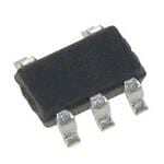
| 产品图片 |
|
| rohs | 符合RoHS无铅 / 符合限制有害物质指令(RoHS)规范要求 |
| 产品系列 | 电源管理 IC,线性稳压器,Analog Devices ADP151AUJZ-1.8-R7- |
| 数据手册 | |
| 产品型号 | ADP151AUJZ-1.8-R7 |
| 产品种类 | 线性稳压器 |
| 供应商器件封装 | TSOT-23-5 |
| 其它名称 | ADP151AUJZ-1.8-R7TR |
| 包装 | 带卷 (TR) |
| 商标 | Analog Devices |
| 安装类型 | 表面贴装 |
| 安装风格 | SMD/SMT |
| 封装 | Reel |
| 封装/外壳 | SOT-23-5 细型,TSOT-23-5 |
| 封装/箱体 | TSOT-5 |
| 工作温度 | -40°C ~ 125°C |
| 工厂包装数量 | 3000 |
| 最大工作温度 | + 125 C |
| 最大输入电压 | 5.5 V |
| 最小工作温度 | - 40 C |
| 最小输入电压 | 2.2 V |
| 标准包装 | 3,000 |
| 电压-跌落(典型值) | - |
| 电压-输入 | 2.2 V ~ 5.5 V |
| 电压-输出 | 1.8V |
| 电流-输出 | 200mA |
| 电流-限制(最小值) | 220mA |
| 稳压器拓扑 | 正,固定式 |
| 稳压器数 | 1 |
| 系列 | ADP151 |
| 视频文件 | http://www.digikey.cn/classic/video.aspx?PlayerID=1364138032001&width=640&height=505&videoID=2245193149001 |
| 输出电流 | 200 mA |


PDF Datasheet 数据手册内容提取
Ultralow Noise, 200 mA, CMOS Linear Regulator Data Sheet ADP151 FEATURES TYPICAL APPLICATION CIRCUIT Ultralow noise: 9 µV rms VIN = 2.3V VOUT = 1.8V 1 VIN VOUT 5 No noise bypass capacitor required 1µF 1µF Stable with 1 µF ceramic input and output capacitors 2 GND Maximum output current: 200 mA ON 3 EN NC 4 ILnopwu qt uvoieltsacgenet r acunrgree:n 2t. 2 V to 5.5 V OFF NC = NO CONNECT 08627-001 Figure 1. TSOT ADP151 with Fixed Output Voltage, 1.8 V I = 10 µA with 0 load GND I = 265 μA with 200 mA load GND 1 2 Low shutdown current: <1 µA LInoiwtia dl raocpcouurat cvyo: l±ta1g%e : 140 mV at 200 mA load VIN = C2.IN3V VINTOP VIEWVOUT A VOUC1Tµ O=FU 1T.8V Accuracy over line, load, and temperature: ±2.5% (Not to Scale) 1P6S RfiRx epde rofuotrpmuatn vcoel toafg 7e0 o dpBt iaotn 1s0: 1 k.H1 zV to 3.3 V OFF ON EN GND B 08627-002 Current-limit and thermal overload protection Figure 2. WLCSP ADP151 with Fixed Output Voltage, 1.8 V Logic controlled enable Internal pull-down resistor on EN input VIN = 2.3V 6 1 VOUT = 1.8V VIN VOUT 5-lead TSOT package 1µF ADP151 1µF 5 2 6-lead LFCSP package NCTOP VIEW NC ON 4 (Not to Scale) 3 4-ball, 0.4 mm pitch WLCSP OFF EN GND APPLICATIONS NCCO N=N NEOC TC OTONN TEHCIST .P DINO. NOT 08627-047 RF, VCO, and PLL power supplies Figure 3. LFCSP ADP151 with Fixed Output Voltage, 1.8 V Mobile phones Digital camera and audio devices Portable and battery-powered equipment Post dc-to-dc regulation Portable medical devices GENERAL DESCRIPTION The ADP151 is an ultralow noise, low dropout linear regulator The ADP151 is specifically designed for stable operation with that operates from 2.2 V to 5.5 V and provides up to 200 mA tiny 1 µF, ±30% ceramic input and output capacitors to meet of output current. The low 140 mV dropout voltage at 200 mA the requirements of high performance, space constrained load improves efficiency and allows operation over a wide input applications. voltage range. The ADP151 is capable of 16 fixed output voltage options, Using an innovative circuit topology, the ADP151 achieves ranging from 1.1 V to 3.3 V. ultralow noise performance without the necessity of a bypass Short-circuit and thermal overload protection circuits prevent capacitor, making it ideal for noise-sensitive analog and RF damage in adverse conditions. The ADP151 is available in tiny applications. The ADP151 also achieves ultralow noise per- 5-lead TSOT, 6-lead LFCSP, and 4-ball, 0.4 mm pitch, halide-free formance without compromising PSRR or transient line and WLCSP packages for the smallest footprint solution to meet a load performance. The low 265 μA of quiescent current at variety of portable power application requirements. 200 mA load makes the ADP151 suitable for battery-operated portable equipment. The ADP151 also includes an internal pull-down resistor on the EN input. Rev. E Information furnished by Analog Devices is believed to be accurate and reliable. However, no responsibility is assumed by Analog Devices for its use, nor for any infringements of patents or other One Technology Way, P.O. Box 9106, Norwood, MA 02062-9106, U.S.A. rights of third parties that may result from its use. Specifications subject to change without notice. No license is granted by implication or otherwise under any patent or patent rights of Analog Devices. Tel: 781.329.4700 www.analog.com Trademarks and registered trademarks are the property of their respective owners. Fax: 781.461.3113 ©2010–2012 Analog Devices, Inc. All rights reserved.
ADP151 Data Sheet TABLE OF CONTENTS Features .............................................................................................. 1 Typical Performance Characteristics ..............................................7 Applications ....................................................................................... 1 Theory of Operation ...................................................................... 11 Typical Application Circuit ............................................................. 1 Applications Information .............................................................. 12 General Description ......................................................................... 1 Capacitor Selection .................................................................... 12 Revision History ............................................................................... 2 Enable Feature ............................................................................ 13 Specifications ..................................................................................... 3 Adjustable Output Voltage Operation ..................................... 13 Input and Output Capacitor, Recommended Specifications .. 4 Current-Limit and Thermal Overload Protection ................. 15 Absolute Maximum Ratings ............................................................ 5 Thermal Considerations ............................................................ 15 Thermal Data ................................................................................ 5 Printed Circuit Board Layout Considerations ............................ 20 Thermal Resistance ...................................................................... 5 Outline Dimensions ....................................................................... 21 ESD Caution .................................................................................. 5 Ordering Guide .......................................................................... 22 Pin Configurations and Function Descriptions ........................... 6 REVISION HISTORY 4/12—Rev. D to Rev. E Added Figure 51 to Figure 56 ....................................................... 18 Changes to Figure 33 ...................................................................... 13 Added Figure 59 ............................................................................. 19 Updated Outline Dimensions ....................................................... 21 Added Figure 62 ............................................................................. 20 Changes to Ordering Guide .......................................................... 22 Added Figure 65 ............................................................................. 21 Updated Outline Dimensions ....................................................... 21 3/11—Rev. C to Rev. D Changes to Ordering Guide .......................................................... 23 Changes to Current-Limit Threshold Temperature Range ......... 4 Added EPAD Notation .................................................................... 6 8/10—Rev. 0 to Rev. A Changes to Ordering Guide .......................................................... 22 Changes to Figure 8 ........................................................................... 7 Changes to Figure 15 Caption and Figure 16 Caption ................. 8 1/11—Rev. B to Rev. C Changes to Figure 17 Caption and Figure 18 Caption ................. 9 Changes to Figure 23 ........................................................................ 9 Changes to Ordering Guide .......................................................... 21 12/10—Rev. A to Rev. B 3/10—Revision 0: Initial Version Added LFCSP Package ....................................................... Universal Added Figure 3; Renumbered Sequentially .................................. 1 Added Table 2 Caption; Renumbered Sequentially ..................... 4 Changes to Table 4 ............................................................................ 5 Added Figure 6, Changes to Table 5 ............................................... 6 Changes to Figure 23 ........................................................................ 9 Changes to Figure 37 and Figure 38 ............................................. 14 Rev. E | Page 2 of 24
Data Sheet ADP151 SPECIFICATIONS V = (V + 0.4 V) or 2.2 V, whichever is greater; EN = V , I = 10 mA, C = C = 1 µF, T = 25°C, unless otherwise noted. IN OUT IN OUT IN OUT A Table 1. Parameter Symbol Conditions Min Typ Max Unit INPUT VOLTAGE RANGE V T = −40°C to +125°C 2.2 5.5 V IN J OPERATING SUPPLY CURRENT I I = 0 µA 10 µA GND OUT I = 0 µA, T = −40°C to +125°C 20 µA OUT J I = 100 µA 20 µA OUT I = 100 µA, T = −40°C to +125°C 40 µA OUT J I = 10 mA 60 µA OUT I = 10 mA, T = −40°C to +125°C 90 µA OUT J I = 200 mA 265 μA OUT I = 200 mA, T = −40°C to +125°C 350 μA OUT J SHUTDOWN CURRENT I EN = GND 0.2 µA GND-SD EN = GND, T = −40°C to +125°C 1.0 µA J OUTPUT VOLTAGE ACCURACY V I = 10 mA −1 +1 % OUT OUT TSOT/LFCSP V T = −40°C to +125°C OUT J V < 1.8 V OUT 100 µA < I < 200 mA, V = (V + 0.4 V) to 5.5 V −3 +2 % OUT IN OUT V ≥1.8 V OUT 100 µA < I < 200 mA, V = (V + 0.4 V) to 5.5 V −2.5 +1.5 % OUT IN OUT WLCSP V T = −40°C to +125°C OUT J V < 1.8 V OUT 100 µA < I < 200 mA, V = (V + 0.4 V) to 5.5 V −2.5 +2 % OUT IN OUT V ≥1.8 V OUT 100 µA < I < 200 mA, V = (V + 0.4 V) to 5.5 V −2 +1.5 % OUT IN OUT REGULATION Line Regulation ∆V /∆V V = (V + 0.4 V) to 5.5 V, T = −40°C to +125°C −0.05 +0.05 %/V OUT IN IN OUT J Load Regulation (TSOT/LFCSP)1 ∆V /∆I V < 1.8 V %/mA OUT OUT OUT I = 100 µA to 200 mA 0.006 %/mA OUT I = 100 µA to 200 mA, T = −40°C to +125°C 0.012 %/mA OUT J V ≥ 1.8 V OUT I = 100 µA to 200 mA 0.003 %/mA OUT I = 100 µA to 200 mA, T = −40°C to +125°C 0.008 %/mA OUT J Load Regulation (WLCSP)1 ∆V /∆I V < 1.8 V %/mA OUT OUT OUT I = 100 µA to 200 mA 0.004 %/mA OUT I = 100 µA to 200 mA, T = −40°C to +125°C 0.009 %/mA OUT J V ≥1.8 V OUT I = 100 µA to 200 mA 0.002 %/mA OUT I = 100 µA to 200 mA, T = −40°C to +125°C 0.006 %/mA OUT J DROPOUT VOLTAGE2 V I = 10 mA 10 mV DROPOUT OUT I = 10 mA, T = −40°C to +125°C 30 mV OUT J TSOT/LFCSP I = 200 mA 150 mV OUT I = 200 mA, T = −40°C to +125°C 230 mV OUT J WLCSP I = 200 mA 135 mV OUT I = 200 mA, T = −40°C to +125°C 200 mV OUT J Rev. E | Page 3 of 24
ADP151 Data Sheet Parameter Symbol Conditions Min Typ Max Unit START-UP TIME3 t V = 3.3 V 180 µs START-UP OUT CURRENT-LIMIT THRESHOLD4 I T = 0°C to +125°C 220 300 400 mA LIMIT J UNDERVOLTAGE LOCKOUT T = −40°C to +125°C J Input Voltage Rising UVLO 1.96 V RISE Input Voltage Falling UVLO 1.28 V FALL Hysteresis UVLO 120 mV HYS THERMAL SHUTDOWN Thermal Shutdown Threshold TSSD TJ rising 150 °C Thermal Shutdown Hysteresis TSSD-HYS 15 °C EN INPUT EN Input Logic High V 2.2 V ≤ V ≤ 5.5 V 1.2 V IH IN EN Input Logic Low V 2.2 V ≤ V ≤ 5.5 V 0.4 V IL IN EN Input Pull-Down Resistance R V = V = 5.5 V 2.6 MΩ EN IN EN OUTPUT NOISE OUT 10 Hz to 100 kHz, V = 5 V, V = 3.3 V 9 µV rms NOISE IN OUT 10 Hz to 100 kHz, V = 5 V, V = 2.5 V 9 µV rms IN OUT 10 Hz to 100 kHz, V = 5 V, V = 1.1 V 9 µV rms IN OUT POWER SUPPLY REJECTION RATIO PSRR V = V + 0.5 V 10 kHz, V = 3.8 V, V = 3.3 V, I = 10 mA 70 dB IN OUT IN OUT OUT 100 kHz, V = 3.8 V, V = 3.3 V, I = 10 mA 55 dB IN OUT OUT V = V + 1 V 10 kHz, V = 4.3 V, V = 3.3 V, I = 10 mA 70 dB IN OUT IN OUT OUT 100 kHz, V = 4.3 V, V = 3.3 V, I = 10 mA 55 dB IN OUT OUT 10 kHz, V = 2.2 V, V = 1.1 V, I = 10 mA 70 dB IN OUT OUT 100 kHz, V = 2.2 V, V = 1.1 V, I = 10 mA 55 dB IN OUT OUT 1 Based on an end-point calculation using 0.1 mA and 200 mA loads. See Figure 8 for typical load regulation performance for loads less than 1 mA. 2 Dropout voltage is defined as the input-to-output voltage differential when the input voltage is set to the nominal output voltage. This applies only for output voltages above 2.2 V. 3 Start-up time is defined as the time between the rising edge of EN and VOUT being at 90% of its nominal value. 4 Current-limit threshold is defined as the current at which the output voltage drops to 90% of the specified typical value. For example, the current limit for a 3.0 V output voltage is defined as the current that causes the output voltage to drop to 90% of 3.0 V (that is, 2.7 V). INPUT AND OUTPUT CAPACITOR, RECOMMENDED SPECIFICATIONS Table 2. Parameter Symbol Conditions Min Typ Max Unit Minimum Input and Output C T = −40°C to +125°C 0.7 µF MIN A Capacitance1 Capacitor ESR R T = −40°C to +125°C 0.001 0.2 Ω ESR A 1 The minimum input and output capacitance should be greater than 0.7 μF over the full range of operating conditions. The full range of operating conditions in the application must be considered during device selection to ensure that the minimum capacitance specification is met. X7R and X5R type capacitors are recommended; Y5V and Z5U capacitors are not recommended for use with any LDO. Rev. E | Page 4 of 24
Data Sheet ADP151 ABSOLUTE MAXIMUM RATINGS on PCB material, layout, and environmental conditions. The Table 3. specified values of θ are based on a 4-layer, 4 in. × 3 in. circuit JA Parameter Rating board. See JESD51-7 and JESD51-9 for detailed information VIN to GND −0.3 V to +6.5 V on the board construction. For additional information, see the VOUT to GND −0.3 V to VIN AN-617 Application Note, MicroCSP™ Wafer Level Chip Scale EN to GND −0.3 V to +6.5V Package, available at www.analog.com. Storage Temperature Range −65°C to +150°C Ψ is the junction-to-board thermal characterization parameter Operating Junction Temperature Range −40°C to +125°C JB with units of °C/W. Ψ of the package is based on modeling and Operating Ambient Temperature Range −40°C to +125°C JB calculation using a 4-layer board. The JESD51-12, Guidelines for Soldering Conditions JEDEC J-STD-020 Reporting and Using Electronic Package Thermal Information, states Stresses above those listed under absolute maximum ratings that thermal characterization parameters are not the same as may cause permanent damage to the device. This is a stress thermal resistances. Ψ measures the component power flowing JB rating only and functional operation of the device at these or through multiple thermal paths rather than a single path as in any other conditions above those indicated in the operational thermal resistance, θ . Therefore, Ψ thermal paths include JB JB section of this specification is not implied. Exposure to absolute convection from the top of the package as well as radiation from maximum rating conditions for extended periods may affect the package, factors that make Ψ more useful in real-world JB device reliability. applications. Maximum junction temperature (T) is calculated J THERMAL DATA from the board temperature (TB) and power dissipation (PD) using the formula Absolute maximum ratings apply individually only, not in combination. The ADP151 can be damaged when the junction TJ = TB + (PD × ΨJB) temperature limits are exceeded. Monitoring ambient temperature See JESD51-8 and JESD51-12 for more detailed information does not guarantee that TJ is within the specified temperature about ΨJB. limits. In applications with high power dissipation and poor thermal resistance, the maximum ambient temperature may THERMAL RESISTANCE have to be derated. θ and Ψ are specified for the worst-case conditions, that is, a JA JB In applications with moderate power dissipation and low PCB device soldered in a circuit board for surface-mount packages. thermal resistance, the maximum ambient temperature can exceed the maximum limit as long as the junction temperature Table 4. Thermal Resistance is within specification limits. The junction temperature (TJ) of Package Type θJA ΨJB Unit the device is dependent on the ambient temperature (T ), the 5-Lead TSOT 170 43 °C/W A power dissipation of the device (P ), and the junction-to-ambient 4-Ball, 0.4 mm Pitch WLCSP 260 58 °C/W D thermal resistance of the package (θ ). 6-Lead 2 mm × 2 mm LFCSP 63.6 28.3 °C/W JA The maximum junction temperature (T) is calculated from the J ESD CAUTION ambient temperature (T ) and power dissipation (P ) using the A D formula T = T + (P × θ ) J A D JA The junction-to-ambient thermal resistance (θ ) of the package JA is based on modeling and calculation using a 4-layer board. The junction-to-ambient thermal resistance is highly dependent on the application and board layout. In applications where high maximum power dissipation exists, close attention to thermal board design is required. The value of θ may vary, depending JA Rev. E | Page 5 of 24
ADP151 Data Sheet PIN CONFIGURATIONS AND FUNCTION DESCRIPTIONS 1 2 VOUT1 6 VIN VIN 1 5 VOUT ADP151 ADP151 GNEDN N23C (=NT oNOtO Pto CV SOIEcNaWNleE)CT4 NC 08627-003 AB VEIN(NNToOt Pto V SIEcaWVGlOeN)UDT 08627-004 N12..O NTTHCEE S= ENXOP OCGOSNNECNDDN23 EPCATD. M(DNOTUoOS tN PTtOo VB TSIE EcC WaCOlOeN)NNNEECCT54T TENEODNC TTHO08627-048I SG PRIONU.ND. Figure 4. 5-Lead TSOT Pin Configuration Figure 5. 4-Ball WLCSP Pin Configuration Figure 6. 6-Lead LFCSP Pin Configuration Table 5. Pin Function Descriptions Pin No. TSOT WLCSP LFCSP Mnemonic Description 1 A1 6 VIN Regulator Input Supply. Bypass VIN to GND with a 1 µF or greater capacitor. 2 B2 3 GND Ground. 3 B1 4 EN Enable Input. Drive EN high to turn on the regulator; drive EN low to turn off the regulator. For automatic startup, connect EN to VIN. 4 N/A 2 NC No Connect. Not connected internally. 5 A2 1 VOUT Regulated Output Voltage. Bypass VOUT to GND with a 1 µF or greater capacitor. N/A N/A 5 NC No Connect. Not connected internally. N/A N/A EPAD Exposed Pad. The exposed pad must be connected to ground. The exposed pad enhances the thermal performance of the package. Rev. E | Page 6 of 24
Data Sheet ADP151 TYPICAL PERFORMANCE CHARACTERISTICS V = 5 V, V = 3.3 V, I = 1 mA, C = C = 1 µF, T = 25°C, unless otherwise noted. IN OUT OUT IN OUT A 3.35 1k 3.33 A) µ T ( 100 V) 3.31 REN (OUT CUR V D 3.29 N U LOAD = 10µA RO 10 LOAD = 100µA G LOAD = 10µA LOAD = 100µA 3.27 LOAD = 1mA LOAD = 1mA LOAD = 10mA LOAD = 10mA LOAD = 100mA LOAD = 100mA LOAD = 200mA LOAD = 200mA 3.25 –40 JU–N5CTION TEM2P5ERATURE 8(5°C) 125 08627-005 1 –40 JU–N5CTION TEM2P5ERATURE 8(5°C) 125 08627-008 Figure 7. Output Voltage vs. Junction Temperature Figure 10. Ground Current vs. Junction Temperature 3.35 1k 3.33 A) µ T ( V) 3.31 REN (OUT CUR 100 V D 3.29 N U O R G 3.27 3.25 10 0.01 0.1 1ILOAD (mA)10 100 1000 08627-006 0.01 0.1 1ILOAD (mA)10 100 1000 08627-009 Figure 8. Output Voltage vs. Load Current Figure 11. Ground Current vs. Load Current 3.35 1k LOAD = 10µA LOAD = 10mA LOAD = 100µA LOAD = 100mA LOAD = 1mA LOAD = 200mA 3.33 A) µ T ( V) 3.31 REN (OUT CUR 100 V D 3.29 N U O R LOAD = 10µA G LOAD = 100µA 3.27 LOAD = 1mA LOAD = 10mA LOAD = 100mA LOAD = 200mA 3.25 10 3.6 3.8 4.0 4.2 4.4VIN 4(.V6) 4.8 5.0 5.2 5.4 08627-007 3.6 3.8 4.0 4.2 4.4VIN 4(.V6) 4.8 5.0 5.2 5.4 08627-010 Figure 9. Output Voltage vs. Input Voltage Figure 12. Ground Current vs. Input Voltage Rev. E | Page 7 of 24
ADP151 Data Sheet 0.45 800 VIN = 3.6V IOUT = 1mA 0.40 VVIINN == 34..82VV 700 IIOOUUTT == 51m0mAA ENT (µA) 00..3350 VVVIIINNN === 445...485VVV NT (µA) 650000 IIIOOOUUUTTT === 512000m00mmAAA R E R 0.25 R U R C U 400 WN 0.20 D C UTDO 0.15 ROUN 300 SH 0.10 G 200 0.05 100 0–50 –25 0 TE2M5PERAT5U0RE (°C7)5 100 125 08627-011 03.10 3.15 3.20 3.25 3.3V0IN (3V.)35 3.40 3.45 3.50 3.55 08627-014 Figure 13. Shutdown Current vs. Temperature at Various Input Voltages Figure 16. Ground Current vs. Input Voltage (in Dropout) 120 0 200mA –10 100mA 10mA 100 –20 1mA A) 100µA m –30 E ( 80 AG B) –40 OLT 60 R (d –50 V R UT PS –60 O ROP 40 –70 D –80 20 –90 01 10 ILOAD (mA) 100 1000 08627-012 –10010 100 1kFREQU1E0NkCY (Hz1)00k 1M 10M 08627-015 Figure 14. Dropout Voltage vs. Load Current Figure 17. Power Supply Rejection Ratio vs. Frequency, VOUT = 1.2 V, VIN = 2.2 V 3.40 0 200mA –10 100mA 3.35 10mA –20 1mA 3.30 100µA –30 3.25 V (V)OUT 3.20 PSRR (dB) –––456000 3.15 IOUT = 1mA –70 3.10 IOUT = 5mA IOUT = 10mA –80 3.05 IOUT = 50mA IOUT = 100mA –90 IOUT = 200mA 3.003.10 3.15 3.20 3.25 3.3V0IN (3V.)35 3.40 3.45 3.50 3.55 08627-013 –10010 100 1kFREQU1E0NkCY (Hz1)00k 1M 10M 08627-016 Figure 15. Output Voltage vs. Input Voltage (in Dropout) Figure 18. Power Supply Rejection Ratio vs. Frequency, VOUT = 2.8 V, VIN = 3.3 V Rev. E | Page 8 of 24
Data Sheet ADP151 0 14 200mA 3.3V –10 100mA 13 2.8V 10mA 12 1.2V –20 1mA 11 1.1V 100µA –30 10 s) 9 RR (dB) ––4500 E (µV rm 78 PS –60 OIS 6 N 5 –70 4 –80 3 2 –90 1 –10010 100 1kFREQU1E0NkCY (Hz1)00k 1M 10M 08627-017 00.001 0.01 0L.1OAD CUR1RENT (mA10) 100 1k 08627-020 Figure 19. Power Supply Rejection Ratio vs. Frequency, VOUT = 3.3 V, VIN = 3.8 V Figure 22. Output Noise vs. Load Current and Output Voltage, VIN = 5 V, COUT = 1 μF 0 1000 VOUT = 3.3V, IOUT = 200mA 3.3V –10 VOUT = 3.3V, IOUT = 10mA 2.8V –20 VVVOOOUUUTTT === 221...881VVV,,, IIIOOOUUUTTT === 2120000m0mmAAA nV/Hz) 11..21VV –30 VOUT = 1.1V, IOUT = 10mA Y ( T B) –40 NSI RR (d –50 AL DE 100 S R P –60 T C E –70 SP E S –80 OI N –90 –10010 100 1kFREQU1E0NkCY (Hz1)00k 1M 10M 08627-018 1010 100 FREQUE1kNCY (Hz) 10k 100k 08627-021 Figure 20. Power Supply Rejection Ratio vs. Frequency at Various Output Voltages Figure 23. Output Noise Spectral Density vs. Frequency, and Load Currents, VOUT − VIN = 0.5 V, except for VOUT = 1.1 V, VIN = 2.2 V VIN = 5 V, ILOAD = 10 mA, COUT = 1 μF 0 T IOUT = 200mA, VIN = 3.3V LOAD CURRENT –10 IOUT = 10mA, VIN =3.3V IOUT = 200mA, VIN = 3.8V –20 IOUT = 10mA, VIN = 3.8V 1 –30 B) –40 d R ( –50 R S P –60 2 –70 VOUT –80 –90 –10010 100 1kFREQU1E0NkCY (Hz1)00k 1M 10M 08627-019 CH1 200mA CH2 50mV MT 2 0 1µ0s.00% A CH1 64.0mA 08627-022 Figure 21. Power Supply Rejection Ratio vs. Frequency at Various Voltages Figure 24. Load Transient Response, CIN, COUT = 1 μF, ILOAD = 1 mA to 200 mA and Load Currents, VOUT = 2.8 V Rev. E | Page 9 of 24
ADP151 Data Sheet T T INPUT VOLTAGE INPUT VOLTAGE 2 2 VOUT VOUT 1 1 CH1 1V CH2 2mV MT 1 0 1µ0s.80% A CH1 4.56V 08627-023 CH1 1V CH2 2mV MT 1 0 1µ0s.80% A CH1 4.56V 08627-024 Figure 25. Line Transient Response, CIN, COUT = 1 μF, ILOAD = 200 mA Figure 26. Line Transient Response, CIN, COUT = 1 μF, ILOAD = 1 mA Rev. E | Page 10 of 24
Data Sheet ADP151 THEORY OF OPERATION The ADP151 is an ultralow noise, low quiescent current, low Internally, the ADP151 consists of a reference, an error amplifier, a dropout linear regulator that operates from 2.2 V to 5.5 V and feedback voltage divider, and a PMOS pass transistor. Output can provide up to 200 mA of output current. Drawing a low current is delivered via the PMOS pass device, which is controlled 265 μA of quiescent current (typical) at full load makes the by the error amplifier. The error amplifier compares the reference ADP151 ideal for battery-operated portable equipment. voltage with the feedback voltage from the output and amplifies Shutdown current consumption is typically 200 nA. the difference. If the feedback voltage is lower than the reference voltage, the gate of the PMOS device is pulled lower, allowing Using new innovative design techniques, the ADP151 provides more current to pass and increasing the output voltage. If the superior noise performance for noise-sensitive analog and RF feedback voltage is higher than the reference voltage, the gate of applications without the need for a noise bypass capacitor. The the PMOS device is pulled higher, allowing less current to pass ADP151 is also optimized for use with small 1 µF ceramic and decreasing the output voltage. capacitors. An internal pull-down resistor on the EN input holds the input VIN VOUT low when the pin is left open. The ADP151 is available in 16 output voltage options, ranging R1 from 1.1 V to 3.3 V. The ADP151 uses the EN pin to enable and GND SHUOVRLTO-C, IARNCDUIT, disable the VOUT pin under normal operating conditions. When THERMAL PROTECT EN is high, VOUT turns on; when EN is low, VOUT turns off. For automatic startup, EN can be tied to VIN. EN SHUTDOWN R2 REN REFERENCE 08627-025 Figure 27. Internal Block Diagram Rev. E | Page 11 of 24
ADP151 Data Sheet APPLICATIONS INFORMATION CAPACITOR SELECTION Figure 29 depicts the capacitance vs. voltage bias characteristic of an 0402, 1 µF, 10 V X5R capacitor. The voltage stability of a Output Capacitor capacitor is strongly influenced by the capacitor size and voltage The ADP151 is designed for operation with small, space-saving rating. In general, a capacitor in a larger package or higher voltage ceramic capacitors but can function with most commonly used rating exhibits better stability. The temperature variation of the capacitors as long as care is taken with regard to the effective X5R dielectric is ~±15% over the −40°C to +85°C temperature series resistance (ESR) value. The ESR of the output capacitor range and is not a function of package or voltage rating. affects the stability of the LDO control loop. A minimum of 1 µF 1.2 capacitance with an ESR of 1 Ω or less is recommended to ensure the stability of the ADP151. Transient response to changes in load 1.0 current is also affected by output capacitance. Using a larger value of output capacitance improves the transient response of the F) 0.8 µ ADP151 to large changes in load current. Figure 28 shows the E ( C transient responses for an output capacitance value of 1 µF. N A 0.6 T CI T A LOAD CURRENT CAP 0.4 1 0.2 00 2 V4OLTAGE BIA6S 8 10 08627-027 2 Figure 29. Capacitance vs. Voltage Bias Characteristic VOUT Use Equation 1 to determine the worst-case capacitance, accounting for capacitor variation over temperature, component tolerance, and voltage. CH1 200mA CH2 50mV MT 2 0 1µ0s.00% A CH1 64mA 08627-026 wherCe:E FF = CBIAS × (1 − TEMPCO) × (1 − TOL) (1) Figure 28. Output Transient Response, COUT = 1 µF C is the effective capacitance at the operating voltage. BIAS Input Bypass Capacitor TEMPCO is the worst-case capacitor temperature coefficient. Connecting a 1 µF capacitor from VIN to GND reduces TOL is the worst-case component tolerance. the circuit sensitivity to the printed circuit board (PCB) layout, In this example, the worst-case temperature coefficient (TEMPCO) especially when long input traces or high source impedance over −40°C to +85°C is assumed to be 15% for an X5R dielectric. are encountered. If greater than 1 µF of output capacitance is The tolerance of the capacitor (TOL) is assumed to be 10%, and required, the input capacitor should be increased to match it. C is 0.94 μF at 1.8 V, as shown in Figure 29. BIAS Input and Output Capacitor Properties Substituting these values in Equation 1 yields Any good quality ceramic capacitor can be used with the CEFF = 0.94 μF × (1 − 0.15) × (1 − 0.1) = 0.719 μF ADP151, as long as it meets the minimum capacitance and Therefore, the capacitor chosen in this example meets the maximum ESR requirements. Ceramic capacitors are manufac- minimum capacitance requirement of the LDO over tempera- tured with a variety of dielectrics, each with different behavior ture and tolerance at the chosen output voltage. over temperature and applied voltage. Capacitors must have an To guarantee the performance of the ADP151, it is imperative adequate dielectric to ensure the minimum capacitance over the that the effects of dc bias, temperature, and tolerances on the necessary temperature range and dc bias conditions. X5R or X7R behavior of the capacitors be evaluated for each application. dielectrics with a voltage rating of 6.3 V or 10 V are recommended. Y5V and Z5U dielectrics are not recommended, due to their poor temperature and dc bias characteristics. Rev. E | Page 12 of 24
Data Sheet ADP151 ENABLE FEATURE 3.5 The ADP151 uses the EN pin to enable and disable the VOUT 3.0 pin under normal operating conditions. As shown in Figure 30, when a rising voltage on EN crosses the active threshold, VOUT 2.5 E G turns on. When a falling voltage on EN crosses the inactive A LT 2.0 threshold, VOUT turns off. O V E 3.0 BL 1.5 A N E 2.5 1.0 ENABLE 0.5 3.3V 2.0 2.8V 1.1V VOUT 1.5 00 50 100 150 2T0I0ME (2µ5s0) 300 350 400 450 08627-030 Figure 32. Typical Start-Up Behavior 1.0 ADJUSTABLE OUTPUT VOLTAGE OPERATION 0.5 The unique architecture of the ADP151 makes an adjustable version difficult to implement in silicon. However, it is possible 00 0.5 EN1A.0BLE VOLT1A.5GE 2.0 2.5 08627-028 tqou icersecaetne ta cnu ardrejunstt oabf lteh ere rgeuglualtaotro ar tc tihrceu eixt.p ense of increasing the Figure 30. ADP151 Typical EN Pin Operation The ADP151, and similar LDOs, are designed to regulate the As shown in Figure 30, the EN pin has hysteresis built in. This output voltage, V , appearing at the VOUT pin with respect OUT prevents on/off oscillations that can occur due to noise on the to the GND pin. If the GND pin is at a potential other than 0 V EN pin as it passes through the threshold points. (for example, at V ), the ADP151 output voltage is V + OFFSET OUT V . By taking advantage of this behavior, it is possible to The EN pin active/inactive thresholds are derived from the VIN OFFSET create an adjustable ADP151 circuit that retains most of the voltage. Therefore, these thresholds vary with changing input desirable characteristics of the ADP151. voltage. Figure 31 shows typical EN active/inactive thresholds when the input voltage varies from 2.2 V to 5.5 V. VIN VOUT 1 VIN VOUT 5 1200 C1 U1 C2 2 GND 1000 3 EN NC 4 VOFFSET E VOLTAGE 860000 VVEENN FRAISLEL Figure 3R32. AdjustaCb3VlOeU LTD =O V ULDsOin ×Rg (1 1th +e R A2D/RP11)5108627-131 L B ENA 400 The circuit shown in Figure 33 is an example of an adjustable LDO using the ADP151. A stable V voltage is created by OFFSET passing a known current through R2. The current through R2 is 200 determined by the voltage across R1. Because the voltage across R1 is set by the voltage between VOUT and GND, the current 02.0 2.5 3.0 INP3U.5T VOLT4.A0GE 4.5 5.0 5.5 08627-029 passing through R2 is fixed, and VOFFSET is stable. Figure 31. Typical EN Pin Thresholds vs. Input Voltage To minimize the effect variation of the ADP151 ground current (I ) with load, it is best to keep R1 as small as possible. It is GND The ADP151 uses an internal soft start to limit the inrush current also best to size the current passing through R2 to at least 20× when the output is enabled. The start-up time for the 3.3 V greater than the maximum expected ground current. option is approximately 160 μs from the time the EN active threshold is crossed to when the output reaches 90% of its final To create a 4 V LDO circuit, start with the 3.3 V version of the value. As shown in Figure 32, the start-up time is dependent on ADP151 to minimize the value of R2. Because VOUT is 4 V, the output voltage setting. VOFFSET must be 0.7 V, and the current through R2 must be 7 mA. R1 is, therefore, 3.3 V/7 mA or 471 Ω. A 470 Ω standard value introduces less than 1% error. Capacitor C3 is necessary to stabilize the LDO; a value of 1 μF is adequate. Rev. E | Page 13 of 24
ADP151 Data Sheet Figure 34 through Figure 38 show the typical performance of the 11 4 V LDO circuit. The noise performance of the 4 V LDO circuit is only about 1 μV worse than the same LDO used at 3.3 V because the output noise of 10 the circuit is almost solely determined by the LDO and not the ms) external components. The small difference may be attributed to the V r µ internally generated noise in the LDO ground current working with SE ( OI R2. By keeping R2 small, this noise contribution can be minimized. N 9 The PSRR of the 4 V circuit is as much as 10 dB poorer than the 3.3 V LDO with 500 mV of headroom because the ground current of the LDO varies slightly with input voltage. This, in turn, imncordeualsaintegs tVhOeF hFSeETa danrodo rmed tuoc 1e sV t,h teh eP SPRSRRR o fp tehrefo rremgualnactoer i.s B y 81 1L0OAD CURRENT (m1A0)0 1k 08627-134 nearly restored to the performance of the fixed output LDO. Figure 36. 4 V LDO Circuit, Typical RMS Output Noise, 10 Hz to 100 kHz 4.04 0 200mA 4.03 –10 100mA 50mA 4.02 –20 10mA –30 4.01 V (V)OUT 4.00 RR (dB) ––4500 S 3.99 P –60 LOAD = 10mA 3.98 LOAD = 20mA –70 LOAD = 50mA –80 3.97 LOAD = 100mA LOAD = 150mA –90 LOAD = 200mA 3.96 –40 JU–N5CTION TEM2P5ERATURE 8(5°C) 125 08627-132 –10010 100 1kFREQU1E0NkCY (Hz)100k 1M 10M 08627-049 Figure 34. 4 V LDO Circuit, Typical Load Regulation over Temperature Figure 37. 4 V LDO Circuit, Typical PSRR vs. Load Current, 1 V Headroom 4.040 0 LOAD = 10mA LOAD = 20mA 200mA 4.035 LOAD = 50mA –10 100mA 50mA 4.030 LLOOAADD == 110500mmAA –20 10mA LOAD = 200mA –30 4.025 V) B) –40 V (OUT4.020 SRR (d –50 4.015 P –60 –70 4.010 –80 4.005 –90 4.0004.4 4.6 4.8 VIN (V5.)0 5.2 5.4 08627-133 –10010 100 1kFREQU1E0NkCY (Hz)100k 1M 10M 08627-050 Figure 35. 4 V LDO Circuit, Typical Line Regulation over Load Current Figure 38. 4 V LDO Circuit, Typical PSRR vs. Load Current, 500 mV Headroom Rev. E | Page 14 of 24
Data Sheet ADP151 CURRENT-LIMIT AND THERMAL OVERLOAD To guarantee reliable operation, the junction temperature of PROTECTION the ADP151 must not exceed 125°C. To ensure that the junction temperature stays below this maximum value, the user must be The ADP151 is protected against damage due to excessive aware of the parameters that contribute to junction temperature power dissipation by current and thermal overload protection changes. These parameters include ambient temperature, power circuits. The ADP151 is designed to current limit when the dissipation in the power device, and thermal resistances between output load reaches 300 mA (typical). When the output load the junction and ambient air (θ ). The θ number is dependent exceeds 300 mA, the output voltage is reduced to maintain a JA JA on the package assembly compounds that are used and the amount constant current limit. of copper used to solder the package GND pins to the PCB. Thermal overload protection is included, which limits the Table 6 shows typical θ values of the 5-lead TSOT, 6-lead junction temperature to a maximum of 150°C (typical). Under JA LFCSP, and 4-ball WLCSP packages for various PCB copper sizes. extreme conditions (that is, high ambient temperature and Table 7 shows the typical Ψ values of the 5-lead TSOT, 6-lead power dissipation) when the junction temperature starts to JB LFCSP, and 4-ball WLCSP. rise above 150°C, the output is turned off, reducing the output current to 0. When the junction temperature drops below Table 6. Typical θJA Values 135°C, the output is turned on again, and output current is θJA (°C/W) restored to its nominal value. Copper Size (mm2) TSOT WLCSP LFCSP 01 170 260 231.2 Consider the case where a hard short from VOUT to ground 50 152 159 161.8 occurs. At first, the ADP151 current limits, so that only 300 mA 100 146 157 150.1 is conducted into the short. If self-heating of the junction 300 134 153 111.5 causes its temperature to rise above 150°C, thermal shutdown 500 131 151 91.8 activates, turning off the output and reducing the output current to 0. As the junction temperature cools and drops below 1 Device soldered to minimum size pin traces. 135°C, the output turns on and conducts 300 mA into the Table 7. Typical Ψ Values JB short, again causing the junction temperature to rise above Model Ψ (°C/W) JB 150°C. This thermal oscillation between 135°C and 150°C causes a TSOT 43 current oscillation between 300 mA and 0 mA that continues WLCSP 58 as long as the short remains at the output. LFCSP 28.3 Current- and thermal-limit protections are intended to protect The junction temperature of the ADP151 can be calculated the device against accidental overload conditions. For reliable from the following equation: operation, device power dissipation must be externally limited so that junction temperatures do not exceed 125°C. TJ = TA + (PD × θJA) (2) THERMAL CONSIDERATIONS where: T is the ambient temperature. In most applications, the ADP151 does not dissipate much heat A P is the power dissipation in the die, given by due to its high efficiency. However, in applications with a high D ambient temperature and a high supply voltage to output voltage PD = [(VIN − VOUT) × ILOAD] + (VIN × IGND) (3) differential, the heat dissipated in the package can cause the where: junction temperature of the die to exceed the maximum junction I is the load current. LOAD temperature of 125°C. I is the ground current. GND When the junction temperature exceeds 150°C, the converter VIN and VOUT are input and output voltages, respectively. enters thermal shutdown. It recovers only after the junction Power dissipation due to ground current is quite small and can temperature has decreased below 135°C to prevent any permanent be ignored. Therefore, the junction temperature equation damage. Therefore, thermal analysis for the chosen application simplifies to the following: is very important to guarantee reliable performance over all T = T + {[(V − V ) × I ] × θ } (4) conditions. The junction temperature of the die is the sum of J A IN OUT LOAD JA the ambient temperature of the environment and the tempera- As shown in Equation 4, for a given ambient temperature, input-to- ture rise of the package due to the power dissipation, as shown output voltage differential, and continuous load current, there in Equation 2. exists a minimum copper size requirement for the PCB to ensure that the junction temperature does not rise above 125°C. Figure 39 through Figure 59 show junction temperature calculations for various ambient temperatures, load currents, V -to-V IN OUT differentials, and areas of PCB copper. Rev. E | Page 15 of 24
ADP151 Data Sheet 140 140 MAXIMUM JUNCTION TEMPERATURE MAXIMUM JUNCTION TEMPERATURE C)120 C)120 E, T (°J100 E, T (°J100 R R U U T T A 80 A 80 R R E E P P M M E 60 E 60 T T N N O O TI 40 TI 40 C C N N U U J 20 ILOAD = 1mA ILOAD = 100mA J 20 ILOAD = 1mA ILOAD = 100mA ILOAD = 10mA ILOAD = 150mA ILOAD = 10mA ILOAD = 150mA ILOAD = 50mA ILOAD = 200mA ILOAD = 50mA ILOAD = 200mA 0 0 0.3 0.8 1.3 1.8 VIN2 .–3 VOU2T. 8(V) 3.3 3.8 4.3 4.8 08627-031 0.3 0.8 1.3 1.8 VIN2 .–3 VOU2T. 8(V) 3.3 3.8 4.3 4.8 08627-034 Figure 39. WLCSP 500 mm2 of PCB Copper, TA = 25°C Figure 42. WLCSP 500 mm2 of PCB Copper, TA = 50°C 140 140 MAXIMUM JUNCTION TEMPERATURE MAXIMUM JUNCTION TEMPERATURE C)120 C)120 E, T (°J100 E, T (°J100 R R U U T T A 80 A 80 R R E E P P M M E 60 E 60 T T N N O O TI 40 TI 40 C C N N U U J 20 ILOAD = 1mA ILOAD = 100mA J 20 ILOAD = 1mA ILOAD = 100mA ILOAD = 10mA ILOAD = 150mA ILOAD = 10mA ILOAD = 150mA ILOAD = 50mA ILOAD = 200mA ILOAD = 50mA ILOAD = 200mA 0 0 0.3 0.8 1.3 1.8 VIN2 .–3 VOU2T. 8(V) 3.3 3.8 4.3 4.8 08627-032 0.3 0.8 1.3 1.8 VIN2 .–3 VOU2T. 8(V) 3.3 3.8 4.3 4.8 08627-035 Figure 40. WLCSP 100 mm2 of PCB Copper, TA = 25°C Figure 43. WLCSP 100 mm2 of PCB Copper, TA = 50°C 140 140 MAXIMUM JUNCTION TEMPERATURE MAXIMUM JUNCTION TEMPERATURE C)120 C)120 E, T (°J100 E, T (°J100 R R U U T T A 80 A 80 R R E E P P M M E 60 E 60 T T N N O O TI 40 TI 40 C C N N U U J 20 ILOAD = 1mA ILOAD = 100mA J 20 ILOAD = 1mA ILOAD = 100mA ILOAD = 10mA ILOAD = 150mA ILOAD = 10mA ILOAD = 150mA ILOAD = 50mA ILOAD = 200mA ILOAD = 50mA ILOAD = 200mA 0 0 0.3 0.8 1.3 1.8 VIN2 .–3 VOU2T. 8(V) 3.3 3.8 4.3 4.8 08627-033 0.3 0.8 1.3 1.8 VIN2 .–3 VOU2T. 8(V) 3.3 3.8 4.3 4.8 08627-036 Figure 41. WLCSP 50 mm2 of PCB Copper, TA = 25°C Figure 44. WLCSP 50 mm2 of PCB Copper, TA = 50°C Rev. E | Page 16 of 24
Data Sheet ADP151 140 140 MAXIMUM JUNCTION TEMPERATURE MAXIMUM JUNCTION TEMPERATURE C)120 C)120 E, T (°J100 E, T (°J100 R R U U T T A 80 A 80 R R E E P P M M E 60 E 60 T T N N O O TI 40 TI 40 C C N N U U J 20 ILOAD = 1mA ILOAD = 100mA J 20 ILOAD = 1mA ILOAD = 100mA ILOAD = 10mA ILOAD = 150mA ILOAD = 10mA ILOAD = 150mA ILOAD = 50mA ILOAD = 200mA ILOAD = 50mA ILOAD = 200mA 0 0 0.3 0.8 1.3 1.8 VIN2 .–3 VOU2T. 8(V) 3.3 3.8 4.3 4.8 08627-037 0.3 0.8 1.3 1.8 VIN2 .–3 VOU2T. 8(V) 3.3 3.8 4.3 4.8 08627-040 Figure 45. TSOT 500 mm2 of PCB Copper, TA = 25°C Figure 48. TSOT 500 mm2 of PCB Copper, TA = 50°C 140 140 MAXIMUM JUNCTION TEMPERATURE MAXIMUM JUNCTION TEMPERATURE C)120 C)120 E, T (°J100 E, T (°J100 R R U U T T A 80 A 80 R R E E P P M M E 60 E 60 T T N N O O TI 40 TI 40 C C N N U U J 20 ILOAD = 1mA ILOAD = 100mA J 20 ILOAD = 1mA ILOAD = 100mA ILOAD = 10mA ILOAD = 150mA ILOAD = 10mA ILOAD = 150mA ILOAD = 50mA ILOAD = 200mA ILOAD = 50mA ILOAD = 200mA 0 0 0.3 0.8 1.3 1.8 VIN2 .–3 VOU2T. 8(V) 3.3 3.8 4.3 4.8 08627-038 0.3 0.8 1.3 1.8 VIN2 .–3 VOU2T. 8(V) 3.3 3.8 4.3 4.8 08627-041 Figure 46. TSOT 100 mm2 of PCB Copper, TA = 25°C Figure 49. TSOT 100 mm2 of PCB Copper, TA = 50°C 140 140 MAXIMUM JUNCTION TEMPERATURE MAXIMUM JUNCTION TEMPERATURE C)120 C)120 E, T (°J100 E, T (°J100 R R U U T T A 80 A 80 R R E E P P M M E 60 E 60 T T N N O O TI 40 TI 40 C C N N U U J 20 ILOAD = 1mA ILOAD = 100mA J 20 ILOAD = 1mA ILOAD = 100mA ILOAD = 10mA ILOAD = 150mA ILOAD = 10mA ILOAD = 150mA ILOAD = 50mA ILOAD = 200mA ILOAD = 50mA ILOAD = 200mA 0 0 0.3 0.8 1.3 1.8 VIN2 .–3 VOU2T. 8(V) 3.3 3.8 4.3 4.8 08627-039 0.3 0.8 1.3 1.8 VIN2 .–3 VOU2T. 8(V) 3.3 3.8 4.3 4.8 08627-042 Figure 47. TSOT 50 mm2 of PCB Copper, TA = 25°C Figure 50. TSOT 50 mm2 of PCB Copper, TA = 50°C Rev. E | Page 17 of 24
ADP151 Data Sheet 140 140 MAXIMUM JUNCTION TEMPERATURE MAXIMUM JUNCTION TEMPERATURE C)120 C)120 E, T (°J100 E, T (°J100 R R U U T T A 80 A 80 R R E E P P M M E 60 E 60 T T N N O O TI 40 TI 40 C C N N U U J 20 ILOAD = 1mA ILOAD = 100mA J 20 ILOAD = 1mA ILOAD = 100mA ILOAD = 10mA ILOAD = 150mA ILOAD = 10mA ILOAD = 150mA ILOAD = 50mA ILOAD = 200mA ILOAD = 50mA ILOAD = 200mA 00.3 0.8 1.3 1.8 VIN2 .–3 VOU2T. 8(V) 3.3 3.8 4.3 4.8 08627-051 00.3 0.8 1.3 1.8 VIN2 .–3 VOU2T. 8(V) 3.3 3.8 4.3 4.8 08627-055 Figure 51. LFCSP 500 mm2 of PCB Copper, TA = 25°C Figure 54. LFCSP 500 mm2 of PCB Copper, TA = 50°C 140 140 MAXIMUM JUNCTION TEMPERATURE MAXIMUM JUNCTION TEMPERATURE C)120 C)120 E, T (°J100 E, T (°J100 R R U U AT 80 AT 80 R R E E P P M M E 60 E 60 T T N N O O TI 40 TI 40 C C N N U U J 20 ILOAD = 1mA ILOAD = 100mA J 20 ILOAD = 1mA ILOAD = 100mA ILOAD = 10mA ILOAD = 150mA ILOAD = 10mA ILOAD = 150mA ILOAD = 50mA ILOAD = 200mA ILOAD = 50mA ILOAD = 200mA 00.3 0.8 1.3 1.8 VIN2 .–3 VOU2T. 8(V) 3.3 3.8 4.3 4.8 08627-052 00.3 0.8 1.3 1.8 VIN2 .–3 VOU2T. 8(V) 3.3 3.8 4.3 4.8 08627-056 Figure 52. LFCSP 100 mm2 of PCB Copper, TA = 25°C Figure 55. LFCSP 100 mm2 of PCB Copper, TA = 50°C 140 140 MAXIMUM JUNCTION TEMPERATURE C)120 C)120 JMUANXCIMTIUOMN E, T (°J100 E, T (°J100 TEMPERATURE R R U U T T A 80 A 80 R R E E P P M M E 60 E 60 T T N N O O TI 40 TI 40 C C N N U U J 20 ILOAD = 1mA ILOAD = 100mA J 20 ILOAD = 1mA ILOAD = 100mA ILOAD = 10mA ILOAD = 150mA ILOAD = 10mA ILOAD = 150mA ILOAD = 50mA ILOAD = 200mA ILOAD = 50mA ILOAD = 200mA 00.3 0.8 1.3 1.8 VIN2 .–3 VOU2T. 8(V) 3.3 3.8 4.3 4.8 08627-053 00.3 0.8 1.3 1.8 VIN2 .–3 VOU2T. 8(V) 3.3 3.8 4.3 4.8 08627-057 Figure 53. LFCSP 50 mm2 of PCB Copper, TA = 25°C Figure 56. LFCSP 50 mm2 of PCB Copper, TA = 50°C Rev. E | Page 18 of 24
Data Sheet ADP151 140 In the case where the board temperature is known, use the MAXIMUM JUNCTION TEMPERATURE thermal characterization parameter, ΨJB, to estimate the C)120 Mjunaxctimionu mte mjupnecrtaiotunr tee rmispee (rsaeteu rFei g(uTrJ)e i5s7 c aanlcdu lFaitgeudr fer o5m8) .t he E, T (°J100 R board temperature (T ) and power dissipation (P ) using the U B D T A 80 following formula: R E P M TJ = TB + (PD × ΨJB) (5) TE 60 N The typical value of ΨJB is 58°C/W for the 4-ball WLCSP package, TIO 40 C 43°C/W for the 5-lead TSOT package, and 28.3°C/W for the 6-lead N U LFCSP package. J 20 ILOAD = 1mA ILOAD = 100mA ILOAD = 10mA ILOAD = 150mA 140 ILOAD = 50mA ILOAD = 200mA 0 C)120 MAXIMUM JUNCTION TEMPERATURE 0.3 0.8 1.3 1.8 VIN2 .–3 VOU2T. 8(V) 3.3 3.8 4.3 4.8 08627-044 RE, T (°J100 140 Figure 58. TSOT, TA = 85°C U T MAXIMUM JUNCTION TEMPERATURE A 80 N TEMPER 60 E, T (°C)J112000 O R JUNCTI 420000.3 0.8 1.3IIILLLOOOAAADDD1. 8=== 115m00VmmIAN2AA .–3 VOU2T. 8(IIIVLLL)OOOAAA3DDD. 3=== 1120500003mmm.8AAA 4.3 4.8 08627-043 UNCTION TEMPERATU 864000 Figure 57. WLCSP, TA = 85°C J 20 ILOAD = 1mA ILOAD = 100mA ILOAD = 10mA ILOAD = 150mA ILOAD = 50mA ILOAD = 200mA 0 0.3 1.3 2V.3IN – VOUT (3V.)3 4.3 5.3 08627-059 Figure 59. LFCSP, TA = 85°C Rev. E | Page 19 of 24
ADP151 Data Sheet PRINTED CIRCUIT BOARD LAYOUT CONSIDERATIONS Heat dissipation from the package can be improved by increasing the amount of copper attached to the pins of the ADP151. However, as listed in Table 6, a point of diminishing returns is eventually reached, beyond which an increase in the copper size does not yield significant heat dissipation benefits. Place the input capacitor as close as possible to the VIN and GND pins. Place the output capacitor as close as possible to the VOUT and GND pins. Use of 0402 or 0603 size capacitors and resistors achieves the smallest possible footprint solution on boards where area is limited. 08627-046 Figure 61. Example WLCSP PCB Layout 08627-045 Figure 60. Example TSOT PCB Layout 08627-054 Figure 62. Example LFCSP PCB Layout Rev. E | Page 20 of 24
Data Sheet ADP151 OUTLINE DIMENSIONS 2.90 BSC 5 4 1.60 BSC 2.80 BSC 1 2 3 0.95 BSC 1.90 *0.90 MAX BSC 0.70 MIN *1.00 MAX 0.20 0.08 8° 0.10 MAX 0.50 SEATING 4° 0.60 0.30 PLANE 0° 0.45 0.30 *CTHOEM PELXICAENPTT TIOON J OEDF EPCA CSTKAANGDEA HREDIGS HMTO A-1N9D3 -TAHBICWKINTHESS. 100708-A Figure 63. 5-Lead Thin Small Outline Transistor Package [TSOT] (UJ-5) Dimensions show in millimeters 0.660 0.600 0.800 0.430 0.540 0.760 SQ 0.400 0.720 0.370 SEATING PLANE 2 1 A BALLA1 0.280 IDENTIFIER 0.260 0.240 0.40 B BALL PITCH TOP VIEW 0.230 BOTTOM VIEW (BALL SIDE DOWN) (BALL SIDE UP) 0.200 0.170 0.050 NOM COPLANARITY 011509-A Figure 64. 4-Ball Wafer Level Chip Scale Package [WLCSP] (CB-4-3) Dimensions show in millimeters 1.70 1.60 2.00 1.50 BSCSQ 0.65BSC 4 6 PIN1INDEX EXPOSED 1.10 AREA PAD 1.00 0.425 0.90 0.350 0.275 3 1 PIN1 TOPVIEW BOTTOMVIEW INDICATOR (R0.15) 0.60 FORPROPERCONNECTIONOF 0.55 0.05MAX THEEXPOSEDPAD,REFERTO THEPINCONFIGURATIONAND 0.50 0.02NOM FUNCTIONDESCRIPTIONS SECTIONOFTHISDATASHEET. SEPALTAINNGE 000...332505 0.20REF 05-04-2010-A Figure 65. 6-Lead Lead Frame Chip Scale Package [LFCSP_UD] 2.00 mm × 2.00 mm Body, Ultra Thin, Dual Lead (CP-6-3) Dimensions show in millimeters Rev. E | Page 21 of 24
ADP151 Data Sheet ORDERING GUIDE Model1 Temperature Range Output Voltage (V)2 Package Description Package Option3 Branding ADP151ACBZ-1.1-R7 –40°C to +125°C 1.1 4-Ball WLCSP CB-4-1 8R ADP151ACBZ-1.2-R7 –40°C to +125°C 1.2 4-Ball WLCSP CB-4-3 4R ADP151ACBZ-1.5-R7 –40°C to +125°C 1.5 4-Ball WLCSP CB-4-3 4S ADP151ACBZ-1.8-R7 –40°C to +125°C 1.8 4-Ball WLCSP CB-4-3 4T ADP151ACBZ-2.5-R7 –40°C to +125°C 2.5 4-Ball WLCSP CB-4-3 4U ADP151ACBZ-2.6-R7 –40°C to +125°C 2.6 4-Ball WLCSP CB-4-3 8Q ADP151ACBZ-2.75-R7 –40°C to +125°C 2.75 4-Ball WLCSP CB-4-3 4V ADP151ACBZ-2.8-R7 –40°C to +125°C 2.8 4-Ball WLCSP CB-4-3 4X ADP151ACBZ-2.85-R7 –40°C to +125°C 2.85 4-Ball WLCSP CB-4-3 4Y ADP151ACBZ-3.0-R7 –40°C to +125°C 3.0 4-Ball WLCSP CB-4-3 4Z ADP151ACBZ-3.3-R7 –40°C to +125°C 3.3 4-Ball WLCSP CB-4-3 50 ADP151ACBZ-2.1-R7 –40°C to +125°C 2.1 4-Ball WLCSP CB-4-3 5E ADP151AUJZ-1.2-R7 –40°C to +125°C 1.2 5-Lead TSOT UJ-5 LF6 ADP151AUJZ-1.5-R7 –40°C to +125°C 1.5 5-Lead TSOT UJ-5 LF7 ADP151AUJZ-1.8-R7 –40°C to +125°C 1.8 5-Lead TSOT UJ-5 LF8 ADP151AUJZ-2.5-R7 –40°C to +125°C 2.5 5-Lead TSOT UJ-5 LF9 ADP151AUJZ-2.8-R7 –40°C to +125°C 2.8 5-Lead TSOT UJ-5 LFG ADP151AUJZ-3.0-R7 –40°C to +125°C 3.0 5-Lead TSOT UJ-5 LFH ADP151AUJZ-3.3-R7 –40°C to +125°C 3.3 5-Lead TSOT UJ-5 LFJ ADP151ACPZ-1.2-R7 –40°C to +125°C 1.2 6-Lead LFCSP_UD CP-6-3 LF6 ADP151ACPZ-1.5-R7 –40°C to +125°C 1.5 6-Lead LFCSP_UD CP-6-3 LF7 ADP151ACPZ-1.8-R7 –40°C to +125°C 1.8 6-Lead LFCSP_UD CP-6-3 LF8 ADP151ACPZ-2.5-R7 –40°C to +125°C 2.5 6-Lead LFCSP_UD CP-6-3 LF9 ADP151ACPZ-2.7-R7 –40°C to +125°C 2.7 6-Lead LFCSP_UD CP-6-3 LKZ ADP151ACPZ-2.8-R7 –40°C to +125°C 2.8 6-Lead LFCSP_UD CP-6-3 LFG ADP151ACPZ-3.0-R7 –40°C to +125°C 3.0 6-Lead LFCSP_UD CP-6-3 LFH ADP151ACPZ-3.3-R7 –40°C to +125°C 3.3 6-Lead LFCSP_UD CP-6-3 LFJ ADP151UJZ-REDYKIT Evaluation Board Kit ADP151CPZ-REDYKIT Evaluation Board Kit ADP151CB-3.3-EVALZ Evaluation Board 1 Z = RoHS Compliant Part. 2 For additional voltage options for the ADP151ACBZ package option, contact a local Analog Devices, Inc., sales or distribution representative. 3 The ADP151ACBZ package option is halide free. Rev. E | Page 22 of 24
Data Sheet ADP151 NOTES Rev. E | Page 23 of 24
ADP151 Data Sheet NOTES ©2010–2012 Analog Devices, Inc. All rights reserved. Trademarks and registered trademarks are the property of their respective owners. D08627-0-4/12(E) Rev. E | Page 24 of 24
Mouser Electronics Authorized Distributor Click to View Pricing, Inventory, Delivery & Lifecycle Information: A nalog Devices Inc.: ADP151UJZ-REDYKIT ADP151ACBZ-2.75-R7 ADP151ACBZ-1.2-R7 ADP151ACPZ-1.8-R7 ADP151ACPZ-3.0-R7 ADP151ACBZ-2.1-R7 ADP151AUJZ-3.3-R7 ADP151ACBZ-3.0-R7 ADP151AUJZ-1.8-R7 ADP151AUJZ-3.0-R7 ADP151ACBZ-1.8-R7 ADP151ACBZ-2.8-R7 ADP151ACPZ-1.2-R7 ADP151ACBZ-1.1-R7 ADP151AUJZ-1.5-R7 ADP151ACPZ-2.7-R7 ADP151ACPZ-1.5-R7 ADP151ACBZ-2.6-R7 ADP151AUJZ-2.8-R7 ADP151ACBZ-2.5-R7 ADP151AUJZ-2.5-R7 ADP151ACBZ-3.3-R7 ADP151ACBZ-1.5-R7 ADP151ACPZ-2.5-R7 ADP151ACBZ-2.85-R7 ADP151AUJZ-1.2-R7 ADP151CB-3.3-EVALZ ADP151ACPZ-3.3-R7 ADP151AUJZ-2.9-R7