ICGOO在线商城 > 集成电路(IC) > PMIC - 稳压器 - 线性 > ADP124ARHZ-1.8-R7
 Datasheet下载
- 型号: ADP124ARHZ-1.8-R7
- 制造商: Analog
- 库位|库存: xxxx|xxxx
- 要求:
| 数量阶梯 | 香港交货 | 国内含税 |
| +xxxx | $xxxx | ¥xxxx |
查看当月历史价格
查看今年历史价格
ADP124ARHZ-1.8-R7产品简介:
ICGOO电子元器件商城为您提供ADP124ARHZ-1.8-R7由Analog设计生产,在icgoo商城现货销售,并且可以通过原厂、代理商等渠道进行代购。 ADP124ARHZ-1.8-R7价格参考¥6.76-¥8.22。AnalogADP124ARHZ-1.8-R7封装/规格:PMIC - 稳压器 - 线性, Linear Voltage Regulator IC Positive Fixed 1 Output 1.8V 500mA 8-MSOP-EP。您可以下载ADP124ARHZ-1.8-R7参考资料、Datasheet数据手册功能说明书,资料中有ADP124ARHZ-1.8-R7 详细功能的应用电路图电压和使用方法及教程。
ADP124ARHZ-1.8-R7 是由 Analog Devices Inc. 生产的一款 PMIC(电源管理集成电路)中的线性稳压器。其主要应用场景包括以下方面:

 1. 低功耗便携式设备
   - ADP124ARHZ-1.8-R7 的输出电压固定为 1.8V,非常适合用于低功耗便携式设备,如智能手机、平板电脑、可穿戴设备(智能手表、健康监测仪等)。这些设备对电源效率和小型化设计要求较高,而该稳压器具有低静态电流(典型值为 1µA),能够延长电池寿命。

 2. 物联网 (IoT) 设备
   - 在 IoT 领域中,传感器节点、无线模块和其他低功耗设备需要稳定的电源供应。ADP124 提供的高效能和小尺寸封装(如 WLCSP 封装)使其成为理想选择,特别适合空间受限的 IoT 应用场景。

 3. 工业自动化与控制
   - 工业环境中使用的微控制器、数字信号处理器 (DSP) 和 FPGA 等芯片通常需要精确且稳定的电源供应。ADP124 的高精度输出电压(±1%)可以满足这些需求,同时其宽输入电压范围(1.6V 至 5.5V)适应多种供电条件。

 4. 医疗电子设备
   - 医疗领域中的便携式健康监测设备(如血糖仪、脉搏血氧仪)需要可靠的电源管理方案。ADP124 的低噪声特性和高稳定性有助于确保设备的测量精度,同时其低功耗特性延长了设备的工作时间。

 5. 通信模块
   - 在蓝牙模块、Wi-Fi 模块和其他无线通信设备中,ADP124 可以为射频 (RF) 芯片提供干净的电源,减少电磁干扰 (EMI),从而提高通信质量。

 6. 汽车电子辅助系统
   - 尽管 ADP124 不是专门针对汽车应用设计,但在某些非关键子系统(如车内娱乐系统或传感器接口)中,它可以作为稳定电源使用,特别是在需要低功耗和小体积的场合。

 总结
ADP124ARHZ-1.8-R7 的主要优势在于其低功耗、高精度输出电压以及紧凑的封装形式,适用于对电源效率、稳定性和小型化有较高要求的应用场景。无论是消费类电子产品还是工业/医疗领域,这款线性稳压器都能提供可靠的支持。
| 参数 | 数值 |
| 产品目录 | 集成电路 (IC)半导体 |
| 描述 | IC REG LDO 1.8V 0.5A 8MSOP线性稳压器 5.5V Input 500mA Low Quiescent Crnt CMOS |
| 产品分类 | |
| 品牌 | Analog Devices Inc |
| 产品手册 | |
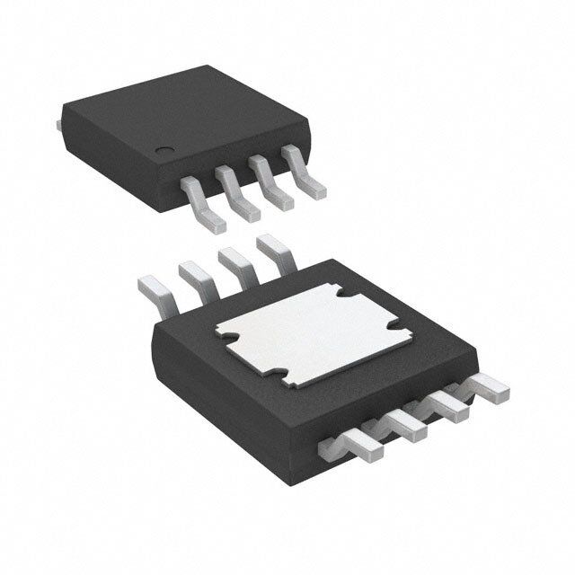
| 产品图片 |
|
| rohs | 符合RoHS无铅 / 符合限制有害物质指令(RoHS)规范要求 |
| 产品系列 | 电源管理 IC,线性稳压器,Analog Devices ADP124ARHZ-1.8-R7- |
| 数据手册 | |
| 产品型号 | ADP124ARHZ-1.8-R7 |
| 产品目录页面 | |
| 产品种类 | |
| 供应商器件封装 | 8-MSOP-EP |
| 其它名称 | ADP124ARHZ-1.8-R7CT |
| 包装 | 剪切带 (CT) |
| 商标 | Analog Devices |
| 安装类型 | 表面贴装 |
| 安装风格 | SMD/SMT |
| 封装 | Reel |
| 封装/外壳 | 8-TSSOP,8-MSOP(0.118",3.00mm 宽)裸焊盘 |
| 封装/箱体 | MSOP-8 |
| 工作温度 | -40°C ~ 85°C |
| 工厂包装数量 | 1000 |
| 最大工作温度 | + 125 C |
| 最大输入电压 | 5.5 V |
| 最小工作温度 | - 40 C |
| 最小输入电压 | 2.3 V |
| 标准包装 | 1 |
| 电压-跌落(典型值) | - |
| 电压-输入 | 2.3 V ~ 5.5 V |
| 电压-输出 | 1.8V |
| 电流-输出 | 500mA |
| 电流-限制(最小值) | 550mA |
| 稳压器拓扑 | 正,固定式 |
| 稳压器数 | 1 |
| 系列 | ADP124 |
| 视频文件 | http://www.digikey.cn/classic/video.aspx?PlayerID=1364138032001&width=640&height=505&videoID=2245193149001 |
| 输出电流 | 500 mA |


- 商务部:美国ITC正式对集成电路等产品启动337调查
- 曝三星4nm工艺存在良率问题 高通将骁龙8 Gen1或转产台积电
- 太阳诱电将投资9.5亿元在常州建新厂生产MLCC 预计2023年完工
- 英特尔发布欧洲新工厂建设计划 深化IDM 2.0 战略
- 台积电先进制程称霸业界 有大客户加持明年业绩稳了
- 达到5530亿美元!SIA预计今年全球半导体销售额将创下新高
- 英特尔拟将自动驾驶子公司Mobileye上市 估值或超500亿美元
- 三星加码芯片和SET,合并消费电子和移动部门,撤换高东真等 CEO
- 三星电子宣布重大人事变动 还合并消费电子和移动部门
- 海关总署:前11个月进口集成电路产品价值2.52万亿元 增长14.8%


PDF Datasheet 数据手册内容提取
5.5 V Input, 500 mA, Low Quiescent Current, CMOS Linear Regulators Data Sheet ADP124/ADP125 FEATURES TYPICAL APPLICATION CIRCUITS Input voltage supply range: 2.3 V to 5.5 V 500 mA maximum output current VOUT = 3.3V 1 VOUT VIN 8 VIN = 5.5V ADP124 Fixed and adjustable output voltage versions C2 2 VOUT VIN 7 C1 1% initial accuracy VOUT Up to 31 fixed-output voltage options available 3 SENSE NC 6 Adfjruosmta 1b.l7e5-o Vu ttop u3t.3 v Vol tage range from 0.8 V to 5.0 V 4 GND EN 5 ONOFF 08476-001 Very low dropout voltage: 130 mV Figure 1. ADP124 with Fixed Output Voltage Low quiescent current: 45 µA Low shutdown current: <1 µA VOUT = 3.3V Excellent PSRR performance: 60 dB at 100 kHz 1 VOUT VIN 8 VIN = 5.5V Excellent load/line transient response ADP125 Optimized for small 1.0 μF ceramic capacitors C2 R1 2 VOUT VIN 7 C1 Current limit and thermal overload protection 3 ADJ NC 6 Logic controlled enable R2 ON Compact 8-lead exposed paddle MSOP and LFCSP packages 4 GND EN 5 OFF 08476-002 APPLICATIONS Figure 2. ADP125 with Adjustable Output Voltage Digital camera and audio devices Portable and battery-powered equipment Automatic meter reading (AMR) meters GPS and location management units Medical instrumentation Point of load power GENERAL DESCRIPTION The ADP124/ADP125 are low quiescent current, low dropout The ADP124/ADP125 are specifically designed for stable linear regulators. They are designed to operate from an input operation with tiny 1 µF ceramic input and output capacitors to voltage between 2.3 V and 5.5 V and to provide up to 500 mA meet the requirements of high performance, space constrained of output current. The low 130 mV dropout voltage at a 500 mA applications. load improves efficiency and allows operation over a wide input The ADP124/ADP125 have an internal soft start that gives a voltage range. constant start-up time of 350 µs. Short-circuit protection and The low 210 μA of quiescent current with a 500 mA load makes the thermal overload protection circuits prevent damage in adverse ADP124/ADP125 ideal for battery-operated portable equipment. conditions. The ADP124/ADP125 are available in 8-lead exposed paddle MSOP and LFCSP packages. When compared The ADP124 is capable of 31 fixed-output voltages from 1.75 V with the standard MSOP and LFCSP packages, the exposed to 3.3 V. The ADP125 is the adjustable version of the device and paddle MSOP and LFCSP packages have lower thermal resistance allows the output voltage to be set between 0.8 V and 5.0 V by (θ ). The lower thermal resistance package allows the ADP124/ an external voltage divider. JA ADP125 to meet the needs of a variety of portable applications while minimizing the rise in junction temperature. Rev. D Document Feedback Information furnished by Analog Devices is believed to be accurate and reliable. However, no responsibility is assumed by Analog Devices for its use, nor for any infringements of patents or other One Technology Way, P.O. Box 9106, Norwood, MA 02062-9106, U.S.A. rights of third parties that may result from its use. Specifications subject to change without notice. No license is granted by implication or otherwise under any patent or patent rights of Analog Devices. Tel: 781.329.4700 ©2009–2014 Analog Devices, Inc. All rights reserved. Trademarks and registered trademarks are the property of their respective owners. Technical Support www.analog.com
ADP124/ADP125 Data Sheet TABLE OF CONTENTS Features .............................................................................................. 1 Typical Performance Characteristics ..............................................7 Applications ....................................................................................... 1 Theory of Operation ...................................................................... 11 Typical Application Circuits ............................................................ 1 Applications Information .............................................................. 12 General Description ......................................................................... 1 Capacitor Selection .................................................................... 12 Revision History ............................................................................... 2 Undervoltage Lockout ............................................................... 13 Specifications ..................................................................................... 3 Enable Feature ............................................................................ 13 Recommended Capacitor Specifications ................................... 4 Current Limit and Thermal Overload Protection ................. 14 Absolute Maximum Ratings ............................................................ 5 Thermal Considerations ............................................................ 14 Thermal Data ................................................................................ 5 Junction Temperature Calculations ......................................... 15 Thermal Resistance ...................................................................... 5 Printed Circuit Board Layout Considerations........................ 16 ESD Caution .................................................................................. 5 Outline Dimensions ....................................................................... 17 Pin Configurations and Function Descriptions ........................... 6 Ordering Guide .......................................................................... 18 REVISION HISTORY 12/14—Rev. C to Rev. D Updated Figure 46; Outline Dimensions ..................................... 17 Changes to Ordering Guide .......................................................... 18 6/12—Rev. B to Rev. C Changes to Table 3 ............................................................................ 5 Updated Outline Dimensions ....................................................... 17 4/12—Rev. A to Rev. B Updated Outline Dimensions ....................................................... 17 Changes to Ordering Guide .......................................................... 18 9/10—Rev. 0 to Rev. A Added 8-Lead LFCSP Package ..................................... Throughout Added Figure 4 and Figure 6 (Renumbered Sequentially) ......... 6 Changes to Thermal Conditions Section and Table 6 ............... 14 Added Table 7 .................................................................................. 14 Changes to Junction Temperature Calculations Section ........... 15 Added Figure 44 .............................................................................. 16 Updated Outline Dimensions ....................................................... 17 Changes to Ordering Guide .......................................................... 18 12/09—Revision 0: Initial Version Rev. D | Page 2 of 20
Data Sheet ADP124/ADP125 SPECIFICATIONS Unless otherwise noted, V = (V + 0.5 V) or 2.3 V, whichever is greater; ADJ connected to VOUT; I = 10 mA; C = 1.0 µF; IN OUT OUT IN C = 1.0 µF; T = 25°C. OUT A Table 1. Parameter Symbol Test Conditions Min Typ Max Unit INPUT VOLTAGE RANGE V 2.3 5.5 V IN OPERATING SUPPLY CURRENT1 I I = 0 µA 45 µA GND OUT I = 0 µA, T = −40°C to +125°C 105 µA OUT J I = 1 mA 60 µA OUT I = 1 mA, T = −40°C to +125°C 120 µA OUT J I = 250 mA 160 µA OUT I = 250 mA, T = −40°C to +125°C 210 µA OUT J I = 500 mA 210 µA OUT I = 500 mA, T = −40°C to +125°C 280 µA OUT J SHUTDOWN CURRENT I EN = GND 0.1 µA SD EN = GND, T = −40°C to +125°C 1 µA J OUTPUT VOLTAGE ACCURACY2 V OUT Fixed Output I = 10 mA −1 +1 % OUT 100 µA < I < 500 mA, V = (V + 0.5 V) to 5.5 V, −2 +1.5 % OUT IN OUT T = −40°C to +125°C J Adjustable Output I = 10 mA 0.495 0.500 0.505 V OUT 100 µA < I < 500 mA, V = 2.3 V to 5.5 V, 0.485 0.500 0.515 V OUT IN T = −40°C to +125°C J LINE REGULATION ∆V /∆V V = V = 2.3 V to 5.5 V, T = −40°C to +125°C −0.05 +0.05 %/V OUT IN IN IN J LOAD REGULATION3 ∆VOUT/∆IOUT IOUT = 1 mA to 500 mA 0.0005 %/mA I = 1 mA to 500 mA, T = −40°C to +125°C 0.001 %/mA OUT J ADJ INPUT BIAS CURRENT ADJ 2.3 V ≤ V ≤ 5.5 V, ADJ connected to VOUT 15 nA I-BIAS IN DROPOUT VOLTAGE4 VDROPOUT I = 10 mA, V > 2.3 V 3 mV OUT OUT I = 10 mA, T = −40°C to +125°C 5 mV OUT J I = 250 mA, V > 2.3 V 65 mV OUT OUT I = 250 mA, T = −40°C to +125°C 120 mV OUT J I = 500 mA, V > 2.3V 130 mV OUT OUT I = 500 mA, T = −40°C to +125°C 230 mV OUT J START-UP TIME5 tSTART-UP VOUT = 3.0 V 350 µs CURRENT LIMIT THRESHOLD6 I 550 750 1000 mA LIMIT THERMAL SHUTDOWN Thermal Shutdown Threshold TSSD TJ rising 150 °C Thermal Shutdown Hysteresis TSSD-HYS 15 °C EN INPUT EN Input Logic High V 2.3 V ≤ V ≤ 5.5 V 1.2 V IH IN EN Input Logic Low V 2.3 V ≤ V ≤ 5.5 V 0.4 V IL IN EN Input Leakage Current V EN = VIN or GND 0.1 µA I-LEAKAGE EN = VIN or GND, T = −40°C to +125°C 1 µA J UNDERVOLTAGE LOCKOUT UVLO Input Voltage Rising UVLO T = −40°C to +125°C 2.1 V RISE J Input Voltage Falling UVLO T = −40°C to +125°C 1.5 V FALL J Hysteresis UVLO T = 25°C 125 mV HYS A Rev. D | Page 3 of 20
ADP124/ADP125 Data Sheet Parameter Symbol Test Conditions Min Typ Max Unit OUTPUT NOISE OUT 10 Hz to 100 kHz, V = 5.5 V, V = 1.2 V 25 µV rms NOISE IN OUT 10 Hz to 100 kHz, V = 5.5 V, V = 1.8 V 35 µV rms IN OUT 10 Hz to 100 kHz, V = 5.5 V, V = 2.5 V 45 µV rms IN OUT 10 Hz to 100 kHz, V = 5.5 V, V = 3.3 V 55 µV rms IN OUT 10 Hz to 100 kHz, V = 5.5 V, V = 4.2V 65 µV rms IN OUT POWER SUPPLY REJECTION RATIO PSRR 10 kHz to 100 kHz, V = 1.8 V, 2.5 V, 3.3 V 60 dB OUT (V = V +1V) IN OUT 1 The current from the external resistor divider network in the case of adjustable voltage output (as with the ADP125) should be subtracted from the ground current measured. 2 Accuracy when VOUT is connected directly to ADJ. When VOUT voltage is set by external feedback resistors, absolute accuracy in adjust mode depends on the tolerances of the resistors used. 3 Based on an endpoint calculation using 1 mA and 500 mA loads. 4 Dropout voltage is defined as the input-to-output voltage differential when the input voltage is set to the nominal output voltage. This applies only for output voltages greater than 2.3 V. 5 Start-up time is defined as the time between the rising edge of EN to VOUT being at 90% of its nominal value. 6 Current limit threshold is defined as the current at which the output voltage drops to 90% of the specified typical value. For example, the current limit for a 3.3 V output voltage is defined as the current that causes the output voltage to drop to 90% of 3.3 V, or 2.97 V. RECOMMENDED CAPACITOR SPECIFICATIONS Table 2. Parameter Symbol Test Conditions Min Typ Max Unit Minimum Input and Output CAP T = −40°C to +125°C 0.70 µF MIN A Capacitance1 Capacitor ESR R T = −40°C to +125°C 0.001 1 Ω ESR A 1 The minimum input and output capacitance should be greater than 0.70 µF over the full range of operating conditions. The full range of operating conditions in the application must be considered during device selection to ensure that the minimum capacitance specification is met. X7R and X5R type capacitors are recommended; Y5V and Z5U capacitors are not recommended for use with this LDO. Rev. D | Page 4 of 20
Data Sheet ADP124/ADP125 ABSOLUTE MAXIMUM RATINGS application and board layout. In applications in which high maxi- Table 3. mum power dissipation exists, close attention to thermal board Parameter Rating design is required. The value of θ may vary, depending on PCB VIN to GND −0.3 V to +6.5 V JA material, layout, and environmental conditions. The specified ADJ to GND −0.3 V to +6.5 V values of θ are based on a 4-layer, 4 inch × 3 inch circuit board. EN to GND −0.3 V to +6.5 V JA Refer to JESD 51-7 for detailed information on the board VOUT to GND −0.3 V to VIN construction. Storage Temperature Range −65°C to +150°C Operating Ambient Temperature Range −40°C to +85°C ΨJB is the junction-to-board thermal characterization parameter Operating Junction Temperature Range −40°C to +125°C and is measured in °C/W. The ΨJB of the package is based on Soldering Conditions JEDEC J-STD-020 modeling and calculation using a 4-layer board. The Guidelines for Reporting and Using Package Thermal Information: JESD51-12 states that thermal characterization parameters are not the same Stresses above those listed under Absolute Maximum Ratings as thermal resistances. Ψ measures the component power flowing may cause permanent damage to the device. This is a stress JB through multiple thermal paths rather than a single path as in rating only; functional operation of the device at these or any thermal resistance, θ . Therefore, Ψ thermal paths include other conditions above those indicated in the operational JB JB convection from the top of the package as well as radiation from section of this specification is not implied. Exposure to absolute the package—factors that make Ψ more useful in real-world maximum rating conditions for extended periods may affect JB applications. Maximum junction temperature (T) is calculated device reliability. J from the board temperature (T ) and power dissipation (P ) B D THERMAL DATA using the formula Absolute maximum ratings apply individually only, not in T = T + (P × Ψ ) J B D JB combination. The ADP124/ADP125 can be damaged when the Refer to JESD51-8 and JESD51-12 for more detailed information junction temperature limits are exceeded. Monitoring ambient about Ψ . temperature does not guarantee that T will remain within the JB J specified temperature limits. In applications with high power THERMAL RESISTANCE dissipation and poor thermal resistance, the maximum ambient θ and Ψ are specified for the worst-case conditions, that is, a JA JB temperature may have to be limited. device soldered in a circuit board for surface-mount packages. In applications with moderate power dissipation and low PCB Table 4. Thermal Resistance thermal resistance, the maximum ambient temperature can Package Type θ Ψ Unit exceed the maximum limit as long as the junction temperature JA JB 8-Lead MSOP 102.8 31.8 °C/W is within specification limits. The junction temperature (T) of J 8-Lead LFCSP 68.9 44.1 °C/W the device is dependent on the ambient temperature (T ), the A power dissipation of the device (P ), and the junction-to-ambient D thermal resistance of the package (θ ). ESD CAUTION JA Maximum junction temperature (T) is calculated from the J ambient temperature (T ) and power dissipation (P ) using the A D formula T = T + (P × θ ) J A D JA The junction-to-ambient thermal resistance (θ ) of the package JA is based on modeling and calculation using a 4-layer board. The junction-to-ambient thermal resistance is highly dependent on the Rev. D | Page 5 of 20
ADP124/ADP125 Data Sheet PIN CONFIGURATIONS AND FUNCTION DESCRIPTIONS VOUT 1 8 VIN VOUT 1 8 VIN VOUT 2 ADP124 7 VIN VOUT 2 ADP125 7 VIN TOP VIEW TOP VIEW VOUT SEGNNSDE 34 (Not to Scale) 65 NENC 08476-003 GANDDJ 34 (Not to Scale) 65 NENC 08476-004 NOTES NOTES 1. NC = NO CONNECT. 1. NC = NO CONNECT. 2. THE EXPOSEDPAD MUST BE CONNECTEDTO GROUND. 2. THE EXPOSEDPAD MUST BE CONNECTEDTO GROUND. Figure 3. ADP124 Fixed Output MSOP Pin Configuration Figure 5. ADP125 Adjustable Output MSOP Pin Configuration VOUT 1 8 VIN VOUT 1 8 VIN VOUT 2 ADP124 7 VIN VOUT 2 ADP125 7 VIN TOP VIEW TOP VIEW VOUT SENSE 3 (Not to Scale) 6 NC ADJ 3 (Not to Scale) 6 NC GND 4 5 EN 08476-105 GND 4 5 EN 08476-106 NOTES NOTES 1. NC = NO CONNECT. 1. NC = NO CONNECT. 2. THE EXPOSEDPAD MUST BE CONNECTEDTO GROUND. 2. THE EXPOSEDPAD MUST BE CONNECTEDTO GROUND. Figure 4. ADP124 Fixed Output LFCSP Pin Configuration Figure 6. ADP125 Adjustable Output LFCSP Pin Configuration Table 5. Pin Function Descriptions Mnemonic Pin No. ADP124 ADP125 Description 1 VOUT VOUT Regulated Output Voltage. Bypass VOUT to GND with a 1 μF or greater capacitor. 2 VOUT VOUT Regulated Output Voltage. Bypass VOUT to GND with a 1 μF or greater capacitor. 3 VOUT SENSE N/A Feedback Node for the Error Amplifier. Connect to VOUT. N/A ADJ Feedback Node for the Error Amplifier. Connect the midpoint of an external divider from VOUT to GND to this pin to set the output voltage. 4 GND GND Ground. 5 EN EN Enable Input. Drive EN high to turn on the regulator; drive EN low to turn off the regulator. For automatic startup, connect EN to VIN. 6 NC NC No Connect. This pin is not connected internally. 7 VIN VIN Regulator Input Supply. Bypass VIN to GND with a 1 μF or greater capacitor. 8 VIN VIN Regulator Input Supply. Bypass VIN to GND with a 1 μF or greater capacitor. EPAD EPAD The exposed pad must be connected to ground. Rev. D | Page 6 of 20
Data Sheet ADP124/ADP125 TYPICAL PERFORMANCE CHARACTERISTICS V = 3.8 V, V = 3.3V, I = 10 mA, C = 1.0 µF, C = 1.0 µF, T = 25°C, unless otherwise noted. IN OUT OUT IN OUT A 3.310 300 3.305 250 3.300 A) IOUT = 500mA µ V) 3.295 RENT (200 V (OUT 33..228950 IIIIOOOOUUUUTTTT ==== 11110m000m0AµmAAA OUND CUR150 IOUT = 300mA 3.280 IIOOUUTT == 350000mmAA GR IOUT = 100mA IOUT = 100µA 100 IOUT = 1mA 3.275 IOUT = 10mA 3.270 –40 JU–N5CTION TE+M2P5ERATURE+ 8(5°C) +125 08476-005 50 –40 JU–N5CTION TE+M2P5ERATURE+ 8(°5C) +125 08476-008 Figure 7. Output Voltage vs. Junction Temperature Figure 10. Ground Current vs. Junction Temperature 3.309 250 3.308 200 A) µ 3.307 T ( V) REN 150 (OUT3.306 CUR V D N 100 U 3.305 O R G 50 3.304 3.303 0 0.1 1 IOUT10(mA) 100 1000 08476-006 0.1 1 ILOA1D0 (mA) 100 1000 08476-009 Figure 8. Output Voltage vs. Load Current Figure 11. Ground Current vs. Load Current 3.310 250 IOUT = 500mA 3.308 230 3.306 210 3.304 T (µA) 190 IOUT = 300mA V) 3.302 REN 170 V (OUT3.300 IIOOUUTT == 110m0AµA ND CUR 113500 IOUT = 100mA 3.298 IOUT = 10mA OU 3.296 IIIOOOUUUTTT === 135000000mmmAAA GR 19100 IOUT = 10mA IOUT = 1mA IOUT = 100µA 3.294 70 3.292 50 3.50 4.00 V4IN.5 (0V) 5.00 5.50 08476-007 3.50 4.00 V4IN.5 (0V) 5.00 5.50 08476-010 Figure 9. Output Voltage vs. Input Voltage Figure 12. Ground Current vs. Input Voltage Rev. D | Page 7 of 20
ADP124/ADP125 Data Sheet 0.7 3.35 0.6 3.30 IOUT = 10mA IOUT = 100mA NT (µA) 0.5 VVIINN == 55..4500 3.25 IIOOUUTT == 350000mmAA WN CURRE 00..34 VVVVIIIINNNN ==== 4455....24020000 V (V)OUT33..1250 DO VIN = 3.80 3.10 T U 0.2 H S 3.05 0.1 3.00 0–50 –25 0 TE2M5PERAT5U0RE (°C7)5 100 125 08476-011 2.953.00 3.10 3.20 V3IN.3 (0V) 3.40 3.50 3.60 08476-014 Figure 13. Shutdown Current vs. Temperature at Various Input Voltages Figure 16. Output Voltage vs. Input Voltage (in Dropout) 120 –10 –20 100 IOUT = 100µA –30 IOUT = 1mA IOUT = 10mA V) 80 –40 IOUT = 100mA m B) IOUT = 300mA OUT ( 60 RR (d –50 IOUT = 500mA OP PS –60 R D 40 –70 –80 20 VIN = VOUT +1V –90 VRIPPLE = 50mV CIN = COUT = 1µF 0 1 10 IOUT (mA) 100 1000 08476-012 –10010 100 1kFREQU1E0NkCY (Hz)100k 1M 10M 08476-015 Figure 14. Dropout Voltage vs. Load Current Figure 17. Power Supply Rejection Ratio vs. Frequency, VOUT = 2.8 V, VIN = 3.8 V 450 –10 400 –20 350 –30 IIOOUUTT == 11m00AµA IOUT = 10mA 300 –40 IOUT = 100mA I (µA)GND220500 IIIIOOOOUUUUTTTT ==== 11350000000mmmmAAAA PSRR (dB) ––6500 IIOOUUTT == 350000mmAA 150 –70 100 –80 VIN = VOUT +1V 50 –90 VRIPPLE = 50mV CIN = COUT = 1µF 0 –100 3.00 3.10 3.20 3.30VIN (V3).40 3.50 3.60 3.70 08476-013 10 100 1kFREQU1E0NkCY (Hz)100k 1M 10M 08476-016 Figure 15. Ground Current vs. Input Voltage (in Dropout) Figure 18. Power Supply Rejection Ratio vs. Frequency, VOUT = 3.3 V, VIN = 4.3 V Rev. D | Page 8 of 20
Data Sheet ADP124/ADP125 –10 5 –20 –30 IIOOUUTT == 110m0AµA 4 VOUT = 4.2V IOUT = 10mA R (dB) ––5400 IIIOOOUUUTTT === 135000000mmmAAA (µv/√Hz) 3 VOUT = 3.3V R E PS –60 OIS N 2 –70 –80 VIN = VOUT + 1V 1 VOUT = 2.8V ––1900010 VCRINIP =P1 L0CE0O =U T5 0=m 1Vµ1Fk 10k 100k 1M 10M08476-017 010 100 1k 10k 100k08476-020 FREQUENCY (Hz) FREQUENCY (Hz) Figure 19. Power Supply Rejection Ratio vs. Frequency, VOUT = 4.2 V, VIN = 5.2 V Figure 22. Output Noise Spectrum, VIN = 5 V –10 70 –20 VVOOUUTT == 23..83VV,, IIOOUUTT == 1100mmAA 65 VOUT = 4.2V VOUT = 4.2V, IOUT = 10mA 60 –30 VVOOUUTT == 23..83VV,, IIOOUUTT == 550000mmAA 55 VOUT = 3.3V RR (dB) ––5400 VOUT = 4.2V, IOUT = 500mA OISE (µV) 4550 VOUT = 2.8V PS –60 MS N 40 –70 R 35 –80 30 VIN = VOUT + 1V ––19000 VCRINIP =P LCEO =U T5 0=m 1VµF 08476-018 2205 08476-021 10 100 1k 10k 100k 1M 10M 0.001 0.01 0.1 1 10 100 1k FREQUENCY (Hz) ILOAD (mA) Figure 20. Power Supply Rejection Ratio vs. Frequency, Figure 23. Output Noise vs. Load Current and Output Voltage, VIN = 5 V Various Output Voltages and Load Currents –10 VIN = 3.1V, IOUT = 10mA IOUT –20 VIN = 3.3V, IOUT = 10mA VIN = 3.8V, IOUT = 10mA 1mA TO 500mA LOAD STEP –30 VIN = 4.8V, IOUT = 10mA 1 –40 dB) –50 R ( PSR –60 VOUT 2 –70 –80 VIN = 3.1V, IOUT = 500mA VIN = 3.3V, IOUT = 500mA VIN = 4V –1–0900 VVIINN == 34..88VV,, IIOOUUTT == 550000mmAA 08476-019 VOUT = 3.3V 08476-022 10 100 1k 10k 100k 1M 10M CH1 500mA ΩBW CH2 50.0mV BW M40.0µs A CH1 200mA FREQUENCY (Hz) T 9.800% Figure 21. Power Supply Rejection Ratio vs. Headroom Voltage (VIN − VOUT), Figure 24. Load Transient Response, COUT = 1 μF VOUT = 2.8 V Rev. D | Page 9 of 20
ADP124/ADP125 Data Sheet IOUT 1mA TO 500mA LOAD STEP VIN 1 4V TO 4.5V VOLTAGE STEP VOUT 2 2 VOUT 1 VVIONU =T 4=V 3.3V 08476-023 08476-025 CH1 500mA ΩBW CH2 50.0mV BW M40.0µs A CH1 200mA CH1 1.00VBW CH2 2.00mV BW M10.0µs A CH3 200mA T 9.800% T 9.800% Figure 25. Load Transient Response, COUT = 4.7 μF Figure 27. Line Transient Response, Load Current = 500 mA VIN 4V TO 4.5V VOLTAGE STEP VOUT 2 1 08476-024 CH1 1.00VBW CH2 2.00mV BW M10.0µs A CH3 2.36V T 9.600% Figure 26. Line Transient Response, Load Current = 1 mA Rev. D | Page 10 of 20
Data Sheet ADP124/ADP125 THEORY OF OPERATION The ADP124/ADP125 are low quiescent current, low dropout The ADP124/ADP125 use the EN pin to enable and disable the linear regulators that operate from 2.3 V to 5.5 V and can provide VOUT pin under normal operating conditions. When EN is high, up to 500 mA of output current. Drawing a low 210 µA of quies- VOUT turns on; when EN is low, VOUT turns off. For automatic cent current (typical) at full load makes the ADP124/ADP125 startup, EN can be tied to VIN. ideal for battery-operated portable equipment. Shutdown current consumption is typically 100 nA. ADP124 VIN VOUT Optimized for use with small 1 µF ceramic capacitors, the VOUT SENSE ADP124/ADP125 provide excellent transient performance. SHORT CIRCUIT, UVLO,AND Internally, the ADP124/ADP125 consist of a reference, an error THERMAL R1 GND PROTECT amplifier, a feedback voltage divider, and a PMOS pass transistor. Output current is delivered via the PMOS pass device, which is controlled by the error amplifier. The error amplifier compares the reference voltage with the feedback voltage from the output EN SHUTDOWN 0.5V REFERENCE R2 and amplifies the difference. If the feedback voltage is lower than the reference voltage, the gate of the PMOS device is pulled lower, aIfl ltohwe ifnege dmboarcek cvuorlrtaegnet tiso hpiagshse arn tdh ainnc trheea srienfegr tehnec eo uvtoplutatg veo, ltthaeg e. N1 . O RTTH1EEASNADD PR1224A ROEN LINYT.ERNAL RESISTORS,AVAILABLE ON 08476-121 gate of the PMOS device is pulled higher, allowing less current Figure 28. ADP124 Internal Block Diagram (Fixed Output) to pass and decreasing the output voltage. The adjustable ADP125 has an output voltage range of 0.8 V to ADP125 5.0 V. The output voltage is set by the ratio of two external resistors, VIN VOUT as shown in Figure 2. The device servos the output to maintain the voltage at the ADJ pin at 0.5 V referenced to ground. The SHORT CIRCUIT, current in R1 is then equal to 0.5 V/R2 and the current in R1 is UVLO,AND THERMAL the current in R2 plus the ADJ pin bias current. The ADJ pin GND PROTECT bias current, 15 nA at 25°C, flows through R1 into the ADJ pin. The output voltage can be calculated using the equation: ADJ VOUT = 0.5 V(1 + R1/R2) + (ADJI-BIAS)(R1) EN SHUTDOWN 0.5V REFERENCE Tinh teh vea oluuetp ouft R v1o lsthagoeu lcda ubsee lde sbsy t hthaen A20D0J kpΩin tboi ams icnuimrreiznet .e Frroorr s 08476-122 example, when R1 and R2 each equal 200 kΩ, the output voltage Figure 29. ADP125 Internal Block Diagram (Adjustable Output) is 1.0 V. The output voltage error introduced by the ADJ pin bias current is 3 mV or 0.3%, assuming a typical ADJ pin bias current of 15 nA at 25°C. Note that in shutdown, the output is turned off and the divider current is 0. Rev. D | Page 11 of 20
ADP124/ADP125 Data Sheet APPLICATIONS INFORMATION CAPACITOR SELECTION Input Bypass Capacitor Output Capacitor Connecting a 1 µF capacitor from VIN to GND reduces the circuit sensitivity to the printed circuit board (PCB) layout, especially The ADP124/ADP125 are designed for operation with small, when a long input trace or high source impedance is encountered. space-saving ceramic capacitors, but these devices can function If greater than 1 µF of output capacitance is required, the input with most commonly used capacitors as long as care is taken to capacitor should be increased to match it. ensure an appropriate effective series resistance (ESR) value. The ESR of the output capacitor affects the stability of the LDO control Input and Output Capacitor Properties loop. A minimum of 0.70 µF capacitance with an ESR of 1 Ω or Any good quality ceramic capacitors can be used with the less is recommended to ensure stability of the ADP124/ADP125. ADP124/ADP125, as long as the capacitor meets the minimum The transient response to changes in load current is also affected by capacitance and maximum ESR requirements. Ceramic capacitors the output capacitance. Using a larger value of output capacitance are manufactured with a variety of dielectrics, each with different improves the transient response of the ADP124/ADP125 to behavior over temperature and applied voltage. Capacitors must dynamic changes in load current. Figure 30 and Figure 31 show have an adequate dielectric to ensure the minimum capacitance the transient responses for output capacitance values of 1 µF and over the necessary temperature range and dc bias conditions. 4.7 µF, respectively. Using an X5R or X7R dielectric with a voltage rating of 6.3 V or 10 V is recommended. However, using Y5V and Z5U dielectrics IOUT are not recommended for any LDO, due to their poor temperature 1mA TO 500mA LOAD STEP and dc bias characteristics. 1 Figure 32 depicts the capacitance vs. capacitor voltage bias charac- teristics of an 0402, 1 µF, 10 V X5R capacitor. The voltage stability of a capacitor is strongly influenced by the capacitor size and the voltage rating. In general, a capacitor in a larger package or of a 2 higher voltage rating exhibits better stability. The temperature VOUT variation of the X5R dielectric is about ±15% over the −40°C to +85°C temperature range and is not a function of package or VVIONU =T 4=V 3.3V 08476-028 voltage1 .r1a0ting. CH1 500mA ΩBW CH2 50.0mV BW M400ns A CH1 200mA T 13.20% 1.05 Figure 30. Output Transient Response, COUT = 1 µF 1.00 F) E (µ0.95 IOUT NC A0.90 T 1mA TO 500mA LOAD STEP CI A 1 AP0.85 C 0.80 2 00..7705 08476-030 0 1 2 3 4 5 6 7 VOUT BIAS VOLTAGE (V) Figure 32. Capacitance vs. Capacitor Voltage Bias Characteristics VVIONU =T 4=V 3.3V 08476-029 Eacqcuoautniotnin 1g cfoanr cbaep uacsietdo rt ov adreiatetiromni noev etrh tee wmopresrta-ctuasree , ccaopmacpitoannecnet, CH1 500mA ΩBW CH2 50.0mV BW M400ns A CH1 200mA T 13.60% tolerance, and voltage. Figure 31. Output Transient Response, COUT = 4.7 µF C = C × (1 − TEMPCO) × (1 − TOL) (1) EFF where: C is the effective capacitance at the operating voltage. EFF C is the rated capacitance value. TEMPCO is the worst-case capacitor temperature coefficient. TOL is the worst-case component tolerance. Rev. D | Page 12 of 20
Data Sheet ADP124/ADP125 In this example, the worst-case temperature coefficient (TEMPCO) The active and inactive thresholds of the EN pin are derived from over −40°C to +85°C is assumed to be 15% for an X5R dielectric. the VIN voltage. Therefore, these thresholds vary as the input The tolerance of the capacitor (TOL) is assumed to be 10%, and voltage changes. Figure 34 shows typical EN active and inactive C is 0.94 μF at 4.2 V from the graph in Figure 32. thresholds when the VIN voltage varies from 2.3 V to 5.5 V. Substituting these values in Equation 1 yields 1.05 C = 0.94 μF × (1 − 0.15) × (1 − 0.1) = 0.719 μF 1.00 EFF Therefore, the capacitor chosen in this example meets the S (V)0.95 minimum capacitance requirement of the LDO over tem- LD0.90 RISING O perature and tolerance at the chosen output voltage. ESH0.85 R To guarantee the performance of the ADP124/ADP125, it is N) T0.80 iomn ptherea btievhea tvhiaotr tohfe t ehfef eccatps aocfi tdocr sb iaarse, etevmalupaetreadtu froer, eaancdh t oapleprlaincacteiso n. BLE (E0.75 FALLING A UNDERVOLTAGE LOCKOUT EN0.70 Tcihrceu AitD thPa1t2 d4/iAsaDblPe1s 2a5ll h inavpeu atsn a inndte rthnea lo uuntpduertv wohlteange t hloec kinopuut t 00..6605 08476-032 2.2 2.7 3.2 3.7 4.2 4.7 5.2 voltage is less than approximately 2 V. This ensures that the VIN (V) ADP124/ADP125 inputs and the output behave in a predictable Figure 34. Typical EN Pin Thresholds vs. Input Voltage manner during power-up. The ADP124/ADP125 use an internal soft start to limit the ENABLE FEATURE inrush current when the output is enabled. The start-up time The ADP124/ADP125 uses the EN pin to enable and disable the for the 2.8 V option is approximately 350 µs from the time the VOUT pin under normal operating conditions. As shown in EN active threshold is crossed to when the output reaches 90% Figure 33, when a rising voltage on EN crosses the active threshold, of its final value. As shown in Figure 35, the start-up time is VOUT turns on. Conversely, when a falling voltage on EN crosses dependent on the output voltage setting and increases slightly the inactive threshold, VOUT turns off. as the output voltage increases. 3.5 3.0 VIN = 5V VOUT = 4.2V 2.5 VOUT = 3.3V 2.0 OUT VOUT = 2.8V V 1.5 1.0 1 2 0.5 00 0.2 0.4 0.6 0.8 1.0 1.2 1.4 1.608476-230 08476-033 VEN CH1 1.00V CH2 1.00VBW MT 1 0 0 µ 2s96.800µsA CH1 2.00V Figure 33. Typical EN Pin Operation Figure 35. Typical Start-Up Time As shown in Figure 33, the EN pin has built-in hysteresis. This prevents on/off oscillations that may occur due to noise on the EN pin as it passes through the threshold points. Rev. D | Page 13 of 20
ADP124/ADP125 Data Sheet CURRENT LIMIT AND THERMAL OVERLOAD Table 6. Typical θ Values for Specified PCB Copper Sizes JA PROTECTION θ (°C/W) JA Copper The ADP124/ADP125 are protected from damage due to excessive Size (mm2) MSOP LFCSP power dissipation by current and thermal overload protection 25 108.6 177.8 circuits. The ADP124/ADP125 are designed to limit the current 100 75.5 138.2 when the output load reaches 750 mA (typical). When the output 500 42.5 79.8 load exceeds 750 mA, the output voltage is reduced to maintain 1000 34.7 67.8 a constant current limit. 6400 26.1 53.5 Thermal overload protection is included, which limits the junction temperature to a maximum of 150°C typical. Under extreme con- Table 7. Typical Ψ Values JB ditions (that is, high ambient temperature and power dissipation), Ψ (°C/W) JB when the junction temperature starts to rise above 150°C, the MSOP LFCSP output is turned off, reducing output current to zero. When the 31.7 44.1 junction temperature cools to less than 135°C, the output is turned on again and the output current is restored to its nominal value. The junction temperature of the ADP124/ADP125 can be calculated from the following equation: Consider the case where a hard short from VOUT to GND occurs. At first, the ADP124/ADP125 limit the current so that only T = T + (P × θ ) (2) J A D JA 750 mA is conducted into the short. If self-heating causes the where: junction temperature to rise above 150°C, thermal shutdown T is the ambient temperature. A activates, turning off the output and reducing the output P is the power dissipation in the die, given by D current to zero. When the junction temperature cools to less P = [(V − V ) × I ] + (V × I ) (3) than 135°C, the output turns on and conducts 750 mA into the D IN OUT LOAD IN GND short, again causing the junction temperature to rise above where: 150°C. This thermal oscillation between 135°C and 150°C results I is the load current. LOAD in a current oscillation between 750 mA and 0 mA that I is the ground current. GND continues as long as the short remains at the output. V and V are input and output voltages, respectively. IN OUT Current and thermal limit protections are intended to protect the The power dissipation due to ground current is quite small and device from damage due to accidental overload conditions. For can be ignored. Therefore, the junction temperature equation reliable operation, the device power dissipation must be externally can be simplified as follows: limited so that the junction temperature does not exceed 125°C. T = T + {[(V − V ) × I ] × θ } (4) J A IN OUT LOAD JA THERMAL CONSIDERATIONS As shown in Equation 4, for a given ambient temperature, input- To guarantee reliable operation, the junction temperature of the to-output voltage differential, and continuous load current, there ADP124/ADP125 must not exceed 125°C. To ensure that the exists a minimum copper size requirement for the PCB to ensure junction temperature is less than this maximum value, the user that the junction temperature does not rise above 125°C. Figure 36 needs to be aware of the parameters that contribute to junction through Figure 41 show junction temperature calculations for temperature changes. These parameters include ambient tem- different ambient temperatures, load currents, V to V IN OUT perature, power dissipation in the power device, and thermal differentials, and areas of PCB copper. resistances between the junction and ambient air (θ ). The value JA In cases where the board temperature is known, the thermal of θ is dependent on the package assembly compounds used JA characterization parameter, Ψ , can be used to estimate the jun- JB and the amount of copper to which the GND pins of the package ction temperature rise. The maximum junction temperature (T) is J are soldered on the PCB. Table 6 shows typical θ values of the JA calculated from the board temperature (T) and power dissipation B 8-lead MSOP package for various PCB copper sizes. Table 7 (P ) using the formula D shows typical Ψ values of the 8-lead MSOP and 8-lead 3 mm × JB T = T + (P × Ψ ) (5) 3 mm LFCSP package. J B D JB Rev. D | Page 14 of 20
Data Sheet ADP124/ADP125 JUNCTION TEMPERATURE CALCULATIONS 145 140 135 130 125 E (°C)115 E (°C) 120 R R U105 U 110 T T A A ER 95 ER 100 MP 85 MP N TE 75 N TE 90 O O TI 65 TI 80 C C UN 55 6400 mm2 UN 70 6400 mm2 J 45 500 mm2 J 500 mm2 2355 2T5J MmAmX2 08476-034 5600 2T5J MmAmX2 08476-037 024680246802468024680 0 0.2 0.4 0.6 0.8 1.0 1.2 1.4 1.6 1.8 0.0.0.0.1.1.1.1.1.2.2.2.2.2.3.3.3.3.3.4. TOTAL POWER DISSIPATION (W) TOTAL POWER DISSIPATION (W) Figure 36. Junction Temperature vs. Power Dissipation and copper area, Figure 39. Junction Temperature vs. Power Dissipation and copper area, MSOP, TA = 25°C LFCSP, TA = 50°C 145 140 135 120 125 C) C) E (°115 E (°100 R R U105 U T T A A R 95 R 80 E E MP 85 MP E E N T 75 N T 60 TIO 65 TIO TB = 25°C JUNC 23455555 652T405J 00 Mm0 m AmmmX2m22 08476-035 JUNC 24000 TTTTBBBJ M=== A568055X°°°CCC 08476-038 0 0.2 0.4 0.6 0.8 1.0 1.2 1.4 1.6 1.8 2.0 0 0.25 0.50 0.75 1.00 1.25 1.50 1.75 2.00 2.25 2.50 TOTAL POWER DISSIPATION (W) TOTAL POWER DISSIPATION (W) Figure 37. Junction Temperature vs. Power Dissipation and copper area, Figure 40. Junction Temperature vs. Power Dissipation, MSOP package LFCSP, TA = 25°C at various Board Temperatures 140 140 130 120 E (°C) 120 E (°C)100 R R U 110 U AT AT ER 100 ER 80 P P M M TE 90 TE 60 N N JUNCTIO 56780000 652T405J 00 Mm0 m AmmmX2m22 08476-036 JUNCTIO 24000 TTTTTBBBBJ M==== A25685055X°°°°CCCC 08476-039 0 0.2 0.4 0.6 0.8 1.0 1.2 1.4 1.6 1.8 2.0 2.2 2.4 2.6 2.8 3.0 0 0.5 1.0 1.5 2.0 2.5 3.0 3.5 4.0 4.5 TOTAL POWER DISSIPATION (W) TOTAL POWER DISSIPATION (W) Figure 38. Junction Temperature vs. Power Dissipation and copper area, Figure 41. Junction Temperature vs. Power Dissipation, LFCSP package MSOP, TA = 50°C at various Board Temperatures Rev. D | Page 15 of 20
ADP124/ADP125 Data Sheet PRINTED CIRCUIT BOARD LAYOUT CONSIDERATIONS Heat dissipation from the package can be improved by increasing the amount of copper attached to the pins of the ADP124/ ADP125. However, as shown in Table 6, a point of diminishing returns eventually is reached, beyond which an increase in the copper size does not yield significant heat dissipation benefits. The input capacitor should be placed as close as possible to the VIN and GND pins, and the output capacitor should be placed as close as possible to the VOUT and GND pins. Use of 0402 or 0603 size capacitors and resistors achieves the smallest possible footprint solution on boards where the area is limited. 08476-042 Figure 43. Example ADP125 MSOP PCB Layout 08476-041 Figure 42. Example ADP124 MSOP PCB Layout 08476-045 Figure 44. Example ADP124/ADP125 LFCSP PCB Layout Rev. D | Page 16 of 20
Data Sheet ADP124/ADP125 OUTLINE DIMENSIONS 3.10 3.00 1.825 2.90 1.725 1.625 3.10 8 5 5.05 1.760 32..0900 44..9705 EXPPOASDED 11..656600 1 4 FOR PROPER CONNECTION OF THE EXPOSED PAD, REFER TO THE PIN CONFIGURATION AND 0.65 TOP VIEW BOTTOM VIEW FUNCTION DESCRIPTIONS BSC 1.95 BSC SECTION OF THIS DATA SHEET. 0.94 0.86 SIDE VIEW 1M.1A0X 0.25P GLAAGNEE 0.23 0.78 0.08 0.13 0.40 6° END VIEW MAX 0.33 0° 0.70 0.95 COPLANARITY 0.25 0.55 REF 0.10 0.40 PKG-3371 COMPLIANT TO JEDEC STANDARDS MO-187-AA-T 06-04-2013-A Figure 45. 8-Lead Mini Small Outline Package with Exposed Pad [MINI_SO_EP] (RH-8-1) Dimensions shown in millimeters 1.70 1.60 2.10 1.50 2.00 SQ 1.90 0.50 BSC 5 8 0.15 REF PIN 1 INDEX EXPOSED 1.10 AREA PAD 1.00 0.425 0.90 0.350 0.275 4 1 PIN 1 TOP VIEW BOTTOM VIEW INDICATOR (R 0.15) 0.60 FOR PROPER CONNECTION OF 0.55 0.05 MAX THE EXPOSED PAD, REFER TO THE PIN CONFIGURATION AND 0.50 0.02 NOM FUNCTION DESCRIPTIONS SECTION OF THIS DATA SHEET. SEPALTAINNGE 000...322050 0.20 REF 01-14-2013-C Figure 46. 8-Lead Lead Frame Chip Scale Package [LFCSP_UD] 2 mm × 2 mm Body, Ultra Thin, Dual Lead (CP-8-10) Dimensions shown in millimeters Rev. D | Page 17 of 20
ADP124/ADP125 Data Sheet ORDERING GUIDE Model1 Temperature Range (TJ) Output Voltage (V)2 Package Description Package Option Branding ADP124ARHZ-1.8-R7 –40°C to +125°C 1.8 8-Lead MINI_SO_EP RH-8-1 37 ADP124ARHZ-2.5-R7 –40°C to +125°C 2.5 8-Lead MINI_SO_EP RH-8-1 3T ADP124ARHZ-2.7-R7 –40°C to +125°C 2.7 8-Lead MINI_SO_EP RH-8-1 3U ADP124ARHZ-2.8-R7 –40°C to +125°C 2.8 8-Lead MINI_SO_EP RH-8-1 3Z ADP124ARHZ-2.85-R7 –40°C to +125°C 2.85 8-Lead MINI_SO_EP RH-8-1 40 ADP124ARHZ-2.9-R7 –40°C to +125°C 2.9 8-Lead MINI_SO_EP RH-8-1 41 ADP124ARHZ-3.0-R7 –40°C to +125°C 3.0 8-Lead MINI_SO_EP RH-8-1 49 ADP124ARHZ-3.3-R7 –40°C to +125°C 3.3 8-Lead MINI_SO_EP RH-8-1 4F ADP124ACPZ-1.8-R7 –40°C to +125°C 1.8 8-Lead LFCSP_UD CP-8-10 LHH ADP124ACPZ-2.8-R7 –40°C to +125°C 2.8 8-Lead LFCSP_UD CP-8-10 LHJ ADP124ACPZ-2.9-R7 –40°C to +125°C 2.9 8-Lead LFCSP_UD CP-8-10 LM2 ADP124ACPZ-3.0-R7 –40°C to +125°C 3.0 8-Lead LFCSP_UD CP-8-10 LHK ADP124ACPZ-3.3-R7 –40°C to +125°C 3.3 8-Lead LFCSP_UD CP-8-10 LHL ADP125ACPZ-R7 –40°C to +125°C 0.8 to 5.0 (Adjustable) 8-Lead LFCSP_UD CP-8-10 LHM ADP125ARHZ-R7 –40°C to +125°C 0.8 to 5.0 (Adjustable) 8-Lead MINI_SO_EP RH-8-1 38 ADP125ARHZ –40°C to +125°C 0.8 to 5.0 (Adjustable) 8-Lead MINI_SO_EP RH-8-1 38 ADP125-EVALZ Adjustable MSOP Evaluation Board ADP125CP-EVALZ Adjustable LFCSP Evaluation Board ADP124RHZ-REDYKIT REDYKIT ADP124CPZ-REDYKIT REDYKIT 1 Z = RoHS Compliant Part. 2 Up to 31 fixed-output voltage options from 1.75 V to 3.3 V are available. For additional voltage options, contact a local Analog Devices, Inc., sales or distribution representative. Rev. D | Page 18 of 20
Data Sheet ADP124/ADP125 NOTES Rev. D | Page 19 of 20
ADP124/ADP125 Data Sheet NOTES ©2009–2014 Analog Devices, Inc. All rights reserved. Trademarks and registered trademarks are the property of their respective owners. D08476-0-12/14(D) Rev. D | Page 20 of 20