ICGOO在线商城 > 集成电路(IC) > 接口 - 驱动器,接收器,收发器 > ADM3311EARSZ-REEL7
 Datasheet下载
- 型号: ADM3311EARSZ-REEL7
- 制造商: Analog
- 库位|库存: xxxx|xxxx
- 要求:
| 数量阶梯 | 香港交货 | 国内含税 |
| +xxxx | $xxxx | ¥xxxx |
查看当月历史价格
查看今年历史价格
ADM3311EARSZ-REEL7产品简介:
ICGOO电子元器件商城为您提供ADM3311EARSZ-REEL7由Analog设计生产,在icgoo商城现货销售,并且可以通过原厂、代理商等渠道进行代购。 ADM3311EARSZ-REEL7价格参考¥11.00-¥13.75。AnalogADM3311EARSZ-REEL7封装/规格:接口 - 驱动器,接收器,收发器, 全 收发器 3/5 RS232 28-SSOP。您可以下载ADM3311EARSZ-REEL7参考资料、Datasheet数据手册功能说明书,资料中有ADM3311EARSZ-REEL7 详细功能的应用电路图电压和使用方法及教程。
ADM3311EARSZ-REEL7 是由 Analog Devices Inc.(ADI)生产的一款接口驱动器、接收器和收发器,属于 RS-485/RS-422 通信标准的半双工器件。以下是其主要应用场景:

 1. 工业自动化
   - 在工业自动化领域,ADM3311EARSZ-REEL7 常用于实现设备之间的长距离通信。例如,在工厂生产线中,它可以用作 PLC(可编程逻辑控制器)、传感器、执行器和人机界面之间的数据传输接口。
   - 其高抗干扰能力使其适合在电磁噪声较大的工业环境中工作。

 2. 楼宇自动化
   - 在楼宇控制系统中,该芯片可用于连接 HVAC(暖通空调系统)、照明控制和安防系统等设备,支持多点通信以实现集中监控和管理。
   - 它的低功耗特性有助于减少能源消耗。

 3. 数据采集系统
   - 用于远程数据采集系统中,将来自多个传感器的数据通过 RS-485 总线传输到中央处理单元。例如,环境监测站、气象站或电力监控系统中都需要这种高性能的通信接口。

 4. 通信基础设施
   - 在通信网络中,ADM3311EARSZ-REEL7 可作为节点间的通信桥梁,特别是在需要半双工模式的场景下,如串行总线或分布式控制系统。

 5. 交通运输
   - 在交通信号控制系统、列车控制系统或电动汽车充电站中,该器件能够提供稳定可靠的通信链路,确保实时数据交换。

 6. 医疗设备
   - 某些医疗设备(如监护仪或诊断仪器)可能需要与外部设备进行通信,此时 ADM3311EARSZ-REEL7 可用作接口模块,保证数据传输的安全性和准确性。

 特性优势:
- 支持高达 20 Mbps 的数据速率,满足高速通信需求。
- 内置故障保护功能,增强系统可靠性。
- 工作电压范围宽(3 V 至 5.5 V),适应多种供电条件。
- 小型 SOIC 封装节省空间,适合紧凑型设计。

总之,ADM3311EARSZ-REEL7 凭借其优异的性能和稳定性,广泛应用于各种需要可靠 RS-485/RS-422 通信的场景中。
| 参数 | 数值 |
| 产品目录 | 集成电路 (IC)半导体 |
| 描述 | IC TXRX RS-232 3:5 2.7V 28SSOPRS-232接口集成电路 3V Serial Port Driver-Receiver |
| 产品分类 | |
| 品牌 | Analog Devices Inc |
| 产品手册 | |
| 产品图片 |
|
| rohs | 符合RoHS无铅 / 符合限制有害物质指令(RoHS)规范要求 |
| 产品系列 | 接口 IC,RS-232接口集成电路,Analog Devices ADM3311EARSZ-REEL7- |
| 数据手册 | |
| 产品型号 | ADM3311EARSZ-REEL7 |
| 产品种类 | RS-232接口集成电路 |
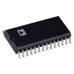
| 供应商器件封装 | 28-SSOP |
| 关闭 | Yes |
| 其它名称 | ADM3311EARSZ-REEL7DKR |
| 功能 | Transceiver |
| 包装 | Digi-Reel® |
| 协议 | RS232 |
| 双工 | 全 |
| 商标 | Analog Devices |
| 安装类型 | 表面贴装 |
| 安装风格 | SMD/SMT |
| 封装 | Reel |
| 封装/外壳 | 28-SSOP(0.209",5.30mm 宽) |
| 封装/箱体 | SSOP-28 |
| 工作温度 | -40°C ~ 85°C |
| 工作温度范围 | - 40 C to + 85 C |
| 工作电源电压 | 2.7 V to 3.6 V |
| 工厂包装数量 | 500 |
| 接收器滞后 | 140mV |
| 接收机数量 | 5 Receiver |
| 支持协议 | RS-232 |
| 数据速率 | 460Kbps |
| 最大工作温度 | + 85 C |
| 最小工作温度 | - 40 C |
| 标准包装 | 1 |
| 激励器数量 | 3 Driver |
| 电压-电源 | 2.7 V ~ 3.6 V |
| 电源电流 | 1 uA |
| 类型 | 收发器 |
| 系列 | ADM3311E |
| 驱动器/接收器数 | 3/5 |


- 商务部:美国ITC正式对集成电路等产品启动337调查
- 曝三星4nm工艺存在良率问题 高通将骁龙8 Gen1或转产台积电
- 太阳诱电将投资9.5亿元在常州建新厂生产MLCC 预计2023年完工
- 英特尔发布欧洲新工厂建设计划 深化IDM 2.0 战略
- 台积电先进制程称霸业界 有大客户加持明年业绩稳了
- 达到5530亿美元!SIA预计今年全球半导体销售额将创下新高
- 英特尔拟将自动驾驶子公司Mobileye上市 估值或超500亿美元
- 三星加码芯片和SET,合并消费电子和移动部门,撤换高东真等 CEO
- 三星电子宣布重大人事变动 还合并消费电子和移动部门
- 海关总署:前11个月进口集成电路产品价值2.52万亿元 增长14.8%


PDF Datasheet 数据手册内容提取
15 kV ESD Protected, 2.7 V to 3.6 V Serial Port Transceivers with Green Idle Data Sheet ADM3307E/ADM3310E/ADM3311E/ADM3312E/ADM3315E1 FEATURES FUNCTIONAL BLOCK DIAGRAMS Green Idle power-saving mode C1 Single 2.7 V to 3.6 V power supply 0.1µF C2 Operates with 3 V logic 0.1µF 0.1 µF to 1 µF charge pump capacitors 0.1µF C4 V+ VOLTAGE C2+ VCC CERAMIC 0.1µF TRIPLER/ LLooww pEMowI er shutdown: 20 nA TANTA1L0UµMF + CVC2C– +IN3VVETROT±E9RV CC13++ C0.31µF C1– C3– Full RS-232 compliance ENABLE EN V– 460 kb/s data rate INPUT SD GND C0.51µF One receiver active in shutdown SHUINTPDUOTWN (ADM3307E/ADM3311E/ADM3312E/ADM3315E) T1IN T1 T1OUT Two receivers active in shutdown (ADM3310E) T2IN T2 T2OUT ESD >15 kV IEC 1000-4-2 on RS-232 I/Os INPCUMTOSS1 T3IN T3 T3OUT EOIUAT/TPIUAT-2S32 ESD >15 kV IEC 1000-4-2 on CMOS and RS-232 I/Os T4IN T4 T4OUT (ADM3307E) T5IN T5 T5OUT Qualified for automotive applications R1OUT R1 R1IN APPLICATIONS OUTCPMUOTSS R2OUT R2 R2IN EINIAP/UTTIAS-2232 R3OUT R3 R3IN Mobile phone handsets/data cables ADM3307E Laptop and notebook computers PPerirniptehresr als 12IINNTTEERRNNAALL450k0ΩkPΩUPLULL-DLO-UWPNRRESEISSITSOTORR O ONNEAEACCHHCRMSO-S23 I2N PINUPTU.T. 02915-001 Modems Figure 1. ADM3307E Functional Block Diagram PDAs/Hand-Held Devices/Palmtop Computers C1 C1 0.1µF 0.1µF 0.C14µF V+ VOLTAGE C3+ C0.31µF 0.C14µF V+ VOLTAGE C3+ C0.31µF TRIPLER/ TRIPLER/ 0.1µF C2 C2+ INVERTERGND 0.1µF C2 C2+ INVERTERGND VCC C+ERAMIC 0.1µF VCC +3VTO±9V C3– VCC C+ERAMIC 0.1µF VCC +3VTO±9V C3– 10µF C2– V– C5 10µF C2– V– C5 TANTALUM ENIANBPULET EN C1– 0.1µF TANTALUM ENIANBPULET EN C1– 0.1µF C1+ SD SINHPUUTTDOWN C1+ SD SINHPUUTTDOWN T1IN T1 T1OUT T1IN T1 T1OUT INPCUMTOSS1 T2IN T2 T2OUT EOIUAT/TPIUAT-2S32 INPCUMTOSS1 T2IN T2 T2OUT EOIUAT/TPIUAT-2S32 T3IN T3 T3OUT T3IN T3 T3OUT R1OUT R1 R1IN R1OUT R1 R1IN R2OUT R2 R2IN OUTCPMUOTSS R2OUT R2 R2IN EINIAP/UTTIAS-2232 OUTCPMUOTSS R3OUT R3 R3IN EINIAP/UTTIAS-2232 R3OUT R3 R3IN R4OUT R4 R4IN ADM3312E/ R5OUT R5 R5IN ADM3315E ADM3310E/ 12IINNTTEERRNNAALL450k0ΩkPΩUPLULL-DLO-UWPNRRESEISASITSDOTMORR 3O 3ON1NE1AEEACCHHCRMSO-S23 I2N PINUPTU.T. 02915-002 12EIINNATTCEEHRRNNRAAS-LL234520k 0ΩINk(ΩP2U2PkTUΩ.LFLO-URPARDEMS3IS3T15OER) POUNLELA-DCOHWCNMROESS INISPTUOTR. ON 02915-003 Figure 2. ADM3310E/ADM3311E Functional Block Diagram Figure 3. ADM3312E/ADM3315E Functional Block Diagram 1 Protected by U.S. Patent No. 5,606,491. Rev. J Document Feedback Information furnished by Analog Devices is believed to be accurate and reliable. However, no responsibility is assumed by Analog Devices for its use, nor for any infringements of patents or other One Technology Way, P.O. Box 9106, Norwood, MA 02062-9106, U.S.A. rights of third parties that may result from its use. Specifications subject to change without notice. No license is granted by implication or otherwise under any patent or patent rights of Analog Devices. Tel: 781.329.4700 ©2002–2015 Analog Devices, Inc. All rights reserved. Trademarks and registered trademarks are the property of their respective owners. Technical Support www.analog.com
ADM3307E/ADM3310E/ADM3311E/ADM3312E/ADM3315E Data Sheet TABLE OF CONTENTS Features .............................................................................................. 1 Typical Performance Characteristics ........................................... 10 Applications ....................................................................................... 1 Circuit Description......................................................................... 13 Functional Block Diagrams ............................................................. 1 Enable and Shutdown ................................................................ 15 Revision History ............................................................................... 2 Layout and Supply Decoupling ................................................ 15 General Description ......................................................................... 3 ESD/EFT Transient Protection Scheme .................................. 15 Specifications ..................................................................................... 4 ESD Testing (IEC 1000-4-2) ..................................................... 16 Absolute Maximum Ratings ............................................................ 6 Outline Dimensions ....................................................................... 18 ESD Caution .................................................................................. 6 Ordering Guide .......................................................................... 20 Product Selection Guide .................................................................. 7 Automotive Products ................................................................. 20 Pin Configurations and Function Descriptions ........................... 8 REVISION HISTORY Edits to General Description .................................................................. 1 6/15—Rev. I to Rev. J Edits to Functional Block Diagrams ..................................................... 2 Changed ADM33xxE to ADM3307E/ADM3310E/ADM3311E/ Edits to Specifications ............................................................................... ADM3312E/ADM3315E .............................................. Throughout Edits to Absolute Maximum Ratings .................................................... 4 Changes to ESD Testing (IEC 1000-4-2) Section ....................... 16 ADM33xx Product Selection Guide Added ......................................... 5 Changes to Figure 34 ...................................................................... 17 Added ADM3307E, ADM3310E, ADM3312E, and Changes to Ordering Guide .......................................................... 20 ADM3315E Pin Configurations ............................................................ 6 Edits to Pin Function Descriptions ....................................................... 7 3/13—Rev. H to Rev. I Added ADM3307E, ADM3310E, ADM3312E, and Changed CP-32-2 Package to CP-32-7 Package, Throughout .... 1 ADM3315E Truth Tables ....................................................................... 7 Changes to Figure 4, Figure 6, Figure 8 ......................................... 8 Edits to TPCs 1–14 .................................................................................. 8 Changes to Figure 25 ...................................................................... 13 TPCs 15–18 Deleted ..............................................................................1 0 Updated Outline Dimensions ....................................................... 18 Edits to Circuit Description Section ................................................... 11 Changes to Ordering Guide .......................................................... 20 Edits to Charge Pump DC-to-DC Voltage Converter Section ........ 11 Added Automotive Products Section........................................... 20 Edits to How Does It Work Section .................................................... 11 Edits to Green Idle vs. Shutdown Section .......................................... 12 1/06—Rev. G to Rev. H Edits to Doesn’t It Increase Supply Voltage Ripple? Section ............ 12 Updated Formatting ................................................................. Universal Edits to What About Electromagnetic Compatibility? Section ....... 12 Updated Outline Dimensions .............................................................. 18 Edits to Transmitter (Driver) Section ................................................. 12 Changes to Ordering Guide ................................................................. 20 Edits to Receiver Section ...................................................................... 12 Edits to Enable and Shutdown Section ............................................... 12 4/04—Rev. F to Rev. G Edits to High Baud Rate Section.......................................................... 13 Changes to Ordering Guide ................................................................... 5 Edits to ESD/EFT Transient Protection Scheme ............................... 13 Updated Outline Dimensions .............................................................. 15 Added Figures 8a and 8b and Renumbered the Figures that Followed ..........................................................................................1 3 8/02—Rev. E to Rev. F Edits to ESD Testing (IEC 1000-4-2) Section .................................... 14 ADM3307E (REV. 0), ADM3311E (REV. E), and ADM3312E Edits to Figure 9 .....................................................................................1 4 (REV. A) Data Sheets Merged into REV. G of ADM33xxE Universal Deleted Table II and Table III and replaced them with Table V ..... 14 ADM3310E (REV. PrA Now Prelims) and ADM3315E Added RU-24 Package Outline Updated CP-32, RS-28 (REV. PrA) Added .................................................................... Universal and RU-28 ...............................................................................................1 5 Edits to Features ....................................................................................... 1 Edits to Applications ............................................................................... 1 Rev. J | Page 2 of 20
Data Sheet ADM3307E/ADM3310E/ADM3311E/ADM3312E/ADM3315E GENERAL DESCRIPTION The ADM3307E/ADM3310E/ADM3311E/ADM3312E/ The ADM3315E is a low current version of the ADM3312E, ADM3315E line of driver/receiver products is designed to fully with a 22 kΩ receiver input resistance that reduces the drive meet the EIA-232 standard while operating with a single 2.7 V requirements of the DTE. Its main applications are PDAs, to 3.6 V power supply. The devices feature an on-board charge palmtop computers, and mobile phone data lump cables. pump dc-to-dc converter, eliminating the need for dual power The ADM3307E/ADM3310E/ADM3311E/ADM3312E/ supplies. This dc-to-dc converter contains a voltage tripler and a ADM3315E devices are fabricated using CMOS technology for voltage inverter that internally generates positive and negative minimal power consumption. All parts feature a high level of supplies from the input 3 V power supply. The dc-to-dc overvoltage protection and latch-up immunity. converter operates in Green Idle™ mode, whereby the charge pump oscillator is gated on and off to maintain the output All ADM3307E/ADM3310E/ADM3311E/ADM3312E/ voltage at ±7.25 V under varying load conditions. This ADM3315E devices are available in a 32-lead 5 mm × 5 mm minimizes the power consumption and makes these products LFCSP_WQ and in a TSSOP (ADM3307E, ADM3310E, and ideal for battery-powered portable devices. ADM3311E in a 28-lead TSSOP; ADM3312E and ADM3315E in a 24-lead TSSOP). The ADM3311E also comes in a 28-lead The ADM3307E/ADM3310E/ADM3311E/ADM3312E/ SSOP. ADM3315E devices are suitable for operation in harsh electrical environments and contain ESD protection up to ±15 kV on The ADM3307E/ADM3310E/ADM3311E/ADM3312E/ their RS-232 lines (ADM3310E, ADM3311E, ADM3312E, and ADM3315E devices are ruggedized RS-232 line ADM3315E). The ADM3307E contains ESD protection up to drivers/receivers that operate from a single supply of 2.7 V to ±15 kV on all I/O lines (CMOS, RS-232, EN, and SD). 3.6 V. Step-up voltage converters coupled with level shifting transmitters and receivers allow RS-232 levels to be developed A shutdown facility that reduces the power consumption to 66 nW while operating from a single supply. Features include low is also provided. While in shutdown, one receiver remains active power consumption, Green Idle operation, high transmission (two receivers active with ADM3310E), thereby allowing monitor- rates, and compatibility with the EU directive on electromag- ing of peripheral devices. This feature allows the device to be shut netic compatibility. This EM compatibility directive includes down until a peripheral device begins communication. protection against radiated and conducted interference, The active receiver can alert the processor, which can then take including high levels of electrostatic discharge. the ADM3307E/ADM3310E/ADM3311E/ADM3312E/ All RS-232 (and CMOS, SD, and EN for ADM3307E) inputs and ADM3315E device out of the shutdown mode. outputs are protected against electrostatic discharges (up to The ADM3307E contains five drivers and three receivers and is ±15 kV). This ensures compliance with IEC 1000-4-2 intended for mobile phone data lump cables and portable requirements. computing applications. These devices are ideally suited for operation in electrically The ADM3311E contains three drivers and five receivers and is harsh environments or where RS-232 cables are frequently intended for serial port applications on notebook/laptop being plugged/unplugged. They are also immune to high RF computers. field strengths without special shielding precautions. The ADM3310E is a low current version of the ADM3311E. Emissions are also controlled to within very strict limits. CMOS This device also allows two receivers to be active in shutdown technology is used to keep the power dissipation to an absolute mode. minimum, allowing maximum battery life in portable applications. The ADM3312E contains three drivers and three receivers and is intended for serial port applications, PDAs, mobile phone data lump cables, and other hand-held devices. Rev. J | Page 3 of 20
ADM3307E/ADM3310E/ADM3311E/ADM3312E/ADM3315E Data Sheet SPECIFICATIONS V = 2.7 V to 3.6 V, C1 to C5 = 0.1 µF. All specifications T to T , unless otherwise noted. CC MIN MAX Table 1 Parameter Min Typ Max Unit Test Conditions/Comments Operating Voltage Range 2.7 3.3 3.6 V V Power Supply Current CC ADM3307E 0.75 1.5 mA V = 3.0 V to 3.6 V; no load CC 0.75 4.5 mA V = 2.7 V to 3.6 V; no load CC ADM3311E, ADM3312E 0.45 1 mA No load; V = 3.0 V to 3.6 V; T = 0°C to 85°C CC A 0.45 4.5 mA No load; V = 2.7 V to 3.6 V; T = − 40°C to +85°C CC A ADM3310E, ADM3315E 0.35 0.85 mA V = 2.7 V to 3.6 V; no load CC ADM3310E, ADM3311E, ADM3312E, 35 mA R = 3 kΩ to GND on all T L OUTS ADM3315E Shutdown Supply Current 0.02 1 µA Input Pull-Up Current 10 25 µA T = GND IN Input Leakage Current, SD, EN 0.02 ±1 µA Input Logic Threshold Low, V 0.8 V T , EN, SHDN INL IN 0.4 V T , EN, SHDN; V = 2.7 V IN CC Input Logic Threshold High, V 2.0 V T , EN, SHDN INH IN CMOS Output Voltage Low, V 0.4 V I = 1.6 mA OL OUT CMOS Output Voltage High, V V − 0.6 V I = −200 µA OH CC OUT CMOS Output Leakage Current ADM3307E 0.04 ±1 µA EN = V , 0 V < R < V CC OUT CC ADM3310E, ADM3311E 0.05 ±5 µA EN = V , 0 V < R < V CC OUT CC ADM3312E, ADM3315E Charge Pump Output Voltage, V+ +7.25 V No load ADM3307E, ADM3311E, ADM3312E Charge Pump Output Voltage, V− −7.25 V No load ADM3307E, ADM3311E, ADM3312E Charge Pump Output Voltage, V+ +6.5 V No load ADM3310E, ADM3315E Charge Pump Output Voltage, V− −6.5 V No load ADM3310E, ADM3315E EIA-232 Input Voltage Range −25 +25 V EIA-232 Input Threshold Low 0.4 1.3 V EIA-232 Input Threshold High 2.0 2.4 V EIA-232 Input Hysteresis 0.14 V EIA-232 Input Resistance ADM3307E, ADM3310E, ADM3311E, 3 5 7 kΩ ADM3312E ADM3315E 14 22 31 kΩ Output Voltage Swing ADM3310E, ADM3315E ±5.0 ±5.5 V All transmitter outputs loaded with 3 kΩ to ground ADM3307E, ADM3311E, ADM3312E ±5.0 ±6.4 V V = 3.0 V CC ±5.5 V V = 2.7 V CC All transmitter outputs loaded with 3 kΩ to ground Transmitter Output Resistance 300 Ω V = 0 V, V = ±2 V CC OUT RS-232 Output Short-Circuit Current ±15 ±60 mA Rev. J | Page 4 of 20
Data Sheet ADM3307E/ADM3310E/ADM3311E/ADM3312E/ADM3315E Parameter Min Typ Max Unit Test Conditions/Comments Maximum Data Rate ADM3307E 250 720 kbps R = 3 kΩ to 7 kΩ, C = 50 pF to 1000 pF, V = 2.7 V L L CC 460 920 kbps R = 3 kΩ to 7 kΩ, C = 50 pF to 1000 pF, V = 3.0 V L L CC ADM3310E, ADM3311E, ADM3312E, 250 460 kbps R = 3 kΩ to 7 kΩ, C = 50 pF to 1000 pF, V = 3.0 V L L CC ADM3315E Receiver Propagation Delay, T , T 0.3 µs C = 150 pF PHL PLH L 0.17 1 µs C = 150 pF; ADM3307E only L Receiver Output Enable Time, t 100 ns ER Receiver Output Disable Time, t 300 ns DR Transmitter Propagation Delay, T , T 500 ns R = 3 kΩ, C = 1000 pF PHL PLH L L Transition Region Slew Rate 3 18 V/µs R = 3 kΩ, C = 50 pF to 1000 pF1 L L ESD PROTECTION (I/O PINS) ±15 kV Human body model ±15 kV IEC 1000-4-2 air discharge ±8 kV IEC 1000-4-2 contact discharge2 1 Measured at +3 V to −3 V or −3 V to +3 V. 2 Includes CMOS I/O, SD, and EN for ADM3307E. Rev. J | Page 5 of 20
ADM3307E/ADM3310E/ADM3311E/ADM3312E/ADM3315E Data Sheet ABSOLUTE MAXIMUM RATINGS T = 25°C, unless otherwise noted. Stresses at or above those listed under Absolute Maximum A Ratings may cause permanent damage to the product. This is a Table 2 stress rating only; functional operation of the product at these Parameter Rating or any other conditions above those indicated in the operational V −0.3 V to +4 V CC section of this specification is not implied. Operation beyond V+ (V − 0.3 V) to +9 V CC the maximum operating conditions for extended periods may V− +0.3 V to −9 V affect product reliability. Input Voltages T −0.3 V to +6 V ESD CAUTION IN R ±30 V IN Output Voltages T ±15 V OUT R −0.3 V to (V + 0.3 V) OUT CC Short-Circuit Duration T Continuous OUT Thermal Impedance, θ JA LFCSP_WQ (CP-32-7) 32.5°C/W TSSOP (RU-28) 68.0°C/W TSSOP (RU-24) 68.0°C/W SSOP (RS-28) 76.0°C/W Operating Temperature Range Industrial (A Version) −40°C to +85°C Storage Temperature Range −65°C to +150°C Lead Temperature (Soldering, 10 sec) 300°C ESD Rating (IEC 1000-4-2 Air) ±15 kV (RS-232 I/Os) ESD Rating (IEC 1000-4-2 Contact) ±8 kV (RS-232 I/Os) Rev. J | Page 6 of 20
Data Sheet ADM3307E/ADM3310E/ADM3311E/ADM3312E/ADM3315E PRODUCT SELECTION GUIDE Table 3. Product Selection Guide No. Rx I CC Supply Active ICC Shutdown Generic Voltage Tx Rx in SD Speed 15 kV ESD Max Max1 Additional Features ADM3307E 2.7 V to 3.6 V 5 3 1 1 Mbps RS-232 CMOS, EN, 1.5 mA 1 µA ±15 kV ESD protection, CMOS and SD on RS-232, and CMOS I/Os including SD and EN pins ADM3310E 2.7 V to 3.6 V 3 5 2 460 kbps RS-232 0.85 mA 1 µA 2 Rxs active in shutdown, Green Idle mode level 6 V, low power ADM3311E ADM3311E 2.7 V to 3.6 V 3 5 1 460 kbps RS-232 1 mA 1 µA ADM3312E 2.7 V to 3.6 V 3 3 1 460 kbps RS-232 1 mA 1 µA ADM3315E 2.7 V to 3.6 V 3 3 1 460 kbps RS-232 0.85 mA 1 µA 22 kΩ Rx I/P resistance, Green Idle mode level 6 V, low power ADM3312E 1 I shutdown is 20 nA typically. CC Rev. J | Page 7 of 20
ADM3307E/ADM3310E/ADM3311E/ADM3312E/ADM3315E Data Sheet PIN CONFIGURATIONS AND FUNCTION DESCRIPTIONS ––C +++– 12C+2313 CCVVCCCC V+ 1 28 C2+ 21098765 33322222 VCC 2 27 C3+ EN 1 24 V– C2– 3 26 C1+ SD 2 23 GND C1– 4 25 C3– NC 3 ADM3307E 22 GND ADM3307E TTT123IIINNN 456 (NToOt Pto V SIEcaWle) 122901 TTT123OOOUUUTTT SEDN 56 (NToOtPtoVSIEcaWle) 2243 GV–ND TT45IINN 78 1178 TT45OOUUTT T1IN 7 22 T1OUT T2IN 8 21 T2OUT 901112131415161 T3IN 9 20 T3OUT CN1RTUO2RTUO3RTUOCN3RNI2RNI1RNI TT45IINN 1110 1189 TT45OOUUTT N12..O TNTHCEE S= ENXOP OCOSENDN EPCATD. IDSO C NOONTN ECCOTNENDE TCOT TGOR OTHUINSD P.IN. 02915-004 RRR312OOOUUUTTT 111234 111657 RRR321IIINNN 02915-005 Figure 4. ADM3307E LFCSP_WQ Pin Configuration Figure 5. SSOP/TSSOP Pin Configuration –2CVCC+2C+V+3CDNG–3C–V V+ 1 28 C3+ 21098765 33322222 C2+ 2 27 GND EN 1 24 C1– VCC 3 26 C3– C1+ 2 23 SD C2– 4 25 V– R1TTTON231UIIICNNNT 34567 AA(NDDToOMtM Pto33 V 3S3IE1c1aW01leEE)/ 2122129018 NTTTR123C1OOOINUUUTTT TCE11IN+N 756 AA(NDDToOMtMPto33V3S3IE1c1aW01leEE)/ 222432 CST1D1O–UT R2OUT 8 17 R2IN T2IN 8 21 T2OUT 901112131415161 T3IN 9 20 T3OUT 3TUO4TUO5TUOCNCN5RNI4RNI3RNI RR12OOUUTT 1110 1198 RR12IINN RRR R3OUT 12 17 R3IN N12..O TNTHCEE S= ENXOP OCOSENDN EPCATD. IDSO C NOONTN ECCOTNENDE TCOT TGOR OTHUINSD P.IN. 02915-006 RR45OOUUTT 1134 1165 RR45IINN 02915-007 Figure 6. LFCSP_WQ Pin Configuration Figure 7. SSOP/TSSOP Pin Configuration –2CVCC+2C+V+3CDNG–3C–V V+ 1 24 C3+ 21098765 33322222 C2+ 2 23 GND EN 1 24 C1– VCC 3 22 C3– C1+ 2 23 SD NC 3 ADM3312E/ 22 NC C2 4 ADM3312E/ 21 V– TTTN231IIICNNN 4567 A(NDToOtM Pto3 V S3IEc1aW5leE) 12219018 TTTN123COOOUUUTTT CE1N+ 56 (ANTDoOtMPto3V3SIE1cWa5lEe) 2109 SCD1– NC 8 17 NC T1IN 7 18 T1OUT 901112131415161 T2IN 8 17 T2OUT 1TUO2TUO3TUOCNCN3RNI2RNI1RNI T3IN 9 16 T3OUT RRR R1OUT 10 15 R1IN N12..O TNTHCEE S= ENXOP OCOSENDN EPCATD. IDSO C NOONTN ECCOTNENDE TCOT TGOR OTHUINSD P.IN. 02915-008 RR32OOUUTT 1121 1143 RR23IINN 02915-009 Figure 8. LFCSP_WQ Pin Configuration Figure 9. SSOP/TSSOP Pin Configuration Rev. J | Page 8 of 20
Data Sheet ADM3307E/ADM3310E/ADM3311E/ADM3312E/ADM3315E Table 4. Pin Function Descriptions Mnemonic Function VCC Power Supply Input 2.7 V to 3.6 V. V+ Internally Generated Positive Supply, 7.25 V (6.5 V Nominal for ADM3310E, ADM3315E). Capacitor C4 is connected between V and V+. CC V− Internally Generated Positive Supply, −7.25 V (−6.5 V Nominal for ADM3310E, ADM3315E). Capacitor C5 is connected between GND and V−. GND Ground Pin. Must be connected to 0 V. C1+, C1− External Capacitor 1 is connected between these pins. A 0.1 µF capacitor is recommended, but larger capacitors up to 1 µF can be used. C2+, C2− External Capacitor 2 is connected between these pins. A 0.1 µF capacitor is recommended, but larger capacitors up to 1 µF can be used. C3+, C3− External Capacitor 3 is connected between these pins. A 0.1 µF capacitor is recommended, but larger capacitors up to 1 µF can be used. TIN Transmitter (Driver) Inputs. These inputs accept TTL/CMOS levels. An internal 400 kΩ pull-up resistor to VCC is connected on each input. TOUT Transmitter (Driver) Outputs. Typically ±5.5 V (±6.4 V for ADM3311E and ADM3312E). RIN Receiver Inputs. These inputs accept RS-232 signal levels. An internal 5 kΩ pull-down resistor (22 kΩ for ADM3315E) to GND is connected on each of these inputs. ROUT Receiver Outputs. These are TTL/CMOS levels. EN Receiver Enable. A high level three-states all the receiver outputs. SD Shutdown Control. A high level disables the charge pump and reduces the quiescent current to less than 1 µA. All transmitters and most receivers are disabled. One receiver remains active in shutdown (two receivers are active in shutdown for the ADM3310E). For ADM3307E, R 3 is active in shutdown. OUT For ADM3310E, R 4 and R 5 are active in shutdown. OUT OUT For ADM3311E, R 5 is active in shutdown. OUT For ADM3312E, R 3 is active in shutdown. OUT For ADM3315E, R 3 is active in shutdown. OUT NC No Connect. Table 5. ADM3307E Truth Table Table 6. ADM3310E Truth Table SD EN Status T 1–5 R 1–2 R 3 SD EN Status T 1–3 R 1–3 R 4–5 OUT OUT OUT OUT OUT OUT 0 0 Normal Operation Enabled Enabled Enabled 0 0 Normal Operation Enabled Enabled Enabled 0 1 Normal Operation Enabled Disabled Disabled 0 1 Receivers Enabled Disabled Disabled 1 0 Shutdown Disabled Disabled Enabled Disabled 1 1 Shutdown Disabled Disabled Disabled 1 0 Shutdown Disabled Disabled Enabled 1 1 Shutdown Disabled Disabled Disabled Table 7. ADM3311E Truth Table Table 8. ADM3312E/ADM3315E Truth Table SD EN Status T 1–3 R 1–4 R 5 SD EN Status T 1–3 R 1–2 R 3 OUT OUT OUT OUT OUT OUT 0 0 Normal Operation Enabled Enabled Enabled 0 0 Normal Operation Enabled Enabled Enabled 0 1 Receivers Enabled Disabled Disabled 0 1 Normal Operation Enabled Disabled Disabled Disabled 1 0 Shutdown Disabled Disabled Enabled 1 0 Shutdown Disabled Disabled Enabled 1 1 Shutdown Disabled Disabled Disabled 1 1 Shutdown Disabled Disabled Disabled Rev. J | Page 9 of 20
ADM3307E/ADM3310E/ADM3311E/ADM3312E/ADM3315E Data Sheet TYPICAL PERFORMANCE CHARACTERISTICS 9 TOUTHIGH 7 5 3 SD P (V) V+ O/ 1 x T –1 –3 –5 TOUTLOW 02915-010 –70 200 LOAD40C0APACITAN60C0E(pF) 800 1000 02915-013 Figure 10. Charge Pump V+ Exiting Shutdown Figure 13. Transmitter Output vs. Load Capacitance (VCC = 3.3 V, Data Rate = 460 kbps) 40 35 30 s) V/µ 25 SD E ( T A 20 R W LE 15 S 10 V– 5 02915-011 00 500 LOA1D0C00APACITA1N5C0E0(pF) 2000 2500 02915-014 Figure 11. Charge Pump V− Exiting Shutdown Figure 14. Slew Rate vs. Load Capacitance (VCC = 3.3 V) 9 25 V+ 7 5 20 3 – (V) 1 mA) 15 V+/V –1 I (CC 10 –3 –5 5 V– –7 –90 5 LOADCUR10RENT(mA) 15 20 02915-012 00 200 L4O0A0DCAPA6C00ITANCE8(p00F) 1000 1200 02915-015 Figure 12. Charge Pump V+/ V− vs. Load Current (VCC = 3.3 V) Figure 15. Supply Current vs. Load Capacitance (RL = 3 kΩ) (VCC = 3.3 V, Data Rate = 460 kbps) Rev. J | Page 10 of 20
Data Sheet ADM3307E/ADM3310E/ADM3311E/ADM3312E/ADM3315E 25 20 15 A) SD m (C C I 10 5 TX O/PLOW 00 200 L4O0A0DCAPA6C00ITANCE8(0p0F) 1000 1200 02915-016 02915-019 Figure 16. Supply Current vs. Load Capacitance (RL = Infinite) Figure 19. Transmitter Output (Low) Exiting Shutdown (VCC = 3.3 V, Data Rate = 460 kbps) 30 10 28 460kbps 8 26 6 NT (mA) 2224 250kbps GE (V) 42 E A R T R 20 L 0 CU 125kbps VO UPPLY 1168 Tx OUT ––24 S 14 –6 12 –8 100 200 LOAD40C0APACITAN60C0E(pF) 800 1000 02915-017 –100 200 LOAD40C0APACITA6N0C0E(pF) 800 1000 02915-020 Figure 17. Supply Current vs. Load Capacitance (VCC = 3.3 V, RL = 5 kΩ) Figure 20. Transmitter Output Voltage High/Low vs. Load Capacitance (VCC = 3.3 V, CLK = 1 Mb/s, RL = 5 kΩ, ADM3307E) 300 Hz) 250 k Y ( NC 200 E U SD Q E TX O/P R 150 F HIGH R O T LA 100 L CI S O 50 02915-018 00 5 LOADCUR10RENT(mA) 15 20 02915-021 Figure 18. Transmitter Output (High) Exiting Shutdown Figure 21. Oscillator Frequency vs. Load Current Rev. J | Page 11 of 20
ADM3307E/ADM3310E/ADM3311E/ADM3312E/ADM3315E Data Sheet 600 25 500 20 400 15 A) A) µ m I (CC 300 I (CC 10 200 5 100 02.6 2.8 3.0 VCC(3V.)2 3.4 3.6 02915-022 02.6 2.8 3.0 VCC(3V.2) 3.4 3.6 02915-023 Figure 22. ICC vs. VCC (Unloaded) Figure 23. ICC vs. VCC (RL = 3 kΩ) Rev. J | Page 12 of 20
Data Sheet ADM3307E/ADM3310E/ADM3311E/ADM3312E/ADM3315E CIRCUIT DESCRIPTION The internal circuitry consists mainly of four sections. These During the oscillator high phase, S10 and S11 are open, while include the following: S8 and S9 are closed. C3 is charged to 3V from the output of CC the voltage tripler over several cycles. During the oscillator low • A charge pump voltage converter phase, S8 and S9 are open, while S10 and S11 are closed. C3 is • 3.3 V logic to EIA-232 transmitters connected across C5, whose positive terminal is grounded and • EIA-232 to 3.3 V logic receivers whose negative terminal is the V− output. Over several cycles, C5 charges to −3 V . CC • Transient protection circuit on all I/O lines The V+ and V− supplies may also be used to power external Charge Pump DC-to-DC Voltage Converter circuitry if the current requirements are small. See Figure 12 in The charge pump voltage converter consists of a 250 kHz (300 kHz the Typical Performance Characteristics section. for ADM3307E) oscillator and a switching matrix. The converter What Is Green Idle? generates a ±9 V supply from the input 3.0 V level. This is done in two stages using a switched capacitor technique. First, the 3.0 V Green Idle is a method of minimizing power consumption input supply is tripled to 9.0 V using Capacitor C4 as the charge under idle (no transmit) conditions while still maintaining the storage element. The +9.0 V level is then inverted to generate −9.0 ability to transmit data instantly. V using C5 as the storage element. How Does it Work? However, it should be noted that, unlike other charge pump dc- Charge pump type dc-to-dc converters used in RS-232 line to-dc converters, the charge pump on the ADM3307E does not drivers normally operate open-loop, that is, the output voltage run open-loop. The output voltage is regulated to ±7.25 V (or is not regulated in any way. Under light load conditions, the ±6.5 V for the ADM3310E and ADM3315E) by the Green Idle output voltage is close to twice the supply voltage for a doubler circuit and never reaches ±9 V in practice. This saves power as and three times the supply voltage for a tripler, with very little well as maintains a more constant output voltage. ripple. As the load current increases, the output voltage falls and the ripple voltage increases. S1 S3 S6 V+=3VCC VCC + + + Even under no-load conditions, the oscillator and charge pump C1 S5 C2 C4 GND S2 S4 S7 VCC operate at a very high frequency with consequent switching VCC losses and current drain. OISNCTIELRLANTAOLR 02915-024 Green Idle works by monitoring the output voltage and Figure 24. Charge Pump Voltage Tripler maintaining it at a constant value of around 7 V1. When the voltage rises above 7.25 V2 the oscillator is turned off. When the The tripler operates in two phases. During the oscillator low voltage falls below 7 V1, the oscillator is turned on and a burst of phase, S1 and S2 are closed and C1 charges rapidly to V . S3, CC charging pulses is sent to the reservoir capacitor. When the S4, and S5 are open, and S6 and S7 are closed. oscillator is turned off, the power consumption of the charge pump is virtually zero, so the average current drain under light During the oscillator high phase, S1 and S2 are open, and S3 load conditions is greatly reduced. and S4 are closed, so the voltage at the output of S3 is 2V . This CC voltage is used to charge C2. In the absence of any discharge current, C2 charges up to 2V after several cycles. During the CC oscillator high phase, as previously mentioned, S6 and S7 are closed, so the voltage at the output of S6 is 3VCC. This voltage is 1 For ADM3310E and ADM3315E, replace with 6.5 V. then used to charge C3. The voltage inverter is illustrated in 2 For ADM3310E and ADM3315E, replace with 6.25 V. Figure 25. S8 S10 V+ GND FROM + + VOLTAGE C3 C5 TRIPLER S9 S11 GND V– = –(V+) OISNCTIELRLANTAOLR 02915-025 Figure 25. Charge Pump Voltage Inverter Rev. J | Page 13 of 20
ADM3307E/ADM3310E/ADM3311E/ADM3312E/ADM3315E Data Sheet A block diagram of the Green Idle circuit is shown in Figure 26. Under medium load conditions, it may take several cycles for Both V+ and V− are monitored and compared to a reference C2 to charge up to 7.25 V2. The average frequency of the voltage derived from an on-chip band gap device. If either V+ oscillator is higher because there are more pulses in each burst or V− fall below 7 V1, the oscillator starts up until the voltage and the bursts of pulses are closer together and more frequent. rises above 7.25 V2. Under high load conditions, the oscillator is on continuously if the charge pump output cannot reach 7.25 V2. BAND GAP V+VOLTAGE VOLTAGE CWOMITPHA2R5A0mTOVR REFERENCE Green Idle Vs. Shutdown HYSTERESIS Shutdown mode minimizes power consumption by shutting START/STOP down the charge pump altogether. In this mode, the switches in V+ the voltage tripler are configured so V+ is connected directly to SHUTDOWN CHPUAMRGPE TRANSCEIVERS VCC. V− is zero because there is no charge pump operation to V– charge C5. This means there is a delay when coming out of shutdown mode before V+ and V− achieve their normal START/STOP operating voltages. Green Idle maintains the transmitter supply V–VOLTAGE voltages under transmitter idle conditions so this delay does not COMPARATOR HWYISTHTE2R5E0mSIVS 02915-026 Dococeusr.n ’t Green Idle Increase Supply Voltage Ripple? Figure 26. Block Diagram of Green Idle Circuit The ripple on the output voltage of a charge pump operating in The operation of Green Idle for V+ under various load open-loop depends on three factors: the oscillator frequency, conditions is illustrated in Figure 27. Under light load the value of the reservoir capacitor, and the load current. The conditions, C1 is maintained in a charged condition, and only a value of the reservoir capacitor is fixed. Increasing the oscillator single oscillator pulse is required to charge up C2. Under these frequency decreases the ripple voltage; decreasing the oscillator conditions, V+ may actually overshoot 7.25 V2 slightly. frequency increases it. Increasing the load current increases the ripple voltage; decreasing the load current decreases it. The OVERSHOOT 7.25V1 ripple voltage at light loads is naturally lower than that for high V+ load currents. 7V2 OSC Using Green Idle, the ripple voltage is determined by the high LIGHT and low thresholds of the Green Idle circuit. These are LOAD nominally 7 V1 and 7.25 V2, so the ripple is 250 mV under most 7.25V1 load conditions. With very light load conditions, there may be V+ some overshoot above 7.25 V2, so the ripple is slightly greater. 7V2 OSC Under heavy load conditions where the output never reaches 7.25 V2, the Green Idle circuit is inoperative and the ripple MEDIUM LOAD voltage is determined by the load current, the same as in a normal charge pump. 7.25V1 V+ What about Electromagnetic Compatibility? 7V2 OSC Green Idle does not operate with a constant oscillator HEAVY frequency. As a result, the frequency and spectrum of the LOAD 12FFOORRAADDMM33331100EEAANNDDAADDMM33331155EERREEPPLLAACCEEWWIITTHH66..52V5V.. 02915-027 oemsciisllsaitoonrs s aiglsnoa vl avrayr ya cwciotrhd lionagdly. .A Lnikye r oadthiaetre Ad nanaldo gc oDnedvuiccetesd Figure 27. Operation of Green Idle under Various Load Conditions RS-232 transceiver products, the ADM3307E/ADM3310E/ ADM3311E/ADM3312E/ADM3315E devices feature slew rate limiting and other techniques to minimize radiated and conducted emissions. 1 For ADM3310E and ADM3315E, replace with 6.5 V. 2 For ADM3310E and ADM3315E, replace with 6.25 V. Rev. J | Page 14 of 20
Data Sheet ADM3307E/ADM3310E/ADM3311E/ADM3312E/ADM3315E 3V Transmitter (Driver) Section EN INPUT The drivers convert 3.3 V logic input levels into EIA-232 output 0V levels. With V = 3.0 V and driving an EIA-232 load, the output CC tER voltage swing is typically ±6.4 V (or ±5.5 V for ADM3310E and VOH 3V UAnDuMse3d3 1in5pEu)t. s may be left unconnected, because an internal REOCUETIVPVEUORTL 0.4V 02915-029 Figure 29. Receiver Enable Timing 400 kV pull-up resistor pulls them high forcing the outputs into a low state. The input pull-up resistors typically source 8 mA High Baud Rate when grounded, so unused inputs should either be connected to The ADM3307E/ADM3310E/ADM3311E/ADM3312E/ V or left unconnected in order to minimize power consumption. CC ADM3315E feature high slew rates, permitting data transmission Receiver Section at rates well in excess of the EIA/RS-232E specifications. RS-232 voltage levels are maintained at data rates up to 230 kbps (460 kbps The receivers are inverting level shifters that accept RS-232 for ADM3307E) under worst-case loading conditions. This allows input levels and translate them into 3.3 V logic output levels. for high speed data links between two terminals. The inputs have internal 5 kΩ pull-down resistors (22 kΩ for the ADM3310E) to ground and are also protected against LAYOUT AND SUPPLY DECOUPLING overvoltages of up to ±30 V. Unconnected inputs are pulled to Because of the high frequencies at which the ADM3307E/ 0 V by the internal 5 kΩ (or 22 kΩ for the ADM3315E) pull- ADM3310E/ADM3311E/ADM3312E/ADM3315E oscillator down resistor. This, therefore, results in a Logic 1 output level operates, particular care should be taken with printed circuit for unconnected inputs or for inputs connected to GND. board layout, with all traces being as short as possible and C1 to The receivers have Schmitt trigger inputs with a hysteresis level C3 being connected as close to the device as possible. The use of of 0.14 V. This ensures error-free reception for both noisy a ground plane under and around the device is also highly inputs and for inputs with slow transition times. recommended. ENABLE AND SHUTDOWN When the oscillator starts up during Green Idle operation, large current pulses are taken from V . For this reason, V should The enable function is intended to facilitate data bus connections CC CC be decoupled with a parallel combination of 10 µF tantalum and where it is desirable to three-state the receiver outputs. In the 0.1 µF ceramic capacitors, mounted as close to the V pin as disabled mode, all receiver outputs are placed in a high CC possible. impedance state. The shutdown function is intended to shut the device down, thereby minimizing the quiescent current. In Capacitor C1 to Capacitor C3 can have values between 0.1 µF and shutdown, all transmitters are disabled. All receivers are shut 1 µF. Larger values give lower ripple. These capacitors can be either down, except for Receiver R3 (ADM3307E, ADM3312E, and electrolytic capacitors chosen for low equivalent series resistance ADM3315E), Receiver R5 (ADM3311E), and Receiver R4 and (ESR) or nonpolarized types, but the use of ceramic types is highly Receiver R5 (ADM3310E). Note that disabled transmitters are recommended. If polarized electrolytic capacitors are used, polarity not three-stated in shutdown, so it is not permitted to connect must be observed (as shown by C1+). multiple (RS-232) driver outputs together. ESD/EFT TRANSIENT PROTECTION SCHEME The shutdown feature is very useful in battery-operated systems The ADM3307E/ADM3310E/ADM3311E/ADM3312E/ because it reduces the power consumption to 66 nW. During ADM3315E use protective clamping structures on all inputs and shutdown, the charge pump is also disabled. When exiting outputs that clamp the voltage to a safe level and dissipate the shutdown, the charge pump is restarted and it takes approximately energy present in ESD (electrostatic) and EFT (electrical fast 100 µs for it to reach its steady-state operating conditions. transients) discharges. A simplified schematic of the protection 3V structure is shown in Figure 30 and Figure 31 (see Figure 32 and EN INPUT Figure 33 for ADM3307E protection structure). 0V tDR Each input and output contains two back-to-back high speed VOH VOH–0.1V clamping diodes. During normal operation with maximum RS-232 RECEIVER OUTPVUOTL VOL+0.1V 02915-028 sbiigansaeld l edveeplse, nthdein dgi oodne st hhea vpeo nlaor ietfyfe ocft tahs eo snieg nora lt.h Ief ,o hthoewre ivs erre,v tehres e Figure 28. Receiver Disable Timing voltage exceeds about ±50 V, reverse breakdown occurs and the voltage is clamped at this level. The diodes are large p-n junctions designed to handle the instantaneous current surge that can exceed several amperes. Rev. J | Page 15 of 20
ADM3307E/ADM3310E/ADM3311E/ADM3312E/ADM3315E Data Sheet The transmitter outputs and receiver inputs have a similar protec- ESD TESTING (IEC 1000-4-2) tion structure. The receiver inputs can also dissipate some of the IEC 1000-4-2 (previously 801-2) specifies compliance testing energy through the internal 5 kΩ (or 22 kΩ for the ADM3310E) using two coupling methods, contact discharge and air-gap resistor to GND as well as through the protection diodes. discharge. Contact discharge calls for a direct connection to the unit being tested. Airgap discharge uses a higher test voltage but does not make direct contact with the unit under testing. With RECEIVER Rx INPUT air discharge, the discharge gun is moved toward the unit under D1 RIN testing, which develops an arc across the air gap, thus the term D2 02915-030 ateirm dpiescrahtaurrgee,. bTahroism meetrtihco pdr eiss siunrfelu, edniscteadn cbey, hanumd ridatiety o, f closure Figure 30. Receiver Input Protection Scheme of the discharge gun. The contact discharge method, while less realistic, is more repeatable and is gaining acceptance in preference to the air-gap method. Tx TRANSMITTER OUTPUT D1 Although very little energy is contained within an ESD pulse, D2 the extremely fast rise time coupled with high voltages can 02915-031 cdaeustsreu fcatiilounre csa inn oucncpurro itmecmteedd sieamteliyc oans dau rcetsourlst. oCf aatracsitnrgo pohri c Figure 31. Transmitter Output Protection Scheme heating. Even if catastrophic failure does not occur immediately, The ADM3307E protection scheme is slightly different (see the device can suffer from parametric degradation that can Figure 32 and Figure 33). The receiver inputs, transmitter result in degraded performance. The cumulative effects of inputs, and transmitter outputs contain two back-to-back high continuous exposure can eventually lead to complete failure. speed clamping diodes. The receiver outputs (CMOS outputs), I/O lines are particularly vulnerable to ESD damage. Simply the SD and EN pins, contain a single reverse biased high speed touching or plugging in an I/O cable can result in a static clamping diode. Under normal operation with maximum discharge that can damage or completely destroy the interface CMOS signal levels, the receiver output, SD, and EN protection product connected to the I/O port. Traditional ESD test diodes have no effect because they are reversed biased. If, methods, such as the MIL-STD-883B method 3015.7, do not however, the voltage exceeds about 15 V, reverse breakdown fully test a product’s susceptibility to this type of discharge. This occurs and the voltage is clamped at this level. If the voltage test was intended to test a product’s susceptibility to ESD reaches −0.7 V, the diode is forward biased and the voltage is damage during handling. clamped at this level. The receiver inputs can also dissipate some of the energy through the internal 5 kΩ resistor to GND Each pin is tested with respect to ground. There are some as well as through the protection diodes. important differences between the traditional test and the IEC test. RECEIVER Rx RECEIVER The IEC test is much more stringent in terms of discharge INPUT OUTPUT D1 energy. The peak current injected is over four times RIN D3 greater. D2 02915-032 The current rise time is significantly faster in the IEC test. Figure 32. ADM3307E Receiver Input Protection Scheme The IEC test is carried out while power is applied to the device. TRANSMITTER Tx TRANSMITTER It is possible that the ESD discharge could induce latch-up in OUTPUT INPUT D3 D1 the device under test. This test, therefore, is more representative D4 D2 of a real world I/O discharge where the equipment is operating 02915-033 normally with power applied. For maximum peace of mind, Figure 33. ADM3307E Transmitter Output Protection Scheme however, both tests should be performed, ensuring maximum protection both during handling and later during field service. The protection structures achieve ESD protection up to ±15 kV on all RS-232 I/O lines (and all CMOS lines, including SD and EN for the ADM3307E). For methods used to test the protection scheme, see the ESD Testing (IEC 1000-4-2) section. Rev. J | Page 16 of 20
Data Sheet ADM3307E/ADM3310E/ADM3311E/ADM3312E/ADM3315E R1 R2 The ADM3307E/ADM3310E/ADM3311E/ADM3312E/ HIGH VOLTAGE ADM3315E devices are tested using both of the previously GENERATOR DEVICE mentioned test methods. All pins are tested with respect to all C1 UNDER TEST other pins as per the Human Body Model, ESD Assoc. Std. 55.1 specification. In addition, all I/O pins are tested as per the IEC ESD TEST METHOD R2 C1 1000-4-2 test specification. The products were tested under the HUMAN BODY MODEL I E ECS1D0 0A0S-4S-O2C. STD 55.1 13.350kΩΩ 110500ppFF 02915-034 fo llowPoinwge cr-oOndni—tioNnosr: mal Operation Figure 34. ESD Test Standards Power-Off 100 There are four levels of compliance defined by IEC 1000-4-2. 90 The ADM3307E/ADM3310E/ADM3311E/ADM3312E/ ADM3315E devices meet the most stringent compliance level for both contact and air-gap discharge. This means the products %) (K are able to withstand contact discharges in excess of 8 kV and A PE airgap discharges in excess of 15 kV. I 36.8 Table 9. IEC 1000-4-2 Compliance Levels 10 tRL tDL TIMEt 02915-035 L1e vel 2C ontact Discharge (kV) 2A ir Discharge (kV) Figure 35. Human Body Model ESD Current Waveform 2 4 4 3 6 8 100 4 8 15 90 %) (K A E P I 10 0.1ns TO 1ns TIMEt 30ns 60ns 02915-036 Figure 36. IEC1000-4-2 ESD Current Waveform Rev. J | Page 17 of 20
ADM3307E/ADM3310E/ADM3311E/ADM3312E/ADM3315E Data Sheet OUTLINE DIMENSIONS 5.10 0.30 5.00 SQ 0.25 PIN 1 4.90 0.18 INDICATOR PIN 1 25 32 INDICATOR 24 1 0.50 BSC EXPOSED 3.25 PAD 3.10 SQ 2.95 17 8 0.50 16 9 0.25 MIN TOP VIEW 0.40 BOTTOM VIEW 0.30 FOR PROPER CONNECTION OF 0.80 THE EXPOSED PAD, REFER TO 0.75 THE PIN CONFIGURATION AND 0.05 MAX FUNCTION DESCRIPTIONS 0.70 0.02 NOM SECTION OF THIS DATA SHEET. COPLANARITY 0.08 SEATING 0.20 REF PLANE COMPLIANT TO JEDEC STANDARDS MO-220-WHHD. 112408-A Figure 37. 32-Lead Lead Frame Chip Scale Package [LFCSP_WQ] 5 mm × 5 mm Body, Very Very Thin Quad (CP-32-7) Dimensions shown in millimeters 10.50 10.20 9.90 28 15 5.60 5.30 5.00 8.20 7.80 1 7.40 14 1.85 0.25 2.00 MAX 1.75 0.09 1.65 COPLA0N.0A5R MITIYN 0.65 BSC 00..3282 SPLEAATNIENG 840°°° 000...975555 0.10 COMPLIANTTO JEDEC STANDARDS MO-150-AH 060106-A Figure 38. 28-Lead Shrink Small Outline Package [SSOP] (RS-28) Dimensions shown in millimeters Rev. J | Page 18 of 20
Data Sheet ADM3307E/ADM3310E/ADM3311E/ADM3312E/ADM3315E 7.90 7.80 7.70 24 13 4.50 4.40 4.30 6.40 BSC 1 12 PIN 1 0.65 1.20 BSC MAX 0.15 0.05 8° 0.75 0.30 SEATING 0.20 0° 0.60 0.19 PLANE 0.09 0.45 0.10 COPLANARITY COMPLIANT TO JEDEC STANDARDS MO-153-AD Figure 39. 24-Lead Thin Shrink Small Outline Package [TSSOP] (RU-24) Dimensions shown in millimeters 9.80 9.70 9.60 28 15 4.50 4.40 4.30 6.40 BSC 1 14 PIN 1 0.65 BSC 1.20 MAX 0.15 0.05 8° 0.75 COPL0A.1N0ARITY 00..3109 SEPALTAINNGE 00..2009 0° 00..6405 COMPLIANT TO JEDEC STANDARDS MO-153-AE Figure 40. 28-Lead Thin Shrink Small Outline Package [TSSOP] (RU-28) Dimensions shown in millimeters Rev. J | Page 19 of 20
ADM3307E/ADM3310E/ADM3311E/ADM3312E/ADM3315E Data Sheet ORDERING GUIDE Model1, 2 Temperature Range Package Description Package Option ADM3307EARU-REEL7 −40°C to +85°C 28-Lead 7” Tape and Reel RU-28 ADM3307EARUZ −40°C to +85°C 28-Lead Thin Shrink Small Outline [TSSOP] RU-28 ADM3307EARUZ-REEL −40°C to +85°C 28-Lead 13” Tape and Reel RU-28 ADM3307EARUZ-REEL7 −40°C to +85°C 28-Lead 7” Tape and Reel RU-28 ADM3307EACPZ −40°C to +85°C 32-Lead Lead Frame Chip Scale Package [LFCSP_WQ] CP-32-7 ADM3307EACPZ-REEL −40°C to +85°C 32-Lead LFCSP_WQ 13” Tape and Reel CP-32-7 ADM3307EACPZ-REEL7 −40°C to +85°C 32-Lead LFCSP_WQ 7” Tape and Reel CP-32-7 ADM3307EWARUZ-RL7 −40°C to +85°C 28-Lead 7” Tape and Reel RU-28 ADM3310EARU −40°C to +85°C 28-Lead Thin Shrink Small Outline [TSSOP] RU-28 ADM3310EARUZ −40°C to +85°C 28-Lead Thin Shrink Small Outline [TSSOP] RU-28 ADM3310EARUZ-REEL −40°C to +85°C 28-Lead TSSOP 13” Tape and Reel RU-28 ADM3310EARUZ-REEL7 −40°C to +85°C 28-Lead TSSOP 7” Tape and Reel RU-28 ADM3310EACPZ −40°C to +85°C 32-Lead Lead Frame Chip Scale Package [LFCSP_WQ] CP-32-7 ADM3310EACPZ-REEL7 −40°C to +85°C 32-Lead LFCSP_WQ 7” Tape and Reel CP-32-7 ADM3311EARS −40°C to +85°C 28-Lead Shrink Small Outline [SSOP] RS-28 ADM3311EARSZ −40°C to +85°C 28-Lead Shrink Small Outline [SSOP] RS-28 ADM3311EARSZ-REEL −40°C to +85°C 28-Lead SSOP 13” Tape and Reel RS-28 ADM3311EARSZ-REEL7 −40°C to +85°C 28-Lead SSOP 7” Tape and Reel RS-28 ADM3311EARUZ −40°C to +85°C 28-Lead Thin Shrink Small Outline [TSSOP] RU-28 ADM3311EARUZ-REEL −40°C to +85°C 28-Lead TSSOP 13” Tape and Reel RU-28 ADM3311EARUZ-REEL7 −40°C to +85°C 28-Lead TSSOP 7” Tape and Reel RU-28 ADM3311EACPZ −40°C to +85°C 32-Lead Lead Frame Chip Scale Package [LFCSP_WQ] CP-32-7 ADM3311EACPZ-REEL7 −40°C to +85°C 32-Lead LFCSP_WQ 7” Tape and Reel CP-32-7 ADM3312EARU −40°C to +85°C 24-Lead Thin Shrink Small Outline [TSSOP] RU-24 ADM3312EARU-REEL7 −40°C to +85°C 24-Lead TSSOP 7” Tape and Reel RU-24 ADM3312EARUZ −40°C to +85°C 24-Lead Thin Shrink Small Outline [TSSOP] RU-24 ADM3312EARUZ-REEL −40°C to +85°C 24-Lead TSSOP 13” Tape and Reel RU-24 ADM3312EARUZ-REEL7 −40°C to +85°C 24-Lead TSSOP 7” Tape and Reel RU-24 ADM3312EACPZ −40°C to +85°C 32-Lead Lead Frame Chip Scale Package [LFCSP_WQ] CP-32-7 ADM3312EACPZ-REEL7 −40°C to +85°C 32-Lead LFCSP_WQ 7” Tape and Reel CP-32-7 ADM3315EARU −40°C to +85°C 24-Lead Thin Shrink Small Outline [TSSOP] RU-24 ADM3315EARU-REEL −40°C to +85°C 24-Lead TSSOP 13” Tape and Reel RU-24 ADM3315EARUZ −40°C to +85°C 24-Lead Thin Shrink Small Outline [TSSOP] RU-24 ADM3315EARUZ-REEL −40°C to +85°C 24-Lead TSSOP 13” Tape and Reel RU-24 ADM3315EARUZ-REEL7 −40°C to +85°C 24-Lead TSSOP 7” Tape and Reel RU-24 ADM3315EACPZ −40°C to +85°C 32-Lead Lead Frame Chip Scale Package [LFCSP_WQ] CP-32-7 ADM3315EACPZ-REEL −40°C to +85°C 32-Lead LFCSP_WQ 13” Tape and Reel CP-32-7 ADM3315EACPZ-REEL7 −40°C to +85°C 32-Lead LFCSP_WQ 7” Tape and Reel CP-32-7 1 Z = RoHS Compliant Part. 2 W = Qualified for Automotive Applications. AUTOMOTIVE PRODUCTS The ADM3307EW model is available with controlled manufacturing to support the quality and reliability requirements of automotive applications. Note that this automotive model may have specifications that differ from the commercial models; therefore, designers should review the Specifications section of this data sheet carefully. Only the automotive grade products shown are available for use in automotive applications. Contact your local Analog Devices account representative for specific product ordering information and to obtain the specific Automotive Reliability reports for this model. ©2002–2015 Analog Devices, Inc. All rights reserved. Trademarks and registered trademarks are the property of their respective owners. D02915-0-6/15(J) Rev. J | Page 20 of 20
Mouser Electronics Authorized Distributor Click to View Pricing, Inventory, Delivery & Lifecycle Information: A nalog Devices Inc.: ADM3311EACPZ-REEL7 ADM3315EACPZ-REEL7 ADM3311EARUZ ADM3307EARUZ-REEL7 ADM3312EARUZ- REEL7 ADM3307EACPZ-REEL ADM3307EACPZ ADM3312EACPZ-REEL ADM3315EARU ADM3311EARU ADM3307EARU-REEL7 ADM3312EARU-REEL7 ADM3310EARUZ-REEL7 ADM3312EACPZ-REEL7 ADM3315EARUZ-REEL ADM3312EACPZ ADM3310EACPZ-REEL7 ADM3311EARS ADM3311EARUZ-REEL ADM3307EARU ADM3311EARU-REEL7 ADM3311EARSZ-REEL7 ADM3315EARUZ ADM3310EARU ADM3311EARSZ ADM3312EARU ADM3310EARUZ-REEL ADM3310EARUZ ADM3315EARUZ-REEL7 ADM3307EARUZ ADM3315EACPZ ADM3311EARS-REEL7 ADM3310EACPZ-REEL ADM3307EACPZ-REEL7 ADM3311EARSZ-REEL ADM3311EARU-REEL ADM3311EACPZ-REEL ADM3311EARUZ-REEL7 ADM3312EARUZ ADM3310EACPZ ADM3311EACPZ ADM3307EARUZ-REEL ADM3312EARUZ-REEL ADM3311EARS-REEL ADM3315EACPZ-REEL