ICGOO在线商城 > 集成电路(IC) > 接口 - 驱动器,接收器,收发器 > SN65HVD35DR

 Datasheet下载
- 型号: SN65HVD35DR
- 制造商: Texas Instruments
- 库位|库存: xxxx|xxxx
- 要求:
| 数量阶梯 | 香港交货 | 国内含税 |
| +xxxx | $xxxx | ¥xxxx |
查看当月历史价格
查看今年历史价格
SN65HVD35DR产品简介:
ICGOO电子元器件商城为您提供SN65HVD35DR由Texas Instruments设计生产,在icgoo商城现货销售,并且可以通过原厂、代理商等渠道进行代购。 SN65HVD35DR价格参考¥12.54-¥25.58。Texas InstrumentsSN65HVD35DR封装/规格:接口 - 驱动器,接收器,收发器, 全 收发器 1/1 RS422,RS485 14-SOIC。您可以下载SN65HVD35DR参考资料、Datasheet数据手册功能说明书,资料中有SN65HVD35DR 详细功能的应用电路图电压和使用方法及教程。
SN65HVD35DR是德州仪器(Texas Instruments)生产的接口驱动器、接收器和收发器系列中的一款器件,主要用于CAN(Controller Area Network)物理层通信。以下是该型号的应用场景:

 1. 汽车电子
   SN65HVD35DR广泛应用于汽车电子系统中,特别是在需要可靠CAN通信的场合。例如:
   - 发动机控制单元(ECU):用于监测和控制发动机的各项参数。
   - 车身控制系统:如车窗、门锁、灯光等的控制。
   - 安全系统:如防抱死制动系统(ABS)、电子稳定程序(ESP)等。
   - 信息娱乐系统:用于音频、导航等设备之间的数据传输。

 2. 工业自动化
   在工业自动化领域,SN65HVD35DR适用于各种需要高可靠性和抗干扰能力的通信场景:
   - PLC(可编程逻辑控制器):用于工厂自动化中的数据采集与控制。
   - 传感器网络:如温度、压力、湿度等传感器的数据传输。
   - 机器人控制系统:用于机器人之间的协调工作和指令传递。

 3. 医疗设备
   医疗设备对通信的可靠性和实时性要求极高,SN65HVD35DR可以满足这些需求:
   - 监护仪:如心电图机、血压计等设备之间的数据同步。
   - 影像设备:如X光机、超声波设备的数据传输。
   - 手术室设备:确保手术过程中各设备之间的高效通信。

 4. 楼宇自动化
   楼宇自动化系统中,SN65HVD35DR可用于实现智能建筑内的设备互联:
   - 暖通空调(HVAC)系统:用于温度、通风等设备的控制。
   - 安防系统:如监控摄像头、报警系统的数据传输。
   - 照明控制系统:实现智能照明的远程控制和管理。

 5. 交通运输
   在交通运输领域,特别是铁路和公共交通系统中,SN65HVD35DR可以提供可靠的通信支持:
   - 列车控制系统:用于列车之间的通信和调度。
   - 公交管理系统:如车辆位置跟踪、乘客信息系统等。

 总结
SN65HVD35DR凭借其低功耗、高抗干扰能力和广泛的温度范围,适用于多种需要可靠CAN通信的场景,特别适合对通信质量和稳定性有严格要求的工业和汽车应用。
| 参数 | 数值 |
| 产品目录 | 集成电路 (IC)半导体 |
| 描述 | IC TXRX RS-485 3.3V 14-SOICRS-422/RS-485 接口 IC 3V Full-Dplx Driver and Receiver |
| Duplex | Full Duplex |
| 产品分类 | |
| 品牌 | Texas Instruments |
| 产品手册 | |
| 产品图片 |
|
| rohs | 符合RoHS无铅 / 符合限制有害物质指令(RoHS)规范要求 |
| 产品系列 | 接口 IC,RS-422/RS-485 接口 IC,Texas Instruments SN65HVD35DR- |
| 数据手册 | |
| 产品型号 | SN65HVD35DR |
| PCN组件/产地 | |
| 产品目录页面 | |
| 产品种类 | RS-422/RS-485 接口 IC |
| 供应商器件封装 | 14-SOIC |
| 其它名称 | 296-18706-6 |
| 功能 | Transceiver |
| 包装 | Digi-Reel® |
| 协议 | RS422,RS485 |
| 单位重量 | 133.400 mg |
| 双工 | 全 |
| 商标 | Texas Instruments |
| 安装类型 | 表面贴装 |
| 安装风格 | SMD/SMT |
| 封装 | Reel |
| 封装/外壳 | 14-SOIC(0.154",3.90mm 宽) |
| 封装/箱体 | SOIC-14 |
| 工作温度 | -40°C ~ 85°C |
| 工作温度范围 | - 40 C to + 85 C |
| 工作电源电压 | 3.3 V |
| 工厂包装数量 | 2500 |
| 接收器滞后 | 50mV |
| 接收机数量 | 1 Receiver |
| 数据速率 | 5Mbps |
| 最大工作温度 | + 85 C |
| 最小工作温度 | - 40 C |
| 标准包装 | 1 |
| 激励器数量 | 1 Driver |
| 电压-电源 | 3 V ~ 3.6 V |
| 电源电流 | 6.5 mA |
| 类型 | 收发器 |
| 系列 | SN65HVD35 |
| 驱动器/接收器数 | 1/1 |


- 商务部:美国ITC正式对集成电路等产品启动337调查
- 曝三星4nm工艺存在良率问题 高通将骁龙8 Gen1或转产台积电
- 太阳诱电将投资9.5亿元在常州建新厂生产MLCC 预计2023年完工
- 英特尔发布欧洲新工厂建设计划 深化IDM 2.0 战略
- 台积电先进制程称霸业界 有大客户加持明年业绩稳了
- 达到5530亿美元!SIA预计今年全球半导体销售额将创下新高
- 英特尔拟将自动驾驶子公司Mobileye上市 估值或超500亿美元
- 三星加码芯片和SET,合并消费电子和移动部门,撤换高东真等 CEO
- 三星电子宣布重大人事变动 还合并消费电子和移动部门
- 海关总署:前11个月进口集成电路产品价值2.52万亿元 增长14.8%


PDF Datasheet 数据手册内容提取
Product Order Technical Tools & Support & Folder Now Documents Software Community SN65HVD30,SN65HVD31,SN65HVD32 SN65HVD33,SN65HVD34,SN65HVD35 SLLS665L–SEPTEMBER2005–REVISEDJANUARY2017 SN65HVD3x 3.3-V Full-Duplex RS-485 Drivers and Receivers 1 Features 3 Description • 1/8Unit-LoadOptionAvailable The SN65HVD3x devices are 3-state differential line 1 drivers and differential-input line receivers that (Upto256NodesontheBus) operatewith3.3-Vpowersupply. • Bus-PinESDProtectionExceeds15-kVHBM Each driver and receiver has separate input and • OptionalDriverOutputTransitionTimesfor output pins for full-duplex bus communication SignalingRatesof1Mbps,5Mbpsand26Mbps designs. They are designed for RS-422 and RS-485 – LineSignalingRateistheNumberofVoltage data transmission over cable lengths of up to TransitionsMadeperSecondExpressedin 1500meters. Unitsofbps(bitspersecond) The SN65HVD30, SN65HVD31, and SN65HVD32 • Low-CurrentStandbyMode:<1μA devices are fully enabled with no external enabling • Glitch-FreePower-UpandPower-DownProtection pins. forHot-PluggingApplications The SN65HVD33, SN65HVD34, and SN65HVD35 • 5-VTolerantInputs devices have active-high driver enables and active- • BusIdle,Open,andShort-CircuitFailsafe low receiver enables. A low, less than 1 μA, standby current can be achieved by disabling both the driver • DriverCurrentLimitingandThermalShutdown andreceiver. • DesignedforRS-422andRS-485Networks All devices are characterized for ambient • 5-VDevicesAvailable,SN65HVD50-55 temperatures from –40°C to 85°C. Low power dissipation allows operation at temperatures up to 2 Applications 105°Cor125°C,dependingonpackageoption. • UtilityMeters DeviceInformation(1) • DTEandDCEInterfaces PARTNUMBER PACKAGE BODYSIZE(NOM) • Industrial,Process,andBuildingAutomation SN65HVD30 • Point-of-Sale(POS)PinsandNetworks SN65HVD31 SOIC(8) 4.90mm×3.91mm SN65HVD32 SOIC(14) 8.65mm×3.91mm SN65HVD33 VQFN(20) 4.50mm×3.50mm SN65HVD34 SOIC(14) 8.65mm×3.91mm SN65HVD35 (1) For all available packages, see the orderable addendum at theendofthedatasheet. TypicalApplicationSchematic Y A R D Z RT RT B R R DE RE Master Slave RE DE B Z D R A RT RT Y D D A B Z Y R Slave D R REDE D Copyright © 2017,Texas Instruments Incorporated 1 An IMPORTANT NOTICE at the end of this data sheet addresses availability, warranty, changes, use in safety-critical applications, intellectualpropertymattersandotherimportantdisclaimers.UNLESSOTHERWISENOTED,thisdocumentcontainsPRODUCTION DATA.
SN65HVD30,SN65HVD31,SN65HVD32 SN65HVD33,SN65HVD34,SN65HVD35 SLLS665L–SEPTEMBER2005–REVISEDJANUARY2017 www.ti.com Table of Contents 1 Features.................................................................. 1 9.1 Overview.................................................................20 2 Applications........................................................... 1 9.2 FunctionalBlockDiagram.......................................20 3 Description............................................................. 1 9.3 FeatureDescription.................................................20 9.4 DeviceFunctionalModes........................................24 4 RevisionHistory..................................................... 2 10 ApplicationandImplementation........................ 26 5 DeviceComparison............................................... 4 10.1 ApplicationInformation..........................................26 6 PinConfigurationandFunctions......................... 5 10.2 TypicalApplication ...............................................26 7 Specifications......................................................... 6 11 PowerSupplyRecommendations..................... 31 7.1 AbsoluteMaximumRatings......................................6 12 Layout................................................................... 31 7.2 ESDRatings..............................................................6 12.1 LayoutGuidelines.................................................31 7.3 RecommendedOperatingConditions.......................7 12.2 LayoutExample....................................................31 7.4 ThermalInformation..................................................7 13 DeviceandDocumentationSupport................. 32 7.5 ElectricalCharacteristics:Driver...............................8 7.6 ElectricalCharacteristics:Receiver..........................9 13.1 Third-PartyProductsDisclaimer...........................32 7.7 DevicePowerDissipation–P ................................9 13.2 RelatedLinks........................................................32 D 7.8 SupplyCurrentCharacteristics...............................10 13.3 ReceivingNotificationofDocumentationUpdates32 7.9 SwitchingCharacteristics:Driver............................10 13.4 CommunityResources..........................................32 7.10 SwitchingCharacteristics:Receiver......................11 13.5 Trademarks...........................................................32 7.11 DissipationRatings...............................................12 13.6 ElectrostaticDischargeCaution............................32 7.12 TypicalCharacteristics..........................................12 13.7 Glossary................................................................32 8 ParameterMeasurementInformation................15 14 Mechanical,Packaging,andOrderable Information........................................................... 33 9 DetailedDescription............................................ 20 4 Revision History NOTE:Pagenumbersforpreviousrevisionsmaydifferfrompagenumbersinthecurrentversion. ChangesfromRevisionK(October2015)toRevisionL Page • ChangedtextFrom:"defaultstoYhighandZlow"To:"defaultstoYlowandZhigh"intheLow-PowerStandby Modesection........................................................................................................................................................................ 20 ChangesfromRevisionJ(July2015)toRevisionK Page • ChangeddevicelistingintheDeviceInformationtabletomatchthePackageOptionAddendumlisting. ........................... 1 • ChangeddevicelistinginthePinoutConfigurationsectiontomatchthePackageOptionAddendumlisting.......................5 • ChangeddevicelistingintheThermalInformationtabletomatchthePackageOptionAddendumlisting........................... 7 ChangesfromRevisionI(April2010)toRevisionJ Page • AddedPinConfigurationandFunctionssection,ESDRatingstable,FeatureDescriptionsection,DeviceFunctional Modes,ApplicationandImplementationsection,PowerSupplyRecommendationssection,Layoutsection,Device andDocumentationSupportsection,andMechanical,Packaging,andOrderableInformationsection .............................. 1 ChangesfromRevisionH(May2009)toRevisionI Page • Changedwordingof3rdsentenceofDescription.................................................................................................................. 1 • ChangedthelabelsintheSN65HVD3xDriversOperateCorrectlyAfterBusContentionFaultsimage............................. 23 2 SubmitDocumentationFeedback Copyright©2005–2017,TexasInstrumentsIncorporated ProductFolderLinks:SN65HVD30 SN65HVD31 SN65HVD32SN65HVD33 SN65HVD34 SN65HVD35
SN65HVD30,SN65HVD31,SN65HVD32 SN65HVD33,SN65HVD34,SN65HVD35 www.ti.com SLLS665L–SEPTEMBER2005–REVISEDJANUARY2017 ChangesfromRevisionG(December2008)toRevisionH Page • Addedexplanatorynotesforpin6andpin13tothe14-PinSOIC........................................................................................ 5 • Addedexplanatorynotesforpin1andpin10tothe20-PinVQFN....................................................................................... 5 • AddedSupplycurrenttypicalvalueof3.8mAforSN65HVD31,SN65HVD3intheSupplyCurrentCharacteristicstable.10 • ChangedcharacteristicgraphforFigure6 .......................................................................................................................... 12 • ChangedcharacteristicgraphforFigure7 .......................................................................................................................... 12 • AddedsubsectionSafeOperationWithBusContention...................................................................................................... 22 ChangesfromRevisionF(July2008)toRevisionG Page • ChangedFrom:5-VDevicesAvailable,SN65HVD50-59To:5-VDevicesAvailable,SN65HVD50-55intheFeatures.......1 • DeletedSN65HVD36andSN65HVD37fromtheDescription................................................................................................ 1 • DeletedSN65HVD38andSN65HVD39fromtheDescription................................................................................................ 1 • Deletedlast2paragraphsofDescription............................................................................................................................... 1 • DeletedSN65HVD36,SN65HVD37fromthe8-PinSOIC..................................................................................................... 5 • DeletedSN65HVD36,SN65HVD37fromthethe14-PinSOIC............................................................................................. 5 • DeleteddevicesSN65HVD36,SN65HVD38fromtheRecommendedOperatingConditions............................................... 7 • DeleteddevicesSN65HVD37,SN65HVD39fromtheRecommendedOperatingConditions............................................... 7 • DeletedallHVD36,HVD38,HVD37,HVD39fromtheElectricalCharacteristics:Drivertable.............................................. 8 • Addedaddedlastsentencetonote4intheElectricalCharacteristics:Drivertable.............................................................. 8 • DeletedallHVD36,HVD38,HVD37,HVD39fromtheElectricalCharacteristics:Receivertable......................................... 9 • DeletedallHVD36,HVD38,HVD37,HVD39rowsfromtheSupplyCurrentCharacteristicstable..................................... 10 • DeletedallHVD36,HVD38,HVD37,HVD39fromtheSwitchingCharacteristics:Drivertable........................................... 10 • DeletedHVD36,HVD38,HVD37,andHVD39fromtheSwitchingCharacteristics:Receivertable.................................... 11 • DeletedReceiverEqualizationCharacteristicstable............................................................................................................ 12 • AddedsubsectionDriverOutputCurrentLimiting................................................................................................................ 21 • AddedsubsectionHot-Plugging........................................................................................................................................... 21 • AddedsubsectionReceiverFailsafe.................................................................................................................................... 22 • DeletedSN65HVD38andSN65HVD39fromTable3title................................................................................................... 24 • DeletedSN65HVD38andSN65HVD39fromTable4title................................................................................................... 24 • DeletedSN65HVD36andSN65HVD37fromTable5title................................................................................................... 24 • DeletedSN65HVD36andSN65HVD37fromTable6title................................................................................................... 24 • DeletedSN65HVD36andSN65HVD37fromfirstrowofTable7........................................................................................ 25 • DeletedSN65HVD37,SN65HVD38andSN65HVD39fromsecondrowofTable7........................................................... 25 ChangesfromRevisionE(March2008)toRevisionF Page • ChangedFrom:MeetsorExceedstheRequirementsofANSITIA/EIA-485-AandRS-422CompatibleTo:Designed forRS-422andRS-485NetworksintheFeatures................................................................................................................. 1 • AddedTableNote4intheElectricalCharacteristics:Drivertable......................................................................................... 8 ChangesfromRevisionD(January2008)toRevisionE Page • ChangedspellingFrom:termperaturesTo:temperatures..................................................................................................... 1 Copyright©2005–2017,TexasInstrumentsIncorporated SubmitDocumentationFeedback 3 ProductFolderLinks:SN65HVD30 SN65HVD31 SN65HVD32SN65HVD33 SN65HVD34 SN65HVD35
SN65HVD30,SN65HVD31,SN65HVD32 SN65HVD33,SN65HVD34,SN65HVD35 SLLS665L–SEPTEMBER2005–REVISEDJANUARY2017 www.ti.com 5 Device Comparison Table1.DeviceFeatures BASE SIGNALINGRATE UNITLOADS ENABLES PARTNUMBER SN65HVD30 26Mbps 1/2 No SN65HVD31 5Mbps 1/8 No SN65HVD32 1Mbps 1/8 No SN65HVD33 26Mbps 1/2 Yes SN65HVD34 5Mbps 1/8 Yes SN65HVD35 1Mbps 1/8 Yes Table2.ImprovedReplacementforDevices PARTNUMBER REPLACEWITH BENEFITS MAX3491 SN65HVD33 BetterESDprotection(15kVversus2kV,ornotspecified)HigherSignalingRate MAX3490 SN65HVD30 (26Mbpsversus10Mbps)FractionalUnitLoad(64Nodesversus32) MAX3491E SN65HVD33 HigherSignalingRate(26Mbpsversus12Mbps)FractionalUnitLoad(64Nodesversus32) MAX3490E SN65HVD30 MAX3076E SN65HVD33 HigherSignalingRate(26Mbpsversus16Mbps)LowerStandbyCurrent(1μAversus10μA) MAX3077E SN65HVD30 MAX3073E SN65HVD34 HigherSignalingRate(5Mbpsversus500kbps)LowerStandbyCurrent(1μAversus10μA) MAX3074E SN65HVD31 MAX3070E SN65HVD35 HigherSignalingRate(1Mbpsversus250kbps)LowerStandbyCurrent(1μAversus10μA) MAX3071E SN65HVD32 4 SubmitDocumentationFeedback Copyright©2005–2017,TexasInstrumentsIncorporated ProductFolderLinks:SN65HVD30 SN65HVD31 SN65HVD32SN65HVD33 SN65HVD34 SN65HVD35
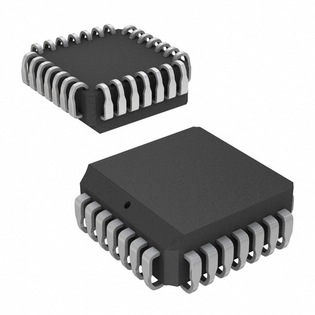
SN65HVD30,SN65HVD31,SN65HVD32 SN65HVD33,SN65HVD34,SN65HVD35 www.ti.com SLLS665L–SEPTEMBER2005–REVISEDJANUARY2017 6 Pin Configuration and Functions SN65HVD30,SN65HVD31,SN65HVD32,DPackage 8-PinSOIC SN65HVD33,SN65HVD34,SN65HVD35DPackage TopView 14-PinSOIC TopView VCC 1 8 A R 2 7 B NC 1 14 VCC D 3 6 Z R 2 13 VCC RE 3 12 A GND 4 5 Y DE 4 11 B D 5 10 Z 8 2 A GND 6 9 Y R 7 GND 7 8 NC B NC - No internal connection 5 Pins 6 and 7 are connected together internally 3 Y D 6 Pins 13 and 14 are connected together internally Z Copyright © 2017,Texas Instruments Incorporated Copyright © 2017,Texas Instruments Incorporated SN65HVD33RHLPackage 20-PinVQFN TopView V V CC CC NC 2 1 20 19 NC R A 3 18 RE 4 17 B 18 3 A NC 5 16 NC R 17 B DE 6 15 Z 4 RE D 7 14 Y 6 DE NC 8 13 NC 14 Y 7 NC 9 10 11 12 NC D 15 Z GND GND NC - No internal connection Pins 10 and 11 are connected together internally Pins 1 and 20 are connected together internally Copyright © 2017,Texas Instruments Incorporated Copyright©2005–2017,TexasInstrumentsIncorporated SubmitDocumentationFeedback 5 ProductFolderLinks:SN65HVD30 SN65HVD31 SN65HVD32SN65HVD33 SN65HVD34 SN65HVD35
SN65HVD30,SN65HVD31,SN65HVD32 SN65HVD33,SN65HVD34,SN65HVD35 SLLS665L–SEPTEMBER2005–REVISEDJANUARY2017 www.ti.com PinFunctions PIN D D RHL TYPE DESCRIPTION NAME (8-Pins) (14-Pins) (20-Pins) A 8 12 18 Businput Receiverinput(complementarytoB) B 7 11 17 Businput Receiverinput(complementarytoA) D 3 5 7 Digitalinput Driverdatainput DE — 4 6 Digitalinput Driverenable,activehigh Reference GND 4 6,7 10,11 Localdeviceground potential 2,5,8, NC — 1,8 9,12, Noconnect Noconnect;mustbeleftfloating 13,16,19 R 2 2 3 Digitaloutput Receivedataoutput RE — 3 4 Digitaloutput Receiverenable,activelow V 1 13,14 1,20 Supply 3-Vto3.6-Vsupply CC Y 5 9 14 Busoutput Driveroutput(complementarytoZ) Z 6 10 15 Busoutput Driveroutput(complementarytoY) 7 Specifications 7.1 Absolute Maximum Ratings overoperatingfree-airtemperaturerangeunlessotherwisenoted(1)(2) MIN MAX UNIT V Supplyvoltage –0.3 6 V CC V ,V , (A) (B) Voltageatanybusterminal(A,B,Y,Z) –9 14 V V ,V (Y) (Z) V Voltageinput,transientpulsethrough100Ω.SeeFigure28(A,B,Y,Z)(3) –50 50 V (TRANS) V Inputvoltage(D,DE,RE) –0.5 7 V I I Outputcurrent(receiveroutputonly,R) 11 mA O T StorageTemperature 125 °C stg (1) StressesbeyondthoselistedunderAbsoluteMaximumRatingsmaycausepermanentdamagetothedevice.Thesearestressratings only,andfunctionaloperationofthedeviceattheseoranyotherconditionsbeyondthoseindicatedunderRecommendedOperating Conditionsisnotimplied.Exposuretoabsolute-maximum-ratedconditionsforextendedperiodsmayaffectdevicereliability. (2) Allvoltagevalues,exceptdifferentialI/Obusvoltages,arewithrespecttonetworkgroundterminal. (3) Thistestssurvivabilityonlyandtheoutputstateofthereceiverisnotspecified. 7.2 ESD Ratings VALUE UNIT Humanbodymodel(HBM),perANSI/ESDA/JEDEC BuspinsandGND ±16000 V Electrostatic JS-001(1) Allpins ±4000 V (ESD) discharge Charged-devicemodel(CDM),perJEDECspecificationJESD22-C101(2) ±1000 (1) JEDECdocumentJEP155statesthat500-VHBMallowssafemanufacturingwithastandardESDcontrolprocess. (2) JEDECdocumentJEP157statesthat250-VCDMallowssafemanufacturingwithastandardESDcontrolprocess. 6 SubmitDocumentationFeedback Copyright©2005–2017,TexasInstrumentsIncorporated ProductFolderLinks:SN65HVD30 SN65HVD31 SN65HVD32SN65HVD33 SN65HVD34 SN65HVD35
SN65HVD30,SN65HVD31,SN65HVD32 SN65HVD33,SN65HVD34,SN65HVD35 www.ti.com SLLS665L–SEPTEMBER2005–REVISEDJANUARY2017 7.3 Recommended Operating Conditions overoperatingfree-airtemperaturerangeunlessotherwisenoted MIN NOM MAX UNIT V Supplyvoltage 3 3.6 V CC V orV Voltageatanybuspin(separatelyorcommonmode) –7(1) 12 V I IC SN65HVD30,SN65HVD33 26 1/t Signalingrate SN65HVD31,SN65HVD34 5 Mbps UI SN65HVD32,SN65HVD35 1 R Differentialloadresistance 54 60 Ω L V High-levelinputvoltage D,DE,RE 2 V V IH CC V Low-levelinputvoltage D,DE,RE 0 0.8 V IL V Differentialinputvoltage –12 12 V ID Driver –60 I High-leveloutputcurrent mA OH Receiver –8 Driver 60 I Low-leveloutputcurrent mA OL Receiver 8 T Junctiontemperature –40 150 °C J (1) Thealgebraicconvention,inwhichtheleastpositive(mostnegative)limitisdesignatedasminimumisusedinthisdatasheet. 7.4 Thermal Information SN65HVD30, SN65HVD33, SN65HVD31, SN65HVD34, SN65HVD33 SN65HVD32 SN65HVD35 THERMALMETRIC(1) UNIT D D RHL (SOIC) (SOIC) (VQFN) 8PINS 14PINS 20PINS R Junction-to-ambientthermalresistance 135 92 73 °C/W θJA R Junction-to-case(top)thermalresistance 43 59 14 °C/W θJC(top) R Junction-to-boardthermalresistance 44 61 13.7 °C/W θJB ψ Junction-to-topcharacterizationparameter 12.1 5.7 0.5 °C/W JT ψ Junction-to-boardcharacterizationparameter 49.7 30.7 13.7 °C/W JB R Junction-to-case(bottom)thermalresistance — — 2.8 °C/W θJC(bot) (1) Formoreinformationabouttraditionalandnewthermalmetrics,seetheSemiconductorandICPackageThermalMetricsapplication report. Copyright©2005–2017,TexasInstrumentsIncorporated SubmitDocumentationFeedback 7 ProductFolderLinks:SN65HVD30 SN65HVD31 SN65HVD32SN65HVD33 SN65HVD34 SN65HVD35
SN65HVD30,SN65HVD31,SN65HVD32 SN65HVD33,SN65HVD34,SN65HVD35 SLLS665L–SEPTEMBER2005–REVISEDJANUARY2017 www.ti.com 7.5 Electrical Characteristics: Driver overrecommendedoperatingconditionsunlessotherwisenoted PARAMETER TESTCONDITIONS MIN TYP(1) MAX UNIT V Inputclampvoltage I =–18mA –1.5 V I(K) I I =0 2.5 V O CC R =54Ω,SeeFigure17(RS-485) 1.5 2 L |V | Steady-statedifferentialoutputvoltage V OD(SS) R =100Ω,SeeFigure17,(2)(RS-422) 2 2.3 L V =–7Vto12V,SeeFigure18 1.5 test Changeinmagnitudeofsteady-state Δ|V | differentialoutputvoltagebetween R =54Ω,SeeFigure17andFigure18 –0.2 0.2 V OD(SS) L states V DifferentialOutputVoltageovershoot RL=54Ω,CL=50pF,SeeFigure21and 10%(3) V OD(RING) andundershoot Figure19 SN65HVD30, SeeFigure20 0.5 SN65HVD33 Peak-to-peak V common-mode SN65HVD31, V OC(PP) outputvoltage SN65HVD34, SeeFigure20 0.25 SN65HVD32, SN65HVD35 Steady-statecommon-modeoutput V SeeFigure20 1.6 2.3 V OC(SS) voltage Changeinsteady-statecommon-mode ΔV SeeFigure20 –0.05 0.05 V OC(SS) outputvoltage V =0V,V orV =12V, SN65HVD30, OCthCerinputaZt0VY 90 SN65HVD31, SN65HVD32 VCC=0V,VZorVY=–7V, –10 Otherinputat0V IZ(Z)or High-impedance VCC=3Vor0V,DE=0V μA IY(Z) stateoutputcurrent VZorVY=12V 90 SN65HVD33, Otherinputat0V SN65HVD34, SN65HVD35 VCC=3Vor0V,DE=0V V orV =–7V –10 Z Y Otherinputat0V V orV =–7V Z Y –250 250 IZ(S)or ShortCircuitoutputcurrent(4) Otherinputat0V mA IY(S) VZorVY=12V –250 250 Otherinputat0V I Inputcurrent D,DE 0 100 μA I C Differentialoutputcapacitance V =0.4sin(4E6πt)+0.5V,DEat0V 16 pF (OD) OD (1) Alltypicalvaluesareat25°Candwitha3.3-Vsupply. (2) V is3.3V ±5%. CC DC (3) 10%ofthepeak-to-peakdifferentialoutputvoltageswing,perTIA/EIA-485. (4) Undersomeconditionsofshort-circuittonegativevoltages,outputcurrentsexceedingtheANSITIA/EIA-485-Amaximumcurrentof250 mAmayoccur.Continuousexposurecanaffectdevicereliability.ThisappliestotheSN65HVD30,SN65HVD31,SN65HVD33,and SN65HVD34. 8 SubmitDocumentationFeedback Copyright©2005–2017,TexasInstrumentsIncorporated ProductFolderLinks:SN65HVD30 SN65HVD31 SN65HVD32SN65HVD33 SN65HVD34 SN65HVD35
SN65HVD30,SN65HVD31,SN65HVD32 SN65HVD33,SN65HVD34,SN65HVD35 www.ti.com SLLS665L–SEPTEMBER2005–REVISEDJANUARY2017 7.6 Electrical Characteristics: Receiver overrecommendedoperatingconditionsunlessotherwisenoted PARAMETER TESTCONDITIONS MIN TYP(1) MAX UNIT Positive-goingdifferentialinputthreshold V I =–8mA –0.02 V IT+ voltage O Negative-goingdifferentialinputthreshold V I =8mA –0.20 V IT- voltage O V Hysteresisvoltage(V –V ) 50 mV hys IT+ IT– V Enable-inputclampvoltage I =–18mA –1.5 V IK I V =200mV,I =–8mA,SeeFigure24 2.4 ID O V Outputvoltage V O V =–200mV,I =8mA,SeeFigure24 0.4 ID O I High-impedance-stateoutputcurrent V =0orV ,REatV –1 1 μA O(Z) O CC CC V orV =12V A B 0.05 0.1 Otherinputat0V SN65HVD31, VAorVB=12V,VCC=0V 0.06 0.1 SN65HVD32, Otherinputat0V mA SN65HVD34, V orV =–7V SN65HVD35 OAtherinBputat0V –0.10 –0.04 V orV =–7V,V =0V A B CC –0.10 –0.03 I or Otherinputat0V A Businputcurrent IB VAorVB=12V 0.20 0.35 Otherinputat0V V orV =12V,V =0V A B CC 0.24 0.4 SN65HVD30, Otherinputat0V mA SN65HVD33 V orV =–7V A B –0.35 –0.18 Otherinputat0V V orV =–7V,V =0V A B CC –0.25 –0.13 Otherinputat0V I Inputcurrent,RE V =0.8Vor2V –60 μA IH IH C Differentialinputcapacitance V =0.4sin(4E6πt)+0.5V,DEat0V 15 pF ID ID (1) Alltypicalvaluesareat25°Candwitha3.3-Vsupply. 7.7 Device Power Dissipation – P D PARAMETER TESTCONDITIONS MIN TYP MAX UNIT V =3.6V,T =140°C, SN65HVD30, CC J R =54Ω,C =50pF(driver), 197 PowerDissipation(worstcase) SN65HVD33 L L C =15pF(receiver) Driverandreceiverenabled,50%duty L cyclesquare-wavesignalatsignaling V =3.6V,T =140°C, SN65HVD31, CC J P rate: R =54Ω,C =50pF(driver), 213 mW D SN65HVD34 L L SN65HVD30,SN65HVD33at25Mbps, C =15pF(receiver) L SN65HVD31,SN65HVD34at5Mbps, V =3.6V,T =140°C, SN65HVD32,SN65HVD35at1Mbps SN65HVD32, CC J R =54Ω,C =50pF(driver), 248 SN65HVD35 L L C =15pF(receiver) L T ThermalShut-downJunctionTemperature 170 °C SD Copyright©2005–2017,TexasInstrumentsIncorporated SubmitDocumentationFeedback 9 ProductFolderLinks:SN65HVD30 SN65HVD31 SN65HVD32SN65HVD33 SN65HVD34 SN65HVD35
SN65HVD30,SN65HVD31,SN65HVD32 SN65HVD33,SN65HVD34,SN65HVD35 SLLS665L–SEPTEMBER2005–REVISEDJANUARY2017 www.ti.com 7.8 Supply Current Characteristics overrecommendedoperatingconditionsunlessotherwisenoted PARAMETER TESTCONDITIONS MIN TYP(1) MAX UNIT SN65HVD30 2.1 Dat0VorV andNoLoad mA CC SN65HVD31,SN65HVD32 3.8 6.4 SN65HVD33 REat0V,Dat0VorV ,DEat0V, 1.8 CC mA SN65HVD34,SN65HVD35 Noload(Receiverenabledanddriverdisabled) 2.2 REatV ,DatV ,DEat0V, SN65HVD33,SN65HVD34, CC CC I Supplycurrent Noload(Receiverdisabledanddriver 0.022 1 μA CC SN65HVD35 disabled) SN65HVD33 REat0V,Dat0VorV ,DEatV , 2.1 CC CC mA SN65HVD34,SN65HVD35 Noload(Receiverenabledanddriverenabled) 6.5 SN65HVD33 REatV ,Dat0VorV ,DEatV 1.8 CC CC CC mA SN65HVD34,SN65HVD35 Noload(Receiverdisabledanddriverenabled) 6.2 (1) Alltypicalvaluesareat25°Candwitha3.3-Vsupply. 7.9 Switching Characteristics: Driver overrecommendedoperatingconditionsunlessotherwisenoted PARAMETER TESTCONDITIONS MIN TYP(1) MAX UNIT SN65HVD30, 4 10 18 SN65HVD33 Propagationdelaytime,low-to-high-level SN65HVD31, t 25 38 65 ns PLH output SN65HVD34 SN65HVD32, 120 175 305 SN65HVD35 SN65HVD30, 4 9 18 SN65HVD33 Propagationdelaytime,high-to-low-level SN65HVD31, t 25 38 65 ns PHL output SN65HVD34 SN65HVD32, 120 175 305 SN65HVD35 SN65HVD30, 2.5 5 12 SN65HVD33 SN65HVD31, R =54Ω,C =50pF, t Differentialoutputsignalrisetime L L 20 37 60 ns r SN65HVD34 SeeFigure21 SN65HVD32, 120 185 300 SN65HVD35 SN65HVD30, 2.5 5 12 SN65HVD33 SN65HVD31, t Differentialoutputsignalfalltime 20 35 60 ns f SN65HVD34 SN65HVD32, 120 180 300 SN65HVD35 SN65HVD30, 0.6 SN65HVD33 SN65HVD31, t Pulseskew(|t –t |) 2.0 ns sk(p) PHL PLH SN65HVD34 SN65HVD32, 5.1 SN65HVD35 (1) Alltypicalvaluesareat25°Candwitha3.3-Vsupply. 10 SubmitDocumentationFeedback Copyright©2005–2017,TexasInstrumentsIncorporated ProductFolderLinks:SN65HVD30 SN65HVD31 SN65HVD32SN65HVD33 SN65HVD34 SN65HVD35
SN65HVD30,SN65HVD31,SN65HVD32 SN65HVD33,SN65HVD34,SN65HVD35 www.ti.com SLLS665L–SEPTEMBER2005–REVISEDJANUARY2017 Switching Characteristics: Driver (continued) overrecommendedoperatingconditionsunlessotherwisenoted PARAMETER TESTCONDITIONS MIN TYP(1) MAX UNIT SN65HVD33 45 Propagationdelaytime,high-impedance- t SN65HVD34 235 ns PZH1 to-high-leveloutput R =110Ω,REat0V, L SN65HVD35 D=3VandS1=Y,or 490 SN65HVD33 D=0VandS1=Z 25 Propagationdelaytime,high-level-to- SeeFigure22 t SN65HVD34 65 ns PHZ high-impedanceoutput SN65HVD35 165 SN65HVD33 35 Propagationdelaytime,high-impedance- t SN65HVD34 190 ns PZL1 to-low-leveloutput R =110Ω,REat0V, L SN65HVD35 D=3VandS1=Z,or 490 SN65HVD33 D=0VandS1=Y 30 Propagationdelaytime,low-level-to- SeeFigure23 t SN65HVD34 120 ns PLZ high-impedanceoutput SN65HVD35 290 t PZH1, Driverenabledelaywithbusvoltageoffset V =2V(Typ) 500 900 ns t O PZL1 R =110Ω,REat3V, L D=3VandS1=Y,or t Propagationdelaytime,standby-to-high-leveloutput 4000 ns PZH2 D=0VandS1=Z SeeFigure22 R =110Ω,REat3V, L D=3VandS1=Z,or t Propagationdelaytime,standby-to-low-leveloutput 4000 ns PZL2 D=0VandS1=Y SeeFigure23 7.10 Switching Characteristics: Receiver overrecommendedoperatingconditionsunlessotherwisenoted PARAMETER TESTCONDITIONS MIN TYP(1) MAX UNIT SN65HVD30,SN65HVD33 26 45 ns Propagationdelaytime, tPLH low-to-high-leveloutput SN65HVD31,SN65HVD32, 47 70 ns SN65HVD34,SN65HVD35 SN65HVD30,SN65HVD33 29 45 ns Propagationdelaytime, tPHL high-to-low-leveloutput SSNN6655HHVVDD3314,,SSNN6655HHVVDD3325, VID=–1.5Vto1.5V, 49 70 ns C =15pF,SeeFigure25 L SN65HVD30,SN65HVD33 7 ns tsk(p) Pulseskew(|tPHL–tPLH|) SN65HVD31,SN65HVD34, 10 ns SN65HVD32,SN65HVD35 t Outputsignalrisetime 5 ns r t Outputsignalfalltime 6 ns f t Outputdisabletimefromhighlevel 20 ns PHZ DEat3V C =15pF, t Outputenabletimetohighlevel L 20 ns PZH1 SeeFigure26 t Propagationdelaytime,standby-to-high-leveloutput DEat0V 4000 ns PZH2 t Outputdisabletimefromlowlevel 20 ns PLZ DEat3V C =15pF, t Outputenabletimetolowlevel L 20 ns PZL1 SeeFigure27 t Propagationdelaytime,standby-to-low-leveloutput DEat0V 4000 ns PZL2 (1) Alltypicalvaluesareat25°Candwitha3.3-Vsupply. Copyright©2005–2017,TexasInstrumentsIncorporated SubmitDocumentationFeedback 11 ProductFolderLinks:SN65HVD30 SN65HVD31 SN65HVD32SN65HVD33 SN65HVD34 SN65HVD35
SN65HVD30,SN65HVD31,SN65HVD32 SN65HVD33,SN65HVD34,SN65HVD35 SLLS665L–SEPTEMBER2005–REVISEDJANUARY2017 www.ti.com 7.11 Dissipation Ratings PACKAGE JEDECTHERMAL TA<25°C DERATINGFACTOR TA=85°C TA=105°C TA=125°C MODEL RATING ABOVETA=25°C RATING RATING RATING Lowk 625mW 5mW/°C 325mW 8-pinD(SOIC) Highk 1000mW 8mW/°C 520mW 360mW Lowk 765mW 6.1mW/°C 400mW 275mW 14-pinD(SOIC) Highk 1350mW 10.8mW/°C 705mW 485mW 270mW 20-pinRHL Highk 1710mW 13.7mW/°C 890mW 6150mW 340mW (VQFN) 7.12 Typical Characteristics 55 60 TA= 25°C RL= 54W TA=25°C RL= 54W RE= VCC CL= 50 pF RE= VCC CL= 50 pF DE = VCC 55 DE = VCC 50 A m A Current - 45 urrent - m 50 RMS Supply 40 VCC= 3.3 V MS Supply C 4405 VCC= 3.3 V I- CC 35 I- RCC 35 30 30 0 5 10 15 20 25 0 1 2 3 4 5 Signaling Rate - Mbps Signaling Rate - Mbps Figure1.SN65HVD30,SN65HVD33 Figure2.SN65HVD31,SN65HVD34 RMSSupplyCurrentvsSignalingRate RMSSupplyCurrentvsSignalingRate 60 250 TRAE==2 5V°CCC C RLL== 5 504 pWF 200 TDRAEE= == 2 005 °VVC 55 DE = VCC 150 A m A ent - 50 nt -m 100 Curr urre 50 I- RMS Supply CC 4405 VCC= 3.3 V I- Bus Input CI –1–05000 VCC= 3.3 V 35 –150 30 –200 0 0.2 0.4 0.6 0.8 1 –7 –4 –1 2 5 8 11 14 Signaling Rate - Mbps VI- Bus Input Voltage - V Figure3.SN65HVD32,SN65HVD35 Figure4.SN65HVD30,SN65HVD33 RMSSupplyCurrentvsSignalingRate BusInputCurrentvsInputVoltage 12 SubmitDocumentationFeedback Copyright©2005–2017,TexasInstrumentsIncorporated ProductFolderLinks:SN65HVD30 SN65HVD31 SN65HVD32SN65HVD33 SN65HVD34 SN65HVD35
SN65HVD30,SN65HVD31,SN65HVD32 SN65HVD33,SN65HVD34,SN65HVD35 www.ti.com SLLS665L–SEPTEMBER2005–REVISEDJANUARY2017 Typical Characteristics (continued) 60 3.5 TA= 25°C VCC= 3.3 V, 40 DREE == 00 VV V 3 VOH DDE = =0 VVCC, e - g 20 olta 2.5 A V s Input Current - u -200 VCC= 3.3 V - Driver Output 1.52 VOL - Bu VO 1 II -40 0.5 -60 -7 -4 -1 2 5 8 11 14 00 20 40 60 80 100 VI- Bus Input Voltage - V IO- Driver Output Current - mA Figure5.SN65HVD31,SN65HVD32,SN65HVD34, Figure6.DriverOutputVoltagevsDriverOutputCurrent SN65HVD35 BusInputCurrentvsInputVoltage 3.5 2.5 ge - V 3 100W 60W VDDCE =C =0= VV 3C.C3, V, 22..34 3.6 V RL= 60W a V Volt 2.5 ge - 2.2 Output 2 put Volta 2.1 3.3 V Driver Differential 1.15 V- Differential OutOD 111...8972 3 V - O 0.5 1.6 V 1.5 0 -60 -40 -20 0 20 40 60 80 90 0 20 40 60 80 100 IO- Driver Output Current - mA TA −Free-Air Temperature−oC Figure7.DriverDifferentialOutputVoltage Figure8.DriverDifferentialOutputVoltage vsDriverOutputCurrent vsFree-AirTemperature 40 14 T = 25°C 35 RA= 54W 13 L D = V CC A 30 DE = VCC 12 Output Current - m 2205 agation Delay - ns 1101 3 V 3.6 V I- Driver O 1105 Driver Prop 89 5 7 0 6 0 0.5 1 1.5 2 2.5 3 3.5 -60 -40 -20 0 20 40 60 80 90 VCCSupply Voltage - V TA −Free-Air Temperature−oC Figure10.SN65HVD30,SN65HVD33 Figure9.DriverOutputCurrentvsSupplyVoltage DriverPropagationDelayvsFree-AirTemperature Copyright©2005–2017,TexasInstrumentsIncorporated SubmitDocumentationFeedback 13 ProductFolderLinks:SN65HVD30 SN65HVD31 SN65HVD32SN65HVD33 SN65HVD34 SN65HVD35
SN65HVD30,SN65HVD31,SN65HVD32 SN65HVD33,SN65HVD34,SN65HVD35 SLLS665L–SEPTEMBER2005–REVISEDJANUARY2017 www.ti.com Typical Characteristics (continued) 5 0.00 −0.02 4.5 −0.04 3 V Time - ns 4 3.6 V hold−V −−00..0086 VIT+ Driver Rise/Fall 3.53 ReceiverThres −−−000...111420 VIT− −0.16 2.5 −0.18 2 −0.20 -60 -40 -20 0 20 40 60 80 90 −50 −25 0 25 50 75 100 125 TA −Free-Air Temperature−oC TA−AmbientTemperature−°C Figure11.SN65HVD30,SN65HVD33 Figure12.ReceiverThresholdvsAmbientTemperature DriverRiseandFallTimevsFree-AirTemperature 0.00 1.4 −0.02 1.2 −0.04 3.6 V V −0.06 VIT+ A 1 verThreshold− −−−000...110208 VIT− upply Current - m 00..86 3 V Recei −0.14 I- SCC 0.4 Static, −0.16 No Load 0.2 −0.18 −0.20 0 −7 −5 −3 −1 1 3 5 7 9 11 -60 -40 -20 0 20 40 60 80 90 VCM−Common-Mode Voltage−V TA −Free-Air Temperature−oC Figure13.ReceiverThresholdvsCommon-ModeVoltage Figure14.SupplyCurrentvsFree-AirTemperature 800 700 HVD35 600 ns 500 − HVD34 e m Ti 400 e bl na 300 E 200 HVD33 100 0 -7 -2 3 8 13 V(TEST)−Common-Mode Voltage−V Figure15.EnableTimevsCommon-ModeVoltage (seeFigure16) 14 SubmitDocumentationFeedback Copyright©2005–2017,TexasInstrumentsIncorporated ProductFolderLinks:SN65HVD30 SN65HVD31 SN65HVD32SN65HVD33 SN65HVD34 SN65HVD35
SN65HVD30,SN65HVD31,SN65HVD32 SN65HVD33,SN65HVD34,SN65HVD35 www.ti.com SLLS665L–SEPTEMBER2005–REVISEDJANUARY2017 8 Parameter Measurement Information 375W±1% Y -7 V < V < 12 V (TEST) D 60W V 0 or 3 V OD ±1% Z DE 375W±1% Input V 50W Generator 50% t (diff) pZH V (high) OD 1.5 V 0 V t (diff) pZL -1.5 V V (low) OD Copyright © 2017,Texas Instruments Incorporated Thetimet (x)isthemeasurefromDEtoV (x).V isvalidwhenitisgreaterthan1.5V. pZL OD OD Figure16. DriverEnableTimeFromDEtoV OD V CC II DEY IY 0 or 3 V VOD RL Z I Z V I V V Z Y Copyright © 2017,Texas Instruments Incorporated Figure17. DriverV TestCircuitandVoltageandCurrentDefinitions OD 375Ω±1% VCC DE Y D 0 or 3 V VOD 60Ω±1% + Z _ −7 V < V(test)< 12 V 375Ω±1% Copyright © 2017,Texas Instruments Incorporated Figure18. DriverV WithCommon-ModeLoadingTestCircuit OD Copyright©2005–2017,TexasInstrumentsIncorporated SubmitDocumentationFeedback 15 ProductFolderLinks:SN65HVD30 SN65HVD31 SN65HVD32SN65HVD33 SN65HVD34 SN65HVD35
SN65HVD30,SN65HVD31,SN65HVD32 SN65HVD33,SN65HVD34,SN65HVD35 SLLS665L–SEPTEMBER2005–REVISEDJANUARY2017 www.ti.com Parameter Measurement Information (continued) VOD(SS) VOD(RING) 0 V Differential VOD(RING) –VOD(SS) Figure19. V WaveformandDefinitions OD(RING) V is measured at four points on the output waveform, corresponding to overshoot and undershoot from OD(RING) theV andV steadystatevalues. OD(H) OD(L) Y VY VCC 27Ω±1% DE Z VZ Y Input D VOC(PP) ∆VOC(SS) 27Ω±1% Z VOC CL= 50 pF±20% VOC CLIncludes Fixture and Instrumentation Capacitance Input: PRR = 500 kHz, 50% Duty Cycle,tr<6ns, tf<6ns, ZO= 50Ω Copyright © 2017,Texas Instruments Incorporated Figure20. TestCircuitandDefinitionsfortheDriverCommon-ModeOutputVoltage Y » W Z W » W Copyright © 2017,Texas Instruments Incorporated Figure21. DriverSwitchingTestCircuitandVoltageWaveforms 16 SubmitDocumentationFeedback Copyright©2005–2017,TexasInstrumentsIncorporated ProductFolderLinks:SN65HVD30 SN65HVD31 SN65HVD32SN65HVD33 SN65HVD34 SN65HVD35
SN65HVD30,SN65HVD31,SN65HVD32 SN65HVD33,SN65HVD34,SN65HVD35 www.ti.com SLLS665L–SEPTEMBER2005–REVISEDJANUARY2017 Parameter Measurement Information (continued) 3 V D S1 3 V Y 0 V Z 1.5 V 1.5 V Y V I D S1 0 V VO t 0.5 V Z PZH(1 & 2) V OH Input V 50DEW CL±=2 05%0 pF RL =± 11%10 W VO 2.3 V ~ 0 V Generator I t PHZ Generator: PRR = 50 kHz, 50% Duty Cycle, t < 6 ns, t < 6 ns, Z = 50 W r f 0 C Includes Fixture and Instrumentation Capacitance L Figure22. DriverHigh-LevelOutputEnableandDisableTimeTestCircuitandVoltageWaveforms V D S1 CC 3 V Z RL= 110Ω 3 V 0 V Y ±1% Y S1 VI 1.5 V 1.5 V D VO 0 V DE Z tPZL(1&2) tPLZ Input CL= 50 pF±20% VCC Generator VI 50Ω 0.5 V VO 2.3 V VOL Generator: PRR = 50 kHz, 50% Duty Cycle, t < 6 ns, t < 6 ns, Z = 50 W r f 0 C Includes Fixture and Instrumentation Capacitance L Copyright © 2017,Texas Instruments Incorporated Figure23. DriverLow-LevelOutputEnableandDisableTimeTestCircuitandVoltageWaveforms IA A VA R IO VID B VA+ VB VIC VB IB RE VO 2 II VI Copyright © 2017,Texas Instruments Incorporated Figure24. ReceiverVoltageandCurrentDefinitions Copyright©2005–2017,TexasInstrumentsIncorporated SubmitDocumentationFeedback 17 ProductFolderLinks:SN65HVD30 SN65HVD31 SN65HVD32SN65HVD33 SN65HVD34 SN65HVD35
SN65HVD30,SN65HVD31,SN65HVD32 SN65HVD33,SN65HVD34,SN65HVD35 SLLS665L–SEPTEMBER2005–REVISEDJANUARY2017 www.ti.com Parameter Measurement Information (continued) A 3 V GeInnepruattor VI 50Ω B R VO VI 1.5 V 1.5 V 1.5 V CL= 15 pF 0 V RE ±20% tPLH tPHL 0 V VOH 90% 90% VO 1.5 V 1.5 V C Includes Fixture and Instrumentation Capacitance L 10% 10% VOL Generator: PRR = 500 kHz, 50% Duty Cycle, t r<6 ns, tf<6 ns, Zo= 50Ω tr tf Copyright © 2017,Texas Instruments Incorporated Figure25. ReceiverSwitchingTestCircuitandVoltageWaveforms V CC A 3 V 1.5 V A R VO 1 kW±1% S1 VI 1.5V 1.5V B 0 V CL= 15 pF B 0V RE ±20% tPZH(1 & 2) tPHZ GeInnepruattor VI 50 W 1.5 V VOH CLIncludes Fixture and VO 0.5V Instrumentation Capacitance ~0 V Generator: PRR = 50 kHz, 50% Duty Cycle, t < 6 ns, t < 6 ns, Z = 50 W r f 0 Copyright © 2017,Texas Instruments Incorporated Figure26. ReceiverHigh-LevelEnableandDisableTimeTestCircuitandVoltageWaveforms V CC A 3 V 0 V A R VO 1 kW±1% S1 VI 1.5V 1.5V B 1.5 V CL= 15pF B 0V RE ±20% t PZL(1 & 2) t PLZ Input V 50 W VCC Generator I C Includes Fixture VO 1.5 V 0.5V L and Instrumentation VOL Capacitance Generator: PRR = 50 kHz, 50% Duty Cycle, t < 6 ns, t < 6 ns, Z = 50 W r f 0 Copyright © 2017,Texas Instruments Incorporated Figure27. ReceiverEnableTimeFromStandby(DriverDisabled) 18 SubmitDocumentationFeedback Copyright©2005–2017,TexasInstrumentsIncorporated ProductFolderLinks:SN65HVD30 SN65HVD31 SN65HVD32SN65HVD33 SN65HVD34 SN65HVD35
SN65HVD30,SN65HVD31,SN65HVD32 SN65HVD33,SN65HVD34,SN65HVD35 www.ti.com SLLS665L–SEPTEMBER2005–REVISEDJANUARY2017 Parameter Measurement Information (continued) 0 V or 3 V DE Y A D R Z 100W 100W B RE ±1% ±1% Pulse Generator 0 V or 3 V + 15ms duration + - 1% Duty Cycle - t, t £100 ns r f Copyright © 2017,Texas Instruments Incorporated Figure28. TestCircuit,TransientOverVoltageTest Copyright©2005–2017,TexasInstrumentsIncorporated SubmitDocumentationFeedback 19 ProductFolderLinks:SN65HVD30 SN65HVD31 SN65HVD32SN65HVD33 SN65HVD34 SN65HVD35
SN65HVD30,SN65HVD31,SN65HVD32 SN65HVD33,SN65HVD34,SN65HVD35 SLLS665L–SEPTEMBER2005–REVISEDJANUARY2017 www.ti.com 9 Detailed Description 9.1 Overview The SN65HVD3x devices are low-power, full-duplex RS-485 transceivers available in three speed grades suitablefordatatransmissionof1Mbps,5Mbps,and50Mbps. The SN65HVD30, SN65HVD31, and SN65HVD32 devices are fully enabled with no external enabling pins. The SN65HVD33, SN65HVD34, and SN65HVD35 devices have active-high driver enables and active-low receiver enables.Astandbycurrentoflessthan1 µAcanbeachievedbydisablingbothdriverandreceiver. 9.2 Functional Block Diagram V V CC CC A A R R R R B B RE DE VCC Z Z D D D D Y Y GND GND a) SN65HVD33, SN65HVD34, b) SN65HVD30, SN65HVD31, SN65HVD35 SN65HVD32 Copyright © 2017,Texas Instruments Incorporated 9.3 Feature Description 9.3.1 Low-PowerStandbyMode When both the driver and receiver are disabled (DE is low and RE is high), the device is in standby mode. If the enable inputs are in this state for less than 60 ns, the device does not enter standby mode. This guards against inadvertently entering standby mode during driver or receiver enabling. The device in standby mode only when theenableinputsareheldinthisstatefor300nsormore.Inthislow-powerstandbymode,mostinternalcircuitry is powered down, and the supply current is typically less than 1 nA. When either the driver or the receiver is re- enabled,theinternalcircuitrybecomesactive. 12 A 2 R 11 B 3 RE Low-Power Standby 4 DE 9 Y 5 D 10 Z Copyright © 2017,Texas Instruments Incorporated Figure29. Low-PowerStandbyLogicDiagram If only the driver is re-enabled (DE transitions to high) the driver outputs are driven according to the D input after the enable times given by t and t in the driver switching characteristics. If the D input is open when the PZH2 PZL2 driverisenabled,thedriveroutputdefaultstoYlowandZhigh,inaccordancewiththedriver-failsafefeature. 20 SubmitDocumentationFeedback Copyright©2005–2017,TexasInstrumentsIncorporated ProductFolderLinks:SN65HVD30 SN65HVD31 SN65HVD32SN65HVD33 SN65HVD34 SN65HVD35
SN65HVD30,SN65HVD31,SN65HVD32 SN65HVD33,SN65HVD34,SN65HVD35 www.ti.com SLLS665L–SEPTEMBER2005–REVISEDJANUARY2017 Feature Description (continued) If only the receiver is re-enabled (RE transitions to low) the receiver output is driven according to the state of the bus inputs (A and B) after the enable times given by t and t in the receiver switching characteristics. If PZH2 PZL2 thereisnovalidstateonthebusthereceiverrespondsasdescribedinthefailsafeoperationsection. If both the receiver and driver are re-enabled simultaneously, the receiver output is driven according to the state of the bus inputs (A and B) and the driver output is driven according to the D input. Note that the state of the active driver affects the inputs to the receiver. Therefore, the receiver outputs are valid as soon as the driver outputsarevalid. 9.3.2 DriverOutputCurrentLimiting The RS-485 standard (ANSI/TIA/EIA-485-A or equivalently ISO 8482) specifies a 250-mA driver output current limit to prevent damage caused by data contention on the bus. That applies in the event that two or more transceivers drive the bus to opposing states at the same time. The SN65HVD3x family of devices includes current-limitingcircuitrythatpreventsdamageundertheseconditions. NOTE Thiscurrentlimitpreventsdamageduringthebuscontention,butthelogicstateofthebus canbeindeterminateasspecifiedbythestandard,socommunicationerrorscanoccur. In a specific combination of circumstances, a condition can occur in which current through the bus pin exceeds the250-mAlimit.ThiscombinationofconditionsisnotnormallyincludedinRS-485applications: • Loadingcapacitanceonthepinislessthan500pF • Thebuspinisdirectlyconnectedtoavoltagemorenegativethan –1V • ThedeviceissuppliedwithV equaltoorgreaterthan3.3V CC • Thedriverisenabled • Thebuspinisdrivingtothelogichighstate In these specific conditions, the normal current-limit circuitry and thermal-shutdown circuitry does not limit or shutdown the current flow. If the current is allowed to continue, the device heats up in a localized area near the driveroutputs,andthedevicecanbedamaged. Typical RS-485 twisted-pair cable has a capacitance of approximately 50pF/meter. Therefore, it is expected that 10metersofcablecanprovidesufficientcapacitancetopreventthislatch-upcondition. The –7 to +12-V common mode range specified by RS-485 is intended to allow communication between transceivers separated by significant distances when ground offsets may occur due to temporary current surges, electrical noise, and so on. Under those circumstances, the inherent cable needed to connect separated transceivers ensures that the conditions previously listed do not occur. For a transceiver separated by only a short cable length or backplane applications, it is unusual for there to be a steady-state negative common-mode voltage. It is possible for a negative power supply to be shorted to the bus lines due to miswiring or cable damage; however, this is a different root cause fault, and robust devices such as the SN65HVD178x family shouldbeusedforsurvivingpowersupplyormiswiringfaults. The 250-mA current limit in the RS-485 standard is intended to prevent damage caused by data contention on the bus; that is, in the event that two or more transceivers drive the bus to different states at the same time. These devices are not damaged under these conditions because all RS-485 drivers have output impedance sufficient to prevent the direct connection condition stated previously. Typical RS-485 driver output impedance is ontheorderof10Ωto30Ω. 9.3.3 Hot-Plugging These devices are designed to operate in hot swap or hot pluggable applications. Key features for hot-pluggable applicationsare: • Power-up • Power-downglitch-freeoperation • Defaultdisabledinput/outputpins • Receiverfailsafe Copyright©2005–2017,TexasInstrumentsIncorporated SubmitDocumentationFeedback 21 ProductFolderLinks:SN65HVD30 SN65HVD31 SN65HVD32SN65HVD33 SN65HVD34 SN65HVD35
SN65HVD30,SN65HVD31,SN65HVD32 SN65HVD33,SN65HVD34,SN65HVD35 SLLS665L–SEPTEMBER2005–REVISEDJANUARY2017 www.ti.com Feature Description (continued) As shown in Figure 9, an internal power-on reset circuit keeps the driver outputs in a high-impedance state until the supply voltage has reached a level at which the device reliably operates. This ensures that no spurious bits aretransmittedonthebuspinoutputsasthepowersupplyturnsonorturnsoff. As shown in the Device Functional Modes, the enable inputs have the feature of default disable on both the driver enable and receiver enable. This ensures that the device neither drives the bus nor reports data on the R pinuntiltheassociatedcontrolleractivelydrivestheenablepins. 9.3.4 ReceiverFailsafe ThedifferentialreceiversoftheSN65HVD3xfamilyarefailsafetoinvalidbusstatescausedby: • Openbusconditionssuchasadisconnectedconnector • Shortedbusconditionssuchascabledamageshortingthetwisted-pairtogether • Idlebusconditionsthatoccurwhennodriveronthebusisactivelydriving In any of these cases, the differential receiver outputs a failsafe logic high state so that the output of the receiver isnotindeterminate. Receiver failsafe is accomplished by offsetting the receiver thresholds such that the input indeterminate range does not include zero volts differential. In order to comply with the RS-422 and RS-485 standards, the receiver output must output a high when the differential input V is more positive than 200 mV, and must output a low ID when V is more negative than –200 mV. The receiver parameters which determine the failsafe performance are ID V , V , and V (the separation between V and V . As shown in the Electrical Characteristics table, IT+ IT– HYS IT+ IT– differentialsignalsmorenegativethan–200mValwayscausealowreceiveroutput,anddifferentialsignalsmore positivethan200mValwayscauseahighreceiveroutput. When the differential input signal is close to zero, it is still above the V threshold, and the receiver output is IT+ high. Only when the differential input is more than V below V does the receiver output transition to a low HYS IT+ state. Therefore, the noise immunity of the receiver inputs during a bus fault conditions includes the receiver hysteresisvalue(V )aswellasthevalueofV . HYS IT+ R VHYS 50mV VID-mV -70 -20 0 70 Vnoise-max=140mVpp Figure30. SN65HVD30-35NoiseImmunityUnderBusFaultConditions 9.3.5 SafeOperationWithBusContention These devices incorporate a driver current limit of 250 mA across the RS-485 common-mode range of –7 V to +12 V. As stated in the Application Guidelines for TIA/EIA-485-A (1), this sets a practical limitation to prevent damage during bus contention events. Contention can occur during system initialization, during system faults, or whenevertwoormoredriversareactiveatthesametime. (1) TIA/EIATelecommunicationsSystemBulletinTSB89,ApplicationGuidelinesforTIA/EIA-485-A 22 SubmitDocumentationFeedback Copyright©2005–2017,TexasInstrumentsIncorporated ProductFolderLinks:SN65HVD30 SN65HVD31 SN65HVD32SN65HVD33 SN65HVD34 SN65HVD35
SN65HVD30,SN65HVD31,SN65HVD32 SN65HVD33,SN65HVD34,SN65HVD35 www.ti.com SLLS665L–SEPTEMBER2005–REVISEDJANUARY2017 Feature Description (continued) Figure 31 shows a 2-node system to demonstrate bus contention by forcing both drivers to be active in opposing states. Vcc1 Vcc2 D ALWAYS HIGH ALWAYS ENABLED DE ±7V OFFSET GND GND 1 2 Node 1 D-pin Node 2DE-pin Bus Vdiff CONTENTION Copyright © 2017,Texas Instruments Incorporated Figure31. BusContentionExample Figure 32 shows typical operation in a bus contention event. The bottom trace illustrates how the SN65HVD33 device at Node 1 continues normal operation after a contention event between the two drivers with a –7-V ground offset on Node 2. This illustrates how the SN65HVD3x family of devices operates robustly in spite of bus contentionfaults,evenwithlargecommon-modeoffsets. Node 1 D-pin -7V offset Node 2 DE-pin Bus with intermittent contention Figure32. SN65HVD3xDriversOperateCorrectlyAfterBusContentionFaults Copyright©2005–2017,TexasInstrumentsIncorporated SubmitDocumentationFeedback 23 ProductFolderLinks:SN65HVD30 SN65HVD31 SN65HVD32SN65HVD33 SN65HVD34 SN65HVD35
SN65HVD30,SN65HVD31,SN65HVD32 SN65HVD33,SN65HVD34,SN65HVD35 SLLS665L–SEPTEMBER2005–REVISEDJANUARY2017 www.ti.com 9.4 Device Functional Modes Table3.SN65HVD33,SN65HVD34,SN65HVD35Driver INPUTS OUTPUTS D DE Y Z H H H L L H L H X Loropen Z Z Open H L H Table4.SN65HVD33,SN65HVD34,SN65HVD35 Receiver DIFFERENTIALINPUTS ENABLE OUTPUT V =V –V RE R ID (A) (B) V ≤–0.2V L L ID –0.2V<V <–0.02V L ? ID –0.02V≤V L H ID X Horopen Z OpenCircuit L H Idlecircuit L H ShortCircuit,V =V L H (A) (B) Table5.SN65HVD30,SN65HVD31,SN65HVD32Driver INPUT OUTPUTS D Y Z H H L L L H Open L H Table6.SN65HVD30,SN65HVD31,SN65HVD32 Receiver DIFFERENTIALINPUTS OUTPUT V =V –V R ID (A) (B) V ≤–0.2V L ID –0.2V<V <–0.02V ? ID –0.02V≤V H ID OpenCircuit H Idlecircuit H ShortCircuit,V =V H (A) (B) 24 SubmitDocumentationFeedback Copyright©2005–2017,TexasInstrumentsIncorporated ProductFolderLinks:SN65HVD30 SN65HVD31 SN65HVD32SN65HVD33 SN65HVD34 SN65HVD35
SN65HVD30,SN65HVD31,SN65HVD32 SN65HVD33,SN65HVD34,SN65HVD35 www.ti.com SLLS665L–SEPTEMBER2005–REVISEDJANUARY2017 REInput D and DE Input V V CC CC 130 kW 470 W 470 W Input Input 9V 9V 125 kW AInput B Input V V CC CC 22 V R1 22 V R1 R3 R3 Input Input 22 V R2 22 V R2 Yand Z Outputs R Output V V CC CC 16 V 5W Output Output 16 V 9V Copyright © 2017,Texas Instruments Incorporated Figure33. EquivalentInputandOutputSchematicDiagrams Table7.InputAttenuatorResistanceValues PARTNUMBER R1,R2 R3 SN65HVD30,SN65HVD33 9kΩ 45kΩ SN65HVD31,SN65HVD32,SN65HVD34,SN65HVD35 36kΩ 180kΩ Copyright©2005–2017,TexasInstrumentsIncorporated SubmitDocumentationFeedback 25 ProductFolderLinks:SN65HVD30 SN65HVD31 SN65HVD32SN65HVD33 SN65HVD34 SN65HVD35
SN65HVD30,SN65HVD31,SN65HVD32 SN65HVD33,SN65HVD34,SN65HVD35 SLLS665L–SEPTEMBER2005–REVISEDJANUARY2017 www.ti.com 10 Application and Implementation NOTE Information in the following applications sections is not part of the TI component specification, and TI does not warrant its accuracy or completeness. TI’s customers are responsible for determining suitability of components for their purposes. Customers should validateandtesttheirdesignimplementationtoconfirmsystemfunctionality. 10.1 Application Information The SN65HVD3x family consists of full-duplex RS-485 transceivers commonly used for asynchronous data transmissions. Full-duplex implementation requires two signal pairs (four wires), and allows each node to transmitdataononepairwhilesimultaneouslyreceivingdataontheotherpair. To eliminate line reflections, each cable end is terminated with a termination resistor (R ) whose value matches T the characteristic impedance (Z ) of the cable. This method, known as parallel termination, allows for higher data 0 ratesoverlongercablelength. Y A R D Z RT RT B R R DE RE Master Slave RE DE B Z D R A RT RT Y D D A B Z Y R Slave D R REDE D Copyright © 2017,Texas Instruments Incorporated Figure34. TypicalRS-485NetworkWithFull-DuplexTransceivers 10.2 Typical Application A full-duplex RS-485 network consists of multiple transceivers connecting in parallel to two bus cables. On one signal pair, a master driver transmits data to multiple slave receivers. The master driver and slave receivers can remain fully enabled at all times. On the other signal pair, multiple slave drivers transmit data to the master receiver. To avoid bus contention, the slave drivers must be intermittently enabled and disabled such that only one driver is enabled at any time, as in half-duplex communication. The master receiver can remain fully enabled atalltimes. Because the driver cannot be disabled, only connect one driver to the bus when using the SN65HVD30, SN65HVD31,orSN65HVD32devices. 26 SubmitDocumentationFeedback Copyright©2005–2017,TexasInstrumentsIncorporated ProductFolderLinks:SN65HVD30 SN65HVD31 SN65HVD32SN65HVD33 SN65HVD34 SN65HVD35
SN65HVD30,SN65HVD31,SN65HVD32 SN65HVD33,SN65HVD34,SN65HVD35 www.ti.com SLLS665L–SEPTEMBER2005–REVISEDJANUARY2017 Typical Application (continued) V V CC CC R A R A R R RE B RE B DE DE V CC D Z D Z D D Y Y GND GND a)Masterenable b)Slaveenable control control Copyright © 2017,Texas Instruments Incorporated Figure35. Full-DuplexTransceiverConfigurations 10.2.1 DesignRequirements RS-485 is a robust electrical standard suitable for long-distance networking that may be used in a wide range of applicationswithvaryingrequirements,suchasdistance,datarate,andnumberofnodes. 10.2.1.1 DataRateandBusLength There is an inverse relationship between data rate and bus length, meaning the higher the data rate, the shorter the cable length; and conversely, the lower the data rate, the longer the cable can be without introducing data errors. While most RS-485 systems use data rates between 10 kbps and 100 kbps, some applications require data rates up to 250 kbps at distances of 4000 feet and longer. Longer distances are possible by allowing for smallsignaljitterofupto5or10%. 10000 5%, 10%, and 20% Jitter h (ft) 1000 gt Conservative n e Characteristics L e bl 100 a C 10 100 1k 10k 100k 1M 10M 100M Data Rate(bps) Figure36. CableLengthvsDataRateCharacteristic Evenhigherdataratesareachievable(suchas26MbpsfortheSN65HVD30andSN65HVD33devices)incases where the interconnect is short enough (or has suitably low attenuation at signal frequencies) to not degrade the data. Copyright©2005–2017,TexasInstrumentsIncorporated SubmitDocumentationFeedback 27 ProductFolderLinks:SN65HVD30 SN65HVD31 SN65HVD32SN65HVD33 SN65HVD34 SN65HVD35
SN65HVD30,SN65HVD31,SN65HVD32 SN65HVD33,SN65HVD34,SN65HVD35 SLLS665L–SEPTEMBER2005–REVISEDJANUARY2017 www.ti.com Typical Application (continued) 10.2.1.2 StubLength When connecting a node to the bus, the distance between the transceiver inputs and the cable trunk, known as the stub, must be as short as possible. Stubs present a nonterminated piece of bus line that can introduce reflections as the length of the stub increases. As a general guideline, the electrical length, or round-trip delay, of a stub must be less than one-tenth of the rise time of the driver; thus giving a maximum physical stub length as showninEquation1. L ≤0.1×t ×v×c stub r where: • t isthe10/90risetimeofthedriver r • cisthespeedoflight(3×10⁸m/s) • visthesignalvelocityofthecableortraceasafactorofc (1) Per Equation 1, Table 8 shows the maximum cable-stub lengths for the minimum driver output rise times of the SN65HVD3xfull-duplexfamilyoftransceiversforasignalvelocityof78%. Table8.MaximumStubLength MINIMUMDRIVEROUTPUTRISETIME MAXIMUMSTUBLENGTH DEVICE (ns) (m) (ft) SN65HVD30 4 0.1 0.3 SN65HVD31 25 0.6 1.9 SN65HVD32 120 2.8 9.2 SN65HVD33 4 0.1 0.3 SN65HVD34 25 0.6 1.9 SN65HVD35 120 2.8 9.2 10.2.1.3 BusLoading The RS-485 standard specifies that a compliant driver must be able to driver 32 unit loads (UL), where 1 unit load represents a load impedance of approximately 12 kΩ. Because the SN65HVD30 and SN65HVD33 devices are 1/2 UL transceivers, it is possible to connect up to 64 receivers to the bus. Likewise, the SN65HVD31, SN65HVD32, SN65HVD34, and SN65HVD35 devices are 1/8 UL transceivers that can support up to 256 receivers. 28 SubmitDocumentationFeedback Copyright©2005–2017,TexasInstrumentsIncorporated ProductFolderLinks:SN65HVD30 SN65HVD31 SN65HVD32SN65HVD33 SN65HVD34 SN65HVD35
SN65HVD30,SN65HVD31,SN65HVD32 SN65HVD33,SN65HVD34,SN65HVD35 www.ti.com SLLS665L–SEPTEMBER2005–REVISEDJANUARY2017 10.2.2 DetailedDesignProcedure To protect bus nodes against high-energy transients, the implementation of external transient protection devices isnecessary(seeFigure37). 3.3 V 100nF R1 10kΩ VCC A TVS R RxD B RE DIR MCU/ R2 SN65HVD33 UART R1 DE DIR Z TVS D TxD Y 10kΩ GND R2 Copyright © 2017,Texas Instruments Incorporated Figure37. TransientProtectionAgainstESD,EFT,andSurgeTransients Table9.BillofMaterials DEVICE FUNCTION ORDERNUMBER MANUFACTURER XCVR 3.3-VFull-DuplexRS-485Transceiver SN65HVD33 TI R1,R2 10-Ω,Pulse-ProofThick-FilmResistor CRCW060310RJNEAHP Vishay TVS Bidirectional400-WTransientSuppressor CDSOT23-SM712 Bourns Copyright©2005–2017,TexasInstrumentsIncorporated SubmitDocumentationFeedback 29 ProductFolderLinks:SN65HVD30 SN65HVD31 SN65HVD32SN65HVD33 SN65HVD34 SN65HVD35
SN65HVD30,SN65HVD31,SN65HVD32 SN65HVD33,SN65HVD34,SN65HVD35 SLLS665L–SEPTEMBER2005–REVISEDJANUARY2017 www.ti.com 10.2.3 ApplicationCurve Signalsfromtoptobottom:D,Y,Z,VOD Figure38. SN65HVD33TransientWaveform 30 SubmitDocumentationFeedback Copyright©2005–2017,TexasInstrumentsIncorporated ProductFolderLinks:SN65HVD30 SN65HVD31 SN65HVD32SN65HVD33 SN65HVD34 SN65HVD35
SN65HVD30,SN65HVD31,SN65HVD32 SN65HVD33,SN65HVD34,SN65HVD35 www.ti.com SLLS665L–SEPTEMBER2005–REVISEDJANUARY2017 11 Power Supply Recommendations To ensure reliable operation at all data rates and supply voltages, each supply must be decoupled with a 100-nF ceramic capacitor located as close as possible to the supply pins. This helps to reduce supply voltage ripple present on the outputs of switched-mode power supplies and also helps compensate for the resistance andinductanceofthePCBpowerplanes. 12 Layout 12.1 Layout Guidelines Robust and reliable bus-node design often requires the use of external transient protection devices to protect against EFT and surge transients that can occur in industrial environments. Because these transients have a wide frequency bandwidth (from approximately 3 MHz to 3 GHz), high-frequency layout techniques must be appliedduringPCBdesign. • Placetheprotectioncircuitryclosetothebusconnectortopreventnoisetransientsfromenteringtheboard. • Use V and ground planes to provide low-inductance. High-frequency currents follow the path of least CC inductanceandnotthepathofleastimpedance. • Design the protection components into the direction of the signal path. Do not force the transients currents to divertfromthesignalpathtoreachtheprotectiondevice. • Apply 100-nF to 220-nF bypass capacitors as close as possible to the V pins of transceiver, UART, and CC controllerICsontheboard. • Use at least two vias for V and ground connections of bypass capacitors and protection devices to CC minimizeeffectiveviainductance. • Use 1-kΩ to 10-kΩ pullup or pulldown resistors for enable lines to limit noise currents in these lines during transientevents. • Insert series pulse-proof resistors into the A and B bus lines if the TVS clamping voltage is higher than the specifiedmaximumvoltageofthetransceiverbuspins.Theseresistorslimittheresidualclampingcurrentinto thetransceiverandpreventitfromlatchingup. • While pure TVS protection is sufficient for surge transients up to 1 kV, higher transients require metal-oxide varistors (MOVs), which reduces the transients to a few hundred volts of clamping voltage and transient blockingunits(TBUs)thatlimittransientcurrentto200mA. 12.2 Layout Example 5 C 4 Viatoground R ViatoVCC 6 R 1 R MCU 7 R R 5 TVS P 6 R M 1 J R 5 7 R R 5 TVS 5 SN65HVD33 Figure39. SN65HVD33LayoutExample Copyright©2005–2017,TexasInstrumentsIncorporated SubmitDocumentationFeedback 31 ProductFolderLinks:SN65HVD30 SN65HVD31 SN65HVD32SN65HVD33 SN65HVD34 SN65HVD35
SN65HVD30,SN65HVD31,SN65HVD32 SN65HVD33,SN65HVD34,SN65HVD35 SLLS665L–SEPTEMBER2005–REVISEDJANUARY2017 www.ti.com 13 Device and Documentation Support 13.1 Third-Party Products Disclaimer TI'S PUBLICATION OF INFORMATION REGARDING THIRD-PARTY PRODUCTS OR SERVICES DOES NOT CONSTITUTE AN ENDORSEMENT REGARDING THE SUITABILITY OF SUCH PRODUCTS OR SERVICES OR A WARRANTY, REPRESENTATION OR ENDORSEMENT OF SUCH PRODUCTS OR SERVICES, EITHER ALONEORINCOMBINATIONWITHANYTIPRODUCTORSERVICE. 13.2 Related Links The table below lists quick access links. Categories include technical documents, support and community resources,toolsandsoftware,andquickaccesstosampleorbuy. Table10.RelatedLinks TECHNICAL TOOLS& SUPPORT& PARTS PRODUCTFOLDER ORDERNOW DOCUMENTS SOFTWARE COMMUNITY SN65HVD30 Clickhere Clickhere Clickhere Clickhere Clickhere SN65HVD31 Clickhere Clickhere Clickhere Clickhere Clickhere SN65HVD32 Clickhere Clickhere Clickhere Clickhere Clickhere SN65HVD33 Clickhere Clickhere Clickhere Clickhere Clickhere SN65HVD34 Clickhere Clickhere Clickhere Clickhere Clickhere SN65HVD35 Clickhere Clickhere Clickhere Clickhere Clickhere 13.3 Receiving Notification of Documentation Updates To receive notification of documentation updates, navigate to the device product folder on ti.com. In the upper right corner, click on Alert me to register and receive a weekly digest of any product information that has changed.Forchangedetails,reviewtherevisionhistoryincludedinanyreviseddocument. 13.4 Community Resources The following links connect to TI community resources. Linked contents are provided "AS IS" by the respective contributors. They do not constitute TI specifications and do not necessarily reflect TI's views; see TI's Terms of Use. TIE2E™OnlineCommunity TI'sEngineer-to-Engineer(E2E)Community.Createdtofostercollaboration amongengineers.Ate2e.ti.com,youcanaskquestions,shareknowledge,exploreideasandhelp solveproblemswithfellowengineers. DesignSupport TI'sDesignSupport QuicklyfindhelpfulE2Eforumsalongwithdesignsupporttoolsand contactinformationfortechnicalsupport. 13.5 Trademarks E2EisatrademarkofTexasInstruments. Allothertrademarksarethepropertyoftheirrespectiveowners. 13.6 Electrostatic Discharge Caution Thesedeviceshavelimitedbuilt-inESDprotection.Theleadsshouldbeshortedtogetherorthedeviceplacedinconductivefoam duringstorageorhandlingtopreventelectrostaticdamagetotheMOSgates. 13.7 Glossary SLYZ022—TIGlossary. Thisglossarylistsandexplainsterms,acronyms,anddefinitions. 32 SubmitDocumentationFeedback Copyright©2005–2017,TexasInstrumentsIncorporated ProductFolderLinks:SN65HVD30 SN65HVD31 SN65HVD32SN65HVD33 SN65HVD34 SN65HVD35
SN65HVD30,SN65HVD31,SN65HVD32 SN65HVD33,SN65HVD34,SN65HVD35 www.ti.com SLLS665L–SEPTEMBER2005–REVISEDJANUARY2017 14 Mechanical, Packaging, and Orderable Information The following pages include mechanical, packaging, and orderable information. This information is the most current data available for the designated devices. This data is subject to change without notice and revision of thisdocument.Forbrowser-basedversionsofthisdatasheet,refertotheleft-handnavigation. Copyright©2005–2017,TexasInstrumentsIncorporated SubmitDocumentationFeedback 33 ProductFolderLinks:SN65HVD30 SN65HVD31 SN65HVD32SN65HVD33 SN65HVD34 SN65HVD35
PACKAGE OPTION ADDENDUM www.ti.com 6-Feb-2020 PACKAGING INFORMATION Orderable Device Status Package Type Package Pins Package Eco Plan Lead/Ball Finish MSL Peak Temp Op Temp (°C) Device Marking Samples (1) Drawing Qty (2) (6) (3) (4/5) SN65HVD30D ACTIVE SOIC D 8 75 Green (RoHS NIPDAU Level-1-260C-UNLIM -40 to 85 VP30 & no Sb/Br) SN65HVD30DG4 ACTIVE SOIC D 8 75 Green (RoHS NIPDAU Level-1-260C-UNLIM -40 to 85 VP30 & no Sb/Br) SN65HVD30DR ACTIVE SOIC D 8 2500 Green (RoHS NIPDAU Level-1-260C-UNLIM -40 to 85 VP30 & no Sb/Br) SN65HVD30DRG4 ACTIVE SOIC D 8 2500 Green (RoHS NIPDAU Level-1-260C-UNLIM -40 to 85 VP30 & no Sb/Br) SN65HVD31D ACTIVE SOIC D 8 75 Green (RoHS NIPDAU Level-1-260C-UNLIM -40 to 85 VP31 & no Sb/Br) SN65HVD31DG4 ACTIVE SOIC D 8 75 Green (RoHS NIPDAU Level-1-260C-UNLIM -40 to 85 VP31 & no Sb/Br) SN65HVD31DR ACTIVE SOIC D 8 2500 Green (RoHS NIPDAU Level-1-260C-UNLIM -40 to 85 VP31 & no Sb/Br) SN65HVD32D ACTIVE SOIC D 8 75 Green (RoHS NIPDAU Level-1-260C-UNLIM -40 to 85 VP32 & no Sb/Br) SN65HVD32DG4 ACTIVE SOIC D 8 75 Green (RoHS NIPDAU Level-1-260C-UNLIM -40 to 85 VP32 & no Sb/Br) SN65HVD32DR ACTIVE SOIC D 8 2500 Green (RoHS NIPDAU Level-1-260C-UNLIM -40 to 85 VP32 & no Sb/Br) SN65HVD33D ACTIVE SOIC D 14 50 Green (RoHS NIPDAU Level-1-260C-UNLIM -40 to 85 65HVD33 & no Sb/Br) SN65HVD33DG4 ACTIVE SOIC D 14 50 Green (RoHS NIPDAU Level-1-260C-UNLIM -40 to 85 65HVD33 & no Sb/Br) SN65HVD33DR ACTIVE SOIC D 14 2500 Green (RoHS NIPDAU Level-1-260C-UNLIM -40 to 85 65HVD33 & no Sb/Br) SN65HVD33DRG4 ACTIVE SOIC D 14 2500 Green (RoHS NIPDAU Level-1-260C-UNLIM -40 to 85 65HVD33 & no Sb/Br) SN65HVD33RHLR ACTIVE VQFN RHL 20 3000 Green (RoHS NIPDAU Level-2-260C-1 YEAR -40 to 85 65HVD33 & no Sb/Br) SN65HVD33RHLT ACTIVE VQFN RHL 20 250 Green (RoHS NIPDAU Level-2-260C-1 YEAR -40 to 85 65HVD33 & no Sb/Br) SN65HVD34D ACTIVE SOIC D 14 50 Green (RoHS NIPDAU Level-1-260C-UNLIM -40 to 85 65HVD34 & no Sb/Br) Addendum-Page 1
PACKAGE OPTION ADDENDUM www.ti.com 6-Feb-2020 Orderable Device Status Package Type Package Pins Package Eco Plan Lead/Ball Finish MSL Peak Temp Op Temp (°C) Device Marking Samples (1) Drawing Qty (2) (6) (3) (4/5) SN65HVD34DG4 ACTIVE SOIC D 14 50 Green (RoHS NIPDAU Level-1-260C-UNLIM -40 to 85 65HVD34 & no Sb/Br) SN65HVD34DR ACTIVE SOIC D 14 2500 Green (RoHS NIPDAU Level-1-260C-UNLIM -40 to 85 65HVD34 & no Sb/Br) SN65HVD35D ACTIVE SOIC D 14 50 Green (RoHS NIPDAU Level-1-260C-UNLIM -40 to 85 65HVD35 & no Sb/Br) SN65HVD35DG4 ACTIVE SOIC D 14 50 Green (RoHS NIPDAU Level-1-260C-UNLIM -40 to 85 65HVD35 & no Sb/Br) SN65HVD35DR ACTIVE SOIC D 14 2500 Green (RoHS NIPDAU Level-1-260C-UNLIM -40 to 85 65HVD35 & no Sb/Br) SN65HVD35DRG4 ACTIVE SOIC D 14 2500 Green (RoHS NIPDAU Level-1-260C-UNLIM -40 to 85 65HVD35 & no Sb/Br) (1) The marketing status values are defined as follows: ACTIVE: Product device recommended for new designs. LIFEBUY: TI has announced that the device will be discontinued, and a lifetime-buy period is in effect. NRND: Not recommended for new designs. Device is in production to support existing customers, but TI does not recommend using this part in a new design. PREVIEW: Device has been announced but is not in production. Samples may or may not be available. OBSOLETE: TI has discontinued the production of the device. (2) RoHS: TI defines "RoHS" to mean semiconductor products that are compliant with the current EU RoHS requirements for all 10 RoHS substances, including the requirement that RoHS substance do not exceed 0.1% by weight in homogeneous materials. Where designed to be soldered at high temperatures, "RoHS" products are suitable for use in specified lead-free processes. TI may reference these types of products as "Pb-Free". RoHS Exempt: TI defines "RoHS Exempt" to mean products that contain lead but are compliant with EU RoHS pursuant to a specific EU RoHS exemption. Green: TI defines "Green" to mean the content of Chlorine (Cl) and Bromine (Br) based flame retardants meet JS709B low halogen requirements of <=1000ppm threshold. Antimony trioxide based flame retardants must also meet the <=1000ppm threshold requirement. (3) MSL, Peak Temp. - The Moisture Sensitivity Level rating according to the JEDEC industry standard classifications, and peak solder temperature. (4) There may be additional marking, which relates to the logo, the lot trace code information, or the environmental category on the device. (5) Multiple Device Markings will be inside parentheses. Only one Device Marking contained in parentheses and separated by a "~" will appear on a device. If a line is indented then it is a continuation of the previous line and the two combined represent the entire Device Marking for that device. (6) Lead/Ball Finish - Orderable Devices may have multiple material finish options. Finish options are separated by a vertical ruled line. Lead/Ball Finish values may wrap to two lines if the finish value exceeds the maximum column width. Addendum-Page 2
PACKAGE OPTION ADDENDUM www.ti.com 6-Feb-2020 Important Information and Disclaimer:The information provided on this page represents TI's knowledge and belief as of the date that it is provided. TI bases its knowledge and belief on information provided by third parties, and makes no representation or warranty as to the accuracy of such information. Efforts are underway to better integrate information from third parties. TI has taken and continues to take reasonable steps to provide representative and accurate information but may not have conducted destructive testing or chemical analysis on incoming materials and chemicals. TI and TI suppliers consider certain information to be proprietary, and thus CAS numbers and other limited information may not be available for release. In no event shall TI's liability arising out of such information exceed the total purchase price of the TI part(s) at issue in this document sold by TI to Customer on an annual basis. OTHER QUALIFIED VERSIONS OF SN65HVD30, SN65HVD33 : •Enhanced Product: SN65HVD30-EP, SN65HVD33-EP NOTE: Qualified Version Definitions: •Enhanced Product - Supports Defense, Aerospace and Medical Applications Addendum-Page 3
PACKAGE MATERIALS INFORMATION www.ti.com 26-Feb-2019 TAPE AND REEL INFORMATION *Alldimensionsarenominal Device Package Package Pins SPQ Reel Reel A0 B0 K0 P1 W Pin1 Type Drawing Diameter Width (mm) (mm) (mm) (mm) (mm) Quadrant (mm) W1(mm) SN65HVD30DR SOIC D 8 2500 330.0 12.4 6.4 5.2 2.1 8.0 12.0 Q1 SN65HVD31DR SOIC D 8 2500 330.0 12.4 6.4 5.2 2.1 8.0 12.0 Q1 SN65HVD32DR SOIC D 8 2500 330.0 12.4 6.4 5.2 2.1 8.0 12.0 Q1 SN65HVD33RHLR VQFN RHL 20 3000 330.0 12.4 3.8 4.8 1.6 8.0 12.0 Q1 SN65HVD33RHLT VQFN RHL 20 250 180.0 12.4 3.8 4.8 1.6 8.0 12.0 Q1 SN65HVD34DR SOIC D 14 2500 330.0 16.4 6.5 9.0 2.1 8.0 16.0 Q1 SN65HVD35DR SOIC D 14 2500 330.0 16.4 6.5 9.0 2.1 8.0 16.0 Q1 PackMaterials-Page1
PACKAGE MATERIALS INFORMATION www.ti.com 26-Feb-2019 *Alldimensionsarenominal Device PackageType PackageDrawing Pins SPQ Length(mm) Width(mm) Height(mm) SN65HVD30DR SOIC D 8 2500 367.0 367.0 35.0 SN65HVD31DR SOIC D 8 2500 367.0 367.0 35.0 SN65HVD32DR SOIC D 8 2500 367.0 367.0 35.0 SN65HVD33RHLR VQFN RHL 20 3000 367.0 367.0 35.0 SN65HVD33RHLT VQFN RHL 20 250 210.0 185.0 35.0 SN65HVD34DR SOIC D 14 2500 350.0 350.0 43.0 SN65HVD35DR SOIC D 14 2500 350.0 350.0 43.0 PackMaterials-Page2
None
None
PACKAGE OUTLINE D0008A SOIC - 1.75 mm max height SCALE 2.800 SMALL OUTLINE INTEGRATED CIRCUIT C SEATING PLANE .228-.244 TYP [5.80-6.19] .004 [0.1] C A PIN 1 ID AREA 6X .050 [1.27] 8 1 2X .189-.197 [4.81-5.00] .150 NOTE 3 [3.81] 4X (0 -15 ) 4 5 8X .012-.020 B .150-.157 [0.31-0.51] .069 MAX [3.81-3.98] .010 [0.25] C A B [1.75] NOTE 4 .005-.010 TYP [0.13-0.25] 4X (0 -15 ) SEE DETAIL A .010 [0.25] .004-.010 0 - 8 [0.11-0.25] .016-.050 [0.41-1.27] DETAIL A (.041) TYPICAL [1.04] 4214825/C 02/2019 NOTES: 1. Linear dimensions are in inches [millimeters]. Dimensions in parenthesis are for reference only. Controlling dimensions are in inches. Dimensioning and tolerancing per ASME Y14.5M. 2. This drawing is subject to change without notice. 3. This dimension does not include mold flash, protrusions, or gate burrs. Mold flash, protrusions, or gate burrs shall not exceed .006 [0.15] per side. 4. This dimension does not include interlead flash. 5. Reference JEDEC registration MS-012, variation AA. www.ti.com
EXAMPLE BOARD LAYOUT D0008A SOIC - 1.75 mm max height SMALL OUTLINE INTEGRATED CIRCUIT 8X (.061 ) [1.55] SYMM SEE DETAILS 1 8 8X (.024) [0.6] SYMM (R.002 ) TYP [0.05] 5 4 6X (.050 ) [1.27] (.213) [5.4] LAND PATTERN EXAMPLE EXPOSED METAL SHOWN SCALE:8X SOLDER MASK SOLDER MASK METAL OPENING OPENING METAL UNDER SOLDER MASK EXPOSED METAL EXPOSED METAL .0028 MAX .0028 MIN [0.07] [0.07] ALL AROUND ALL AROUND NON SOLDER MASK SOLDER MASK DEFINED DEFINED SOLDER MASK DETAILS 4214825/C 02/2019 NOTES: (continued) 6. Publication IPC-7351 may have alternate designs. 7. Solder mask tolerances between and around signal pads can vary based on board fabrication site. www.ti.com
EXAMPLE STENCIL DESIGN D0008A SOIC - 1.75 mm max height SMALL OUTLINE INTEGRATED CIRCUIT 8X (.061 ) [1.55] SYMM 1 8 8X (.024) [0.6] SYMM (R.002 ) TYP [0.05] 5 4 6X (.050 ) [1.27] (.213) [5.4] SOLDER PASTE EXAMPLE BASED ON .005 INCH [0.125 MM] THICK STENCIL SCALE:8X 4214825/C 02/2019 NOTES: (continued) 8. Laser cutting apertures with trapezoidal walls and rounded corners may offer better paste release. IPC-7525 may have alternate design recommendations. 9. Board assembly site may have different recommendations for stencil design. www.ti.com
None
PACKAGE OUTLINE RHL0020A VQFN - 1 mm max height PLASTIC QUAD FLATPACK- NO LEAD 3.6 A B 3.4 PIN 1 INDEX AREA 4.6 4.4 C 1 MAX SEATING PLANE 0.08 C 2.05±0.1 2X 1.5 0.5 SYMM 20X 0.3 (0.2) TYP 10 11 14X 0.5 9 12 2X SYMM 21 3.5 3.05±0.1 19 2 0.29 20X 1 20 0.19 PIN 1 ID (OPTIONAL) 4X (0.2) 0.1 C A B 0.05 C 2X (0.55) 4219071 / A 05/2017 NOTES: 1. All linear dimensions are in millimeters. Any dimensions in parenthesis are for reference only. Dimensioning and tolerancing per ASME Y14.5M. 2. This drawing is subject to change without notice. 3. The package thermal pad must be soldered to the printed circuit board for thermal and mechanical performance. www.ti.com
EXAMPLE BOARD LAYOUT RHL0020A VQFN - 1 mm max height PLASTIC QUAD FLATPACK- NO LEAD (3.3) (2.05) 2X (1.5) SYMM 1 20 2X (0.4) 20X (0.6) 2 19 20X (0.24) 14X (0.5) SYMM 21 (3.05) (4.3) 6X (0.525) 2X (0.75) SOLDER MASK OPENING METAL UNDER SOLDER MASK 9 12 (R0.05) TYP (Ø0.2) VIA 10 11 TYP) 4X (0.2) 4X (0.775) 2X (0.55) LAND PATTERN EXAMPLE EXPOSED METAL SHOWN SCALE: 18X 0.07 MAX 0.07 MIN SOLDER MASK ALL AROUND ALL AROUND OPENING EXPOSED METAL EXPOSED METAL METAL METAL UNDER SOLDER MASK SOLDER MASK OPENING NON SOLDER MASK SOLDER MASK DEFINED DEFINED (PREFERRED) SOLDER MASK DETAILS 4219071 / A 05/2017 NOTES: (continued) 4. This package is designed to be soldered to a thermal pad on the board. For more information, see Texas Instruments literature number SLUA271 (www.ti.com/lit/slua271). 5. Solder mask tolerances between and around signal pads can vary based on board fabrication site. 6. Vias are optional depending on application, refer to device data sheet. If any vias are implemented, refer to theri locations shown on this view. It is recommended that vias under paste be filled, plugged or tented. www.ti.com
EXAMPLE STENCIL DESIGN RHL0020A VQFN - 1 mm max height PLASTIC QUAD FLATPACK- NO LEAD (3.3) 2X (1.5) (0.55) TYP (0.56) TYP 1 20 SOLDER MASK EDGE TYP 20X (0.6) 2 19 20X (0.24) 14X (0.5) (1.05) TYP SYMM (4.3) 21 6X (R0.05) TYP (0.85) METAL TYP 9 12 2X (0.775) 2X (0.25) 10 11 4X (0.2) 6X (0.92) SYMM SOLDER PASTE EXAMPLE BASED ON 0.1mm THICK STENCIL EXPOSED PAD 75% PRINTED COVERAGE BY AREA SCALE: 20X 4219071 / A 05/2017 NOTES: (continued) 7. Laser cutting apertures with trapezoidal walls and rounded corners may offer better paste release. IPC-7525 may have alternate design recommendations.. www.ti.com
IMPORTANTNOTICEANDDISCLAIMER TI PROVIDES TECHNICAL AND RELIABILITY DATA (INCLUDING DATASHEETS), DESIGN RESOURCES (INCLUDING REFERENCE DESIGNS), APPLICATION OR OTHER DESIGN ADVICE, WEB TOOLS, SAFETY INFORMATION, AND OTHER RESOURCES “AS IS” AND WITH ALL FAULTS, AND DISCLAIMS ALL WARRANTIES, EXPRESS AND IMPLIED, INCLUDING WITHOUT LIMITATION ANY IMPLIED WARRANTIES OF MERCHANTABILITY, FITNESS FOR A PARTICULAR PURPOSE OR NON-INFRINGEMENT OF THIRD PARTY INTELLECTUAL PROPERTY RIGHTS. These resources are intended for skilled developers designing with TI products. You are solely responsible for (1) selecting the appropriate TI products for your application, (2) designing, validating and testing your application, and (3) ensuring your application meets applicable standards, and any other safety, security, or other requirements. These resources are subject to change without notice. TI grants you permission to use these resources only for development of an application that uses the TI products described in the resource. Other reproduction and display of these resources is prohibited. No license is granted to any other TI intellectual property right or to any third party intellectual property right. TI disclaims responsibility for, and you will fully indemnify TI and its representatives against, any claims, damages, costs, losses, and liabilities arising out of your use of these resources. TI’s products are provided subject to TI’s Terms of Sale (www.ti.com/legal/termsofsale.html) or other applicable terms available either on ti.com or provided in conjunction with such TI products. TI’s provision of these resources does not expand or otherwise alter TI’s applicable warranties or warranty disclaimers for TI products. Mailing Address: Texas Instruments, Post Office Box 655303, Dallas, Texas 75265 Copyright © 2020, Texas Instruments Incorporated