ICGOO在线商城 > 集成电路(IC) > 接口 - 驱动器,接收器,收发器 > ADM3101EACPZ-250R7

 Datasheet下载
- 型号: ADM3101EACPZ-250R7
- 制造商: Analog
- 库位|库存: xxxx|xxxx
- 要求:
| 数量阶梯 | 香港交货 | 国内含税 |
| +xxxx | $xxxx | ¥xxxx |
查看当月历史价格
查看今年历史价格
ADM3101EACPZ-250R7产品简介:
ICGOO电子元器件商城为您提供ADM3101EACPZ-250R7由Analog设计生产,在icgoo商城现货销售,并且可以通过原厂、代理商等渠道进行代购。 ADM3101EACPZ-250R7价格参考。AnalogADM3101EACPZ-250R7封装/规格:接口 - 驱动器,接收器,收发器, 1/1 Transceiver Full RS232 12-LFCSP-WQ (3x3)。您可以下载ADM3101EACPZ-250R7参考资料、Datasheet数据手册功能说明书,资料中有ADM3101EACPZ-250R7 详细功能的应用电路图电压和使用方法及教程。
ADM3101EACPZ-250R7 是 Analog Devices Inc. 推出的一款集成电荷泵的单通道RS-232收发器,属于接口类驱动器/接收器/收发器产品。该器件采用±15kV ESD保护的5V供电设计,适用于工业控制、通信设备和嵌入式系统等对可靠性和抗干扰能力要求较高的场景。

典型应用场景包括:工业自动化设备中的串行通信接口,如PLC、HMI(人机界面)与上位机之间的数据传输;医疗设备中用于连接外设的RS-232通信模块;测试测量仪器中实现主机与传感器或仪表的稳定通信;以及POS终端、安防监控系统等需要长距离、低速率串行通信的场合。

该芯片内置电荷泵,可由单一5V电源产生符合RS-232电平要求的正负电压,简化了电源设计。其高ESD防护能力增强了在恶劣工业环境下的稳定性,适合存在静电干扰的现场应用。同时,支持高达250 kbps的数据速率,满足大多数传统串口通信需求。

由于封装为24引脚LFCSP,体积小巧,便于集成在空间受限的PCB板上。整体而言,ADM3101EACPZ-250R7 适用于需要高可靠性、抗干扰能力强且功耗较低的RS-232通信场景。
| 参数 | 数值 |
| 产品目录 | 集成电路 (IC)半导体 |
| 描述 | IC TXRX RS-232 3.3V 15KV 12LFCSPRS-232接口集成电路 15kV ESD Protected 3.3V SGL-CH |
| 产品分类 | |
| 品牌 | Analog Devices Inc |
| 产品手册 | |
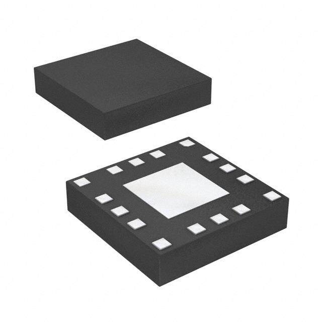
| 产品图片 |
|
| rohs | 符合RoHS无铅 / 符合限制有害物质指令(RoHS)规范要求 |
| 产品系列 | 接口 IC,RS-232接口集成电路,Analog Devices ADM3101EACPZ-250R7- |
| 数据手册 | |
| 产品型号 | ADM3101EACPZ-250R7 |
| PCN其它 | |
| 产品目录页面 | |
| 产品种类 | RS-232接口集成电路 |
| 供应商器件封装 | 12-LFCSP-VQ (3x3) |
| 关闭 | No |
| 其它名称 | ADM3101EACPZ-250R7DKR |
| 功能 | Transceiver |
| 包装 | Digi-Reel® |
| 协议 | RS232 |
| 双工 | 全 |
| 商标 | Analog Devices |
| 安装类型 | 表面贴装 |
| 安装风格 | SMD/SMT |
| 封装 | Reel |
| 封装/外壳 | 12-VFQFN 裸露焊盘,CSP |
| 封装/箱体 | LFCSP-12 |
| 工作温度 | -40°C ~ 85°C |
| 工作温度范围 | - 40 C to + 85 C |
| 工作电源电压 | 3 V to 5.5 V |
| 工厂包装数量 | 250 |
| 接收器滞后 | 400mV |
| 接收机数量 | 1 Receiver |
| 支持协议 | RS-232 |
| 数据速率 | 460Kbps |
| 最大工作温度 | + 85 C |
| 最小工作温度 | - 40 C |
| 标准包装 | 1 |
| 激励器数量 | 1 Driver |
| 电压-电源 | 3 V ~ 5.5 V |
| 电源电流 | 5 mA |
| 类型 | 收发器 |
| 系列 | ADM3101E |
| 驱动器/接收器数 | 1/1 |


- 商务部:美国ITC正式对集成电路等产品启动337调查
- 曝三星4nm工艺存在良率问题 高通将骁龙8 Gen1或转产台积电
- 太阳诱电将投资9.5亿元在常州建新厂生产MLCC 预计2023年完工
- 英特尔发布欧洲新工厂建设计划 深化IDM 2.0 战略
- 台积电先进制程称霸业界 有大客户加持明年业绩稳了
- 达到5530亿美元!SIA预计今年全球半导体销售额将创下新高
- 英特尔拟将自动驾驶子公司Mobileye上市 估值或超500亿美元
- 三星加码芯片和SET,合并消费电子和移动部门,撤换高东真等 CEO
- 三星电子宣布重大人事变动 还合并消费电子和移动部门
- 海关总署:前11个月进口集成电路产品价值2.52万亿元 增长14.8%


PDF Datasheet 数据手册内容提取
±15 kV ESD Protected, 3.3 V Single- Channel RS-232 Line Driver/Receiver Data Sheet ADM3101E FEATURES FUNCTIONAL BLOCK DIAGRAM 460 kbps data rate +3.3V INPUT 1 Tx and 1 Rx M0.1e eμtFs cEhIAa/rTgIeA p-2u3m2pE scpaepcaicfiitcoartsio ns 0.11C6µVF1+ CC11+– VO+L3T.A3VG ET OD O+6U.B6VLER VVCC+ +C06..313µVF +C0.51µF Contact discharge: ±8 kV 0.1CµF2+ C2+ +6.6V TO –6.6V V– C4 Air gap discharge: ±15 kV 16V C2– VOLTAGE INVERTER +01.61VµF APPLICATIONS CINMPOUST TIN T TOUT EOIUAT/TPIUAT-232E General-purpose RS-232 data links ADM3101E Industrial/telecommunications diagnostics ports CMOS ROUT R RIN EIA/TIA-232E OUTPUT INPUT* GND * RINETSEISRTNOARL 5OkNΩ T PHUEL RLS-D-2O3W2 NINPUT. 06766-001 Figure 1. GENERAL DESCRIPTION The ADM3101E is a high speed, single-channel, RS-232/ Because of the ±15 kV ESD protection of the ADM3101E ITU-T V.28 transceiver interface device that operates from input/output pins, this device is ideally suited for operation a single 3.3 V power supply. Low power consumption makes in electrically harsh environments or where RS-232 cables are it ideal for battery-powered portable instruments. frequently plugged and unplugged. The ADM3101E conforms to the EIA/TIA-232E and ITU-T V.28 Four external 0.1 μF charge pump capacitors are used for the specifications and operates at data rates of up to 460 kbps. voltage doubler/inverter permitting operation from a single 3.3 V supply. All RS-232 (T and R ) and CMOS (T and R ) inputs OUT IN IN OUT and outputs are protected against electrostatic discharges (up The ADM3101E is available in both a 12-lead LFCSP and 16-lead to ±15 kV ESD protection). QSOP, specified over the −40°C to +85°C temperature range. Rev. D Document Feedback Information furnished by Analog Devices is believed to be accurate and reliable. However, no responsibility is assumed by Analog Devices for its use, nor for any infringements of patents or other One Technology Way, P.O. Box 9106, Norwood, MA 02062-9106, U.S.A. rights of third parties that may result from its use. Specifications subject to change without notice. No license is granted by implication or otherwise under any patent or patent rights of Analog Devices. Tel: 781.329.4700 ©2007–2015 Analog Devices, Inc. All rights reserved. Trademarks and registered trademarks are the property of their respective owners. Technical Support www.analog.com
ADM3101E Data Sheet TABLE OF CONTENTS Features .............................................................................................. 1 Pin Configurations and Function Descriptions ............................5 Applications ....................................................................................... 1 Typical Performance Characteristics ..............................................6 Functional Block Diagram .............................................................. 1 Theory of Operation .........................................................................8 General Description ......................................................................... 1 Circuit Description .......................................................................8 Revision History ............................................................................... 2 High Baud Rate ..............................................................................8 Specifications ..................................................................................... 3 Outline Dimensions ..........................................................................9 Absolute Maximum Ratings ............................................................ 4 Ordering Guide .............................................................................9 ESD Caution .................................................................................. 4 REVISION HISTORY 5/15—Rev. C to Rev. D 10/07—Rev. 0 to Rev. A Change to θ , Thermal Impedance (LFCSP) Parameter, Changes to Figure 1 ........................................................................... 1 JA Table 2 ................................................................................................ 4 Changes to Table 1, RS-232 Receiver Section ................................ 3 Changes to Figure 2 and Table 3 ..................................................... 5 Changes to Table 3 ............................................................................. 5 Changes to Ordering Guide ............................................................ 9 Changes to Figure 11 ......................................................................... 8 Updated Outline Dimensions ......................................................... 9 5/07—Revision 0: Initial Version 7/08—Rev. B to Rev. C Changes to General Description Section ...................................... 1 Reformatted Table 1 ......................................................................... 4 Change to T Rating, Table 2 ......................................................... 4 IN Changes to Figure 2 .......................................................................... 5 Moved High Baud Rate Section ...................................................... 8 Added Exposed Pad Notation to Outline Dimensions ............... 9 12/07—Rev. A to Rev. B Added 16-Lead QSOP Package (Universal) ................................. 1 Updated Outline Dimensions ....................................................... 10 Changes to Ordering Guide .......................................................... 10 Rev. D | Page 2 of 12
Data Sheet ADM3101E SPECIFICATIONS V = 3.3 V ± 0.3 V, C1 to C4 = 0.1 μF, −40°C ≤ T ≤ +85°C, unless otherwise noted. CC A Table 1. Parameter Test Conditions/Comments Min Typ Max Unit DC CHARACTERISTICS Operating Voltage Range 3.0 3.3 5.5 V Power Supply Current, V No load 1.5 2.6 mA CC R = 3 kΩ to GND 5 7 mA L LOGIC Input Logic Threshold Low, V T 0.6 V INL IN Input Logic Threshold High, V T 1.4 V INH IN Input Logic Threshold Low, V T , V = 5.0 V ± 0.5 V 0.8 V INL IN CC Input Logic Threshold High, V T , V = 5.0 V ± 0.5 V 2.0 V INH IN CC CMOS Output Voltage Low, V I = 1.6 mA 0.4 V OL OUT CMOS Output Voltage High, VOH IOUT = −1 mA VCC − 0.6 V Logic Pull-Up Current T = GND to V 5 12 μA IN CC RS-232 RECEIVER EIA/TIA-232E Input Voltage Range1 −30 +30 V EIA/TIA-232E Input Threshold Low V = 3.0 V to 5.5 V 0.6 1.3 V CC EIA/TIA-232E Input Threshold High 1.6 2.4 V EIA/TIA-232E Input Hysteresis 0.4 V EIA/TIA-232E Input Resistance 3 5 7 kΩ TRANSMITTER Output Voltage Swing RS-232 V = 3.3 V to 5.5 V; transmitter output loaded ±5.0 ±5.7 V CC with 3 kΩ to ground RS-562 V = 3.0 V ±4.5 V CC Transmitter Output Resistance V = 0 V, V = ±2 V1 300 Ω CC OUT RS-232 Output Short-Circuit Current ±15 mA TIMING CHARACTERISTICS Maximum Data Rate V = 3.3 V, R = 3 kΩ to 7 kΩ, C = 50 pF to 1000 pF 460 kbps CC L L Receiver Propagation Delay t 0.4 μs PHL t 0.4 μs PLH Transmitter Propagation Delay R = 3 kΩ, C = 1000 pF 600 ns L L Transmitter Skew 80 ns Receiver Skew 70 ns Transition Region Slew Rate +3 V to −3 V or −3 V to +3 V, VCC = +3.3 V, 5.5 10 30 V/μs R = 3 kΩ, C = 1000 pF, T = 25°C1 L L A ESD PROTECTION RS-232 and CMOS I/O Pins Human body model air discharge ±15 kV Human body model contact discharge ±8 kV 1 Guaranteed by design. Rev. D | Page 3 of 12
ADM3101E Data Sheet ABSOLUTE MAXIMUM RATINGS T = 25°C, unless otherwise noted. Stresses at or above those listed under Absolute Maximum A Ratings may cause permanent damage to the product. This is a Table 2. stress rating only; functional operation of the product at these Parameter Rating or any other conditions above those indicated in the V −0.3 V to +6 V CC operational section of this specification is not implied. V+ (V − 0.3 V) to +13 V CC Operation beyond the maximum operating conditions for V− +0.3 V to −13 V extended periods may affect product reliability. Input Voltages T −0.3 V to (V + 0.3 V) ESD CAUTION IN CC R ±30 V IN Output Voltages T ±15 V OUT R −0.3 V to (V + 0.3 V) OUT CC Short-Circuit Duration T Continuous OUT Package Information θ , Thermal Impedance (LFCSP) 80°C/W JA θ , Thermal Impedance (QSOP) 149.97°C/W JA Operating Temperature Range Industrial (A Version) −40°C to +85°C Storage Temperature Range −65°C to +150°C Pb-Free Temperature (Soldering, 10 sec) 260°C Rev. D | Page 4 of 12
Data Sheet ADM3101E PIN CONFIGURATIONS AND FUNCTION DESCRIPTIONS – + – 1 2 2 C C C C1– 1 16 C2+ 21 11 01 C1+ 2 15 C2– C1+1 9RIN NC 3 14 NC ADM3101E ADM3101E ROUT 2 TOP VIEW 8TOUT ROUT 4 TOP VIEW 13 RIN (Not to Scale) TIN 5 (Not to Scale) 12 TOUT TIN3 7V– NC 6 11 NC 4 5 6 V+ 7 10 V– N1 . O ETTXHEPISSO CSOEDN NPEACDT. ITOHNE I SE XNPOOTS RE+VEDQ PUAVICCRDE MDDNGU TSOT MBEEE CTO ENLNEECCTTREICDA TLO P GENRDF.ORMANCE. 06766-002 VCC 8NC = NO CONNECT9 GND 06766-014 Figure 2. LFCSP Pin Configuration Figure 3. QSOP Pin Configuration Table 3. Pin Function Descriptions Pin No.1 LFCSP QSOP Mnemonic Description 1, 12 2, 1 C1+, C1− Positive and Negative Connections for Charge Pump Capacitor. External Capacitor C1 is connected between these pins; a 0.1 μF capacitor is recommended, but larger capacitors up to 10 μF can be used. 2 4 R Receiver Output. This pin outputs CMOS output logic levels. OUT 3 5 T Transmitter (Driver) Input. This input accepts TTL/CMOS levels. IN 4 7 V+ Internally Generated Positive Supply (+6 V Nominal). 5 8 V Power Supply Input, 3.0 V to 5.5 V. CC 6 9 GND Ground. Must be connected to 0 V. 7 10 V– Internally Generated Negative Supply (−6 V Nominal). 8 12 T Transmitter (Driver) Output. This pin outputs RS-232 signal levels (typically ±6 V). OUT 9 13 R Receiver Input. This input accepts RS-232 signal levels. An internal 5 kΩ pull-down resistor to GND is IN connected on the input. 10, 11 15, 16 C2−, C2+ Positive and Negative Connections for Charge Pump Capacitor. External Capacitor C2 is connected between these pins; a 0.1 μF capacitor is recommended, but larger capacitors up to 10 μF can be used. N/A 3, 6, 11, 14 NC No Connect. These pins should always remain unconnected. EPAD N/A EPAD Exposed Pad. The exposed pad must be connected to GND. This connection is not required to meet electrical performance. 1 N/A means not applicable. Rev. D | Page 5 of 12
ADM3101E Data Sheet TYPICAL PERFORMANCE CHARACTERISTICS 8 8 VCC = 3.3V VCC = 3.3V 6 6 Tx OUTPUT HIGH V+ 4 4 TPUT (V) 20 AGE (V) 20 U T Tx O –2 VOL –2 –4 –4 Tx OUTPUT LOW V– –6 –6 –8 –8 0 200 LOAD4 0C0APACITAN6C00E (pF) 800 1000 06766-003 0 1 LOAD CUR2RENT (mA) 3 4 06766-006 Figure 4. Transmitter Output Voltage High/Low vs. Figure 7. Charge Pump V+, V− vs. Load Current Load Capacitance @ 460 kbps 15 350 300 10 Tx OUTPUT HIGH Ω) V– CE ( 250 5 N V) DA Tx OUTPUT ( –50 E PUMP IMPE 210500 V+ G R 100 A Tx OUTPUT LOW H C –10 50 –15 0 3 4 VCC (V) 5 6 06766-004 3 4 VCC (V) 5 6 06766-007 Figure 5. Transmitter Output Voltage High/Low vs. VCC, RL = 3 kΩ Figure 8. Charge Pump Impedance vs. VCC 8 14 VCC = 3.3V VCC = 3.3V 6 12 Tx OUTPUT HIGH 4 10 V) 2 UTPUT ( 0 (mA)D 8 Tx O –2 ID 6 4 –4 Tx OUTPUT LOW –6 2 –8 0 0 1 LOAD CUR2RENT (mA) 3 4 06766-005 0 200 LOAD4 0C0APACITAN6C00E (pF) 800 1000 06766-008 Figure 6. Transmitter Output Voltage High/Low vs. Load Current Figure 9. Power Supply Current vs. Load Capacitance Rev. D | Page 6 of 12
Data Sheet ADM3101E 5.0 4.5 V V) 4.0 5V/DI 1 LDS ( 3.5 O SH 3.0 E R H 2.5 T E 5V/DIV 2 OLTAG 21..05 V N TI 1.0 VCC = 3.3V 0.5 LOAD = 3kΩ AND 1nFTIME (1µs/DIV) 06766-009 03.0 3.5 4.0 VCC (V) 4.5 5.0 5.5 06766-010 Figure 10. 460 kbps Data Transmission Figure 11. TIN Voltage Threshold vs. VCC Rev. D | Page 7 of 12
ADM3101E Data Sheet THEORY OF OPERATION The ADM3101E is a single-channel RS-232 line driver/receiver. S1 S3 V+ GND Step-up voltage converters, coupled with level shifting trans- FROM + + VOLTAGE C2 C4 mitters and receivers, allow RS-232 levels to be developed while DOUBLER S2 S4 GND V– = –(V+) operating from a single 3.3 V supply. CanM aObsSo tluecteh nmoilnoigmyu ism u, saeldlo twoi nkege mp athxeim puomwe br adtitsesriyp alitfieo nin t o OISNCTIELRLANTAOLR 06766-013 Figure 14. Charge Pump Voltage Inverter portable applications. 3.3 V Logic to EIA/TIA-232E Transmitter CIRCUIT DESCRIPTION The transmitter driver converts the 3.3 V logic input levels The internal circuitry consists of the following main sections: into RS-232 output levels. When driving an RS-232 load with A charge pump voltage converter VCC = 3.3 V, the output voltage swing is typically ±6 V. Internally, the T pin has a weak pull-up that allows it to be driven by an A 3.3 V logic to an EIA/TIA-232E transmitter IN open-drain output, but the maximum operating data rate is An EIA/TIA-232E to a 3.3 V logic receiver reduced when the T pin is driven by an open-drain pin. IN +3.3V INPUT EIA/TIA-232E to 3.3 V Logic Receiver 0.11C6µVF1+ CC11+– VO+L3T.A3VG ET OD O+6U.B6VLER VVCC+ +C06..313µVF +C0.51µF Tinhpeu rt elceevievle arn ids atrna innsvlaetretsin itg ilnetvoe la s 3h.i3f tVer ltohgaitc aocuctepputst ltehvee Rl. ST-h2e3 2 input has an internal 5 kΩ pull-down resistor to ground and is 0.1CµF2+ C2+ +6.6V TO –6.6V V– C4 protected against overvoltages of up to ±30 V. An unconnected 16V C2– VOLTAGE INVERTER +01.61VµF input is pulled to 0 V by the internal 5 kΩ pull-down resistor, CINMPOUST TIN T TOUT EOIUAT/TPIUAT-232E wnehcitcehd, itnhperuetf oorre f,o rre asunl tisn pinu ta cLoongnice c1t eodu ttop uGt NleDve. l for an uncon- ADM3101E The receiver has a Schmitt trigger input with a hysteresis level OUCTMPOUST ROUT R RIN EINIAP/UTTIA*-232E of 0.4 V, which ensures error-free reception for both a noisy input and for an input with slow transition times. GND CMOS Input Voltage Thresholds * RINETSEISRTNOARL 5OkNΩ T PHUEL RLS-D-2O3W2 NINPUT. 06766-011 AThDeM C3M10O1SE ianrpeu dt easnigdn oeudt ptou ti nptienrsf a(cTeI Nw ainthd 1R.8O UVT) l oogf itch e Figure 12. Typical Operating Circuit thresholds when V = 3.3 V. CC Charge Pump Voltage Converter The CMOS input and output pins (T and R ) of the IN OUT The charge pump voltage converter consists of a 200 kHz oscil- ADM3101E are also designed to interface with TTL/CMOS lator and a switching matrix. The converter generates a ±6.6 V logic thresholds when V = 5 V. CC supply (when unloaded) from the 3.3 V input level. This is achieved ESD Protection on RS-232 and CMOS I/O Pins in two stages by using a switched capacitor technique, as illustrated in Figure 13 and Figure 14. First, the 3.3 V input supply is doubled All RS-232 (TOUT and RIN) and CMOS (TIN and ROUT) inputs to +6.6 V by using C1 as the charge storage element. The +6.6 V and outputs are protected against electrostatic discharges (up level is then inverted to generate −6.6 V using C2 as the storage to ±15 kV). element. C3 is shown connected between V+ and VCC but is HIGH BAUD RATE equally effective if connected between V+ and GND. The ADM3101E features high slew rates, permitting data trans- The C3 and C4 capacitors are used to reduce the output ripple. mission at rates well in excess of the EIA/RS-232 specifications. The values are not critical and can be increased, if desired. Larger The RS-232 voltage levels are maintained at data rates of up to capacitors (up to 10 μF) can also be used in place of the C1, C2, 460 kbps, even under worst-case loading conditions, when T is IN C3, and C4 capacitors. driven by a push-pull output. The slew rate is internally controlled S1 S3 to less than 30 V/μs to minimize EMI interference. VCC V+ = 2VCC + + C1 C3 S2 S4 GND VCC OISNCTIELRLANTAOLR 06766-012 Figure 13. Charge Pump Voltage Doubler Rev. D | Page 8 of 12
Data Sheet ADM3101E OUTLINE DIMENSIONS 3.10 0.30 3.00 SQ 0.23 PIN 1 2.90 0.18 INDICATOR PIN 1 0.50 10 12 INDICATOR BSC 9 1 EXPOSED 1.45 PAD 1.30 SQ 1.15 7 3 0.70 6 4 0.25 MIN TOP VIEW 0.60 BOTTOM VIEW 0.50 0.80 FOR PROPER CONNECTION OF 0.75 THE EXPOSED PAD, REFER TO 0.05 MAX THE PIN CONFIGURATION AND 0.70 0.02 NOM FUNCTION DESCRIPTIONS SECTION OF THIS DATA SHEET. COPLANARITY SEATING 0.08 PLANE 0.20 REF COMPLIANTTOJEDEC STANDARDS MO-220-WEED. 111808-A Figure 15. 12-Lead Lead Frame Chip Scale Package [LFCSP_WQ] 3 mm × 3 mm Body, Very Very Thin Quad (CP-12-4) Dimensions shown in millimeters 0.197 (5.00) 0.193 (4.90) 0.189 (4.80) 16 9 0.158 (4.01) 0.154 (3.91) 0.150 (3.81) 0.244 (6.20) 1 8 0.236 (5.99) 0.228 (5.79) 0.010 (0.25) 0.020 (0.51) 0.065 (1.65) 0.069 (1.75) 0.006 (0.15) 0.010 (0.25) 0.049 (1.25) 0.053 (1.35) 0.010 (0.25) CO0P.0L0A4 N(0A.1R0I)TY 0.02B5S (C0.64) 0.012 (0.30) SPELAATNIENG 80°° 0.050 (1.27) 0R.E04F1 (1.04) 0.004 (0.10) 0.016 (0.41) 0.008 (0.20) COMPLIANTTO JEDEC STANDARDS MO-137-AB C(RINOEFNPETARRREOENNLCLTEIHN EOGSN EDLSIYM)AEANNRDSEI AORRNOESU NANORDEET DAIN-PO IPFNRFCO HINPECRSHI;A METEQIL UFLIOIVMRAE LUTEESNRET DISNI M FDOEERNSSIGIONN.S 09-12-2014-A Figure 16. 16-Lead Shrink Small Outline Package [QSOP] (RQ-16) Dimensions shown in inches and (millimeters) ORDERING GUIDE Model1 Temperature Range Package Description Package Option Branding ADM3101EACPZ-REEL −40°C to +85°C 12-Lead Lead Frame Chip Scale Package [LFCSP_WQ] CP-12-4 MA6 ADM3101EACPZ-250R7 –40°C to +85°C 12-Lead Lead Frame Chip Scale Package [LFCSP_WQ] CP-12-4 MA6 ADM3101EARQZ –40°C to +85°C 16-Lead Shrink Small Outline Package [QSOP] RQ-16 ADM3101EARQZ-REEL –40°C to +85°C 16-Lead Shrink Small Outline Package [QSOP] RQ-16 1 Z = RoHS Compliant Part. Rev. D | Page 9 of 12
ADM3101E Data Sheet NOTES Rev. D | Page 10 of 12
Data Sheet ADM3101E NOTES Rev. D | Page 11 of 12
ADM3101E Data Sheet NOTES ©2007–2015 Analog Devices, Inc. All rights reserved. Trademarks and registered trademarks are the property of their respective owners. D06766-0-5/15(D) Rev. D | Page 12 of 12
Mouser Electronics Authorized Distributor Click to View Pricing, Inventory, Delivery & Lifecycle Information: A nalog Devices Inc.: ADM3101EARQZ-REEL ADM3101EACPZ-REEL ADM3101EARQZ ADM3101EACPZ-250R7