ICGOO在线商城 > 集成电路(IC) > 接口 - 驱动器,接收器,收发器 > SN65C3221EPWR
 Datasheet下载
- 型号: SN65C3221EPWR
- 制造商: Texas Instruments
- 库位|库存: xxxx|xxxx
- 要求:
| 数量阶梯 | 香港交货 | 国内含税 |
| +xxxx | $xxxx | ¥xxxx |
查看当月历史价格
查看今年历史价格
SN65C3221EPWR产品简介:
ICGOO电子元器件商城为您提供SN65C3221EPWR由Texas Instruments设计生产,在icgoo商城现货销售,并且可以通过原厂、代理商等渠道进行代购。 SN65C3221EPWR价格参考。Texas InstrumentsSN65C3221EPWR封装/规格:接口 - 驱动器,接收器,收发器, 1/1 Transceiver Full RS232 16-TSSOP。您可以下载SN65C3221EPWR参考资料、Datasheet数据手册功能说明书,资料中有SN65C3221EPWR 详细功能的应用电路图电压和使用方法及教程。
SN65C3221EPWR是德州仪器(Texas Instruments)生产的一款RS-232接口收发器,属于接口驱动器、接收器、收发器类别。该芯片集成了单通道RS-232收发器,支持从单一3.3V电源产生符合RS-232标准的电压信号,具备低功耗、高集成度和高可靠性等特点。

其主要应用场景包括工业控制设备、嵌入式系统、通信模块、医疗仪器、测试测量设备以及需要串行通信功能的便携式设备。由于其采用小尺寸TSSOP封装(PWR),适用于空间受限的电路板设计。该器件广泛用于微控制器与PC或其他外设之间的异步串行数据传输,例如在工控人机界面、条码扫描器、POS终端和远程监控系统中实现稳定可靠的通信连接。

此外,SN65C3221EPWR内置电荷泵,可生成±8V至±15V的RS-232电平,确保在噪声环境下仍能可靠通信,并具备过温保护和短路保护功能,适合工业级温度范围(-40°C 至 +85°C)应用,因此在要求高稳定性和耐用性的工业环境中尤为适用。
| 参数 | 数值 |
| 产品目录 | 集成电路 (IC)半导体 |
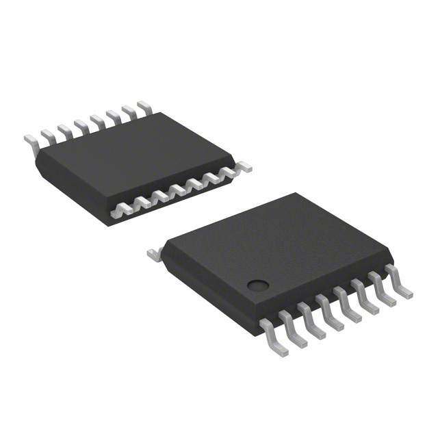
| 描述 | IC LINE DVR/RCVR 1CH 16-TSSOPRS-232接口集成电路 RS-232 1 Mbit/s Line Driver/Receiver |
| Duplex | Full Duplex |
| 产品分类 | |
| 品牌 | Texas Instruments |
| 产品手册 | |
| 产品图片 |
|
| rohs | 符合RoHS无铅 / 符合限制有害物质指令(RoHS)规范要求 |
| 产品系列 | 接口 IC,RS-232接口集成电路,Texas Instruments SN65C3221EPWR- |
| 数据手册 | |
| 产品型号 | SN65C3221EPWR |
| 产品目录页面 | |
| 产品种类 | RS-232接口集成电路 |
| 传播延迟时间ns | 0.15 us |
| 供应商器件封装 | 16-TSSOP |
| 关闭 | Yes |
| 其它名称 | 296-20992-2 |
| 功能 | Transceiver |
| 包装 | 带卷 (TR) |
| 协议 | RS232 |
| 单位重量 | 62 mg |
| 双工 | 全 |
| 商标 | Texas Instruments |
| 安装类型 | 表面贴装 |
| 安装风格 | SMD/SMT |
| 封装 | Reel |
| 封装/外壳 | 16-TSSOP(0.173",4.40mm 宽) |
| 封装/箱体 | TSSOP-16 |
| 工作温度 | -40°C ~ 85°C |
| 工作温度范围 | - 40 C to + 85 C |
| 工作电源电压 | 3.3 V, 5 V |
| 工厂包装数量 | 2000 |
| 接收器滞后 | 500mV |
| 接收机数量 | 1 Receiver |
| 数据速率 | 1Mbps |
| 最大工作温度 | + 85 C |
| 最小工作温度 | - 40 C |
| 标准包装 | 2,000 |
| 激励器数量 | 1 Driver |
| 电压-电源 | 3 V ~ 5.5 V |
| 电源电流 | 1 mA |
| 类型 | 收发器 |
| 系列 | SN65C3221E |
| 输入/输出端数量 | 4 |
| 驱动器/接收器数 | 1/1 |


- 商务部:美国ITC正式对集成电路等产品启动337调查
- 曝三星4nm工艺存在良率问题 高通将骁龙8 Gen1或转产台积电
- 太阳诱电将投资9.5亿元在常州建新厂生产MLCC 预计2023年完工
- 英特尔发布欧洲新工厂建设计划 深化IDM 2.0 战略
- 台积电先进制程称霸业界 有大客户加持明年业绩稳了
- 达到5530亿美元!SIA预计今年全球半导体销售额将创下新高
- 英特尔拟将自动驾驶子公司Mobileye上市 估值或超500亿美元
- 三星加码芯片和SET,合并消费电子和移动部门,撤换高东真等 CEO
- 三星电子宣布重大人事变动 还合并消费电子和移动部门
- 海关总署:前11个月进口集成电路产品价值2.52万亿元 增长14.8%


PDF Datasheet 数据手册内容提取
SN65C3221E,, SN75C3221E www.ti.com.................................................................................................................................................. SLLS694B–NOVEMBER2005–REVISEDAPRIL2009 3-V TO 5.5-V SINGLE-CHANNEL RS-232 1-Mbit/s LINE DRIVER/RECEIVER WITH ±15-kV IEC ESD PROTECTION FEATURES 1 DB OR PW PACKAGE • ESDProtectionforRS-232Pins (TOP VIEW) – ±15-kVHuman-BodyModel(HBM) – ±8-kVIEC61000-4-2ContactDischarge EN 1 16 FORCEOFF – ±15-kVIEC61000-4-2Air-GapDischarge C1+ 2 15 VCC V+ 3 14 GND • OperateWith3-Vto5.5-VV Supply CC C1− 4 13 DOUT • Operateupto1Mbit/s C2+ 5 12 FORCEON • LowStandbyCurrent...1m ATyp C2− 6 11 DIN • ExternalCapacitors...4×0.1m F V− 7 10 INVALID • Accepts5-VLogicInputWith3.3-VSupply RIN 8 9 ROUT • RS-232Bus-PinESDProtectionExceeds±15 kVUsingHuman-BodyModel(HBM) • Auto-PowerdownFeatureAutomatically DisablesDriversforPowerSavings APPLICATIONS • Battery-Powered,Hand-Held,andPortable Equipment • PDAsandPalmtopPCs • Notebooks,Sub-Notebooks,andLaptops • DigitalCameras • MobilePhonesandWirelessDevices DESCRIPTION/ORDERING INFORMATION The SN65C3221E and SN75C3221E consist of one line driver, one line receiver, and a dual charge-pump circuit with ±15-kV IEC ESD protection pin to pin (serial-port connection pins, including GND). These devices provide the electrical interface between an asynchronous communication controller and the serial-port connector. The charge pump and four small external capacitors allow operation from a single 3-V to 5.5-V supply. These devices operateatdatasignalingratesupto1Mbit/sandadriveroutputslewrateof24V/m sto150V/m s. Flexible control options for power management are available when the serial port is inactive. The auto-powerdown feature functions when FORCEON is low and FORCEOFF is high. During this mode of operation, if the devices do not sense a valid RS-232 signal on the receiver input, the driver output is disabled. If FORCEOFF is set low and EN is high, both the driver and receiver are shut off, and the supply current is reduced to 1 m A. Disconnecting the serial port or turning off the peripheral drivers causes the auto-powerdown condition to occur. Auto-powerdown can be disabled when FORCEON and FORCEOFF are high. With auto-powerdown enabled, the device is activated automatically when a valid signal is applied to the receiver input. The INVALID output notifies the user if an RS-232 signal is present at the receiver input. INVALID is high (valid data) if the receiver input voltage is greater than 2.7 V or less than –2.7 V, or has been between –0.3 V and 0.3 V for less than 30 m s. INVALID is low (invalid data) if the receiver input voltage is between –0.3 V and 0.3Vformorethan30m s.SeeFigure5forreceiverinputlevels. 1 Pleasebeawarethatanimportantnoticeconcerningavailability,standardwarranty,anduseincriticalapplicationsofTexas Instrumentssemiconductorproductsanddisclaimerstheretoappearsattheendofthisdatasheet. PRODUCTIONDATAinformationiscurrentasofpublicationdate. Copyright©2005–2009,TexasInstrumentsIncorporated Products conform to specifications per the terms of the Texas Instruments standard warranty. Production processing does not necessarilyincludetestingofallparameters.
SN65C3221E,, SN75C3221E SLLS694B–NOVEMBER2005–REVISEDAPRIL2009.................................................................................................................................................. www.ti.com ORDERINGINFORMATION T PACKAGE(1)(2) ORDERABLEPARTNUMBER TOP-SIDEMARKING A SSOP–DB Reelof2000 SN75C3221EDBR MY221E –0°Cto70°C Tubeof90 SN75C3221EPW TSSOP–PW MY221E Reelof2000 SN75C3221EPWR SSOP–DB Reelof2000 SN65C3221EDBR MU221E –40°Cto85°C Tubeof90 SN65C3221EPW TSSOP–PW MU221E Reelof2000 SN65C3221EPWR (1) Packagedrawings,standardpackingquantities,thermaldata,symbolization,andPCBdesignguidelinesareavailableat www.ti.com/sc/package. (2) Forthemostcurrentpackageandorderinginformation,seethePackageOptionAddendumattheendofthisdocument,orseetheTI websiteatwww.ti.com. FUNCTIONTABLES abc EACHDRIVER(1) INPUTS OUTPUT DIN FORCEON FORCEOFF VALIDRIN DOUT DRIVERSTATUS RS-232LEVEL X X L X Z Poweredoff L H H X H Normaloperationwith H H H X L auto-powerdowndisabled L L H Yes H Normaloperationwith H L H Yes L auto-powerdownenabled L L H No Z Poweredoffby H L H No Z auto-powerdownfeature (1) H=highlevel,L=lowlevel,X=irrelevant,Z=highimpedance abc EACHRECEIVER(1) INPUTS OUTPUT RIN EN VALIDRIN ROUT RS-232LEVEL L L X H H L X L X H X Z Open L No H (1) H=highlevel,L=lowlevel,X=irrelevant,Z=highimpedance(off), Open=disconnectedinputorconnecteddriveroff 2 SubmitDocumentationFeedback Copyright©2005–2009,TexasInstrumentsIncorporated ProductFolderLink(s):SN65C3221ESN75C3221E
SN65C3221E,, SN75C3221E www.ti.com.................................................................................................................................................. SLLS694B–NOVEMBER2005–REVISEDAPRIL2009 LOGICDIAGRAM(POSITIVELOGIC) 11 13 DIN DOUT 16 FORCEOFF 10 Auto-powerdown INVALID 12 FORCEON 9 8 ROUT RIN 1 EN Copyright©2005–2009,TexasInstrumentsIncorporated SubmitDocumentationFeedback 3 ProductFolderLink(s):SN65C3221ESN75C3221E
SN65C3221E,, SN75C3221E SLLS694B–NOVEMBER2005–REVISEDAPRIL2009.................................................................................................................................................. www.ti.com Table1.1-Mbit/sRS-232Parts SUPPLY PART TEMPERATURE DRIVER RECEIVER ESD V FEATURE PIN/PACKAGE NO. RANGE NO. NO. CC (V) ±15-kVAir-Gap, 16-pinSOIC, SN65C3221E 1 1 ±8-kVContact, 3.3or5 Autopowerdown SSOP,TSSOP ±15-kVHBM ±15-kVAir-Gap, 16-pinSOIC, SN65C3232E 2 2 ±8-kVContact, 3.3or5 Lowpincount SSOP,TSSOP ±15-kVHBM ±8-kVAir-Gap, Autopowerdownplus, MAX3227I 1 1 ±8-kVContact, 3.3or5 16-pinSSOP readysignal ±15-kVHBM 16-pinSOIC, SN65C3221 1 1 ±15-kVHBM 3.3or5 Autopowerdown SSOP,TSSOP –40°Cto85°C Autopowerdown, 20-pinSOIC, SN65C3223 2 2 ±15-kVHBM 3.3or5 enablesignal SSOP,TSSOP Enable, 20-pinSOIC, SN65C3222 2 2 ±15-kVHBM 3.3or5 powerdownsignal SSOP,TSSOP 16-pinSOIC, SN65C3232 2 2 ±15-kVHBM 3.3or5 Lowpincount SSOP,TSSOP 28-pinSOIC, SN65C3238 5 3 ±15-kVHBM 3.3or5 Autopowerdownplus SSOP,TSSOP 28-pinSOIC, SN65C3243 3 5 ±15-kVHBM 3.3or5 Autopowerdown SSOP,TSSOP ±15-kVAir-Gap, 16-pinSOIC, SN75C3221E 1 1 ±8-kVContact, 3.3or5 Autopowerdown SSOP,TSSOP ±15-kVHBM ±15-kVAir-Gap, 16-pinSOIC, SN75C3232E 2 2 ±8-kVContact, 3.3or5 Lowpincount SSOP,TSSOP ±15-kVHBM ±8-kVAir-Gap, Autopowerdownplus, MAX3227C 1 1 ±8-kVContact, 3.3or5 16-pinSSOP readysignal ±15-kVHBM 16-pinSOIC, SN75C3221 1 1 ±15-kVHBM 3.3or5 Autopowerdown SSOP,TSSOP 0°Cto70°C Autopowerdown, 20-pinSOIC, SN75C3223 2 2 ±15-kVHBM 3.5or5 enablesignal SSOP,TSSOP Enable, 20-pinSOIC, SN75C3222 2 2 ±15-kVHBM 3.3or5 powerdownsignal SSOP,TSSOP 16-pinSOIC, SN75C3232 2 2 ±15-kVHBM 3.3or5 Lowpincount SSOP,TSSOP 28-pinSOIC, SN75C3238 5 3 ±15-kVHBM 3.3or5 Autopowerdownplus SSOP,TSSOP 28-pinSOIC, SN75C3243 3 5 ±15-kVHBM 3.3or5 Autopowerdown SSOP,TSSOP 4 SubmitDocumentationFeedback Copyright©2005–2009,TexasInstrumentsIncorporated ProductFolderLink(s):SN65C3221ESN75C3221E
SN65C3221E,, SN75C3221E www.ti.com.................................................................................................................................................. SLLS694B–NOVEMBER2005–REVISEDAPRIL2009 Absolute Maximum Ratings(1) overoperatingfree-airtemperaturerange(unlessotherwisenoted) MIN MAX UNIT V Supplyvoltagerange(2) –0.3 6 V CC V+ Positiveoutputsupplyvoltagerange(2) –0.3 7 V V– Negativeoutputsupplyvoltagerange(2) 0.3 –7 V V+–V– Supplyvoltagedifference(2) 13 V Driver(FORCEOFF,FORCEON,EN) –0.3 6 V Inputvoltagerange V I Receiver –25 25 Driver –13.2 13.2 V Outputvoltagerange V O Receiver(INVALID) –0.3 V +0.3 CC DBpackage 82 q Packagethermalimpedance(3)(4) °C/W JA PWpackage 108 T Operatingvirtualjunctiontemperature 150 °C J T Storagetemperaturerange –65 150 °C stg (1) Stressesbeyondthoselistedunder"absolutemaximumratings"maycausepermanentdamagetothedevice.Thesearestressratings only,andfunctionaloperationofthedeviceattheseoranyotherconditionsbeyondthoseindicatedunder"recommendedoperating conditions"isnotimplied.Exposuretoabsolute-maximum-ratedconditionsforextendedperiodsmayaffectdevicereliability. (2) AllvoltagesarewithrespecttonetworkGND. (3) MaximumpowerdissipationisafunctionofT(max),q ,andT .Themaximumallowablepowerdissipationatanyallowableambient J JA A temperatureisP =(T(max)–T )/q .OperatingattheabsolutemaximumT of150°Ccanaffectreliability. D J A JA J (4) ThepackagethermalimpedanceiscalculatedinaccordancewithJESD51-7. Recommended Operating Conditions(1) SeeFigure6 MIN NOM MAX UNIT V =3.3V 3 3.3 3.6 CC Supplyvoltage V V =5V 4.5 5 5.5 CC Driverandcontrol VCC=3.3V 2 V DIN,FORCEOFF,FORCEON,EN V IH high-levelinputvoltage V =5V 2.4 CC Driverandcontrol V DIN,FORCEOFF,FORCEON,EN 0.8 V IL low-levelinputvoltage V Driverandcontrolinputvoltage DIN,FORCEOFF,FORCEON 0 5.5 V I V Receiverinputvoltage –25 25 V I SN65C3221E –40 85 T Operatingfree-airtemperature °C A SN75C3221E 0 70 (1) TestconditionsareC1–C4=0.1m FatV =3.3V±0.3V;C1=0.047m F,C2–C4=0.33m FatV =5V±0.5V. CC CC Electrical Characteristics(1) overrecommendedrangesofsupplyvoltageandoperatingfree-airtemperature(unlessotherwisenoted)(seeFigure6) PARAMETER TESTCONDITIONS MIN TYP(2) MAX UNIT I Inputleakagecurrent FORCEOFF,FORCEON,EN ±0.01 ±1 m A I Noload, Auto-powerdowndisabled 0.3 1 mA FORCEOFFandFORCEONatV CC Supplycurrent Poweredoff Noload,FORCEOFFatGND 1 10 I CC (T =25°C) A Noload,FORCEOFFatVCC, m A Auto-powerdownenabled FORCEONatGND, 1 10 AllRINareopenorgrounded (1) TestconditionsareC1–C4=0.1m FatV =3.3V±0.3V;C1=0.047m F,C2–C4=0.33m FatV =5V±0.5V. CC CC (2) AlltypicalvaluesareatV =3.3VorV =5V,andT =25°C. CC CC A Copyright©2005–2009,TexasInstrumentsIncorporated SubmitDocumentationFeedback 5 ProductFolderLink(s):SN65C3221ESN75C3221E
SN65C3221E,, SN75C3221E SLLS694B–NOVEMBER2005–REVISEDAPRIL2009.................................................................................................................................................. www.ti.com DRIVER SECTION abc Electrical Characteristics(1) overrecommendedrangesofsupplyvoltageandoperatingfree-airtemperature(unlessotherwisenoted)(seeFigure6) PARAMETER TESTCONDITIONS MIN TYP(2) MAX UNIT V High-leveloutputvoltage DOUTatR =3kΩtoGND, DIN=GND 5 5.4 V OH L V Low-leveloutputvoltage DOUTatR =3kΩtoGND, DIN=V –5 –5.4 V OL L CC I High-levelinputcurrent V =V ±0.01 ±1 m A IH I CC I Low-levelinputcurrent V atGND ±0.01 ±1 m A IL I Short-circuitoutput VCC=3.6V, VO=0V ±35 ±60 IOS current(3) V =5.5V, V =0V ±35 ±90 mA CC O r Outputresistance V ,V+,andV–=0V, V =±2V 300 10M Ω o CC O V =±12V, V =3Vto3.6V ±25 I Outputleakagecurrent FORCEOFF=GND O CC m A off V =±10V, V =4.5Vto5.5V ±25 O CC (1) TestconditionsareC1–C4=0.1m FatV =3.3V±0.3V;C1=0.047m F,C2–C4=0.33m FatV =5V±0.5V. CC CC (2) AlltypicalvaluesareatV =3.3VorV =5V,andT =25°C. CC CC A (3) Short-circuitdurationsshouldbecontrolledtopreventexceedingthedeviceabsolutepower-dissipationratings,andnotmorethanone outputshouldbeshortedatatime. Switching Characteristics(1) overrecommendedrangesofsupplyvoltageandoperatingfree-airtemperature(unlessotherwisenoted)(seeFigure6) PARAMETER TESTCONDITIONS MIN TYP(2) MAX UNIT C =1000pF 250 L Maximumdatarate R =3kΩ C =250pF, V =3Vto4.5V 1000 kbit/s (seeFigure1) L L CC C =1000pF, V =4.5Vto5.5V 1000 L CC t Pulseskew(3) C =150pFto2500pF, R =3kΩto7kΩ, SeeFigure2 100 ns sk(p) L L Slewrate, SR(tr) transitionregion V =3.3V, R =3kΩto7kΩ, C =150pFto1000pF 18 150 V/m s CC L L (seeFigure1) (1) TestconditionsareC1–C4=0.1m FatV =3.3V±0.3V;C1=0.047m F,C2–C4=0.33m FatV =5V±0.5V. CC CC (2) AlltypicalvaluesareatV =3.3VorV =5V,andT =25°C. CC CC A (3) Pulseskewisdefinedas|t -t |ofeachchannelofthesamedevice. PLH PHL ESD Protection TERMINAL TESTCONDITIONS TYP UNIT NAME NO. HBM ±15 DOUT 13 IEC61000-4-2ContactDischarge ±8 kV IEC61000-4-2Air-GapDischarge ±15 6 SubmitDocumentationFeedback Copyright©2005–2009,TexasInstrumentsIncorporated ProductFolderLink(s):SN65C3221ESN75C3221E
SN65C3221E,, SN75C3221E www.ti.com.................................................................................................................................................. SLLS694B–NOVEMBER2005–REVISEDAPRIL2009 RECEIVER SECTION abc Electrical Characteristics(1) overrecommendedrangesofsupplyvoltageandoperatingfree-airtemperature(unlessotherwisenoted)(seeFigure6) PARAMETER TESTCONDITIONS MIN TYP(2) MAX UNIT V High-leveloutputvoltage I =–1mA V –0.6V V –0.1V V OH OH CC CC V Low-leveloutputvoltage I =1.6mA 0.4 V OL OL V =3.3V 1.6 2.4 CC V Positive-goinginputthresholdvoltage V IT+ V =5V 1.9 2.4 CC V =3.3V 0.6 1.1 CC V Negative-goinginputthresholdvoltage V IT– V =5V 0.8 1.4 CC V Inputhysteresis(V –V ) 0.5 V hys IT+ IT– I Outputleakagecurrent FORCEOFF=0V ±0.05 ±10 m A off r Inputresistance V =±3Vto±25V 3 5 7 kΩ i I (1) TestconditionsareC1–C4=0.1m FatV =3.3V±0.3V;C1=0.047m F,C2–C4=0.33m FatV =5V±0.5V. CC CC (2) AlltypicalvaluesareatV =3.3VorV =5V,andT =25°C. CC CC A Switching Characteristics(1) overrecommendedrangesofsupplyvoltageandoperatingfree-airtemperature(unlessotherwisenoted)(seeFigure6) PARAMETER TESTCONDITIONS TYP(2) UNIT t Propagationdelaytime,low-tohigh-leveloutput C =150pF,SeeFigure3 150 ns PLH L t Propagationdelaytime,high-tolow-leveloutput C =150pF,SeeFigure3 150 ns PHL L t Outputenabletime C =150pF,R =3kΩ,SeeFigure4 200 ns en L L t Outputdisabletime C =150pF,R =3kΩ,SeeFigure4 200 ns dis L L t Pulseskew(3) SeeFigure3 50 ns sk(p) (1) TestconditionsareC1–C4=0.1m FatV =3.3V±0.3V;C1=0.047m F,C2–C4=0.33m FatV =5V±0.5V. CC CC (2) AlltypicalvaluesareatV =3.3VorV =5V,andT =25°C. CC CC A (3) Pulseskewisdefinedas|t -t |ofeachchannelofthesamedevice. PLH PHL ESD Protection TERMINAL TESTCONDITIONS TYP UNIT NAME NO. HBM ±15 RIN 8 IEC61000-4-2ContactDischarge ±8 kV IEC61000-4-2Air-GapDischarge ±15 Copyright©2005–2009,TexasInstrumentsIncorporated SubmitDocumentationFeedback 7 ProductFolderLink(s):SN65C3221ESN75C3221E
SN65C3221E,, SN75C3221E SLLS694B–NOVEMBER2005–REVISEDAPRIL2009.................................................................................................................................................. www.ti.com AUTO-POWERDOWN SECTION abc Electrical Characteristics overrecommendedrangesofsupplyvoltageandoperatingfree-airtemperature(unlessotherwisenoted)(seeFigure5) PARAMETER TESTCONDITIONS MIN MAX UNIT Receiverinputthreshold V FORCEON=GND, FORCEOFF=V 2.7 V T+(valid) forINVALIDhigh-leveloutputvoltage CC Receiverinputthreshold V FORCEON=GND, FORCEOFF=V –2.7 V T–(valid) forINVALIDhigh-leveloutputvoltage CC Receiverinputthreshold V FORCEON=GND, FORCEOFF=V –0.3 0.3 V T(invalid) forINVALIDlow-leveloutputvoltage CC I =–1mA,FORCEON=GND, V INVALIDhigh-leveloutputvoltage OH V –0.6 V OH FORCEOFF=V CC CC I =1.6mA,FORCEON=GND, V INVALIDlow-leveloutputvoltage OL 0.4 V OL FORCEOFF=V CC Switching Characteristics overrecommendedrangesofsupplyvoltageandoperatingfree-airtemperature(unlessotherwisenoted)(seeFigure5) PARAMETER TYP(1) UNIT t Propagationdelaytime,low-tohigh-leveloutput 1 m s valid t Propagationdelaytime,high-tolow-leveloutput 30 m s invalid t Supplyenabletime 100 m s en (1) AlltypicalvaluesareatV =3.3VorV =5V,andT =25°C. CC CC A 8 SubmitDocumentationFeedback Copyright©2005–2009,TexasInstrumentsIncorporated ProductFolderLink(s):SN65C3221ESN75C3221E
SN65C3221E,, SN75C3221E www.ti.com.................................................................................................................................................. SLLS694B–NOVEMBER2005–REVISEDAPRIL2009 PARAMETER MEASUREMENT INFORMATION FORCEON 3 V 3 V Input RS-232 0 V Output Generator (see Note B) 50 W CL tTHL tTLH RL (see Note A) 3 V 3 V VOH 3 V Output FORCEOFF −3 V −3 V VOL SR(tr)(cid:1) 6V TEST CIRCUIT t ort VOLTAGE WAVEFORMS THL TLH NOTES: A. CL includes probe and jig capacitance. B. The pulse generator has the following characteristics: PRR = 250 kbit/s, ZO = 50 W , 50% duty cycle, tr ≤ 10 ns, tf ≤ 10 ns. Figure1.DriverSlewRate FORCEON 3 V 3 V RS-232 Input 1.5 V 1.5 V Output 0 V Generator 50 W (see Note B) RL C(sLe e Note A) tPHL tPLH VOH 3 V Output 50% 50% FORCEOFF VOL TEST CIRCUIT VOLTAGE WAVEFORMS NOTES: A. CL includes probe and jig capacitance. B. The pulse generator has the following characteristics: PRR = 250 kbit/s, ZO = 50 W , 50% duty cycle, tr ≤ 10 ns, tf ≤ 10 ns. Figure2.DriverPulseSkew EN = VCC Input 3 V 1.5 V 1.5 V −3 V Output Generator 50 W tPHL tPLH (see Note B) CL (see Note A) VOH Output 50% 50% VOL TEST CIRCUIT VOLTAGE WAVEFORMS NOTES: A. CL includes probe and jig capacitance. B. The pulse generator has the following characteristics: ZO = 50 W , 50% duty cycle, tr ≤ 10 ns, tf ≤ 10 ns. Figure3.ReceiverPropagationDelayTimes Copyright©2005–2009,TexasInstrumentsIncorporated SubmitDocumentationFeedback 9 ProductFolderLink(s):SN65C3221ESN75C3221E
SN65C3221E,, SN75C3221E SLLS694B–NOVEMBER2005–REVISEDAPRIL2009.................................................................................................................................................. www.ti.com PARAMETER MEASUREMENT INFORMATION 3 V Input 1.5 V 1.5 V VCC GND 0 V S1 tPHZ tPZH RL (S1 at GND) (S1 at GND) 3 V or 0 V Output VOH Output 50% CL 0.3 V (see Note A) EN tPLZ tPZL Generator (S1 at VCC) (S1 at VCC) 50 W (see Note B) 0.3 V Output 50% VOL TEST CIRCUIT VOLTAGE WAVEFORMS NOTES: A. CL includes probe and jig capacitance. B. The pulse generator has the following characteristics: ZO = 50 W , 50% duty cycle, tr ≤ 10 ns, tf ≤ 10 ns. C. tPLZ and tPHZ are the same as tdis. D. tPZL and tPZH are the same as ten. Figure4.ReceiverEnableandDisableTimes 10 SubmitDocumentationFeedback Copyright©2005–2009,TexasInstrumentsIncorporated ProductFolderLink(s):SN65C3221ESN75C3221E
SN65C3221E,, SN75C3221E www.ti.com.................................................................................................................................................. SLLS694B–NOVEMBER2005–REVISEDAPRIL2009 PARAMETER MEASUREMENT INFORMATION 3 V 2.7 V 2.7 V EN = GND Receiver 0 V Input 0 V ROUT −2.7 V −2.7 V Generator −3 V 50 W (see Note B) tinvalid tvalid VCC 50% VCC 50% VCC INVALID 0 V Output Auto- INVALID ten powerdown CL = 30 pF V+ ≈V+ (see Note A) 0.3 V FORCEOFF Supply VCC Voltages 0 V DIN DOUT 0.3 V FORCEON V− ≈V− TEST CIRCUIT VOLTAGE WAVEFORMS ÎÎÎÎÎÎÎÎÎÎÎ Valid RS-232 Level, INVALID High ÎÎÎÎÎÎÎÎÎÎÎ 2.7 V ÎÎÎÎInÎdeteÎrmiÎnateÎÎÎÎ 0.3 VÎÎÎÎÎÎÎÎÎÎÎ If Signal Remains Within This Region 0 VÎÎÎÎFor MÎÎoreÎÎ ThaÎÎn 30ÎÎ m s,ÎÎ INVÎÎALIDÎÎ Is ÎÎLowÎΆ −0.3 VÎÎÎÎÎÎÎÎÎÎÎ Indeterminate ÎÎÎÎÎÎÎÎÎÎÎ −2.7 V ÎÎÎÎÎÎÎÎÎÎÎ Valid RS-232 Level, INVALID High †Auto-powerdown disables drivers and reduces supply current to 1 m A. NOTES: A. CL includes probe and jig capacitance. B. The pulse generator has the following characteristics: PRR = 5 kbit/s, ZO = 50 W , 50% duty cycle, tr ≤ 10 ns, tf ≤ 10 ns. Figure5.INVALIDPropagationDelayTimesandDriverEnablingTime Copyright©2005–2009,TexasInstrumentsIncorporated SubmitDocumentationFeedback 11 ProductFolderLink(s):SN65C3221ESN75C3221E
SN65C3221E,, SN75C3221E SLLS694B–NOVEMBER2005–REVISEDAPRIL2009.................................................................................................................................................. www.ti.com APPLICATION INFORMATION 1 16 EN FORCEOFF 2 C1+ VCC 15 + 3 − CBYPASS = 0.1 m F + + V+ Auto- 14 C1 C3(1) powerdown GND − − 4 C1− 13 5 DOUT C2+ + 12 C2 FORCEON − 6 C2− 11 DIN 7 V− − 10 C4 INVALID + 8 9 RIN ROUT 5 kW (1) C3 can be connected to VCC or GND. NOTES: A. Resistor values shown are nominal. B. Nonpolarized ceramic capacitors are acceptable. If polarized tantalum or electrolytic capacitors are used, they should be connected as shown. VCC vs CAPACITOR VALUES VCC C1 C2, C3, and C4 3.3 V ± 0.3 V 0.1 m F 0.1 m F 5 V ± 0.5 V 0.047 m F 0.33 m F 3 V to 5.5 V 0.1 m F 0.47 m F Figure6.TypicalOperatingCircuitandCapacitorValues 12 SubmitDocumentationFeedback Copyright©2005–2009,TexasInstrumentsIncorporated ProductFolderLink(s):SN65C3221ESN75C3221E
PACKAGE OPTION ADDENDUM www.ti.com 24-Aug-2018 PACKAGING INFORMATION Orderable Device Status Package Type Package Pins Package Eco Plan Lead/Ball Finish MSL Peak Temp Op Temp (°C) Device Marking Samples (1) Drawing Qty (2) (6) (3) (4/5) SN65C3221EDB ACTIVE SSOP DB 16 80 Green (RoHS CU NIPDAU Level-1-260C-UNLIM -40 to 85 MU221E & no Sb/Br) SN65C3221EDBR ACTIVE SSOP DB 16 2000 Green (RoHS CU NIPDAU Level-1-260C-UNLIM -40 to 85 MU221E & no Sb/Br) SN65C3221EPW ACTIVE TSSOP PW 16 90 Green (RoHS CU NIPDAU Level-1-260C-UNLIM -40 to 85 MU221E & no Sb/Br) SN65C3221EPWG4 ACTIVE TSSOP PW 16 90 Green (RoHS CU NIPDAU Level-1-260C-UNLIM -40 to 85 MU221E & no Sb/Br) SN65C3221EPWR ACTIVE TSSOP PW 16 2000 Green (RoHS CU NIPDAU Level-1-260C-UNLIM -40 to 85 MU221E & no Sb/Br) SN65C3221EPWRE4 ACTIVE TSSOP PW 16 2000 Green (RoHS CU NIPDAU Level-1-260C-UNLIM -40 to 85 MU221E & no Sb/Br) SN75C3221EDB ACTIVE SSOP DB 16 80 Green (RoHS CU NIPDAU Level-1-260C-UNLIM 0 to 70 MY221E & no Sb/Br) SN75C3221EDBR ACTIVE SSOP DB 16 2000 Green (RoHS CU NIPDAU Level-1-260C-UNLIM 0 to 70 MY221E & no Sb/Br) SN75C3221EPW ACTIVE TSSOP PW 16 90 Green (RoHS CU NIPDAU Level-1-260C-UNLIM 0 to 70 MY221E & no Sb/Br) SN75C3221EPWR ACTIVE TSSOP PW 16 2000 Green (RoHS CU NIPDAU Level-1-260C-UNLIM 0 to 70 MY221E & no Sb/Br) (1) The marketing status values are defined as follows: ACTIVE: Product device recommended for new designs. LIFEBUY: TI has announced that the device will be discontinued, and a lifetime-buy period is in effect. NRND: Not recommended for new designs. Device is in production to support existing customers, but TI does not recommend using this part in a new design. PREVIEW: Device has been announced but is not in production. Samples may or may not be available. OBSOLETE: TI has discontinued the production of the device. (2) RoHS: TI defines "RoHS" to mean semiconductor products that are compliant with the current EU RoHS requirements for all 10 RoHS substances, including the requirement that RoHS substance do not exceed 0.1% by weight in homogeneous materials. Where designed to be soldered at high temperatures, "RoHS" products are suitable for use in specified lead-free processes. TI may reference these types of products as "Pb-Free". RoHS Exempt: TI defines "RoHS Exempt" to mean products that contain lead but are compliant with EU RoHS pursuant to a specific EU RoHS exemption. Green: TI defines "Green" to mean the content of Chlorine (Cl) and Bromine (Br) based flame retardants meet JS709B low halogen requirements of <=1000ppm threshold. Antimony trioxide based flame retardants must also meet the <=1000ppm threshold requirement. (3) MSL, Peak Temp. - The Moisture Sensitivity Level rating according to the JEDEC industry standard classifications, and peak solder temperature. Addendum-Page 1
PACKAGE OPTION ADDENDUM www.ti.com 24-Aug-2018 (4) There may be additional marking, which relates to the logo, the lot trace code information, or the environmental category on the device. (5) Multiple Device Markings will be inside parentheses. Only one Device Marking contained in parentheses and separated by a "~" will appear on a device. If a line is indented then it is a continuation of the previous line and the two combined represent the entire Device Marking for that device. (6) Lead/Ball Finish - Orderable Devices may have multiple material finish options. Finish options are separated by a vertical ruled line. Lead/Ball Finish values may wrap to two lines if the finish value exceeds the maximum column width. Important Information and Disclaimer:The information provided on this page represents TI's knowledge and belief as of the date that it is provided. TI bases its knowledge and belief on information provided by third parties, and makes no representation or warranty as to the accuracy of such information. Efforts are underway to better integrate information from third parties. TI has taken and continues to take reasonable steps to provide representative and accurate information but may not have conducted destructive testing or chemical analysis on incoming materials and chemicals. TI and TI suppliers consider certain information to be proprietary, and thus CAS numbers and other limited information may not be available for release. In no event shall TI's liability arising out of such information exceed the total purchase price of the TI part(s) at issue in this document sold by TI to Customer on an annual basis. Addendum-Page 2
PACKAGE MATERIALS INFORMATION www.ti.com 20-Dec-2018 TAPE AND REEL INFORMATION *Alldimensionsarenominal Device Package Package Pins SPQ Reel Reel A0 B0 K0 P1 W Pin1 Type Drawing Diameter Width (mm) (mm) (mm) (mm) (mm) Quadrant (mm) W1(mm) SN65C3221EPWR TSSOP PW 16 2000 330.0 12.4 6.9 5.6 1.6 8.0 12.0 Q1 SN75C3221EPWR TSSOP PW 16 2000 330.0 12.4 6.9 5.6 1.6 8.0 12.0 Q1 PackMaterials-Page1
PACKAGE MATERIALS INFORMATION www.ti.com 20-Dec-2018 *Alldimensionsarenominal Device PackageType PackageDrawing Pins SPQ Length(mm) Width(mm) Height(mm) SN65C3221EPWR TSSOP PW 16 2000 367.0 367.0 35.0 SN75C3221EPWR TSSOP PW 16 2000 367.0 367.0 35.0 PackMaterials-Page2
PACKAGE OUTLINE PW0016A TSSOP - 1.2 mm max height SCALE 2.500 SMALL OUTLINE PACKAGE SEATING PLANE C 6.6 TYP 6.2 A 0.1 C PIN 1 INDEX AREA 14X 0.65 16 1 2X 5.1 4.55 4.9 NOTE 3 8 9 0.30 B 4.5 16X 0.19 1.2 MAX 4.3 0.1 C A B NOTE 4 (0.15) TYP SEE DETAIL A 0.25 GAGE PLANE 0.15 0.05 0.75 0.50 0 -8 DETA 20AIL A TYPICAL 4220204/A 02/2017 NOTES: 1. All linear dimensions are in millimeters. Any dimensions in parenthesis are for reference only. Dimensioning and tolerancing per ASME Y14.5M. 2. This drawing is subject to change without notice. 3. This dimension does not include mold flash, protrusions, or gate burrs. Mold flash, protrusions, or gate burrs shall not exceed 0.15 mm per side. 4. This dimension does not include interlead flash. Interlead flash shall not exceed 0.25 mm per side. 5. Reference JEDEC registration MO-153. www.ti.com
EXAMPLE BOARD LAYOUT PW0016A TSSOP - 1.2 mm max height SMALL OUTLINE PACKAGE 16X (1.5) SYMM (R0.05) TYP 1 16X (0.45) 16 SYMM 14X (0.65) 8 9 (5.8) LAND PATTERN EXAMPLE EXPOSED METAL SHOWN SCALE: 10X SOLDER MASK METAL UNDER SOLDER MASK OPENING METAL SOLDER MASK OPENING EXPOSED METAL EXPOSED METAL 0.05 MAX 0.05 MIN ALL AROUND ALL AROUND NON-SOLDER MASK SOLDER MASK DEFINED DEFINED (PREFERRED) SOLDE15.000R MASK DETAILS 4220204/A 02/2017 NOTES: (continued) 6. Publication IPC-7351 may have alternate designs. 7. Solder mask tolerances between and around signal pads can vary based on board fabrication site. www.ti.com
EXAMPLE STENCIL DESIGN PW0016A TSSOP - 1.2 mm max height SMALL OUTLINE PACKAGE 16X (1.5) SYMM (R0.05) TYP 1 16X (0.45) 16 SYMM 14X (0.65) 8 9 (5.8) SOLDER PASTE EXAMPLE BASED ON 0.125 mm THICK STENCIL SCALE: 10X 4220204/A 02/2017 NOTES: (continued) 8. Laser cutting apertures with trapezoidal walls and rounded corners may offer better paste release. IPC-7525 may have alternate design recommendations. 9. Board assembly site may have different recommendations for stencil design. www.ti.com
MECHANICAL DATA MSSO002E – JANUARY 1995 – REVISED DECEMBER 2001 DB (R-PDSO-G**) PLASTIC SMALL-OUTLINE 28 PINS SHOWN 0,38 0,65 0,15 M 0,22 28 15 0,25 0,09 5,60 8,20 5,00 7,40 Gage Plane 1 14 0,25 A 0°–(cid:1)8° 0,95 0,55 Seating Plane 2,00 MAX 0,05 MIN 0,10 PINS ** 14 16 20 24 28 30 38 DIM A MAX 6,50 6,50 7,50 8,50 10,50 10,50 12,90 A MIN 5,90 5,90 6,90 7,90 9,90 9,90 12,30 4040065/E 12/01 NOTES: A. All linear dimensions are in millimeters. B. This drawing is subject to change without notice. C. Body dimensions do not include mold flash or protrusion not to exceed 0,15. D. Falls within JEDEC MO-150 • POST OFFICE BOX 655303 DALLAS, TEXAS 75265
IMPORTANTNOTICEANDDISCLAIMER TIPROVIDESTECHNICALANDRELIABILITYDATA(INCLUDINGDATASHEETS),DESIGNRESOURCES(INCLUDINGREFERENCE DESIGNS),APPLICATIONOROTHERDESIGNADVICE,WEBTOOLS,SAFETYINFORMATION,ANDOTHERRESOURCES“ASIS” ANDWITHALLFAULTS,ANDDISCLAIMSALLWARRANTIES,EXPRESSANDIMPLIED,INCLUDINGWITHOUTLIMITATIONANY IMPLIEDWARRANTIESOFMERCHANTABILITY,FITNESSFORAPARTICULARPURPOSEORNON-INFRINGEMENTOFTHIRD PARTYINTELLECTUALPROPERTYRIGHTS. TheseresourcesareintendedforskilleddevelopersdesigningwithTIproducts.Youaresolelyresponsiblefor(1)selectingtheappropriate TIproductsforyourapplication,(2)designing,validatingandtestingyourapplication,and(3)ensuringyourapplicationmeetsapplicable standards,andanyothersafety,security,orotherrequirements.Theseresourcesaresubjecttochangewithoutnotice.TIgrantsyou permissiontousetheseresourcesonlyfordevelopmentofanapplicationthatusestheTIproductsdescribedintheresource.Other reproductionanddisplayoftheseresourcesisprohibited.NolicenseisgrantedtoanyotherTIintellectualpropertyrightortoanythird partyintellectualpropertyright.TIdisclaimsresponsibilityfor,andyouwillfullyindemnifyTIanditsrepresentativesagainst,anyclaims, damages,costs,losses,andliabilitiesarisingoutofyouruseoftheseresources. TI’sproductsareprovidedsubjecttoTI’sTermsofSale(www.ti.com/legal/termsofsale.html)orotherapplicabletermsavailableeitheron ti.comorprovidedinconjunctionwithsuchTIproducts.TI’sprovisionoftheseresourcesdoesnotexpandorotherwisealterTI’sapplicable warrantiesorwarrantydisclaimersforTIproducts. MailingAddress:TexasInstruments,PostOfficeBox655303,Dallas,Texas75265 Copyright©2018,TexasInstrumentsIncorporated