 Datasheet下载
- 型号: ADM2484EBRWZ
- 制造商: Analog
- 库位|库存: xxxx|xxxx
- 要求:
| 数量阶梯 | 香港交货 | 国内含税 |
| +xxxx | $xxxx | ¥xxxx |
查看当月历史价格
查看今年历史价格
ADM2484EBRWZ产品简介:
ICGOO电子元器件商城为您提供ADM2484EBRWZ由Analog设计生产,在icgoo商城现货销售,并且可以通过原厂、代理商等渠道进行代购。 ADM2484EBRWZ价格参考¥36.56-¥45.70。AnalogADM2484EBRWZ封装/规格:数字隔离器, RS422,RS485 数字隔离器 5000Vrms 3 通道 500kbps 25kV/µs CMTI 16-SOIC(0.295",7.50mm 宽)。您可以下载ADM2484EBRWZ参考资料、Datasheet数据手册功能说明书,资料中有ADM2484EBRWZ 详细功能的应用电路图电压和使用方法及教程。
ADM2484EBRWZ 是 Analog Devices Inc. 生产的一款数字隔离器,主要用于在不同电气域之间传输数据信号,同时提供电气隔离。其应用场景广泛,尤其适用于需要高可靠性、抗干扰和安全隔离的工业及通信系统。

 1. 工业自动化
   在工业自动化领域,ADM2484EBRWZ 常用于 PLC(可编程逻辑控制器)、DCS(分布式控制系统)等设备中。这些系统通常需要在不同的电压等级和电气环境中工作,而 ADM2484EBRWZ 可以确保信号传输的安全性和稳定性,防止高压或噪声对低电压控制电路的影响。例如,在工厂自动化生产线中,传感器与控制器之间的通信可以通过该隔离器实现可靠的信号传输,避免电磁干扰和地环路问题。

 2. 电力系统
   在电力系统中,尤其是智能电网和变电站自动化系统中,ADM2484EBRWZ 被用于隔离高低压侧的通信接口。例如,继电保护装置、智能电表等设备需要在高压环境和低压控制电路之间进行数据交换,而 ADM2484EBRWZ 可以有效隔离这两者,确保系统的安全运行,并防止高压侧的瞬态电压对低压侧设备造成损坏。

 3. 医疗设备
   医疗设备如心电图机、监护仪等需要严格的安全隔离,以保护患者和医护人员免受电气危险。ADM2484EBRWZ 提供了高达 5 kV 的隔离电压,能够在患者端和设备端之间建立可靠的电气隔离屏障,确保数据传输的同时保障人员安全。

 4. 通信设备
   在通信设备中,尤其是在光纤通信、以太网供电(PoE)等场景下,ADM2484EBRWZ 可以用于隔离电源和信号路径,防止雷击、浪涌等外界干扰对通信链路的影响。它还可以用于 RS-485、CAN 等总线通信接口,确保数据传输的可靠性和抗干扰能力。

 5. 汽车电子
   在汽车电子系统中,特别是新能源汽车的电池管理系统(BMS)中,ADM2484EBRWZ 可以用于隔离高压电池组与低压控制电路之间的通信,确保电池状态监测和管理的安全性,防止高压对低压控制系统的干扰。

总之,ADM2484EBRWZ 以其高可靠性、宽工作温度范围和强大的隔离性能,广泛应用于各种需要电气隔离的场合,特别是在工业、电力、医疗和通信等领域。
| 参数 | 数值 |
| 产品目录 | |
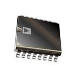
| 描述 | DGTL ISO 5KV RS422/RS485 16SOIC数字隔离器 5kV Sgnl Iso 500kbps Full/Half Duplex |
| 产品分类 | |
| 品牌 | Analog Devices Inc |
| 产品手册 | |
| 产品图片 |
|
| rohs | 符合RoHS无铅 / 符合限制有害物质指令(RoHS)规范要求 |
| 产品系列 | 接口 IC,数字隔离器,Analog Devices ADM2484EBRWZiCoupler® |
| 数据手册 | |
| 产品型号 | ADM2484EBRWZ |
| 上升/下降时间(典型值) | 1.1µs, 1.1µs (最小值) |
| 产品目录页面 | |
| 产品种类 | |
| 传播延迟tpLH/tpHL(最大值) | - |
| 供应商器件封装 | 16-SOIC |
| 共模瞬态抗扰度(最小值) | 25kV/µs |
| 关闭 | No Shutdown |
| 包装 | 管件 |
| 协议 | RS422,RS485 |
| 双工 | 全 |
| 商标 | Analog Devices |
| 安装类型 | 表面贴装 |
| 安装风格 | SMD/SMT |
| 封装 | Tube |
| 封装/外壳 | 16-SOIC(0.295",7.50mm 宽) |
| 封装/箱体 | SOIC-16 |
| 工作温度 | -40°C ~ 85°C |
| 工厂包装数量 | 47 |
| 技术 | 磁耦合 |
| 接收器滞后 | 15mV |
| 数据速率 | 500kbps |
| 最大工作温度 | + 85 C |
| 最大数据速率 | 500 kb/s |
| 最小工作温度 | - 40 C |
| 标准包装 | 47 |
| 电压-电源 | 3.3V,5V |
| 电压-隔离 | 5000Vrms |
| 电源电压-最大 | 5.5 V |
| 电源电压-最小 | 3 V |
| 电源电流 | 2 mA |
| 类型 | RS422, RS485 |
| 系列 | ADM2484E |
| 绝缘电压 | 5 kVrms |
| 脉宽失真(最大) | - |
| 输入-输入侧1/输入侧2 | 2/1 |
| 通道数 | 3 |
| 通道数量 | 3 Channel |
| 通道类型 | 单向 |
| 配用 | /product-detail/zh/EVAL-ADM2484EEBZ/EVAL-ADM2484EEBZ-ND/2342803 |
| 隔离式电源 | 是 |
| 驱动器/接收器数 | 1/1 |


- 商务部:美国ITC正式对集成电路等产品启动337调查
- 曝三星4nm工艺存在良率问题 高通将骁龙8 Gen1或转产台积电
- 太阳诱电将投资9.5亿元在常州建新厂生产MLCC 预计2023年完工
- 英特尔发布欧洲新工厂建设计划 深化IDM 2.0 战略
- 台积电先进制程称霸业界 有大客户加持明年业绩稳了
- 达到5530亿美元!SIA预计今年全球半导体销售额将创下新高
- 英特尔拟将自动驾驶子公司Mobileye上市 估值或超500亿美元
- 三星加码芯片和SET,合并消费电子和移动部门,撤换高东真等 CEO
- 三星电子宣布重大人事变动 还合并消费电子和移动部门
- 海关总署:前11个月进口集成电路产品价值2.52万亿元 增长14.8%


PDF Datasheet 数据手册内容提取
500 kbps, ESD Protected, Half-/Full-Duplex, iCoupler, Isolated RS-485 Transceiver Data Sheet ADM2484E FEATURES FUNCTIONAL BLOCK DIAGRAM Isolated, RS-485/RS-422 transceiver, configurable as half- or VDD1 VDD2 full-duplex ADM2484E ±15 kV ESD protection on RS-485 input/output pins DE 500 kbps data rate N O Complies with ANSI TIA/EIA RS-485-A-1998 and TI A ISO 8482: 1987(E) OL Y Suitable for 5 V or 3.3 V operation (VDD1) TxD NIC IS Z High common-mode transient immunity: >25 kV/μs VA L True fail-safe receiver inputs GA A 256 nodes on the bus RxD B Thermal shutdown protection RE SaUfeLt yre acnodg rneitgiuolna tory approvals GND1 GND2 06984-001 Figure 1. 5000 V rms isolation voltage for 1 minute per UL1577 VDE certificate of conformity DIN V VDE V 0884-10 (VDE V 0884-10): 2006-12 Reinforced insulation, V = 849 V IORM PEAK CSA Component Acceptance Notice 5A IEC 60950-1: 390 V rms (reinforced) Operating temperature range: −40°C to +85°C Wide body, 16-lead SOIC package APPLICATIONS Isolated RS-485/RS-422 interfaces Industrial field networks INTERBUS Multipoint data transmission systems GENERAL DESCRIPTION The ADM2484E is an isolated data transceiver with ±15 kV The differential transmitter outputs and receiver inputs feature ESD protection suitable for high speed, half- or full-duplex electrostatic discharge circuitry that provides protection up to communication on multipoint transmission lines. For half- ±15 kV using the human body model (HBM). The logic side of duplex operation, the transmitter outputs and receiver inputs the device can be powered with either a 5 V or a 3.3 V supply, share the same transmission line. Transmitter Output Pin Y whereas the bus side requires an isolated 3.3 V supply. links externally to Receiver Input Pin A, and Transmitter The device has current-limiting and thermal shutdown features Output Pin Z links externally to Receiver Input Pin B. to protect against output short circuits and situations where bus Designed for balanced transmission lines, the ADM2484E contention causes excessive power dissipation. complies with ANSI TIA/EIA RS-485-A-1998 and ISO 8482: 1987(E). The device employs Analog Devices, Inc., iCoupler® technology to combine a 3-channel isolator, a three-state differential line driver, and a differential input receiver into a single package. Rev. G Document Feedback Information furnished by Analog Devices is believed to be accurate and reliable. However, no responsibility is assumed by Analog Devices for its use, nor for any infringements of patents or other One Technology Way, P.O. Box 9106, Norwood, MA 02062-9106, U.S.A. rights of third parties that may result from its use. Specifications subject to change without notice. No license is granted by implication or otherwise under any patent or patent rights of Analog Devices. Tel: 781.329.4700 ©2008–2018 Analog Devices, Inc. All rights reserved. Trademarks and registered trademarks are the property of their respective owners. Technical Support www.analog.com
ADM2484E Data Sheet TABLE OF CONTENTS Features .............................................................................................. 1 Test Circuits ..................................................................................... 10 Applications ....................................................................................... 1 Switching Characteristics .............................................................. 11 Functional Block Diagram .............................................................. 1 Circuit Description......................................................................... 12 General Description ......................................................................... 1 Electrical Isolation ...................................................................... 12 Revision History ............................................................................... 2 Truth Tables................................................................................. 12 Specifications ..................................................................................... 3 Thermal Shutdown .................................................................... 13 Timing Specifications .................................................................. 4 True Fail-Safe Receiver Inputs .................................................. 13 Package Characteristics ............................................................... 4 Magnetic Field Immunity .......................................................... 13 Regulatory Information ............................................................... 4 Applications Information .............................................................. 14 Insulation and Safety-Related Specifications ............................ 5 Isolated Power Supply Circuit .................................................. 14 VDE 0884 Insulation Characteristics ........................................ 5 PC Board Layout ........................................................................ 14 Absolute Maximum Ratings ............................................................ 6 Typical Applications ................................................................... 15 ESD Caution .................................................................................. 6 Outline Dimensions ....................................................................... 16 Pin Configuration and Function Descriptions ............................. 7 Ordering Guide .......................................................................... 16 Typical Performance Characteristics ............................................. 8 REVISION HISTORY 11/2010—Rev. B to Rev. C Changes to Features Section ............................................................ 1 5/2018—Rev. F to Rev. G Changes to Table 4 ............................................................................. 4 Change to Features Section ............................................................. 1 Change to Maximum Working Insulation Voltage Parameter, Changes to Table 4 ............................................................................ 4 Table 6 .................................................................................................5 Changes to Figure 30 and Figure 31............................................. 15 11/2015—Rev. E to Rev. F Updated Outline Dimensions ....................................................... 16 Added Table 8; Renumbered Sequentially .................................... 6 Changes to Ordering Guide .......................................................... 16 3/2015—Rev. D to Rev. E 3/2010—Rev. A to Rev. B Changes to CTI Value and Isolation Group, Table 5 ................... 5 Changes to Minimum External Tracking (Creepage) Parameter, Table 5 .................................................................................................5 3/2014—Rev. C to Rev. D Changes to Features Section............................................................ 1 3/2009—Rev. 0 to Rev. A Changed V from 846 V to 849 V , Table 4 .................. 4 IORM PEAK PEAK Changes to Figure 28 ...................................................................... 14 Changes to VDE 0884 Insulation Characteristics Section .......... 5 Additional T Junction Temperature of 110°C, Table 7 ............... 6 J 5/2008—Revision 0: Initial Version Rev. G | Page 2 of 16
Data Sheet ADM2484E SPECIFICATIONS All voltages are relative to their respective grounds, 3.0 V ≤ V ≤ 5.5 V and 3.0 V ≤ V ≤ 3.6 V, all minimum/maximum specifications DD1 DD2 apply over the entire recommended operation range, all typical specifications are at T = 25°C, V = 5 V, andV = 3.3 V, unless A DD1 DD2 otherwise noted. Table 1. Parameter Symbol Min Typ Max Unit Test Conditions SUPPLY CURRENT Power Supply Current, Logic Side TxD/RxD Data Rate = 500 kbps I 2.0 mA Unloaded DD1 2.0 mA V = 3.6 V, half duplex configuration, DD2 R = 120 Ω, see Figure 20 TERMINATION Power Supply Current, Bus Side TxD/RxD Data Rate = 500 kbps I 3.0 mA Unloaded DD2 40 mA V = 3.6 V, half duplex configuration, DD2 R = 120 Ω, see Figure 20 TERMINATION DRIVER Differential Outputs Differential Output Voltage |V | 2.0 3.6 V Loaded, R = 100 Ω (RS-422), see OD L Figure 14 1.5 3.6 V R = 54 Ω (RS-485), see Figure 14 L 1.5 3.6 V −7 V ≤ V ≤ 12 V, see Figure 15 TEST ∆|V | for Complementary Output States ∆|V | 0.2 V R = 54 Ω or 100 Ω, see Figure 14 OD OD L Common-Mode Output Voltage V 3.0 V R = 54 Ω or 100 Ω, see Figure 14 OC L ∆|V | for Complementary Output States ∆|V | 0.2 V R = 54 Ω or 100 Ω, see Figure 14 OC OC L Output Leakage Current (Y, Z Pins) I 30 µA DE = 0 V, V = 0 V or 3.3 V, V = 12 V O DD2 IN −30 µA DE = 0 V, V = 0 V or 3.3 V, V = −7 V DD2 IN Short-Circuit Output Current I 250 mA OS Logic Inputs (DE, RE, TxD) Input Threshold Low V 0.25 × V V IL DD1 Input Threshold High V 0.7 × V V IH DD1 Input Current I −10 +0.01 +10 µA I RECEIVER Differential Inputs Differential Input Threshold Voltage V −200 −125 −30 mV −7 V < V < +12 V TH CM Input Voltage Hysteresis V 15 mV V = 0 V HYS OC Input Current (A, B) I 125 µA DE = 0 V, V = 0 V or 3.6 V, V = 12 V I DD IN −100 µA DE = 0 V, V = 0 V or 3.6 V, V = −7 V DD IN Line Input Resistance R 96 kΩ −7 V < V < +12 V IN CM Tristate Leakage Current I ±1 µA V = 5 V, 0 V < V < V OZR DD1 OUT DD1 Logic Outputs Output Voltage Low V 0.2 0.4 V I = 1.5 mA, V − V = −0.2 V OLRxD ORxD A B Output Voltage High V V − 0.3 V − 0.2 V I = −1.5 mA, V − V = +0.2 V OHRxD DD1 DD1 ORxD A B Short-Circuit Current 100 mA COMMON-MODE TRANSIENT IMMUNITY1 25 kV/µs V = 1 kV, transient magnitude = 800 V CM 1 CM is the maximum common-mode voltage slew rate that can be sustained while maintaining specification-compliant operation. VCM is the common-mode potential difference between the logic and bus sides. The transient magnitude is the range over which the common mode is slewed. The common-mode voltage slew rates apply to both rising and falling common-mode voltage edges. Rev. G | Page 3 of 16
ADM2484E Data Sheet TIMING SPECIFICATIONS T = −40°C to +85°C. A Table 2. Parameter Symbol Min Typ Max Unit Test Conditions DRIVER Propagation Delay t , t 250 700 ns R = 54 Ω, C = C = 100 pF, see Figure 16 and Figure 21 DPLH DPHL L L1 L2 Differential Driver Output Skew t 100 ns R = 54 Ω, C = C = 100 pF, see Figure 16 and Figure 21 DSKEW L L1 L2 (t − t ) DPLH DPHL Rise Time/Fall Time t , t 200 450 1100 ns R = 54 Ω, C = C = 100 pF, see Figure 16 and Figure 21 DR DF L L1 L2 Enable Time t , t 1.5 µs R = 110 Ω, C = 50 pF, see Figure 18 and Figure 22 ZL ZH L L Disable Time t , t 200 ns R = 110 Ω, C = 50 pF, see Figure 18 and Figure 22 LZ HZ L L RECEIVER Propagation Delay t , t 200 ns C = 15 pF, see Figure 17 and Figure 23 PLH PHL L Pulse Width Distortion, t 30 ns C = 15 pF, see Figure 17 and Figure 23 PWD L PWD = |t − t | PLH PHL Enable Time t , t 13 ns R = 1 kΩ, C = 15 pF, see Figure 19 and Figure 24 ZL ZH L L Disable Time t , t 13 ns R = 1 kΩ, C = 15 pF, see Figure 19 and Figure 24 LZ HZ L L PACKAGE CHARACTERISTICS Table 3. Parameter Symbol Min Typ Max Unit Test Conditions RESISTANCE Resistance (Input-to-Output)1 R 1012 Ω I-O CAPACITANCE Capacitance (Input-to-Output)1 C 3 pF f = 1 MHz I-O Input Capacitance2 C 4 pF I THERMAL RESISTANCE Input IC Junction-to-Case θ 33 °C/W Thermocouple located at center of package underside JCI Output IC Junction-to-Case θ 28 °C/W JCO 1 Device considered a 2-terminal device: Pin 1 to Pin 8 are shorted together and Pin 9 to Pin16 are shorted together. 2 Input capacitance is from any input data pin to ground. REGULATORY INFORMATION Table 4. UL1 CSA VDE2 UL 1577 Component Approved under CSA Component Acceptance Notice 5A, Certified according to DIN V VDE V 0884-10 Recognition Program CSA 60950-1-07+A1+A2 and IEC 60950-1 second edition +A1+A2: (VDE V 0884-10): 2006-122 Basic insulation at 780 V rms (1103 V peak) Reinforced insulation at 390 V rms (552 V peak) CSA 61010-1-12+A1 and IEC 61010-1 third edition: Basic 600 V rms, Overvoltage Category III Reinforced 300 V rms, Overvoltage Category III 5000 V rms Isolation Voltage Reinforced insulation, 849 V PEAK 1 In accordance with UL1577, each ADM2484E is proof tested by applying an insulation test voltage ≥ 6000 V rms for 1 second (current leakage detection limit = 10 µA). 2 In accordance with DIN V VDE V 0884-10, each ADM2484E is proof tested by applying an insulation test voltage ≥ 1590 VPEAK for 1 second (partial discharge detection limit = 5 pC). Rev. G | Page 4 of 16
Data Sheet ADM2484E INSULATION AND SAFETY-RELATED SPECIFICATIONS Table 5. Parameter Symbol Value Unit Conditions Rated Dielectric Insulation Voltage 5000 V rms 1-minute duration Minimum External Air Gap (Clearance) L(I01) 7.7 mm min Measured from input terminals to output terminals, shortest distance through air Minimum External Tracking (Creepage) L(I02) 7.6 mm min Measured from input terminals to output terminals, shortest distance along body Minimum Internal Gap (Internal Clearance) 0.017 mm min Insulation distance through insulation Tracking Resistance (Comparative Tracking Index) CTI >400 V DIN IEC 112/VDE 0303 Part 1 Isolation Group II Material Group (DIN VDE 0110, 1/89, Table 1) VDE 0884 INSULATION CHARACTERISTICS This isolator is suitable for reinforced electrical isolation only within the safety limit data. Maintenance of the safety data must be ensured by means of protective circuits. An asterisk (*) on a package denotes VDE 0884 approval for 849 V working voltage. PEAK Table 6. Description Conditions Symbol Characteristic Unit CLASSIFICATIONS Installation Classification per DIN VDE 0110 for Rated Mains Voltage ≤300 V rms I to IV ≤450 V rms I to II ≤600 V rms I to II Climatic Classification 40/105/21 Pollution Degree DIN VDE 0110, see Table 1 2 VOLTAGE Maximum Working Insulation Voltage V 849 V IORM PEAK Input-to-Output Test Voltage V PR Method b1 V × 1.875 = V , 100% production tested, 1590 V IORM PR PEAK t = 1 sec, partial discharge < 5 pC m Method a After Environmental Tests, Subgroup 1 V × 1.6 = V , t = 60 sec, partial 1357 V IORM PR m PEAK discharge < 5 pC After Input and/or Safety Test, V × 1.2 = V , t = 60 sec, partial 1018 V IORM PR m PEAK Subgroup 2/Subgroup 3 discharge < 5 pC Highest Allowable Overvoltage (Transient overvoltage, t = 10 sec) V 6000 V TR TR PEAK SAFETY-LIMITING VALUES Maximum value allowed in the event of a failure, see Figure 9 Case Temperature T 150 °C S Input Current I, 265 mA S INPUT Output Current I, 335 mA S OUTPUT Insulation Resistance at T V = 500 V R >109 Ω S IO S Rev. G | Page 5 of 16
ADM2484E Data Sheet ABSOLUTE MAXIMUM RATINGS T = 25°C, unless otherwise noted. Each voltage is relative to its Table 8. Maximum Continuous Working Voltage1 A respective ground. Parameter Max Unit Reference Standard AC Voltage Table 7. Bipolar Waveform Parameter Rating Basic Insulation 565 V 50-year minimum PEAK VDD1 −0.5 V to +7 V lifetime VDD2 −0.5 V to +6 V Reinforced Insulation 565 VPEAK 50-year minimum Logic Input Voltages −0.5 V to VDD1 + 0.5 V lifetime Bus Terminal Voltages −9 V to +14 V Unipolar Waveform Logic Output Voltages −0.5 V to VDD1 + 0.5 V Basic Insulation 1131 VPEAK 50-year minimum Average Output Current per Pin ±35 mA lifetime ESD (Human Body Model) on A, B, Y, ±15 kV Reinforced Insulation 864 VPEAK Lifetime limited by and Z Pins package creepage maximum approved Storage Temperature Range −55°C to +150°C working voltage per Ambient Operating Temperature Range −40°C to +85°C IEC 60950-1 θ Thermal Impedance 73°C/W JA DC Voltage T Junction Temperature 110°C J Basic Insulation 1066 V Lifetime limited by PEAK package creepage maximum approved Stresses at or above those listed under Absolute Maximum working voltage per Ratings may cause permanent damage to the product. This is a IEC 60950-1 stress rating only; functional operation of the product at these Reinforced Insulation 529 VPEAK Lifetime limited by or any other conditions above those indicated in the operational package creepage maximum approved section of this specification is not implied. Operation beyond working voltage per the maximum operating conditions for extended periods may IEC 60950-1 affect product reliability. 1 Refers to continuous voltage magnitude imposed across the isolation Absolute maximum ratings apply individually only, not in barrier. combination. ESD CAUTION Rev. G | Page 6 of 16
Data Sheet ADM2484E PIN CONFIGURATION AND FUNCTION DESCRIPTIONS VDD1 1 16 VDD2 GND1 2 15 GND2 RxD 3 ADM2484E 14 A RE 4 TOP VIEW 13 B DE 5 (Not to Scale) 12 Z TxD 6 11 Y NC 7 10 NC GND1 8NC = NO CONNECT9 GND2 06984-002 Figure 2. Pin Configuration Table 9. Pin Function Descriptions Pin No. Mnemonic Description 1 V Power Supply (Logic Side). Decoupling capacitor to GND required; capacitor value should be between 0.01 µF and 0.1 µF. DD1 1 2 GND Ground (Logic Side). 1 3 RxD Receiver Output. 4 RE Receiver Enable Input. Active low logic input. When this pin is low, the receiver is enabled; when this pin is high, the receiver is disabled. 5 DE Driver Enable Input. Active high logic input. When this pin is high, the driver (transmitter) is enabled; when this pin is low, the driver is disabled. 6 TxD Transmit Data. 7 NC No Connect. This pin must be left floating. 8 GND Ground (Logic Side). 1 9 GND Ground (Bus Side). 2 10 NC No Connect. This pin must be left floating. 11 Y Driver Noninverting Output. 12 Z Driver Inverting Output. 13 B Receiver Inverting Input. 14 A Receiver Noninverting Input. 15 GND Ground (Bus Side). 2 16 V Power Supply (Bus Side). Decoupling capacitor to GND required; capacitor value should be between 0.01 µF and 0.1 µF. DD2 2 Rev. G | Page 7 of 16
ADM2484E Data Sheet TYPICAL PERFORMANCE CHARACTERISTICS 1.4 100 DATA RATE = 500kbps 1.2 90 tPHL A) 80 tPLH T (m 1.0 N54OΩ L LOOAADD 70 N 100Ω LOAD Y CURRE 0.8 LAY (ns) 6500 L 0.6 E P D 40 P U SD1 0.4 30 D I 20 0.2 0 06984-033 100 06984-035 –40 –20 0 20 40 60 80 –40 –20 0 20 40 60 80 TEMPERATURE (°C) TEMPERATURE (°C) Figure 3. IDD1 Supply Current vs. Temperature (See Figure 20) Figure 6. Receiver Propagation Delay vs. Temperature 45 DATA RATE = 500kbps T 40 54Ω LOAD A) 35 m NT ( 30 100Ω LOAD TxD E R 1 R 25 U C LY 20 Z, B P P SU 15 2 Y, A D2 ID 10 NO LOAD 50–40 –20 0 20 40 60 80 06984-034 4 RxD 06984-031 CH1 2.00V CH2 2.00V M 200ns A CH2 1.72V TEMPERATURE (°C) CH3 2.00V CH4 2.00V T 47.80% Figure 4. IDD2 Supply Current vs. Temperature (See Figure 20) Figure 7. Driver/Receiver Propagation Delay, Low to High (RL = 54 Ω, CL1 = CL2 = 100 pF) 600 tDPLH T 500 tDPHL 400 TxD ns) 1 AY ( 300 EL Z, B D 200 2 Y, A 100 0–40 –20 0 20 40 60 80 06984-032 4 RxD 06984-030 CH1 2.00V CH2 2.00V M 200ns A CH2 1.72V TEMPERATURE (°C) CH3 2.00V CH4 2.00V T 48.60% Figure 5. Driver Propagation Delay vs. Temperature Figure 8. Driver/Receiver Propagation Delay, High to Low (RL = 54 Ω, CL1 = CL2 = 100 pF) Rev. G | Page 8 of 16
Data Sheet ADM2484E 350 4.77 4.76 300 A) 4.75 m T ( 250 4.74 CURREN 200 SIDE 2 AGE (V) 44..7723 G LT N O 4.71 TI 150 V MI SIDE 1 4.70 LI TY- 100 4.69 E F A 4.68 S 50 0 06984-016 44..6667 06984-019 0 50 100 150 200 –40 –20 0 20 40 60 80 100 CASE TEMPERATURE (°C) TEMPERATURE (°C) Figure 9. Thermal Derating Curve, Dependence of Safety-Limiting Values Figure 12. Receiver Output High Voltage vs. Temperature, IRxD = −4 mA with Case Temperature per VDE 0884 0 0.35 –2 0.30 –4 0.25 NT (mA) –6 TAGE (V) 0.20 E L R O R –8 V 0.15 U C –10 0.10 ––1142 06984-017 0.050 06984-022 4.0 4.2 4.4 4.6 4.8 5.0 –40 –20 0 20 40 60 80 100 VOLTAGE (V) TEMPERATURE (°C) Figure 10. Output Current vs. Receiver Output High Voltage Figure 13. Receiver Output Low Voltage vs. Temperature, IRxD = +4 mA 16 14 12 A) 10 m T ( EN 8 R R CU 6 4 02 06984-018 0 0.2 0.4 0.6 0.8 1.0 1.2 VOLTAGE (V) Figure 11. Output Current vs. Receiver Output Low Voltage Rev. G | Page 9 of 16
ADM2484E Data Sheet TEST CIRCUITS RL 2 A VOD R2L VOC 06984-003 B CL VOUT 06984-007 Figure 14. Driver Voltage Measurement Figure 17. Receiver Propagation Delay 375Ω VOUT VCC Y VOD 60Ω VTEST RL 0V OR 3V S1 S2 375Ω 06984-004 DE Z CL 06984-008 Figure 15. Driver Voltage Measurement Figure 18. Driver Enable/Disable +1.5V VCC S1 Y CL1 –1.5V RL Z RL CL2 06984-006 RE IN RE CVOLUT S2 06984-009 Figure 16. Driver Propagation Delay Figure 19. Receiver Enable/Disable VDD2 VDD1 VDD2 DE N O TI A L Y O TxD C IS Z 120Ω NI A V L A A G RxD B RE GND1 GND2 06984-005 Figure 20. Supply Current Measurement Test Circuit Rev. G | Page 10 of 16
Data Sheet ADM2484E SWITCHING CHARACTERISTICS VDD1 VDD1/2 VDD1/2 0V tDPLH tDPHL Z A, B 1/2VO 0V 0V VO Y tPLH tPHL +VO 90% POINT VDIFF = V(Y) – V(Z) 90% POINT VOH VDIFF RxD 1.5V 1.5V –VO 10% POINT tDR tDF 10% POINT 06984-010 VOL 06984-012 Figure 21. Driver Propagation Delay, Rise/Fall Timing Figure 23. Receiver Propagation Delay VDD1 VDD1 RE 0.5VDD1 0.5VDD1 DE 0.5VDD1 0.5VDD1 0V 0V tZL tLZ tZL tLZ RxD 1.5V Y,Z 2.3V VOL + 0.5V OUTPUT LOW VOL + 0.5V VOL VOL tZH tHZ tZH tHZ OUTPUT HIGH Y,Z VOH – 0.5V VOH RxD VOH – 0.5V VOH 2.3V 0V 06984-011 0V 1.5V 0V 06984-013 Figure 22. Driver Enable/Disable Delay Figure 24. Receiver Enable/Disable Delay Rev. G | Page 11 of 16
ADM2484E Data Sheet CIRCUIT DESCRIPTION ELECTRICAL ISOLATION TRUTH TABLES In the ADM2484E, electrical isolation is implemented on the The truth tables in this section use the abbreviations shown logic side of the interface. Therefore, the part has two main in Table 10. sections: a digital isolation section and a transceiver section Table 10. Truth Table Abbreviations (see Figure 25). The driver input signal, which is applied to the Letter Description TxD pin and referenced to the logic ground (GND), is coupled 1 H High level across an isolation barrier to appear at the transceiver section L Low level referenced to the isolated ground (GND). Similarly, the receiver 2 I Indeterminate input, which is referenced to the isolated ground in the transceiver X Irrelevant section, is coupled across the isolation barrier to appear at the Z High impedance (off) RxD pin referenced to the logic ground. NC Disconnected iCoupler Technology The digital signals transmit across the isolation barrier using Table 11. Transmitting iCoupler technology. This technique uses chip scale transformer Supply Status Inputs Outputs windings to couple the digital signals magnetically from one VDD1 VDD2 DE TxD Y Z side of the barrier to the other. Digital inputs are encoded into On On H H H L waveforms that are capable of exciting the primary transformer On On H L L H winding. At the secondary winding, the induced waveforms are On On L X Z Z decoded into the binary value that was originally transmitted. On Off X X Z Z Off On L X Z Z Positive and negative logic transitions at the input cause narrow Off Off X X Z Z (approximately 1 ns) pulses to be sent to the decoder via the transformer. The decoder is bistable and is, therefore, set or reset Table 12. Receiving by the pulses, indicating input logic transitions. In the absence of Supply Status Inputs Output logic transitions at the input for more than approximately 1 μs, V V A − B (V) RE RxD a periodic set of refresh pulses, indicative of the correct input DD1 DD2 On On > −0.03 L or NC H state, are sent to ensure dc correctness at the output. If the On On < −0.2 L or NC L decoder receives no internal pulses for more than about 5 μs, On On −0.2 < A − B < −0.03 L or NC I then the input side is assumed to be unpowered or nonfunctional, On On Inputs open L or NC H in which case the output is forced to a default state (see Table 11). On On X H Z VDD1 VDD2 On Off X L or NC H ISOLATION BARRIER Off Off X L or NC L DE ENCODE DECODE Y TxD ENCODE DECODE D Z A RxD DECODE ENCODE R B RE DIGITAL ISOLATION TRANSCEIVER 06984-023 GND1 GND2 Figure 25. Digital Isolation and Transceiver Sections Rev. G | Page 12 of 16
Data Sheet ADM2484E THERMAL SHUTDOWN 100 The ADM2484E contains thermal shutdown circuitry that C protects the part from excessive power dissipation during fault TI 10 E csoounrdcitei ocnasn. Srehsourltti ning hthigeh d drirviveer ro cuutprruetns ttso. Ta hloew th iemrmpeadl asnences ing E MAGNGAUSS) 1 Lk circuitry detects the increase in die temperature under this ABY ( cdoensidgintieodn t oan ddi sdaibslaeb tlhese tdhrei vderri voeurt pouuttsp uwths.e Tn hai sd cieir tceumitpryer iast ure ALLOWDENSIT 0.1 of 150°C is reached. As the device cools, the drivers re-enable at MUM FLUX a temperature of 140°C. AXI 0.01 M TRUE FAIL-SAFE RECEIVER INPUTS 0.001 06984-024 The receiver inputs have a true fail-safe feature ensuring that 1k 10k 100k 1M 10M 100M the receiver output is high when the inputs are open or shorted. MAGNETIC FIELD FREQUENCY (Hz) Figure 26. Maximum Allowable External Magnetic Flux Density During line-idle conditions, when no driver on the bus is enabled, the voltage across a terminating resistor at the receiver input decays For example, at a magnetic field frequency of 1 MHz, the to 0 V. With traditional transceivers, receiver input thresholds maximum allowable magnetic field of 0.2 kgauss induces a specified between −200 mV and +200 mV mean that external voltage of 0.25 V at the receiving coil. This is about 50% of the bias resistors are required on the A and B pins to ensure that the sensing threshold and does not cause a faulty output transition. receiver outputs are in a known state. The true fail-safe receiver Similarly, if such an event occurs during a transmitted pulse and input feature eliminates the need for bias resistors by specifying is the worst-case polarity, it reduces the received pulse from the receiver input threshold between −30 mV and −200 mV. >1.0 V to 0.75 V, still well above the 0.5 V sensing threshold of The guaranteed negative threshold means that when the voltage the decoder. between A and B decays to 0 V; the receiver output is guaran- Figure 27 shows the magnetic flux density values in terms of teed to be high. more familiar quantities, such as maximum allowable current MAGNETIC FIELD IMMUNITY flow at given distances away from the ADM2484E transformers. The limitation on the magnetic field immunity of the iCoupler 1000 is set by the condition in which an induced voltage in the receiving A) DISTANCE = 1m coil of the transformer is large enough to either falsely set or reset T (k 100 the decoder. The following analysis defines the conditions under EN R which this may occur. The 3 V operating condition of the UR DISTANCE = 5mm ADM2484E is examined because it represents the most E C 10 L B susceptible mode of operation. A W DISTANCE = 100mm The pulses at the transformer output have an amplitude greater LLO 1 A then 1 V. The decoder has a sensing threshold of about 0.5 V, M U M thus establishing a 0.5 V margin in which induced voltages can XI 0.1 A bTeh eto vleorltaategde .i n duced across the receiving coil is given by M 0.01 06984-025 1k 10k 100k 1M 10M 100M −dβ MAGNETIC FIELD FREQUENCY (Hz) V = dt ∑πrn2; n=1,2,...,N Figure 27. Maximum Allowable Current for Various Current-to-ADM2484E Spacings where: With combinations of strong magnetic field and high frequency, β is the magnetic flux density (gauss). any loops formed by PCB traces can induce error voltages large N is the number of turns in the receiving coil. enough to trigger the thresholds of succeeding circuitry. Take care r is the radius of the nth turn in the receiving coil (cm). n in the layout of such traces to avoid this possibility. Given the geometry of the receiving coil and an imposed requirement that the induced voltage is, at most, 50% of the 0.5 V margin at the decoder, a maximum allowable magnetic field can be determined using Figure 26. Rev. G | Page 13 of 16
ADM2484E Data Sheet APPLICATIONS INFORMATION ISOLATED POWER SUPPLY CIRCUIT PC BOARD LAYOUT The ADM2484E requires isolated power capable of 3.3 V at up The ADM2484E isolated RS-485 transceiver requires no external to approximately 75 mA (this current is dependent on the data interface circuitry for the logic interfaces. Power supply bypassing rate and termination resistors used) to be supplied between the is required at the input and output supply pins (see Figure 29). V and the GND pins. A transformer driver circuit with a Bypass capacitors are conveniently connected between Pin 1 DD2 2 center tapped transformer and LDO can be used to generate the and Pin 2 for V and between Pin 15 and Pin 16 for V . DD1 DD2 isolated 5 V supply, as shown in Figure 28. The center tapped Best practice suggests the following: transformer provides electrical isolation of the 5 V power • A capacitor value between 0.01 µF and 0.1 µF. supply. The primary winding of the transformer is excited with • A total lead length between both ends of the capacitor and a pair of square waveforms that are 180° out of phase with each the input power supply pin that does not exceed 20 mm. other. A pair of Schottky diodes and a smoothing capacitor are • Unless the ground pair on each package side is connected used to create a rectified signal from the secondary winding. close to the package, consider bypassing between Pin 1 and The ADP3330 linear voltage regulator provides a regulated Pin 8 and between Pin 9 and Pin 16. power supply to the bus-side circuitry (V ) of the ADM2484E. DD2 VCC ISBOALRARTIEIORN GVNDDD11 VGDNDD22 SD103C RxD A 3.3V RE ADM2484E B TRADNRSIFVOERRMER VCC +22µF ISENRDRADP3O3U3T0 +10µF TNDxCDE ZNYC 78253 SD103C NR GND GND1 NC = NO CONNECT GND2 06984-027 VCC Figure 29. Recommended PCB Layout VDD1 VDD2 In applications involving high common-mode transients, ensure that board coupling across the isolation barrier is minimized. ADM2484E Furthermore, design the board layout so that any coupling that GND1 GND2 06984-026 dFaoielus roec tcou re nesquurael ltyh aisf fceocutsl da lcl apuisnes v oonlt aag gei dveifnfe creonmtipaolsn beenttw siedeen. pins Figure 28. Isolated Power Supply Circuit exceeding the absolute maximum ratings of the device, thereby leading to latch-up or permanent damage. Rev. G | Page 14 of 16
Data Sheet ADM2484E TYPICAL APPLICATIONS at the receiving end in its characteristic impedance, and stub lengths off the main line must be kept as short as possible. For Figure 30 and Figure 31 show typical applications of the half-duplex operation, this means that both ends of the line must be ADM2484E in half-duplex and full-duplex RS-485 network terminated, because either end can be the receiving end. configurations. Up to 256 transceivers can be connected to the RS-485 bus. To minimize reflections, the line must be terminated MAXIMUM NUMBER OF TRANSCEIVERS ON BUS = 256 ADM2484E ADM2484E A A RxD R B B R RxD RE RE RT RT DE DE Z Z TxD D Y Y D TxD A B Z Y A B Z Y R R D D ADM2484E ADM2484E RxD RE DE TxD RxD RE DE TxD N1.O RTTE ISS EQUAL TO THE CHARACTERISTIC IMPEDANCE OF THE CABLE. 06984-028 2. ISOLATION NOT SHOWN. Figure 30. ADM2484E Typical Half-Duplex RS-485 Network MAXIMUM NUMBER OF NODES = 256 MASTER SLAVE A Y RxD R RT D TxD B Z RE DE DE Z B RE TxD D Y RT A R RxD ADM2484E ADM2484E A B Z Y A B Z Y SLAVE SLAVE R R D D ADM2484E ADM2484E RxD RE DE TxD RxD RE DE TxD N1.O RTTE ISS EQUAL TO THE CHARACTERISTIC IMPEDANCE OF THE CABLE. 06984-029 Figure 31. ADM2484E Typical Full Duplex RS-485 Network Rev. G | Page 15 of 16
ADM2484E Data Sheet OUTLINE DIMENSIONS 10.50(0.4134) 10.10(0.3976) 16 9 7.60(0.2992) 7.40(0.2913) 1 8 10.65(0.4193) 10.00(0.3937) 1.27(0.0500) 0.75(0.0295) BSC 2.65(0.1043) 0.25(0.0098) 45° 0.30(0.0118) 2.35(0.0925) 8° 0.10(0.0039) 0° COPLANARITY 0.10 0.51(0.0201) SPELAATNIENG 0.33(0.0130) 1.27(0.0500) 0.31(0.0122) 0.20(0.0079) 0.40(0.0157) (RCINEOFNPEATRRREOENNLCLTEIHNCEOGOSNDMELISPYM)LAEAIANNRNDSETIAORTRNOOESUJNANEORDDETEEDAICN-POSMPFTRIFALONLMPIDMIRLAELIRATIMTDEEESRTFSMEO;SRIRN-0ECU1QH3SU-EADIVAIINMAELDENENSSTIIOGSNNFS.OR 2007-B03-27- Figure 32. 16-Lead Standard Small Outline Package [SOIC_W] Wide Body (RW-16) Dimensions shown in millimeters and (inches) ORDERING GUIDE Model1 Temperature Range Package Description Package Option ADM2484EBRWZ −40°C to +85°C 16-Lead Standard Small Outline Package [SOIC_W] RW-16 ADM2484EBRWZ-REEL7 −40°C to +85°C 16-Lead Standard Small Outline Package [SOIC_W] RW-16 EVAL-ADM2484EEBZ Evaluation Board 1 Z = RoHS Compliant Part. ©2008–2018 Analog Devices, Inc. All rights reserved. Trademarks and registered trademarks are the property of their respective owners. D06984-0-5/18(G) Rev. G | Page 16 of 16
Mouser Electronics Authorized Distributor Click to View Pricing, Inventory, Delivery & Lifecycle Information: A nalog Devices Inc.: ADM2484EBRWZ EVAL-ADM2484EEBZ ADM2484EBRWZ-REEL7