ICGOO在线商城 > 集成电路(IC) > PMIC - 热插拔控制器 > ADM1177-1ARMZ-R7
 Datasheet下载
- 型号: ADM1177-1ARMZ-R7
- 制造商: Analog
- 库位|库存: xxxx|xxxx
- 要求:
| 数量阶梯 | 香港交货 | 国内含税 |
| +xxxx | $xxxx | ¥xxxx |
查看当月历史价格
查看今年历史价格
ADM1177-1ARMZ-R7产品简介:
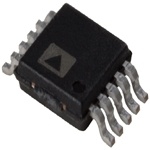
ICGOO电子元器件商城为您提供ADM1177-1ARMZ-R7由Analog设计生产,在icgoo商城现货销售,并且可以通过原厂、代理商等渠道进行代购。 ADM1177-1ARMZ-R7价格参考¥33.18-¥50.75。AnalogADM1177-1ARMZ-R7封装/规格:PMIC - 热插拔控制器, Hot Swap Controller, Monitor 1 Channel General Purpose 10-MSOP。您可以下载ADM1177-1ARMZ-R7参考资料、Datasheet数据手册功能说明书,资料中有ADM1177-1ARMZ-R7 详细功能的应用电路图电压和使用方法及教程。
Analog Devices Inc.(ADI公司)的ADM1177-1ARMZ-R7是一款PMIC(电源管理集成电路),特别设计用于热插拔控制器应用。它广泛应用于数据中心、服务器、通信设备、存储系统以及其他需要高可靠性和热插拔功能的电子设备中。

 主要应用场景:

1. 数据中心与服务器:
   - 在数据中心和服务器环境中,热插拔功能至关重要。ADM1177-1ARMZ-R7能够确保在不断电的情况下安全插入或移除板卡,避免对整个系统的冲击和损坏。它通过精确控制电流限制和电压调节,防止过流和短路,保护敏感的电路组件。

2. 通信设备:
   - 通信设备如路由器、交换机等需要频繁更换模块或板卡,而这些操作通常在带电状态下进行。ADM1177-1ARMZ-R7可以确保在这些操作过程中,电源的平稳过渡,减少对其他模块的影响,提高系统的稳定性和可靠性。

3. 存储系统:
   - 存储系统中的硬盘驱动器(HDD)或固态硬盘(SSD)往往支持热插拔功能。该芯片可以帮助实现这一功能,确保在插入或拔出存储设备时,电源的平稳切换,避免数据丢失或硬件损坏。

4. 工业自动化设备:
   - 在工业自动化领域,许多设备需要具备热插拔功能以方便维护和升级。ADM1177-1ARMZ-R7可以用于控制这些设备的电源输入,确保在不停机的情况下进行模块更换,从而提高生产效率。

5. 医疗设备:
   - 医疗设备中的一些模块也需要支持热插拔功能,以便在不影响设备运行的情况下进行维护或升级。该芯片可以在这些场景中提供可靠的电源管理和保护功能,确保设备的安全性和稳定性。

 总结:
ADM1177-1ARMZ-R7凭借其高效的电流限制、电压调节和故障保护功能,在各种需要热插拔功能的高可靠性应用中表现出色。它不仅提高了系统的安全性,还简化了维护和升级过程,适用于数据中心、通信设备、存储系统、工业自动化和医疗设备等多种场合。
| 参数 | 数值 |
| 产品目录 | 集成电路 (IC) |
| 描述 | IC CTRLR HOTSWAP 16.5V 10-MSOP |
| 产品分类 | |
| 品牌 | Analog Devices Inc |
| 数据手册 | |
| 产品图片 |
|
| 产品型号 | ADM1177-1ARMZ-R7 |
| rohs | 无铅 / 符合限制有害物质指令(RoHS)规范要求 |
| 产品系列 | - |
| 产品培训模块 | http://www.digikey.cn/PTM/IndividualPTM.page?site=cn&lang=zhs&ptm=3921 |
| 供应商器件封装 | 10-MSOP |
| 其它名称 | ADM1177-1ARMZ-R7CT |
| 内部开关 | 无 |
| 功能引脚 | ON, SS, TIMER |
| 包装 | 剪切带 (CT) |
| 可编程特性 | 限流,故障超时,开启电压 |
| 安装类型 | 表面贴装 |
| 封装/外壳 | 10-TFSOP,10-MSOP(0.118",3.00mm 宽) |
| 工作温度 | -40°C ~ 85°C |
| 应用 | 通用 |
| 标准包装 | 1 |
| 特性 | 自动重试,I2C,UVLO |
| 电压-电源 | 3.15 V ~ 16.5 V |
| 电流-电源 | 1.7mA |
| 电流-输出(最大值) | - |
| 类型 | 热交换控制器, 监控器 |
| 视频文件 | http://www.digikey.cn/classic/video.aspx?PlayerID=1364138032001&width=640&height=505&videoID=1706665791001 |
| 通道数 | 1 |
| 配用 | /product-detail/zh/EVAL-ADM1177EBZ/EVAL-ADM1177EBZ-ND/1305600 |


- 商务部:美国ITC正式对集成电路等产品启动337调查
- 曝三星4nm工艺存在良率问题 高通将骁龙8 Gen1或转产台积电
- 太阳诱电将投资9.5亿元在常州建新厂生产MLCC 预计2023年完工
- 英特尔发布欧洲新工厂建设计划 深化IDM 2.0 战略
- 台积电先进制程称霸业界 有大客户加持明年业绩稳了
- 达到5530亿美元!SIA预计今年全球半导体销售额将创下新高
- 英特尔拟将自动驾驶子公司Mobileye上市 估值或超500亿美元
- 三星加码芯片和SET,合并消费电子和移动部门,撤换高东真等 CEO
- 三星电子宣布重大人事变动 还合并消费电子和移动部门
- 海关总署:前11个月进口集成电路产品价值2.52万亿元 增长14.8%


PDF Datasheet 数据手册内容提取
Hot Swap Controller and Digital Power Monitor with Soft Start Pin Data Sheet ADM1177 FEATURES FUNCTIONAL BLOCK DIAGRAM Allows safe board insertion and removal from ADM1177 a live backplane MUX Controls supply voltages from 3.15 V to 16.5 V V Precision current sense amplifier VCC 0 12-BIT SDA Precision voltage input I ADC I2C SCL 12-bit ADC for current and voltage readback A 1 SENSE ADR Charge pumped gate drive for external N-channel FET CURRENT Adjustable analog current limit with circuit breaker SENSE AMPLIFIER ±3% accurate hot swap current limit level Fast response limits peak fault current ON FET DRIVE Automatic retry or latch-off on current fault CONTROLLER GATE 1.3V Programmable hot swap timing via TIMER pin UV COMPARATOR Soifnt isttiaalr tc uprinre fnotr r raemfepre rnatcee adjustment and programming of GND SS TIMER 06047-001 Active high ON pin Figure 1. I2C fast mode-compliant interface (400 kHz maximum) 10-lead MSOP 3.15V TO 16.5V RSENSE N-CHANNEL FET APPLICATIONS Power monitoring/power budgeting VCC SENSE CONTROLLER Central office equipment GATE Telecommunications and data communications equipment ADM1177 P = VI PCs/servers ON SDA SDA GENERAL DESCRIPTION SCL SCL SS The ADM1177 is an integrated hot swap controller that offers TIMER danigailtoagl -ctuor-rdeingtit aanl dco vnovletargteer m (AoDniCto)r, icnogm vmia uanni coant-ecdh tiph,r o1u2-gbhi ta n GND ADR 06047-002 I2C® interface. Figure 2. Applications Diagram An internal current sense amplifier measures voltage across the sense resistor in the power path via the VCC pin and the A soft start pin (SS) is also included. This gives the user control SENSE pin. over the reference on the current sense amplifier. An internal The ADM1177 limits the current through this resistor by current source charges a capacitor on this pin at startup, allowing controlling the gate voltage (via the GATE pin) of an external the user to set the profile of the initial current ramp. A voltage N-channel FET in the power path. The voltage across the sense can also be driven on this pin to alter the reference. resistor (and, therefore, the inrush current) is kept below a A 12-bit ADC can measure the current seen in the sense resistor, preset maximum. as well as the supply voltage on the VCC pin. An industry-standard The ADM1177 protects the external FET by limiting the time I2C interface allows a controller to read current and voltage data that the maximum current runs through it. This current limit from the ADC. Measurements can be initiated by an I2C command. period is set by the value of the capacitor attached to the TIMER Alternatively, the ADC can run continuously, and the user can pin. Additionally, the device provides protection from overcurrent read the latest conversion data whenever it is required. Up to events that may occur once the hot swap event is complete. In four unique I2C addresses can be created, depending on how the the case of a short-circuit event, the current in the sense resistor ADR pin is connected. exceeds an overcurrent trip threshold, and the FET is switched off The ADM1177 is packaged in a 10-lead MSOP. immediately by pulling down the GATE pin. Rev. C Document Feedback Information furnished by Analog Devices is believed to be accurate and reliable. However, no responsibility is assumed by Analog Devices for its use, nor for any infringements of patents or other One Technology Way, P.O. Box 9106, Norwood, MA 02062-9106, U.S.A. rights of third parties that may result from its use. Specifications subject to change without notice. No license is granted by implication or otherwise under any patent or patent rights of Analog Devices. Tel: 781.329.4700 ©2006–2012 Analog Devices, Inc. All rights reserved. Trademarks and registered trademarks are the property of their respective owners. Technical Support www.analog.com
ADM1177 Data Sheet TABLE OF CONTENTS Features .............................................................................................. 1 Initial Timing Cycle ................................................................... 13 Applications ....................................................................................... 1 Hot Swap Retry Cycle on the ADM1177-1 ............................. 14 General Description ......................................................................... 1 Soft Start (SS Pin) ....................................................................... 14 Functional Block Diagram .............................................................. 1 Voltage and Current Readback ..................................................... 15 Revision History ............................................................................... 2 Serial Bus Interface..................................................................... 15 Specifications ..................................................................................... 3 Identifying the ADM1177 on the I2C Bus ............................... 15 Absolute Maximum Ratings ............................................................ 5 General I2C Timing .................................................................... 15 Thermal Characteristics .............................................................. 5 Write and Read Operations ........................................................... 17 ESD Caution .................................................................................. 5 Quick Command ........................................................................ 17 Pin Configuration and Function Descriptions ............................. 6 Write Command Byte ................................................................ 17 Typical Performance Characteristics ............................................. 7 Write Extended Command Byte .............................................. 18 Overview of the Hot Swap Function ............................................ 12 Read Voltage and/or Current Data Bytes ................................ 19 Undervoltage Lockout ............................................................... 12 Applications Information .............................................................. 21 ON Function ............................................................................... 12 Applications Waveforms ............................................................ 21 TIMER Function ........................................................................ 12 Kelvin Sense Resistor Connection ........................................... 22 GATE and TIMER Functions During a Hot Swap Outline Dimensions ....................................................................... 23 Operation ..................................................................................... 13 Ordering Guide .......................................................................... 23 Calculating Current Limits and Fault Current Limit Time .. 13 REVISION HISTORY 10/12—Rev. B to Rev. C Changes to Table 7 .......................................................................... 17 Changes to Table 1 ............................................................................ 4 Changes to Write Extended Command Byte Section ................ 18 Changes to Kelvin Sense Resistor Connection Section ............. 22 Changes to Figure 39 ...................................................................... 18 Deleted Figure 49, Renumbered Sequentially............................. 22 Changes to Table 9 and Table 11 .................................................. 18 Updated Outline Dimensions ....................................................... 23 Changes to Converting ADC Codes to Voltage and Changes to Ordering Guide .......................................................... 23 Current Readings Section .............................................................. 19 2/08—Rev. A to Rev. B 4/07—Rev. 0 to Rev. A Changed V to V Throughout ................................................. 3 Changes to GATE and TIMER Functions During VCC CC Changes to Input Current for 00 Decode, I Parameter ......... 3 a Hot Swap Section ......................................................................... 14 ADRLOW Changes to Input Current for 11 Decode, I Parameter ........ 3 Changes to Calculating Current Limits and Fault Current ADRHIGH Added ADC Conversion Time Parameter .................................... 4 Limit Time Section ......................................................................... 14 Added Fast Overcurrent Response Time Parameter ................... 4 Changes to Initial Timing Cycle Section ..................................... 14 Added Endnote 2 and Endnote 3 ................................................... 4 Changes to Soft Start (SS Pin) Section ........................................ 15 Changes to Figure 14 ........................................................................ 8 Changes to Table 5 .......................................................................... 16 Changes to Figure 15 Caption ......................................................... 8 Changes to Figure 34 and Figure 35 ............................................ 17 Changes to Figure 24 ...................................................................... 10 Changes to Figure 39 ...................................................................... 19 Changes to TIMER Function Section .......................................... 12 Changes to Figure 41 and Figure 42 ............................................ 20 Changes to Table 5 .......................................................................... 15 Added Applications Information Heading ................................. 22 Changes to General I2C Timing Section...................................... 15 Changes to Quick Command Section ......................................... 17 9/06—Revision 0: Initial Version Changes to Figure 35 ...................................................................... 17 Rev. C | Page 2 of 24
Data Sheet ADM1177 SPECIFICATIONS V = 3.15 V to 16.5 V; T = −40°C to +85°C; typical values at T = 25°C, unless otherwise noted. CC A A Table 1. Parameter Min Typ Max Unit Conditions VCC PIN Operating Voltage Range, VCC 3.15 16.5 V Supply Current, ICC 1.7 2.5 mA Undervoltage Lockout, VUVLO 2.8 V VCC rising Undervoltage Lockout Hysteresis, VUVLOHYST 80 mV ON PIN Input Current, IINON −100 +100 nA ON < 1.5 V −2 +2 µA Rising Threshold, VONTH 1.26 1.3 1.34 V ON rising Trip Threshold Hysteresis, VONHYST 35 50 65 mV Glitch Filter Time 3 µs SS PIN Pull-Up Current, I 10 µA V = 0 V to 1 V ISSPU SS Current Setting Gain, GAIN 9.5 10 10.5 V/V V /V ; V = 0.5 V to 1 V SS SS CB SS Soft Start Completion Voltage, SS 1 V SS continues to pull up beyond 1 V HIGHV Pull-Down Current, I 70 µA Under fault ISSPD SENSE PIN Input Leakage, ISENSE −1 +1 µA VSENSE = VCC Overcurrent Fault Timing Threshold, VOCTRIM 92 mV VOCTRIM = (VCC − VSENSE), fault timing starts on the TIMER pin Overcurrent Limit Threshold, VLIM 97 100 103 mV VLIM = (VCC − VSENSE), closed-loop regulation to a current limit Fast Overcurrent Trip Threshold, VOCFAST 115 mV VOCFAST = (VCC − VSENSE), gate pull-down current turned on GATE PIN Drive Voltage, VGATE 3 6 9 V VGATE − VCC, VCC = 3.15 V 9 11 13 V VGATE − VCC, VCC = 5 V 7 10 13 V VGATE − VCC, VCC = 16.5 V Pull-Up Current 8 12.5 17 µA VGATE = 0 V Pull-Down Current 1.5 mA VGATE = 3 V, VCC = 3.15 V 5 mA V = 3 V, V = 5 V GATE CC 7 mA VGATE = 3 V, VCC = 16.5 V TIMER PIN Pull-Up Current (Power-On Reset), ITIMERUPPOR −3.5 −5 −6.5 µA Initial cycle, VTIMER = 1 V Pull-Up Current (Fault Mode), ITIMERUPFAULT −40 −60 −80 µA During current fault, VTIMER = 1 V Pull-Down Current (Retry Mode), ITIMERDNRETRY 2 3 µA After current fault and during a cooldown period on a retry device, V = 1 V TIMER Pull-Down Current, ITIMERDN 100 µA Normal operation, VTIMER = 1 V Trip Threshold High, VTIMERH 1.26 1.3 1.34 V TIMER rising Trip Threshold Low, VTIMERL 0.175 0.2 0.225 V TIMER falling ADR PIN Set Address to 00, VADRLOWV 0 0.8 V Low state Set Address to 01, RADRLOWZ 135 150 165 kΩ Resistor to ground state, load pin with specified resistance for 01 decode Set Address to 10, IADRHIGHZ −1 +1 µA Open state, maximum load allowed on the ADR pin for 10 decode Set Address to 11, VADRHIGHV 2 5.5 V High state Input Current for 00 Decode, IADRLOW −40 −22 µA VADR = 0 V to 0.8 V Input Current for 11 Decode, IADRHIGH 3 10 µA VADR = 2.0 V to 5.5 V Rev. C | Page 3 of 24
ADM1177 Data Sheet Parameter Min Typ Max Unit Conditions MONITORING ACCURACY1 Current Sense Absolute Accuracy 0°C to +70°C −1.45 +1.45 % VSENSE = 75 mV −1.8 +1.8 % VSENSE = 50 mV −2.8 +2.8 % VSENSE = 25 mV −5.7 +5.7 % VSENSE = 12.5 mV 0°C to +85°C −1.5 +1.5 % VSENSE = 75 mV −1.8 +1.8 % VSENSE = 50 mV −2.95 +2.95 % VSENSE = 25 mV −6.1 +6.1 % VSENSE = 12.5 mV −40°C to +85°C −1.95 +1.95 % VSENSE = 75 mV −2.45 +2.45 % VSENSE = 50 mV −3.85 +3.85 % VSENSE = 25 mV −6.7 +6.7 % VSENSE = 12.5 mV VSENSE for ADC Full Scale2 105.84 mV Voltage Sense Accuracy 0°C to +70°C −0.85 +0.85 % VCC = 3 V minimum (low range) −0.9 +0.9 % V = 6 V minimum (high range) CC 0°C to +85°C −0.85 +0.85 % VCC = 3 V minimum (low range) −0.9 +0.9 % V = 6 V minimum (high range) CC −40°C to +85°C −0.9 +0.9 % VCC = 3 V minimum (low range) −1.15 +1.15 % V = 6 V minimum (high range) CC V for ADC Full Scale3 CC Low Range (VRANGE = 1) 6.65 V High Range (VRANGE = 0) 26.35 V I2C TIMING Low Level Input Voltage, V 0.3 V V V = 3.0 V to 5.5 V IL BUS BUS High Level Input Voltage, V 0.7 V V V = 3.0 V to 5.5 V IH BUS BUS Low Level Output Voltage on SDA, V 0.4 V I = 3 mA OL OL Output Fall Time on SDA from V to V 20 + 0.1 C 250 ns C = bus capacitance from SDA to GND IHMIN ILMAX BUS BUS Maximum Width of Spikes Suppressed by Input 50 250 ns Filtering on SDA and SCL Pins Input Current, I, on SDA/SCL When Not −10 +10 µA I Driving a Logic Low Output Input Capacitance on SDA/SCL 5 pF SCL Clock Frequency, f 400 kHz SCL Low Period of the SCL Clock 600 ns High Period of the SCL Clock 1300 ns Setup Time for a Repeated Start Condition, t 600 ns SU;STA SDA Output Data Hold Time, t 100 900 ns HD;DAT ADC Conversion Time4 150 µs Fast Overcurrent Response Time5 4 10 µs Setup Time for a Stop Condition, t 600 ns SU;STO Bus Free Time Between a Stop and a Start 1300 ns Condition, t BUF Capacitive Load for Each Bus Line 400 pF 1 Monitoring accuracy is a measure of the error in a code that is read back for a particular voltage/current. This is a combination of amplifier error, reference error, ADC error, and error in ADC full-scale code conversion factor. 2 This is an absolute value to be used when converting ADC codes to current readings; any inaccuracy in this value is factored into absolute current accuracy values (see specifications for Current Sense Absolute Accuracy). 3 These are absolute values to be used when converting ADC codes to voltage readings; any inaccuracy in these values are factored into voltage accuracy values (see specifications for Voltage Sense Accuracy). 4 Time between the receipt of the command byte and the actual ADC result being placed in the register. 5 Guaranteed by design; not production tested. Rev. C | Page 4 of 24
Data Sheet ADM1177 ABSOLUTE MAXIMUM RATINGS THERMAL CHARACTERISTICS Table 2. θ is specified for the worst-case conditions, that is, a device Parameter Rating JA soldered in a circuit board for surface-mount packages. VCC Pin 20 V SENSE Pin 20 V Table 3. Thermal Resistance TIMER Pin −0.3 V to +6 V Package Type θ Unit JA ON Pin −0.3 V to +20 V 10-Lead MSOP 137.5 °C/W SS Pin −0.3 V to +6 V GATE Pin 30 V SDA Pin, SCL Pin −0.3 V to +7 V ESD CAUTION ADR Pin −0.3 V to +6 V Storage Temperature Range −65°C to +125°C Operating Temperature Range −40°C to +85°C Lead Temperature (Soldering, 10 sec) 300°C Junction Temperature 150°C Stresses above those listed under Absolute Maximum Ratings may cause permanent damage to the device. This is a stress rating only; functional operation of the device at these or any other conditions above those indicated in the operational section of this specification is not implied. Exposure to absolute maximum rating conditions for extended periods may affect device reliability. Rev. C | Page 5 of 24
ADM1177 Data Sheet PIN CONFIGURATION AND FUNCTION DESCRIPTIONS VCC 1 10 GATE SENSE 2 ADM1177 9 SS ON 3 TOP VIEW 8 ADR (Not to Scale) TIGMNEDR 45 76 SSDCAL 06047-003 Figure 3. Pin Configuration Table 4. Pin Function Descriptions Pin No. Mnemonic Description 1 VCC Positive Supply Input Pin. The operating supply voltage range is from 3.15 V to 16.5 V. An undervoltage lockout (UVLO) circuit resets the ADM1177 when a low supply voltage is detected. 2 SENSE Current Sense Input Pin. A sense resistor between the VCC pin and the SENSE pin sets the analog current limit. The hot swap operation of the ADM1177 controls the external FET gate to maintain the (V − V ) CC SENSE voltage at or below 100 mV. 3 ON Undervoltage Input Pin. Active high pin. An internal undervoltage comparator has a trip threshold of 1.3 V, and the output of this comparator is used as an enable for the hot swap operation. With an external resistor divider from VCC to GND, the ON pin can be used to enable the hot swap operation for a specific voltage on VCC, providing an undervoltage function. 4 GND Chip Ground Pin. 5 TIMER Timer Pin. An external capacitor, C , sets a 270 ms/µF initial timing cycle delay and a 21.7 ms/µF fault delay. TIMER The GATE pin turns off when the TIMER pin is pulled beyond the upper threshold. An overvoltage detection with an external Zener can be used to force this pin high. 6 SCL I2C Clock Pin. Open-drain input requires an external resistive pull-up. 7 SDA I2C Data I/O Pin. Open-drain input/output. Requires an external resistive pull-up. 8 ADR I2C Address Pin. This pin can be tied low, tied high, left floating, or tied low through a resistor to set four different I2C addresses. 9 SS Soft Start Pin. This pin controls the reference on the current sense amplifier. A 10 µA current source charges this pin at startup. A capacitor on this pin then sets the slope of the initial current ramp. This pin can also be driven to a voltage to alter the reference directly, thereby adjusting the current limit level with a gain of 10. 10 GATE GATE Output Pin. This pin is the high-side gate drive of an external N-channel FET. This pin is driven by the FET drive controller, which utilizes a charge pump to provide a 12.5 µA pull-up current to charge the FET GATE pin. The FET drive controller regulates to a maximum load current (100 mV through the sense resistor) by modulating the GATE pin. Rev. C | Page 6 of 24
Data Sheet ADM1177 TYPICAL PERFORMANCE CHARACTERISTICS 2.0 2.0 1.8 1.8 1.6 1.6 1.4 1.4 1.2 1.2 A) A) m m (C 1.0 (C 1.0 C C I 0.8 I 0.8 0.6 0.6 0.4 0.4 0.2 0.2 00 2 4 6 8VCC (V1)0 12 14 16 18 06047-021 0–40 –20 0TEMPER20ATURE (°4C0) 60 80 06047-022 Figure 4. Supply Current vs. Supply Voltage Figure 7. Supply Current vs. Temperature (Gate On) 12 12 5V VCC 10 10 V) V) GE ( 8 GE ( 8 TA TA 3.15V VCC L L VO 6 VO 6 E E V V RI RI D 4 D 4 2 2 00 2 4 6 8VCC (V1)0 12 14 16 18 06047-029 0–40 –20 0TEMPER2A0TURE (°4C0) 60 80 06047-030 Figure 5. Drive Voltage (VGATE − VCC) vs. Supply Voltage Figure 8. Drive Voltage (VGATE − VCC) vs. Temperature 0 0 –2 –2 –4 –4 I (µA)GATE ––86 I (µA)GATE ––68 –10 –10 –12 –12 –140 2 4 6 8VCC (V1)0 12 14 16 18 06047-027 –14–40 –20 0TEMPER20ATURE (°4C0) 60 80 06047-028 Figure 6. Gate Pull-Up Current vs. Supply Voltage Figure 9. Gate Pull-Up Current vs. Temperature Rev. C | Page 7 of 24
ADM1177 Data Sheet 12 2.0 1.8 10 1.6 8 D (V) 1.4 HIGH L mA) SHO 1.2 (ATE 6 HRE 1.0 IG R T 0.8 4 ME TI 0.6 0.4 2 LOW 0.2 00 2 4 6 8VCC (V1)0 12 14 16 18 06047-031 00 2 4 6 8VCC (V1)0 12 14 16 18 06047-038 Figure 10. Gate Pull-Down Current vs. Supply Voltage at VGATE = 5 V Figure 13. Timer Threshold vs. Supply Voltage 2 2.0 1.8 0 1.6 –2 D (V) 1.4 HIGH –4 L A) HO 1.2 (µATE –6 HRES 1.0 G T I –8 R 0.8 E M TI 0.6 –10 0.4 –12 LOW 0.2 –140 2 4 6 VGAT8E (V) 10 12 14 16 06047-040 0–40 –20 0TEMPER20ATURE (°4C0) 60 80 06047-039 Figure 11. Gate Pull-Up Current vs. Gate Voltage at VCC = 5 V Figure 14. Timer Threshold vs. Temperature 100 20 90 VCC = 12V 80 15 s) 70 m mA) ME ( 60 (ATE 10 N TI 50 G O I E 40 T A VCC = 5V G 30 5 20 00 5 VCC = 3V10VGATE (V)15 20 25 06047-043 1000 0.5 1.0 1.5 2.0CTIM2E.R5 (µF3).0 3.5 4.0 4.5 5.006047-050 Figure 12. Gate Pull-Down Current vs. Gate Voltage Figure 15. Gate On Time vs. Timer Capacitance During Current Limiting Condition Rev. C | Page 8 of 24
Data Sheet ADM1177 0 0 –1 –1 –2 –2 A) A) µ µ (R –3 (R –3 E E M M ITI ITI –4 –4 –5 –5 –60 2 4 6 8VCC (V1)0 12 14 16 18 06047-032 –6–40 –20 0TEMPER20ATURE (°4C0) 60 80 06047-033 Figure 16.Timer Pull-Up Current (Initial Cycle) vs. Supply Voltage Figure 19. Timer Pull-Up Current (Initial Cycle) vs. Temperature 0 0 –10 –10 –20 –20 –30 –30 A) A) µ µ (R –40 (R –40 E E M M ITI –50 ITI –50 –60 –60 –70 –70 –800 2 4 6 8VCC (V1)0 12 14 16 18 06047-034 –80–40 –20 0TEMPER20ATURE (°4C0) 60 80 06047-035 Figure 17. Timer Pull-Up Current (Circuit Breaker Delay) vs. Supply Voltage Figure 20. Timer Pull-Up Current (Circuit Breaker Delay) vs. Temperature 3.0 3.0 2.5 2.5 2.0 2.0 A) A) µ µ (MER 1.5 (MER 1.5 ITI ITI 1.0 1.0 0.5 0.5 00 2 4 6 8VCC (V1)0 12 14 16 18 06047-036 0–40 –20 0TEMPER20ATURE (°4C0) 60 80 06047-037 Figure 18. Timer Pull-Down Current (Cooldown/FET Off Cycle) Figure 21. Timer Pull-Down Current (Cooldown/FET Off Cycle) vs. Supply Voltage vs. Temperature Rev. C | Page 9 of 24
ADM1177 Data Sheet 120 1000 900 115 S) 800 110 D A E 700 R 105 0 (mV)M 100 DE (100 650000 LI O V 95 R C 400 E S P 300 90 T HI 200 85 100 802 4 6 8 VC1C0 (V) 12 14 16 18 06047-041 0 2046 2047 C2O04D8E 2049 2050 06047-060 Figure 22. Circuit Breaker Limit Voltage vs. Supply Voltage Figure 25. ADC Noise with Current Channel, Midcode Input, and 1000 Reads 110 1000 108 900 VOCFAST 106 S) 800 D A 104 E 700 R mV) 102 00 600 GE ( 100 VLIM E (10 500 A D T O VOL 98 VOCTRIM ER C 400 96 S P 300 T 94 HI 200 92 100 90–40 –20 0TEMPER20ATURE (°4C0) 60 80 06047-042 0 779 780 C7O8D1E 782 783 06047-061 Figure 23. VOCTRIM, VLIM, VOCFAST vs. Temperature Figure 26. ADC Noise with 14:1 Voltage Channel, 5 V Input, and 1000 Reads 00 01 10 11 DECODE DECODE DECODE DECODE 3.2 1000 3.0 900 2.8 2.6 S) 800 2.4 D A 2.2 RE 700 2.0 0 0 600 V) 1.8 10 (DR 1.6 DE ( 500 VA 11..42 R CO 400 E 1.0 S P 300 0.8 T 0.6 HI 200 0.4 100 0.2 0–35 –30 –25 –20 –I1A5DR (µ–A1)0 –5 0 5 10 06047-026 0 3078 3079 C3O08D0E 3081 3082 06047-062 Figure 24. Address Pin Voltage vs. Address Pin Current Figure 27. ADC Noise with 7:1 Voltage Channel, 5 V Input, and 1000 Reads for Four Addressing Options Rev. C | Page 10 of 24
Data Sheet ADM1177 4 11.0 10.8 3 10.6 2 10.4 1 INL (LSB) 0 I (µA)SS 11009...208 VCC = 5V –1 VCC = 3.15V 9.6 –2 9.4 –3 9.2 –40 500 1000 1500 2C0O0D0E 2500 3000 3500 4000 06047-023 9.0–40 –20 0TEMPER2A0TURE (°4C0) 60 80 06047-044 Figure 28. INL for ADC Figure 30. SS Pin Pull-Up Current vs. Temperature 4 110 100 3 90 2 80 1 70 SB) mV) 60 NL (L 0 (LIM 50 D V –1 40 30 –2 20 –3 10 –40 500 1000 1500 2C0O0D0E 2500 3000 3500 4000 06047-024 00 0.2 0.4 0.6VSS (V0).8 1.0 1.2 1.4 06047-045 Figure 29. DNL for ADC Figure 31. Overcurrent Limit Threshold vs. SS Pin Voltage Rev. C | Page 11 of 24
ADM1177 Data Sheet OVERVIEW OF THE HOT SWAP FUNCTION When circuit boards are inserted into a live backplane, discharged The ADM1177-2 latches off at this point and attempts to hot supply bypass capacitors draw large transient currents from the swap again only when the ON pin is deasserted and then backplane power bus as they charge. Such transient currents can asserted again. The ADM1177-1 retries the hot swap operation cause permanent damage to connector pins, as well as dips on indefinitely, keeping the FET in its safe operating area (SOA) by the backplane supply that can reset other boards in the system. using the TIMER pin to time a cooldown period between hot The ADM1177 is designed to turn a circuit board supply voltage swap attempts. The current and voltage threshold combinations on and off in a controlled manner, allowing the circuit board to on the TIMER pin set the retry duty cycle to 3.8%. be safely inserted into or removed from a live backplane. The The ADM1177 is designed to operate over a range of supplies ADM1177 can reside either on the backplane or on the circuit from 3.15 V to 16.5 V. board itself. UNDERVOLTAGE LOCKOUT The ADM1177 controls the inrush current to a fixed maximum An internal undervoltage lockout (UVLO) circuit resets the level by modulating the gate of an external N-channel FET placed ADM1177 if the voltage on the VCCpin is too low for normal between the live supply rail and the load. This hot swap function operation. The UVLO has a low-to-high threshold of 2.8 V, with protects the card connectors and the FET itself from damage 80 mV hysteresis. Above 2.8 V supply voltage, the ADM1177 and limits any problems that can be caused by the high current starts the initial timing cycle. loads on the live supply rail. ON FUNCTION The ADM1177 holds the GATE pin down (and therefore holds off the FET) until certain conditions are met. An undervoltage The ADM1177-1 has an active high ON pin. The ON pin is the lockout circuit ensures that the device is provided with an adequate input to a comparator that has a low-to-high threshold of 1.3 V, input supply voltage. After the input supply voltage is successfully a 50 mV hysteresis, and a glitch filter of 3 μs. A low input on the detected, the device goes through an initial timing cycle to provide ON pin turns off the hot swap operation by pulling the GATE a delay before it attempts a hot swap. This delay ensures that the pin to ground, turning off the external FET. The TIMER pin is board is fully seated in the backplane before the board is also reset by turning on a pull-down current on this pin. A low- powered up. to-high transition on the ON pin starts the hot swap operation. A 10 kΩ pull-up resistor connecting the ON pin to the supply is After the initial timing cycle is complete, the hot swap function recommended. is switched on under control of the ON pin. When the ON pin is asserted high, the hot swap operation starts. Alternatively, an external resistor divider at the ON pin can be used to program an undervoltage lockout value that is higher The ADM1177 charges up the gate of the FET to turn on the than the internal UVLO circuit, thereby setting the hot swap load. It continues to charge up the GATE pin until the linear operation to start on specific voltage level on the VCC pin. An current limit (set to 100 mV/R ) is reached. For some combina- SENSE RC filter can be added at the ON pin to increase the delay time tions of low load capacitance and high current limit, this limit at card insertion if the initial timing cycle delay is insufficient. may not be reached before the load is fully charged up. If the current limit is reached, the ADM1177 regulates the GATE TIMER FUNCTION pin to keep the current at this limit. For currents above the The TIMER pin handles several timing functions with an overcurrent fault timing threshold, nominally 100 mV/R , SENSE external capacitor, C . There are two comparator thresholds: TIMER the current fault is timed by sourcing a current out to the V (1.3 V) and V (0.2 V). The four timing current TIMERH TIMERL TIMER pin. If the load becomes fully charged before the fault sources are a 5 µA pull-up, a 60 µA pull-up, a 2 µA pull-down, current limit time is reached (when the TIMER pin reaches and a 100 µA pull-down. The 100 µA pull-down is a nonideal 1.3 V), the current drops below the overcurrent fault timing current source, approximating a 7 kΩ resistor below 0.4 V. threshold. The ADM1177 then charges the GATE pin higher to fully enhance the FET for lowest R , and the TIMER pin is These current and voltage levels, together with the value of ON pulled down again. CTIMER chosen by the user, determine the initial timing cycle time, the fault current limit time, and the hot swap retry duty cycle. If the fault current limit time is reached before the load drops below the current limit, a fault has been detected, and the hot swap operation is aborted by pulling down the GATE pin to turn off the FET. Rev. C | Page 12 of 24
Data Sheet ADM1177 GATE AND TIMER FUNCTIONS DURING CALCULATING CURRENT LIMITS AND FAULT A HOT SWAP OPERATION CURRENT LIMIT TIME During hot insertion of a board onto a live supply rail at VCC, The nominal linear current limit is determined by a sense the abrupt application of supply voltage charges the external FET resistor connected between the VCC pin and the SENSE pin, drain/gate capacitance, which can cause an unwanted gate voltage as given by Equation 1. spike. An internal circuit holds GATE low before the internal I = V /R = 100 mV/R (1) LIMIT(NOM) LIM(NOM) SENSE SENSE circuitry wakes up. This substantially reduces the FET current The minimum linear fault current is given by Equation 2. surges at insertion. The GATE pin is also held low during the initial timing cycle until the ON pin is taken high to start the ILIMIT(MIN) = VLIM(MIN)/RSENSE(MAX) = 97 mV/RSENSE(MAX) (2) hot swap operation. The maximum linear fault current is given by Equation 3. During a hot swap operation, the GATE pin is first pulled up I = V /R = 103 mV/R (3) LIMIT(MAX) LIM(MAX) SENSE(MIN) SENSE(MIN) by a 12.5 μA current source. If the current through the sense The power rating of the sense resistor should be rated at the resistor reaches the overcurrent fault timing threshold maximum linear fault current level. (V ), a pull-up current of 60 µA on the TIMER pin is OCTRIM turned on and the GATE pin starts charging up. At a slightly The minimum overcurrent fault timing threshold current is higher voltage in the sense resistor, the error amplifier servos given by Equation 4. the GATE pin to maintain a constant current to the load by I = V /R = 90 mV/R (4) OCTRIM(MIN) OCTRIM(MIN) SENSE(MAX) SENSE(MAX) controlling the voltage across the sense resistor to the linear The maximum fast overcurrent trip threshold current is given current limit, V . LIM by Equation 5. A normal hot swap operation is complete when the board I = V /R = 115 mV/R (5) supply capacitors near full charge, and the current through the OCFAST(MAX) OCFAST(MAX) SENSE(MIN) SENSE(MIN) sense resistor drops to eventually reach the level of the board The fault current limit time is the time that a device spends load current. As soon as the current drops below the overcur- timing an overcurrent fault, and is given by Equation 6. rent fault timing threshold, the current into the TIMER pin t ≈ 21.7 × C ms/μF (6) FAULT TIMER switches from 60 μA pull-up to 100 μA pull-down. The INITIAL TIMING CYCLE ADM1177 then drives the GATE voltage as high as it can to fully enhance the FET and reduce RON losses to a minimum. When VCC is first connected to the backplane supply, the internal supply (Time Point 1 in Figure 32) of the ADM1177 A hot swap fails if the load current does not drop below the must be charged up. A very short time later (significantly less overcurrent fault timing threshold, V , before the TIMER OCTRIM than 1 ms), the internal supply is fully up and, because the pin has charged up to 1.3 V. In this case, the GATE pin is then undervoltage lockout voltage is exceeded at VCC, the device pulled down with a 1.5 mA to 7 mA current sink (this varies comes out of reset. During this first short reset period, the with supply voltage). The GATE pull-down stays on until a hot GATE pin is held down with a 25 mA pull-down current, and swap retry starts, which can be forced by deasserting and then the TIMER pin is pulled down with a 100 μA current sink. reasserting the ON pin. On the ADM1177-1, the device retries a hot swap operation automatically after a cooldown period. The ADM1177 then goes through an initial timing cycle. At Time Point 2, the TIMER pin is pulled high with 5 µA. At The ADM1177 also features a method of protection from Time Point 3, the TIMER reaches the V threshold, and sudden load current surges, such as a low impedance fault, TIMERL the first portion of the initial cycle ends. The 100 µA current when the current seen across the sense resistor can go well source then pulls down the TIMER pin until it reaches 0.2 V beyond the linear current limit. If the fast overcurrent trip at Time Point 4. The initial cycle delay (Time Point 2 to threshold, V , is exceeded, the 1.5 mA to 7 mA GATE pull- OCFAST Time Point 4) is related to C as shown in Equation 7. down is turned on immediately. This pulls the GATE voltage TIMER down quickly to enable the ADM1177 to limit the length of the t ≈ 270 × C ms/μF (7) INITIAL TIMER current spike that passes through an external FET and to bring the current through the sense resistor back into linear regulation as quickly as possible. This process protects the backplane supply from sustained overcurrent conditions that may otherwise cause the backplane supply to droop during the overcurrent event. Rev. C | Page 13 of 24
ADM1177 Data Sheet (1) (2) (3)(4)(5) (6) When the initial timing cycle terminates, the device is ready to start a hot swap operation (assuming that the ON pin is asserted). In the example shown in Figure 32, the ON pin is VVCC asserted at the same time that V is applied; therefore, the hot CC swap operation starts immediately after Time Point 4. At this point, the FET gate is charged up with a 12.5 μA current source. VON At Time Point 5, the threshold voltage of the FET is reached, and the load current begins to flow. The FET is controlled to VTIMER keep the sense voltage at 100 mV (this corresponds to a maximum load current level defined by the value of R ). SENSE At Time Point 6, V and V have reached their full VGATE GATE OUT potential, and the load current has settled to its nominal level. Figure 33 illustrates the situation where the ON pin is asserted VSENSE after VCC is applied. HOT SWAP RETRY CYCLE ON THE ADM1177-1 VOUT With the ADM1177-1, the device turns off the FET after an overcurrent fault and then uses the TIMER pin to time a delay INITICAYLC TLIEMING 06047-004 before automatically retrying to hot swap. Figure 32. Startup (ON Asserts as Power Is Applied) As with all ADM1177 devices, an overcurrent fault is timed by charging the TIMER capacitor with a 60 μA pull-up current. When the TIMER pin reaches 1.3 V, the fault current limit time (1) (2) (3)(4) (5)(6) (7) is reached and the GATE pin is pulled down. On the ADM1177-1, the TIMER pin is then pulled down with a 2 μA current sink. When the TIMER pin reaches 0.2 V, it automatically restarts the VVCC hot swap operation. The cooldown period is related to C by Equation 8. TIMER VON tCOOL ≈ 550 × CTIMER ms/μF (8) Therefore, the retry duty cycle is as given by Equation 9. VTIMER t /(t + t ) × 100% = 3.8% (9) FAULT COOL FAULT SOFT START (SS PIN) VGATE The SS pin is used to determine the inrush current profile. A capacitor should be attached to this pin. When the FET is requested to turn on, the SS pin is held at ground until the VSENSE SENSE pin reaches a few millivolts. A current source is then turned on, which linearly ramps the capacitor up to 1.0 V. The VOUT reference voltage for the GATE linear control amplifier is derived from the soft start voltage, such that the inrush linear current INITICAYLC TLIEMING 06047-005 limit is defined as ILIMIT = VSS/(10 × RSENSE). Figure 33. Startup (ON Asserts After Power Is Applied) This pin can also be driven to a voltage to alter the reference directly, thereby adjusting the current limit level with a gain of 10. See Figure 31 for an illustration of this relationship. Rev. C | Page 14 of 24
Data Sheet ADM1177 VOLTAGE AND CURRENT READBACK The peripheral whose address corresponds to the trans- In addition to providing hot swap functionality, the ADM1177 mitted address responds by pulling the data line low during also contains the components to allow voltage and current the low period before the ninth clock pulse, known as the readback over an I2C bus. The voltage output of the current acknowledge bit, and holding it low during the high period sense amplifier and the voltage on the VCC pin are fed into a of this clock pulse. All other devices on the bus now 12-bit ADC via a multiplexer. The device can be instructed to remain idle while the selected device waits for data to be convert voltage and/or current at any time during operation via an I2C command. When all conversions are complete, the read from it or written to it. If the R/W bit is 0, the master voltage and/or current values can be read back with 12-bit writes to the slave device. If the R/W bit is 1, the master accuracy in two or three bytes. reads from the slave device. SERIAL BUS INTERFACE 2. Data is sent over the serial bus in sequences of nine clock pulses: eight bits of data followed by an acknowledge bit Control of the ADM1177 is carried out via the I2C bus. This from the slave device. Data transitions on the data line interface is compatible with I2C fast mode (400 kHz maximum). must occur during the low period of the clock signal and The ADM1177 is connected to this bus as a slave device under remain stable during the high period, because a low-to- the control of a master device. high transition when the clock is high can be interpreted as IDENTIFYING THE ADM1177 ON THE I2C BUS a stop signal. The ADM1177 has a 7-bit serial bus slave address. When the If the operation is a write operation, the first data byte after device powers up, it does so with a default serial bus address. the slave address is a command byte. This tells the slave The five MSBs of the address are set to 10110; the two LSBs are device what to expect next. It can be an instruction, such as determined by the state of the ADR pin. There are four different telling the slave device to expect a block write; or it can be configurations available on the ADR pin that correspond to four a register address that tells the slave where subsequent data different I2C addresses for the two LSBs (see Table 5). This scheme is to be written. allows four ADM1177 devices to operate on a single I2C bus. Because data can flow in only one direction, as defined by GENERAL I2C TIMING the R/W bit, it is not possible to send a command to a slave Figure 34 and Figure 35 show timing diagrams for general write device during a read operation. Before performing a read and read operations using the I2C. The I2C specification defines operation, it may be necessary to first execute a write conditions for different types of read and write operations, operation to tell the slave what sort of read operation to which are discussed in the Write and Read Operations section. expect and/or the address from which data is to be read. The general I2C protocol operates as follows: 3. When all data bytes are read or written, stop conditions are 1. The master initiates data transfer by establishing a start established. In write mode, the master pulls the data line condition, defined as a high-to-low transition on the serial high during the 10th clock pulse to assert a stop condition. data line, SDA, while the serial clock line, SCL, remains high. In read mode, the master device releases the SDA line This indicates that a data stream is to follow. All slave during the SCL low period before the ninth clock pulse, peripherals connected to the serial bus respond to the start but the slave device does not pull it low. This is known as a condition and shift in the next eight bits, consisting of a no acknowledge. The master then takes the data line low 7-bit slave address (MSB first), plus an R/W bit that during the SCL low period before the 10th clock pulse, then high during the 10th clock pulse to assert a stop condition. determines the direction of the data transfer, that is, whether data is written to or read from the slave device (0 = write, 1 = read). Table 5. Setting I2C Addresses via the ADR Pin Base Address ADR Pin State ADR Pin Logic State Address in Binary1 Address in Hex 10110 Ground 00 1011000X 0xB0 Resistor to ground 01 1011001X 0xB2 Floating 10 1011010X 0xB4 High 11 1011011X 0xB6 1 X = don’t care. Rev. C | Page 15 of 24
ADM1177 Data Sheet 1 9 1 9 SCL SDA 1 0 1 1 0 ADRA ADRB R/W D7 D6 D5 D4 D3 D2 D1 D0 START BY MASTER ACKNOWLEDGE BY ACKNOWLEDGE BY SLAVE SLAVE FRAME 1 FRAME 2 SLAVE ADDRESS COMMAND CODE 1 9 1 9 SCL (CONTINUED) SDA D7 D6 D5 D4 D3 D2 D1 D0 D7 D6 D5 D4 D3 D2 D1 D0 (CONTINUED) DFARTAAM BEY T3E ACKNOSWLALVEEDGE BY DFARTAAM BEY NTE ACKNOSWLALVEEDGE BY SBMTYAOSPTER 06047-006 Figure 34. General I2C Write Timing Diagram 1 9 1 9 SCL SDA 1 0 1 1 0 ADRA ADRB R/W D7 D6 D5 D4 D3 D2 D1 D0 START BY MASTER ACKNOWLEDGE BY ACKNOWLEDGE BY SLAVE MASTER FRAME 1 FRAME 2 SLAVE ADDRESS DATA BYTE 1 9 1 9 SCL (CONTINUED) SDA D7 D6 D5 D4 D3 D2 D1 D0 D7 D6 D5 D4 D3 D2 D1 D0 (CONTINUED) DFARTAAM BEY T3E ACKNMOAWSLTEEDRGE BY DFARTAAM BEY NTE NO ACKNOWLEDGE SBMTYAOSPTER 06047-007 Figure 35. General I2C Read Timing Diagram tLOW tR tF tHD;STA SSCCLL tHD;STA tHD;DAT tHIGH tSU;DAT tSU;STA tSU;STO SDA P tBUFS S P 06047-008 Figure 36. Serial Bus Timing Diagram Rev. C | Page 16 of 24
Data Sheet ADM1177 WRITE AND READ OPERATIONS The I2C specification defines several protocols for different WRITE COMMAND BYTE types of read and write operations. The operations used in the In the write command byte operation, the master device sends a ADM1177 are discussed in this section. Table 6 shows the command byte to the slave device, as follows: abbreviations used in the command diagrams (see Figure 37 to 1. The master device asserts a start condition on SDA. Figure 42). 2. The master sends the 7-bit slave address, followed by the Table 6. I2C Abbreviations write bit (low). Abbreviation Condition 3. The addressed slave device asserts an acknowledge S Start on SDA. P Stop 4. The master sends the command byte. The command byte R Read is identified by an MSB = 0. An MSB =1 indicates an W Write extended register write (see the Write Extended Command A Acknowledge Byte section). N No acknowledge 5. The slave asserts an acknowledge on SDA. 6. The master asserts a stop condition on SDA to end the QUICK COMMAND transaction. The quick command operation allows the master to check if the 1 2 3 4 5 6 s1l.a veT ish pe rmesaesntet ro dne tvhiec eb ausss, earst sf oal lsotwarst: c ondition on SDA. S ADSDLARVEESS W A COBMYMTAEND A P 06047-010 2. The master sends the 7-bit slave address, followed by the Figure 38. Write Command Byte write bit (low). The seven LSBs of the command byte are used to configure and 3. The addressed slave device asserts an acknowledge on control the ADM1177. Table 7 provides details of the function SDA. of each bit. 4. The master asserts a stop condition on SDA to end the transaction. 1 2 3 4 S ADSDLARVEESS WA P 06047-009 Figure 37. Quick Command Table 7. Command Byte Operations Bit Default Name Function C0 0 V_CONT LSB, set to convert voltage continuously. If readback is attempted before the first conversion is complete, the ADM1177 asserts an acknowledge and returns all 0s in the returned data. C1 0 V_ONCE Set to convert voltage once. Self-clears. I2C asserts a no acknowledge on attempted reads until the ADC conversion is complete. C2 0 I_CONT Set to convert current continuously. If readback is attempted before the first conversion is complete, the ADM1177 asserts an acknowledge and returns all 0s in the returned data. C3 0 I_ONCE Set to convert current once. Self-clears. I2C asserts a no acknowledge on attempted reads until the ADC conversion is complete. C4 0 VRANGE Selects different internal attenuation resistor networks for voltage readback. A 0 in C4 selects a 14:1 voltage divider. A 1 in C4 selects a 7:2 voltage divider. With an ADC full scale of 1.902 V, the voltage at the VCC pin for an ADC full-scale result is 26.35 V for VRANGE = 0 and 6.65 V for VRANGE = 1. C5 0 N/A Unused. C6 0 STATUS_RD Status read. When this bit is set, the data byte read back from the ADM1177 is the status byte. It contains the status of the device alerts. See Table 15 for full details of the status byte. Rev. C | Page 17 of 24
ADM1177 Data Sheet WRITE EXTENDED COMMAND BYTE 7. The slave asserts an acknowledge on SDA. 8. The master asserts a stop condition on SDA to end the In the write extended command byte operation, the master transaction. device writes to one of the three extended registers of the slave device, as follows: 1 2 3 4 5 6 7 8 12.. TThhee mmaasstteerr dseenvdicse t ahses e7r-tbsi ta s sltaavret acdodnrdeistiso, nfo ollno wSeDdA b. y the S ADSDLARVEESS W A RAEDGDIRSETSESR A ECXOTBMEYMNTADENEDD A P 06047-011 Figure 39. Write Extended Byte write bit (low). 3. The addressed slave device asserts an acknowledge on SDA. Table 9, Table 10, and Table 11 provide the details of each 4. The master sends the register address byte. The MSB of extended register. this byte is set to 1 to indicate an extended register write. The two LSBs indicate which of the three extended Table 8. Extended Register Addresses registers is to be written to (see Table 8). All other bits A6 A5 A4 A3 A2 A1 A0 Extended Register should be set to 0. 0 0 0 0 0 0 1 ALERT_EN 5. The slave asserts an acknowledge on SDA. 0 0 0 0 0 1 0 ALERT_TH 6. The master sends the extended command byte (see Table 9, 0 0 0 0 0 1 1 CONTROL Table 10, and Table 11). Table 9. ALERT_EN Register Operations Bit Default Name Function 0 0 EN_ADC_OC1 LSB, enabled if a single ADC conversion on the I channel exceeds the threshold set in the ALERT_TH register. 1 0 EN_ADC_OC4 Enabled if four consecutive ADC conversions on the I channel exceed the threshold set in the ALERT_TH register. 2 1 EN_HS_ALERT Enabled if the hot swap operation either latches off or enters a cooldown cycle because of an overcurrent event. 3 0 EN_OFF_ALERT Enables an alert if the hot swap operation is turned off by a transition that deasserts the ON pin or by an operation that writes the SWOFF bit high. 4 0 CLEAR Clears the OFF_ALERT, HS_ALERT, and ADC_ALERT status bits in the STATUS register. The value of these bits may immediately change if the source of the alert is not cleared and the alert function is not disabled. This CLEAR bit self-clears to 0 after the STATUS register bits are cleared. Table 10. ALERT_TH Register Operations Bit Default Function [7:0] FF The ALERT_TH register sets the current level at which an alert occurs. Defaults to ADC full scale. The ALERT_TH 8-bit value corresponds to the top eight bits of the current channel data. Table 11. CONTROL Register Operations Bit Default Name Function 0 0 SWOFF LSB, forces the hot swap operation off. Equivalent to deasserting the ON pin. Rev. C | Page 18 of 24
Data Sheet ADM1177 READ VOLTAGE AND/OR CURRENT DATA BYTES For cases where the master is reading voltage only or current only, only two data bytes are read and Step 7 and Step 8 are not Depending on how the device is configured, the ADM1177 required. can be set up to provide information in three ways: voltage and current readback, voltage only readback, and current 1 2 3 4 5 6 7 8 910 omnolyre r edaedtabialsc.k . See the Write Command Byte section for S ADSDLARVEESS R A DATA 1 A DATA 2 A DATA 3 N P 05647-012 Figure 40. Three-Byte Read from ADM1177 Voltage and Current Readback The ADM1177 digitizes both voltage and current. Three bytes are read back in the format shown in Table 12. 1 2 3 4 5 6 7 8 Table 12. Voltage and Current Readback Format S ADSDLARVEESS R A DATA 1 A DATA 2 N P 06047-013 Byte Contents B7 B6 B5 B4 B3 B2 B1 B0 Figure 41. Two-Byte Read from ADM1177 1 Voltage V11 V10 V9 V8 V7 V6 V5 V4 Converting ADC Codes to Voltage and Current Readings MSBs 2 Current I11 I10 I9 I8 I7 I6 I5 I4 The following equations can be used to convert ADC codes MSBs representing voltage and current from the ADM1177 12-bit 3 LSBs V3 V2 V1 V0 I3 I2 I1 I0 ADC into actual voltage and current values. Voltage Readback Voltage = (VFULLSCALE/4096) × Code (10) The ADM1177 digitizes voltage only. Two bytes are read back in where: the format shown in Table 13. VFULLSCALE = 6.65 V (7:2 range) or 26.35 V (14:1 range). Code is the ADC voltage code read from the device Table 13. Voltage Only Readback Format (Bit V11 to Bit V0). Byte Contents B7 B6 B5 B4 B3 B2 B1 B0 Current = ((I /4096) × Code)/Sense Resistor (11) FULLSCALE 1 Voltage MSBs V11 V10 V9 V8 V7 V6 V5 V4 where: 2 Voltage LSBs V3 V2 V1 V0 0 0 0 0 I = 105.84 mV. FULLSCALE Current Readback Code is the ADC current code read from the device (Bit I11 to Bit I0). The ADM1177 digitizes current only. Two bytes are read back in the format shown in Table 14. Read Status Register A single register of status data can also be read from the Table 14. Current Only Readback Format ADM1177 as follows: Byte Contents B7 B6 B5 B4 B3 B2 B1 B0 1 Current MSBs I11 I10 I9 I8 I7 I6 I5 I4 1. The master device asserts a start condition on SDA. 2 Current LSBs I3 I2 I1 I0 0 0 0 0 2. The master sends the 7-bit slave address followed by the read bit (high). The following series of events occurs when the master receives 3. The addressed slave device asserts an acknowledge on three bytes (voltage and current data) from the slave device: SDA. 4. The master receives the status byte. 1. The master device asserts a start condition on SDA. 5. The master asserts an acknowledge on SDA. 2. The master sends the 7-bit slave address, followed by the read bit (high). 1 2 3 4 5 3. Tonh eS DadAd.r essed slave device asserts an acknowledge S ADSDLARVEESS R A STBAYTTUES A 06047-014 4. The master receives the first data byte. Figure 42. Status Read from ADM1177 5. The master asserts an acknowledge on SDA. Table 15 shows the ADM1177 STATUS registers in detail. Note 6. The master receives the second data byte. that Bit 1, Bit 3, and Bit 5 are cleared by writing to Bit 4 (the 7. The master asserts an acknowledge on SDA. CLEAR bit) of the ALERT_EN register 8. The master receives the third data byte. 9. The master asserts a no acknowledge on SDA. 10. The master asserts a stop condition on SDA, and the transaction ends. Rev. C | Page 19 of 24
ADM1177 Data Sheet Table 15. Status Byte Operations Bit Name Function 0 ADC_OC An ADC-based overcurrent comparison is detected on the last three conversions 1 ADC_ALERT An ADC-based overcurrent trip has occurred, causing the alert. Cleared by writing to Bit 4 of the ALERT_EN register. 2 HS_OC The hot swap operation is off due to an analog overcurrent event. On parts that latch off, this is the same as the HS_ALERT status bit (if EN_HS_ALERT = 1). On the retry parts, this indicates the current state: a 0 can indicate that the data was read during a period when the device was retrying, or that it has successfully hot swapped by retrying after at least one overcurrent timeout. 3 HS_ALERT The hot swap operation has failed since the last time this was reset. Cleared by writing to Bit 4 of the ALERT_EN register. 4 OFF_STATUS The state of the ON pin. Set to 1 if the input pin is deasserted. Can also be set to 1 by writing to the SWOFF bit of the CONTROL register. 5 OFF_ALERT An alert has been caused by either the ON pin or the SWOFF bit. Cleared by writing to Bit 4 of the ALERT_EN register. Rev. C | Page 20 of 24
Data Sheet ADM1177 APPLICATIONS INFORMATION APPLICATIONS WAVEFORMS 1 1 2 2 3 3 4 4 CCHH13 12.05.A0V CCHH24 11.00.00VV M40.0ms 06047-070 CCHH13 12.05.A0V CCHH24 11.00.00VV M10.0ms 06047-073 Figure 43. Inrush Current Control into 220 µF Load Figure 46. Overcurrent Condition During Operation (ADM1177-1 Model) (Channel 1 = ILOAD, Channel 2 = VTIMER, Channel 3 = VGATE, Channel 4 = VOUT) (Channel 1 = ILOAD, Channel 2 = VTIMER, Channel 3 = VGATE, Channel 4 = VOUT) 1 1 2 2 3 3 4 4 CCHH13 12.05.A0V CCHH24 11.00.00VV M10.0ms 06047-071 CCHH13 12.05.A0V CCHH24 11.00.00VV M20.0ms 06047-074 Figure 44. Overcurrent Condition at Startup (ADM1177-1 Model) Figure 47. Overcurrent Condition During Operation (ADM1177-2 Model) (Channel 1 = ILOAD, Channel 2 = VTIMER, Channel 3 = VGATE, Channel 4 = VOUT) (Channel 1 = ILOAD, Channel 2 = VTIMER, Channel 3 = VGATE, Channel 4 = VOUT) 1 1 2 2 3 3 4 4 CCHH13 12.05.A0V CCHH24 11.00.00VV M20.0ms 06047-072 CCHH13 12.05.A0V CCHH24 11.00.00VV M20.0ms 06047-075 Figure 45. Overcurrent Condition at Startup (ADM1177-2 Model) Figure 48. Inrush Current Control with Profiling of (Channel 1 = ILOAD, Channel 2 = VTIMER, Channel 3 = VGATE, Channel 4 = VOUT) Initial Current Edge via a Capacitor on the SS Pin (Channel 1 = ILOAD, Channel 2 = VTIMER, Channel 3 = VGATE, Channel 4 = VOUT) Rev. C | Page 21 of 24
ADM1177 Data Sheet KELVIN SENSE RESISTOR CONNECTION When using a low value sense resistor for high current measurement, the problem of parasitic series resistance can arise. The pad and solder resistance can be a substantial fraction of the rated resistance, making the total resistance larger than expected. This error problem can be largely avoided by using a Kelvin sense connection. This type of connection separates the high current path through the resistor and the voltage drop across the resistor. A four pad resistor can be used or a split pad layout can be used with a two pad sense resistor to achieve Kelvin sensing. Rev. C | Page 22 of 24
Data Sheet ADM1177 OUTLINE DIMENSIONS 3.10 3.00 2.90 10 6 5.15 3.10 4.90 3.00 4.65 2.90 1 5 PIN1 IDENTIFIER 0.50BSC 0.95 15°MAX 0.85 1.10MAX 0.75 0.70 0.15 0.30 6° 0.23 0.55 CO0P.0L5ANARITY 0.15 0° 0.13 0.40 0.10 COMPLIANTTOJEDECSTANDARDSMO-187-BA 091709-A Figure 49. 10-Lead Mini Small Outline Package [MSOP] (RM-10) Dimensions shown in millimeters ORDERING GUIDE Model1 Hot Swap Retry Option Temperature Range Package Description Package Option Branding ADM1177-1ARMZ-R7 Automatic Retry Version −40°C to +85°C 10-Lead MSOP RM-10 M5Y ADM1177-2ARMZ-R7 Latched Off Version −40°C to +85°C 10-Lead MSOP RM-10 M5Z EVAL-ADM1177EBZ Evaluation Board 1 Z = RoHS Compliant Part. Rev. C | Page 23 of 24
ADM1177 Data Sheet NOTES Purchase of licensed I2C components of Analog Devices, Inc., or one of its sublicensed Associated Companies conveys a license for the purchaser under the Philips I2C Patent Rights to use these components in an I2C system, provided that the system conforms to the I2C Standard Specification as defined by Philips. ©2006–2012 Analog Devices, Inc. All rights reserved. Trademarks and registered trademarks are the property of their respective owners. D06047-0-10/12(C) Rev. C | Page 24 of 24