ICGOO在线商城 > 集成电路(IC) > PMIC - 热插拔控制器 > ADM1075-1ARUZ
 Datasheet下载
- 型号: ADM1075-1ARUZ
- 制造商: Analog
- 库位|库存: xxxx|xxxx
- 要求:
| 数量阶梯 | 香港交货 | 国内含税 |
| +xxxx | $xxxx | ¥xxxx |
查看当月历史价格
查看今年历史价格
ADM1075-1ARUZ产品简介:
ICGOO电子元器件商城为您提供ADM1075-1ARUZ由Analog设计生产,在icgoo商城现货销售,并且可以通过原厂、代理商等渠道进行代购。 ADM1075-1ARUZ价格参考。AnalogADM1075-1ARUZ封装/规格:PMIC - 热插拔控制器, Hot Swap Controller, Monitor 1 Channel -48V 28-TSSOP。您可以下载ADM1075-1ARUZ参考资料、Datasheet数据手册功能说明书,资料中有ADM1075-1ARUZ 详细功能的应用电路图电压和使用方法及教程。
ADM1075-1ARUZ 是由 Analog Devices Inc.(亚德诺半导体)生产的一款 PMIC(电源管理集成电路)中的热插拔控制器。其主要应用场景如下:

 1. 服务器与数据中心
   - 在服务器和数据中心中,热插拔功能至关重要。ADM1075-1ARUZ 可以保护系统免受因热插拔操作引起的电流浪涌影响,确保在插入或移除电路板时系统的稳定运行。
   - 它支持对输入电流的精确控制,避免因过流导致的设备损坏。

 2. 通信设备
   - 适用于路由器、交换机和其他网络设备。这些设备通常需要支持模块化设计和热插拔功能,以实现在线维护和升级。
   - ADM1075-1ARUZ 能够快速响应电流变化,防止因模块插入或拔出引发的电压波动。

 3. 存储系统
   - 在 RAID 系统、固态硬盘(SSD)阵列或其他存储设备中,热插拔控制器用于保护数据完整性,防止因设备更换导致的数据丢失或损坏。
   - 其限流功能可以有效减少插拔过程中对其他组件的干扰。

 4. 工业自动化
   - 工业设备通常需要高可靠性和可维护性,热插拔功能允许在不停机的情况下更换模块。
   - ADM1075-1ARUZ 的低功耗特性和高精度电流监测能力使其非常适合工业环境。

 5. 医疗设备
   - 在一些需要高可靠性的医疗设备中,如监护仪或诊断设备,热插拔功能可以提高设备的可用性。
   - 其内置的故障检测和保护机制有助于确保设备的安全运行。

 6. 测试与测量仪器
   - 测试设备可能需要频繁更换模块或卡件,ADM1075-1ARUZ 的热插拔功能可以保证设备在插拔过程中的稳定性。

 核心特性:
- 支持高达 18V 的输入电压。
- 提供可编程限流功能,适应不同负载需求。
- 内置故障保护机制,包括过流保护、短路保护和过温保护。
- 高精度电流监测,便于系统监控和调试。

总之,ADM1075-1ARUZ 广泛应用于需要高可靠性、高效率和热插拔功能的场景,特别是在服务器、通信、存储和工业领域中表现出色。
| 参数 | 数值 |
| 产品目录 | 集成电路 (IC)半导体 |
| 描述 | IC CTRLR HOTSWAP -48V 28TSSOP热交换电压控制器 -48V Hot swap and power monitor |
| 产品分类 | |
| 品牌 | Analog Devices |
| 产品手册 | |
| 产品图片 |
|
| rohs | 符合RoHS无铅 / 符合限制有害物质指令(RoHS)规范要求 |
| 产品系列 | 电源管理 IC,热交换电压控制器,Analog Devices ADM1075-1ARUZ- |
| 数据手册 | |
| 产品型号 | ADM1075-1ARUZ |
| 产品 | Controllers & Switches |
| 产品种类 | 热交换电压控制器 |
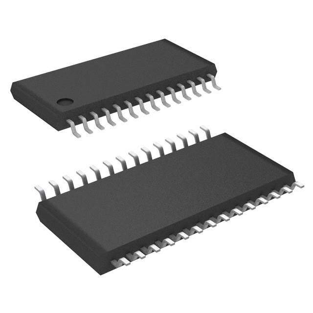
| 供应商器件封装 | 28-TSSOP |
| 其它名称 | ADM10751ARUZ |
| 内部开关 | 无 |
| 功能引脚 | - |
| 包装 | 管件 |
| 可编程特性 | 断路器,限流,故障超时,OVP,UVLO |
| 商标 | Analog Devices |
| 安装类型 | 表面贴装 |
| 安装风格 | SMD/SMT |
| 封装 | Tube |
| 封装/外壳 | 28-TSSOP(0.173",4.40mm 宽) |
| 封装/箱体 | TSSOP |
| 工作温度 | -40°C ~ 85°C |
| 工厂包装数量 | 50 |
| 应用 | -48V |
| 标准包装 | 50 |
| 特性 | 自动重试,PMBus |
| 电压-电源 | -80 V ~ -35 V |
| 电流-电源 | 5.5mA |
| 电流-输出(最大值) | - |
| 电源电压-最大 | - 35 V |
| 电源电压-最小 | - 80 V |
| 类型 | 热交换控制器, 监控器 |
| 系列 | ADM1075 |
| 通道数 | 1 |
| 通道数量 | 1 Channel |
| 配用 | /product-detail/zh/EVAL-ADM1075MEBZ/EVAL-ADM1075MEBZ-ND/4915062 |


- 商务部:美国ITC正式对集成电路等产品启动337调查
- 曝三星4nm工艺存在良率问题 高通将骁龙8 Gen1或转产台积电
- 太阳诱电将投资9.5亿元在常州建新厂生产MLCC 预计2023年完工
- 英特尔发布欧洲新工厂建设计划 深化IDM 2.0 战略
- 台积电先进制程称霸业界 有大客户加持明年业绩稳了
- 达到5530亿美元!SIA预计今年全球半导体销售额将创下新高
- 英特尔拟将自动驾驶子公司Mobileye上市 估值或超500亿美元
- 三星加码芯片和SET,合并消费电子和移动部门,撤换高东真等 CEO
- 三星电子宣布重大人事变动 还合并消费电子和移动部门
- 海关总署:前11个月进口集成电路产品价值2.52万亿元 增长14.8%


PDF Datasheet 数据手册内容提取
−48 V Hot Swap Controller and Digital Power Monitor with PMBus Interface Data Sheet ADM1075 FEATURES PRODUCT HIGHLIGHTS Constant power foldback for FET SOA protection 1. Constant Power Foldback. Precision (<1.0%) current and voltage measurement Maximum FET power set by a PLIM resistor divider. This Controls inrush and faults for negative supply voltages eases complexity when designing to maintain FET SOA. Suitable for wide input range due to internal shunt regulator 2. Adjustable Current Limit. 25 mV/50 mV full-scale sense voltage The current limit is adjustable via the ISET pin allowing for Fine tune current limit to allow use of standard sense resistor the use of a standard value sense resistor. Soft start inrush current limit profiling 3. 12-Bit ADC. 1% accurate UVH and OV pins, 1.5% accurate UVL pin Accurate voltage, current, and power measurements. Also PMBus/I2C interface for control, telemetry, and fault enables calculation of energy consumption over time. recording 4. PMBus/I2C Interface. 28-lead LFCSP and TSSOP PMBus fast mode compliant interface used to read back −40°C to 105°C junction temperature (T) operating range J status and data registers and set warning and fault limits. APPLICATIONS 5. Fault Recording. Telecommunication and data communication equipment Latched status registers provide useful debugging infor- Central office switching mation to help trace faults in high reliability systems. −48 V distributed power systems 6. Built-In Soft Start. Negative power supply control Soft start capacitor controls inrush current profile with High availability servers di/dt control. FUNCTIONAL BLOCK DIAGRAM –48V RTN (0V) 12V RDROP VIN SPLYGD SHDN RESTART 5V 3.3V VEEUVH GREEVNFCEECRR AEANNTDCOER ACCPPUOOMWWUEELRARTOR DIAGNITDAL GLGSADPPTAOOCO21H//AALLEERRTT21/CONV CLOAD CDOCN-VTEOR-DTCER 2.G...N8eVtDc. UVL UNDERAVNODLTAGE MULTIPLIER PMBUS SSDCALI OVERVOLTAGE OV DETECTOR 12-BIT ADC ADR ADC_AUX ADC_V FET POWER PWRGD FOLDBACK DRAIN CONTROL PLIM VCAP SDA_ISO FAULT TIMER VEE ADuM1250 SCL_ISO ISET N-FET GATE CONTROL GATE CURRENT LIMIT SENSE+ RSENSE SENSE– TIMER SS VEE_G VEE –48V 09312-001 Figure 1. Rev. D Document Feedback Information furnished by Analog Devices is believed to be accurate and reliable. However, no responsibility is assumed by Analog Devices for its use, nor for any infringements of patents or other One Technology Way, P.O. Box 9106, Norwood, MA 02062-9106, U.S.A. rights of third parties that may result from its use. Specifications subject to change without notice. No license is granted by implication or otherwise under any patent or patent rights of Analog Devices. Tel: 781.329.4700 ©2011–2018 Analog Devices, Inc. All rights reserved. Trademarks and registered trademarks are the property of their respective owners. Technical Support www.analog.com
ADM1075 Data Sheet TABLE OF CONTENTS Features .............................................................................................. 1 Group Commands ..................................................................... 30 Applications ....................................................................................... 1 Hot Swap Control Commands ................................................. 31 Product Highlights ........................................................................... 1 ADM1075 Information Commands ........................................ 31 Functional Block Diagram .............................................................. 1 Status Commands ...................................................................... 31 Revision History ............................................................................... 3 GPO and Alert Pin Setup Commands..................................... 32 General Description ......................................................................... 4 Power Monitor Commands ...................................................... 32 Specifications ..................................................................................... 5 Warning Limit Setup Commands ............................................ 33 Serial Bus Timing ......................................................................... 9 PMBus Direct Format Conversion .......................................... 34 Absolute Maximum Ratings .......................................................... 10 Voltage and Current Conversion Using LSB Values .............. 35 Thermal Resistance .................................................................... 10 ADM1075 Alert Pin Behavior ...................................................... 36 ESD Caution ................................................................................ 10 Faults and Warnings .................................................................. 36 Pin Configuration and Function Description ............................ 11 Generating an Alert ................................................................... 36 Typical Performance Characteristics ........................................... 13 Handling/Clearing an Alert ...................................................... 36 Theory of Operation ...................................................................... 20 SMBus Alert Response Address ............................................... 37 Powering the ADM1075 ............................................................ 20 Example Use of SMBus Alert Response Address ................... 37 Current Sense Inputs .................................................................. 21 Digital Comparator Mode ......................................................... 37 Current Limit Reference ............................................................ 21 PMBus Command Reference........................................................ 38 Setting the Current Limit (ISET).............................................. 22 Register Details ............................................................................... 39 Soft Start ...................................................................................... 22 Operation Command Register ................................................. 39 Constant Power Foldback (PLIM) ........................................... 22 Clear Faults Register .................................................................. 39 TIMER ......................................................................................... 23 PMBus Capability Register ....................................................... 39 Setting a Linear Output Voltage Ramp at Power-Up ............. 24 IOUT OC Warn Limit Register ................................................ 39 Hot Swap Fault Retry ................................................................. 25 VIN OV Warn Limit Register ................................................... 39 Fast Response to Severe Overcurrent ...................................... 25 VIN UV Warn Limit Register ................................................... 39 UV and OV ................................................................................. 25 PIN OP Warn Limit Register .................................................... 40 PWRGD ....................................................................................... 25 Status Byte Register .................................................................... 40 DRAIN ......................................................................................... 26 Status Word Register .................................................................. 40 SPLYGD ....................................................................................... 26 IOUT Status Register ................................................................. 41 LATCH ......................................................................................... 26 Input Status Register .................................................................. 41 SHDN ........................................................................................... 26 Manufacturing Specific Status Register ................................... 42 RESTART ..................................................................................... 26 Read EIN Register ...................................................................... 43 Read VIN Register...................................................................... 43 FET Health .................................................................................. 26 Read IOUT Register ................................................................... 43 Power Monitor ............................................................................ 26 Read PIN Register ...................................................................... 43 Isolation ....................................................................................... 27 PMBus Revision Register .......................................................... 43 PMBus Interface ............................................................................. 28 Manufacturing ID Register ....................................................... 44 Device Addressing ...................................................................... 28 Manufacturing Model Register ................................................ 44 SMBus Protocol Usage ............................................................... 28 Manufacturing Revision Register ............................................. 44 Packet Error Checking ............................................................... 28 Peak IOUT Register ................................................................... 44 Partial Transactions on I2C Bus ................................................ 28 Peak VIN Register ...................................................................... 45 SMBus Message Formats ........................................................... 29 Rev. D | Page 2 of 52
Data Sheet ADM1075 Peak VAUX Register ................................................................... 45 Read PIN_EXT Register............................................................. 49 Power Monitor Control Register ............................................... 45 Read EIN_EXT Register............................................................. 49 Power Monitor Configuration Register ................................... 45 Read VAUX Register ................................................................... 50 ALERT1 Configuration Register ............................................... 46 VAUX OV Warn Limit Register ................................................ 50 ALERT2 Configuration Register ............................................... 47 VAUX UV Warn Limit Register ................................................ 50 IOUT WARN2 Limit Register ................................................... 48 VAUX Status Register ................................................................. 50 Device Configuration Register .................................................. 48 Outline Dimensions ........................................................................ 51 Power Cycle Register .................................................................. 49 Ordering Guide ........................................................................... 52 Peak PIN Register........................................................................ 49 REVISION HISTORY 1/2018—Rev. C to Rev. D 3/2012—Rev. 0 to Rev. A Changed CP-28-6 to CP-28-10 ............................................. Throughout Added 28-Lead LFCSP ...................................................... Universal Changes to Operation Command Register Section and Table 9 .... 39 Changes to Features Section and Product Highlights Section .... 1 Changes to Device Configuration Register Section and Table 36 .. 49 Changes to ADC Conversion Time comments in Table 1 .......... 8 Updated Outline Dimensions ........................................................ 51 Changes to Table 4 .......................................................................... 10 Changes to Ordering Guide ........................................................... 52 Added Figure 4; Renumbered Sequentially; and changes to Table 5 ............................................................................................... 11 4/2014—Rev. B to Rev. C Changes to Current Limit Reference Section .............................. 21 Added Setting a Linear Output Voltage Ramp at Power-Up Changes to Voltage and Current Conversion Using LSB Section and Figure 51; Renumbered Sequentially ...................... 24 Values Section .................................................................................. 35 Changes to Table 8 .......................................................................... 38 4/2013—Rev. A to Rev. B Changes to Table 20 ........................................................................ 43 Changes to Figure 4......................................................................... 11 Changes to Table 25 through Table 27 ......................................... 44 Changes to Figure 43 ...................................................................... 21 Changes to Table 32 ........................................................................ 45 Added I Partial Transactions on I2C Bus Section ....................... 28 Changes to Table 38 and Table 39 ................................................. 49 Change to Bit 14, Table 16 .............................................................. 40 Changes to Outline Dimensions and Ordering Guide .............. 51 Changes to Table 32 ........................................................................ 45 Change to Bits[1:0], Table 36 ......................................................... 49 10/2011—Revision 0: Initial Version Rev. D | Page 3 of 52
ADM1075 Data Sheet GENERAL DESCRIPTION The ADM1075 is a full feature, negative voltage, hot swap control- The ADM1075 has separate UVx and OV pins for undervoltage ler with constant power foldback and high accuracy digital current and overvoltage detection. The FET is turned off if a nontransient and voltage measurement that allows boards to be safely inserted voltage less than the undervoltage threshold (typically −35 V) is and removed from a live −48 V backplane. The part provides detected on the UVx pins or if greater than the overvoltage precise and robust current limiting and protection against both threshold (typically −80 V) is detected on the OV pin. The transient and nontransient short circuits and overvoltage and operating voltage range of the ADM1075 is programmable via undervoltage conditions. The ADM1075 typically operates from resistor networks on the UVx and OV pins. The hysteresis levels a negative voltage of −35 V to −80 V and, due to shunt regulation, on the overvoltage detectors can also be altered by selecting the has excellent voltage transient immunity. The operating range of appropriate resistors. There are two separate UVx pins to allow the part is flexible due to the shunt regulator, and the part can be accurate programming of hysteresis. powered directly by a 10 V rail to save shunt power dissipation In the case of a short circuit, the ADM1075 has a fast response (see the Powering the ADM1075 section for more details). circuit to detect and respond adequately to this event. If the A full-scale current limit of 25 mV or 50 mV can be selected by sense voltage exceeds 1.5 times the normal current limit, a high choosing the appropriate model. The maximum current limit is current (750 mA minimum) gate pull-down switch is activated set by the combination of the sense resistor, R , and the input to shut down the MOSFET as quickly as possible. There is a SENSE voltage on the ISET pin, using external resistors. This allows fine default internal glitch filter of 900 ns. If a longer filter time or tuning of the trip voltage so that standard sense resistors can be different severe overcurrent limit is required, these parameters used. Inrush current is limited to this programmable value by can be adjusted via the PMBus™ interface. controlling the gate drive of an external N-channel FET. A built- The ADM1075 also includes a 12-bit ADC to provide digital in soft start function allows control of the inrush current profile by measurement of the voltage and load current. The current is an external capacitor on the soft start (SS) pin. measured at the output of the internal current sense amplifier An external capacitor on the TIMER pin determines the maxi- and the voltage from the ADC_V input. This data can be read mum allowed on-time for when the system is in current limit. across the PMBus interface. This is based on the safe operating area (SOA) limits of the The PMBus interface allows a controller to read current, voltage, MOSFET. A constant power foldback scheme is used to control and power measurements from the ADC. Measurements can be the power dissipation in the MOSFET during power-up and initiated by a PMBus command or can be set up to run continu- fault conditions. The ADM1075 regulates the current dynami- ously. The user can read the latest conversion data whenever it cally to ensure that the power in the MOSFET is within SOA is required. A power accumulator is also provided to report limits as V changes. After the timer has expired, the device DS total power consumed in a user specified period (total energy). shuts down the MOSFET. The level of this power, along with Up to four unique I2C addresses can be created, depending on the TIMER regulation time, can be set to ensure that the the configuration of the ADR pin. MOSFET remains within the SOA limits. The GPO1/ALERT1/CONV and GPO2/ALERT2 outputs can The ADM1075 employs a limited consecutive retry scheme be used as a flag to warn a microcontroller or FPGA of one or when the LATCH pin is tied to the SHDN pin. In this mode, more fault/warning conditions becoming active. The fault type if the load current reaches the limit, the FET gate is pulled low and level is programmed across the PMBus, and the user can after the timer expires and retries after a cooling period for select which faults/warnings activate the alert. seven attempts only. If the fault remains, the device latches off, Other functions include and the MOSFET is disabled until a manual restart is initiated. Alternatively, the ADM1075 can be set to retry only once by • PWRGD output, which can be used to enable a power isolating the LATCH pin from the SHDN pin. The part can module (the DRAIN and GATE pins are monitored to also be configured to retry an infinite number of times with a determine when the load capacitance is fully charged) 10 second interval between restarts by connecting the GPO2 • SHDN input to manually disable the GATE drive pin to the RESTART pin. • RESTART input to remotely initiate a 10 second shutdown Rev. D | Page 4 of 52
Data Sheet ADM1075 SPECIFICATIONS VEE = −48 V, V = (V − V ) = 0 mV, shunt regulation current = 10 mA, T = −40°C to +105°C, unless otherwise noted. SENSE SENSE+ SENSE− J Table 1. Parameter Min Typ Max Unit Test Conditions/Comments SYSTEM SUPPLY Voltage Transient Immunity −200 V Typical Operating Voltage −80 −35 V Determined by external component, R SHUNT SHUNT REGULATOR Operating Supply Voltage Range, VIN 11.5 12.3 13 V Shunt regulation voltage, I = 5.5 mA to 30 mA, IN maximum I dependent on T, θ (see the Powering the IN A JA ADM1075 section) Quiescent Supply Current 5.5 mA VIN = 13 V Undervoltage Lockout, V 9.2 V UVLO_RISING Undervoltage Lockout Hysteresis 600 mV Power Directly Without Shunt 9.2 11.5 V UV PINS—UNDERVOLTAGE DETECTION Undervoltage Rising Threshold, V 0.99 1.0 1.01 V UVH Undervoltage Falling Threshold, V 0.887 0.9 0.913 V UVL Total Undervoltage Hysteresis 100 mV When UVL and UVH are tied together Undervoltage Fault Filter 3.5 7.5 µs UV Propagation Delay 5 8 µs UV low to GATE pull-down active UVL/UVH Input Current 1 50 nA OV PIN—OVERVOLTAGE DETECTION Overvoltage Rising Threshold, V 0.99 1.0 1.01 V OVR Overvoltage Hysteresis Current 4.3 5 5.7 µA Overvoltage Fault Filter 1.75 3.75 µs OV Propagation Delay 2 4 µs OV high to GATE pull-down active OV Input Current 1 50 nA GATE PIN Gate Voltage High 11 12 13 V I = −1.0 µA GATE Gate Voltage Low 10 100 mV I = 100 µA GATE Pull-Up Current −50 −30 µA V = 0 V to 8 V; V = 2 V GATE SS Pull-Down Current (Regulation) 100 µA V ≥ 2 V GATE Pull-Down Current (UV/OV/OC) 5 10 mA V ≥ 2 V GATE Pull-Down Current (Severe OC) 750 1500 2000 mA V ≥ 6 V GATE Pull-Down On-Time (Severe OC) 8 16 µs Gate Hold-Off Resistance 20 Ω 0 V ≤ VIN ≤ 9.2 V SENSE+, SENSE− SENSE+, SENSE− Input Current, I 100 μA V ≤ 65 mV for ADM1075-1, per individual pin; SENSEx SENSE V ≤ 130 mV for ADM1075-2, per individual pin SENSE SENSE+, SENSE− Input Imbalance, I 1 μA I = I − I ΔSENSEx ΔSENSEx SENSE+ SENSE− VCAP Internally Regulated Voltage, V 2.66 2.7 2.74 V 0 ≤ I ≤ 100 μA; C = 1 μF VCAP VCAP VCAP ISET ISET Reference Select Threshold, V 1.35 1.5 1.65 V If V > V an internal 1 V reference (V ) is used ISETRSTH ISET ISETRSTH CLREF ISET Internal Reference, V 1 V Accuracies included in total sense voltage accuracies CLREF Gain of Current Sense Amplifier, AV 50/25 V/V Accuracies included in total sense voltage accuracies CSAMP ISET Input Current, I 100 nA V ≤ VCAP ISET ISET ADM1075-1 ONLY (GAIN = 50) Hot Swap Sense Voltage Hot Swap Sense Voltage Current Limit, 19.4 20 20.6 mV V > 1.65 V; V = 3 V; I = 0 μA; V ≥ 2 V; V = 0 V ISET GATE GATE SS PLIM V SENSECL 24.5 25 25.5 mV V = 1.25 V; V = 3 V; I = 0 μA; V ≥ 2 V; V = 0 V ISET GATE GATE SS PLIM 19.5 20 20.5 mV V = 1.0 V; V = 3 V; I = 0 μA; V ≥ 2 V; V = 0 V ISET GATE GATE SS PLIM 14.5 15 15.5 mV V = 0.75 V; V = 3 V; I = 0 μA; V ≥ 2 V; V = 0 V ISET GATE GATE SS PLIM Rev. D | Page 5 of 52
ADM1075 Data Sheet Parameter Min Typ Max Unit Test Conditions/Comments Constant Power Active 9.4 10 11.0 mV V > 1.65 V; V = 3 V; I = 0 μA; V ≥ 2 V; V = 0.2 V ISET GATE GATE SS PLIM 4.5 5 5.7 mV V > 1.65 V; V = 3 V; I = 0 μA; V ≥ 2 V; V = 0.4 V ISET GATE GATE SS PLIM 1.4 2 2.6 mV V > 1.65 V; V = 3 V; I = 0 μA; V ≥ 2 V; V = 1.2 V ISET GATE GATE SS PLIM Circuit Breaker Offset, V 0.6 0.75 0.95 mV Circuit breaker voltage, V = V − V CBOS CB SENSECL CBOS Severe Overcurrent Activates high current gate pull-down Voltage Threshold, V 23 25 27 mV V > 1.65 V; V ≥ 2 V; optional select through PMBus SENSEOC ISET SS 28 30 32 mV V > 1.65 V; V ≥ 2 V; default at power-up ISET SS 38 40 42 mV V > 1.65 V; V ≥ 2 V; optional select through PMBus ISET SS 43 45 47 mV V > 1.65 V; V ≥ 2 V; optional select through PMBus ISET SS Response Time Glitch Filter Duration 50 200 ns V > 1.65 V; V ≥ 2 V; V step from 18 mV to 52 mV; ISET SS SENSE optional select through PMBus 500 900 ns V > 1.65 V; V ≥ 2 V; V step from 18 mV to 52 mV; ISET SS SENSE default at power-up 6.2 10.7 µs V > 1.65 V; V ≥ 2 V; V step from 18 mV to 52 mV; ISET SS SENSE optional select through PMBus 44 57 µs V > 1.65 V; V ≥ 2 V; V step from 18 mV to 52 mV; ISET SS SENSE optional select through PMBus Total Response Time 180 300 ns V > 1.65 V; V ≥ 2 V; V step from 18 mV to 52 mV; ISET SS SENSE optional select through PMBus 610 950 ns V > 1.65 V; V ≥ 2 V; V step from 18 mV to 52 mV; ISET SS SENSE default at power-up 7 13 µs VISET > 1.65 V; VSS ≥ 2 V; VSENSE step from 18 mV to 52 mV; optional select through PMBus 45 60 µs V > 1.65 V; V ≥ 2 V; V step from 18 mV to 52 mV; ISET SS SENSE optional select through PMBus ADM1075-2 ONLY (GAIN = 25) Hot Swap Sense Voltage Hot Swap Sense Voltage Current Limit, 39.2 40 40.8 mV V > 1.65 V; V = 3 V; I = 0 μA; V ≥ 2 V; V = 0 V ISET GATE GATE SS PLIM V SENSECL 49.2 50 50.8 mV V = 1.25 V; V = 3 V; I = 0 μA; V ≥ 2 V; V = 0 V ISET GATE GATE SS PLIM 39.2 40 40.8 mV V = 1.0 V; V = 3 V; I = 0 μA; V ≥ 2 V; V = 0 V ISET GATE GATE SS PLIM 29.2 30 30.8 mV V = 0.75 V; V = 3 V; I = 0 μA; V ≥ 2 V; V = 0 V ISET GATE GATE SS PLIM Constant Power Active 19 20 21.9 mV V > 1.65 V; V = 3 V; I = 0 μA; V ≥ 2 V; V = 0.2 V ISET GATE GATE SS PLIM 9.2 10 11.2 mV V > 1.65 V; V = 3 V; I = 0 μA; V ≥ 2 V; V = 0.4 V ISET GATE GATE SS PLIM 3 4 5.0 mV V > 1.65 V; V = 3 V; I = 0 μA; V ≥ 2 V; V = 1.2 V ISET GATE GATE SS PLIM Circuit Breaker Offset, V 1.1 1.5 1.9 mV Circuit breaker voltage, V = V − V CBOS CB SENSECL CBOS Severe Overcurrent Activates high current gate pull-down Voltage Threshold, V 46 50 54 mV V > 1.65 V; V ≥ 2 V; optional select through PMBus SENSEOC1 ISET SS 56 60 64 mV V > 1.65 V; V ≥ 2 V; default at power-up ISET SS 76 80 84 mV V > 1.65 V; V ≥ 2 V; optional select through PMBus ISET SS 86 90 94 mV V > 1.65 V; V ≥ 2 V; optional select through PMBus ISET SS Response Time Glitch Filter Duration 50 200 ns V > 1.65 V; V ≥ 2 V; V step from 36 mV to 104 mV; ISET SS SENSE optional select through PMBus 400 900 ns V > 1.65 V; V ≥ 2 V; V step from 36 mV to 104 mV; ISET SS SENSE default at power-up 6.2 10.7 µs V > 1.65 V; V ≥ 2 V; V step from 36 mV to 104 mV; ISET SS SENSE optional select through PMBus 44 57 µs V > 1.65 V; V ≥ 2 V; V step from 36 mV to 104 mV; ISET SS SENSE optional select through PMBus Rev. D | Page 6 of 52
Data Sheet ADM1075 Parameter Min Typ Max Unit Test Conditions/Comments Total Response Time 180 300 ns V > 1.65 V; V ≥ 2 V; V step from 36 mV to 104 mV; ISET SS SENSE optional select through PMBus 610 950 ns V > 1.65 V; V ≥ 2 V; V step from 36 mV to 104 mV; ISET SS SENSE default at power-up 7 13 µs VISET > 1.65 V; VSS ≥ 2 V; VSENSE step from 36 mV to 104 mV; optional select through PMBus 45 60 µs V > 1.65 V; V ≥ 2 V; V step from 36 mV to 104 mV; ISET SS SENSE optional select through PMBus SOFT START SS Pull-Up Current, I −11.5 −10 −8.5 µA V = 0V SS SS Default V Limit 0.6 1.25 1.9 mV When V reaches this level, I is enabled, ramping; SENSECL SENSE SS V = 0 V; ADM1075-1 only (gain = 50) SS 1.2 2.5 3.8 mV When V reaches this level, I is enabled, ramping; SENSE SS V = 0 V; ADM1075-2 only (gain = 25) SS SS Pull-Down Current 100 µA V = 1 V SS TIMER Timer Pull-Up Current (POR), I −4 −3 −2 µA Initial power-on reset; V = 0.5 V TIMERUPPOR TIMER Timer Pull-Up Current (OC Fault), I −63 −60 −57 µA Overcurrent fault; 0.05 V ≤ V ≤ 1 V TIMERUPFLT TIMER Timer Pull-Down Current (Retry), I 1.7 2 2.3 µA After a fault when GATE is off; V = 0.5 V TIMERDNRT TIMER Timer Retry/OC Fault Current Ratio 3.33 % Defines the limits of the autoretry duty cycle Timer Pull-Down Current (Hold), I 100 µA Holds TIMER at 0 V when inactive; V = 0.5 V TIMERDNHOLD TIMER Timer High Threshold, V 0.98 1.0 1.02 V TIMERH Timer Low Threshold, V 0.03 0.05 0.07 V TIMERL PLIM PLIM Active Threshold 0.08 0.09 0.1 V V > 1.65 V ISET Input Current, I 100 nA V ≤ 1 V PLIM PLIM Minimum Current Clamp, V 75 100 125 mV V = 1.2 V; V = (V ÷ gain) = minimum ICLAMP PLIM SENSE_IMIN ICLAMP allowed current control DRAIN DRAIN Voltage at Which PWRGD Asserts 1.9 2 2.1 V IDRAIN ≤ 50 µA ADC_AUX/ADC_V Input Current 100 nA 0 V ≤ V ≤ 1.5 V ADC SHDN PIN Input High Voltage, V 1.1 V IH Input Low Voltage, V 0.8 V IL Glitch Filter 1 µs Internal Pull-Up Current 8 µA Pull-up to VIN RESTART PIN Input High Voltage, V 1.1 V IH Input Low Voltage, V 0.8 V IL Glitch Filter 1 µs Internal Pull-Up Current 8 µA Pull-up to VIN SPLYGD PIN Output Low Voltage, V 0.4 V I = 1 mA OL_LATCH SPLYGD 1.5 V I = 5 mA SPLYGD Leakage Current 100 nA V ≤ 2 V; SPLYGD pin disabled SPLYGD 1 µA V ≤ 14 V; SPLYGD pin disabled SPLYGD LATCH PIN Output Low Voltage, V 0.4 V I = 1 mA OL_LATCH LATCH 1.5 V I = 5 mA LATCH Leakage Current 100 nA V ≤ 2 V; LATCH pin disabled LATCH 1 µA V ≤ 14 V; LATCH pin disabled LATCH GPO1/ALERT1/CONV PIN Output Low Voltage, V 0.4 V I = 1 mA OL_GPO1 GPO 1.5 V I = 5 mA GPO Rev. D | Page 7 of 52
ADM1075 Data Sheet Parameter Min Typ Max Unit Test Conditions/Comments Leakage Current 100 nA V ≤ 2 V; GPO disabled GPO 1 µA V = 14 V; GPO disabled GPO Input High Voltage, V 1.1 V Configured as CONV pin IH Input Low Voltage, V 0.8 V Configured as CONV pin IL Glitch Filter 1 µs Configured as CONV pin GPO2/ALERT2 PIN Output Low Voltage, V 0.4 V I = 1 mA OL_GPO2 GPO 1.5 V I = 5 mA GPO Leakage Current 100 nA V ≤ 2 V; GPO disabled GPO 1 µA V = 14 V; GPO disabled GPO PWRGD PIN Output Low Voltage, V 0.4 V I = 1 mA OL_PWRGD PWRGD 1.5 V I = 5 mA PWRGD VIN That Guarantees Valid Output 1 V I = 100 μA; V = 0.4 V SINK OL_PWRGD Leakage Current 100 nA V ≤ 2 V; PWRGD active PWRGD 1 µA V = 14 V; PWRGD active PWRGD CURRENT AND VOLTAGE MONITORING Current Sense Absolute Error (ADM1075-1) 25 mV input range; 128 sample averaging (unless otherwise noted) −0.01 ±0.7 % V = 25 mV SENSE 0.05 ±0.85 % V = 20 mV SENSE 0.07 ±0.85 % V = 20 mV; 16 sample averaging SENSE 0.04 ±2.8 % V = 20 mV; 1 sample averaging SENSE ±1.0 % V = 15 mV SENSE ±1.4 % V = 10 mV SENSE ±2.7 % V = 5 mV SENSE ±5.9 % V = 2.5 mV SENSE Current Sense Absolute Error (ADM1075-2) 50 mV input range; 128 sample averaging (unless otherwise noted) −0.03 ±0.65 % V = 50 mV SENSE −0.03 ±0.7 % V = 40 mV SENSE −0.03 ±0.7 % V = 40 mV; 16 sample averaging SENSE −0.04 ±1.35 % V = 40 mV; 1 sample averaging SENSE ±0.75 % V = 30 mV SENSE ±0.9 % V = 20 mV SENSE ±1.7 % V = 10 mV SENSE ±3.0 % V = 5 mV SENSE ADC_V/ADC_AUX Absolute Accuracy −0.8 +0.8 % 0.6 V ≤ V ≤ 1.5 V ADC ADC Conversion Time 1 sample of voltage and current; from command received to valid data in register 191 219 µs VAUX disabled 263 301 µs VAUX enabled 16 samples of voltage and current averaged; from command received to valid data in register 2.830 3.243 ms VAUX disabled 3.987 4.568 ms VAUX enabled 128 samples of voltage and current averaged; from command received to valid data in register 22.54 25.83 ms VAUX disabled (default on power-up) 31.79 36.43 ms VAUX enabled Power Multiplication Time 14 µs Rev. D | Page 8 of 52
Data Sheet ADM1075 Parameter Min Typ Max Unit Test Conditions/Comments ADR PIN See Table 6 Address Set to 00 0 0.8 V Connect to VEE Input Current for Address 00 −40 −22 μA V = 0 V to 0.8 V ADR Address Set to 01 135 150 165 kΩ Resistor to VEE Address Set to 10 −1 +1 μA No connect state; maximum leakage current allowed Address Set to 11 2.1 V Connect to VCAP Input Current for Address 11 3 10 μA V = 2.0 V to VCAP; must not exceed the maximum ADR allowable current draw from VCAP SERIAL BUS DIGITAL INPUTS (SDAI/SDAO, SCL) Input High Voltage, V 1.1 V IH Input Low Voltage, V 0.8 V IL Output Low Voltage, V 0.4 V I = 4 mA, SDAO only OL OL Input Leakage, I −10 +10 μA LEAK-PIN −5 +5 μA Device is not powered Nominal Bus Voltage, V 2.7 5.5 V 3 V to 5 V ±10% DD Capacitive Load per Bus Segment, C 400 pF BUS Capacitance for SDAI, SDAO, or SCL Pin, C 5 pF PIN Input Glitch Filter, t 0 50 ns SP SERIAL BUS TIMING Table 2. Parameter Description Min Typ Max Unit Test Conditions/Comments f Clock frequency 400 kHz SCLK t Bus free time 1.3 μs BUF t Start hold time 0.6 μs HD;STA t Start setup time 0.6 μs SU;STA t Stop setup time 0.6 μs SU;STO t SDA1 hold time 300 900 ns HD;DAT t SDA1 setup time 100 ns SU;DAT t SCL low time 1.3 μs LOW t SCL high time 0.6 μs HIGH t2 SCL, SDA1 rise time 20 300 ns R t SCL, SDA1 fall time 20 300 ns F t SCL, SDA1 output fall time 20 + 0.1 × C 250 ns OF BUS 1 SDAI and SDAO tied together. 2 tR = (VIL(MAX) – 0.15) to (VIH3V3 + 0.15) and tF = 0.9 VDD to (VIL(MAX) – 0.15); where VIH3V3 = 2.1 V, and VDD = 3.3 V. t LOW t t R F VIH SCL VIL t t SU;STA SU;STO tHD;DAT tHIGH tSU;DAT t HD;STA VIH SDA VIL P tBUF S S P 09312-002 Figure 2. Serial Bus Timing Diagram Rev. D | Page 9 of 52
ADM1075 Data Sheet ABSOLUTE MAXIMUM RATINGS Table 3. Stresses at or above those listed under Absolute Maximum Parameter Rating Ratings may cause permanent damage to the product. This is a VIN Pin to VEE −0.3 V to +14 V stress rating only; functional operation of the product at these UVL Pin to VEE −0.3 V to +4 V or any other conditions above those indicated in the operational UVH Pin to VEE −0.3 V to +4 V section of this specification is not implied. Operation beyond OV Pin to VEE −0.3 V to +4 V the maximum operating conditions for extended periods may ADC_V Pin to VEE −0.3 V to +4 V affect product reliability. ADC_AUX Pin to VEE −0.3 V to +4 V THERMAL RESISTANCE SS Pin to VEE −0.3 V to (VCAP + 0.3 V) θ is specified for the worst-case conditions, that is, a device TIMER Pin to VEE −0.3 V to (VCAP + 0.3 V) JA soldered in a circuit board for surface-mount packages. VCAP Pin to VEE −0.3 V to +4 V ISET Pin to VEE −0.3 V to +4 V Table 4. Thermal Resistance SPLYGD Pin to VEE −0.3 V to +18 V Package Type θ 1 θ Unit JA JC LATCH Pin to VEE −0.3 V to +18 V 28-Lead TSSOP 68 20 °C/W RESTART Pin to VEE −0.3 V to +18 V 28-Lead LFCSP 35 4 °C/W SHDN Pin to VEE −0.3 V to +18 V 1 Measured on JEDEC 4-layer board in still air. PWRGD Pin to VEE −0.3 V to +18 V ESD CAUTION DRAIN Pin to VEE −0.3 V to (VCAP + 0.3 V) SCL Pin to VEE −0.3 V to +6.5 V SDAI Pin to VEE −0.3 V to +6.5 V SDAO Pin to VEE −0.3 V to +6.5 V ADR Pin to VEE −0.3 V to (VCAP + 0.3 V) GPO1/ALERT1/CONV Pin to VEE −0.3 V to +18 V GPO2/ALERT2 Pin to VEE −0.3 V to +18 V PLIM Pin to VEE −0.3 V to +4 V GATE Pin to VEE −0.3 V to +18 V SENSE+ Pin to VEE −0.3 V to +4 V SENSE− Pin to VEE −0.3 V to +0.3 V VEE to VEE_G −0.3 V to +0.3 V Continuous Current into Any Pin ±10 mA Storage Temperature Range −65°C to +125°C Operating Junction Temperature −40°C to +105°C Range Lead Temperature, Soldering (10 sec) 300°C Junction Temperature 150°C Rev. D | Page 10 of 52
Data Sheet ADM1075 PIN CONFIGURATION AND FUNCTION DESCRIPTION + UVL UVH VNI DRANIVEE_G GATE NSESE 8 7 6 54 3 2 2 2 2 22 2 2 OV 1 21SENSE– PLIM 2 20VEE VCAP 3 19SPLYGD ADM1075 ADC_V 4 18ADC_AUX DRAIN 1 28 VEE_G TOP VIEW ISET 5 (Not to Scale) 17PWRGD VIN 2 27 GATE SS 6 16SCL UVH 3 26 SENSE+ TIMER 7 15SDAI UVL 4 25 SENSE– OV 5 ADM1075 24 VEE 89 10 11 12 13 14 PLIM 6 TOP VIEW 23 SPLYGD HR N T V 2 O AVDICCSAS_EVSPT 17890 (Not to Scale) 22122190 PSSAWCDDALCRI_GADUX LATCDA SHD RRESTA O1ALERT1CN// GOP2ALERT/ SDA TIMER 11 18 SDAO PO G LATCH 12 17 GPO2/ALERT2 NOTES SAHDDRN 1134Figure 3. TSSOP P11in65 CGRoEPnSOfiT1gA/uARrLTaEtRioTn1/ CONV 09312-004 1 . EICMXOPPNRONOSEVECEDT TEPHDAEDTR.O MS VOAELLE DD.EISRS TIPHAET EIOXNP.O TSHEED EPXAPDOTSOE DTHPAED B COAANR DBETO 09312-003 Figure 4. LFCSP Pin Configuration Table 5. Pin Function Descriptions Pin No. TSSOP LFCSP Mnemonic Description 1 25 DRAIN Connect to the drain pin of the FET through a resistor. The current in this resistor is used to determine the V of the MOSFET. This is used for PWRGD. DS 2 26 VIN Shunt Regulated Positive Supply to Chip. Connect to the positive supply rail via a shunt resistor. A 1 μF capacitor to VEE is recommended on the VIN pin. 3 27 UVH Undervoltage Rising Input Pin. An external resistor divider is used from the supply to this pin to allow an internal comparator to detect if the supply is under the UVH limit. 4 28 UVL Undervoltage Falling Input Pin. An external resistor divider is used from the supply to this pin to allow an internal comparator to detect if the supply is under the UVL limit. 5 1 OV Overvoltage Input Pin. An external resistor divider is used from the supply to this pin to allow an internal comparator to detect if the supply is above the OV limit. 6 2 PLIM The voltage on this pin is proportional to the V voltage of the FET. As the PLIM voltage changes, the DS current limit automatically adjusts to maintain constant power across the FET. 7 3 VCAP A capacitor with a value of 1 μF or greater should be placed on this pin to maintain good accuracy. This is an internal regulated supply. This pin can be used as a reference to program the ISET pin voltage. 8 4 ADC_V This pin is used to read back the input voltage using the internal ADC. It can be connected to the OV string or a separate divider. 9 5 ISET This pin allows the current limit threshold to be programmed. The default limit is set when this pin is connected directly to VCAP. Alternatively, using a resistor divider from VCAP, the current limit can be adjusted to achieve a user defined sense voltage. An external reference can also be used. 10 6 SS A capacitor is used on this pin to set the inrush current soft start ramp profile. The voltage on the soft start pin controls the current sense voltage limit, allowing control over the inrush current profile. 11 7 TIMER Timer Pin. An external capacitor, C , sets an initial timing cycle delay and a fault delay. The GATE TIMER pin turns off when the voltage on the TIMER pin exceeds the upper threshold. 12 8 LATCH This pin signals the device latching off after an overcurrent fault. This pin is also used to configure the desired retry scheme. See the Hot Swap Fault Retry section for additional details. 13 9 ADR PMBus Address Pin. This pin can be tied low, tied to VCAP, left floating, or tied low through a resistor to set four different PMBus addresses. Rev. D | Page 11 of 52
ADM1075 Data Sheet Pin No. TSSOP LFCSP Mnemonic Description 14 10 SHDN Drive this pin low to shut down the gate. Internal weak pull-up to VIN. This pin is also used to configure the desired retry scheme. See the Hot Swap Fault Retry section for additional details. 15 11 RESTART Falling Edge Triggered 10 sec Automatic Restart. The gate remains off for 10 seconds, and then powers back up. Internal weak pull-up to VIN. This pin is also used to configure the desired retry scheme. See the Hot Swap Fault Retry section for additional details. 16 12 GPO1/ALERT1 General-Purpose Digital Output (GPO1). /CONV Alert (ALERT1). This pin can be configured to generate an alert signal when one or more fault or warning conditions have been detected. Conversion (CONV). This pin can be used as an input signal to control when a power monitor ADC sampling cycle begins. This pin defaults to indicate FET health mode at power-up. There is no internal pull-up on this pin. 17 13 GPO2/ALERT2 General-Purpose Digital Output (GPO2). Alert (ALERT2). This pin can be configured to generate an alert signal when one or more fault or warning conditions have been detected. This pin is also used to configure the desired retry scheme. See the Hot Swap Fault Retry section for further details. This pin defaults to indicate a seven-attempt fail at power-up. There is no internal pull-up on this pin. 18 14 SDAO PMBus Serial Data Output. This is a split version of the SDA for easy use with optocouplers. 19 15 SDAI PMBus Serial Data Input. This is a split version of the SDA for easy use with optocouplers. 20 16 SCL PMBus Clock Pin. Open-drain input requires an external resistive pull-up. 21 17 PWRGD Power-Good Signal. This pin is used to indicate that the FET is no longer in the linear region and capacitors are fully charged. See the PWRGD section for details on assert and deassert. 22 18 ADC_AUX This pin is used to read back a voltage using the internal ADC. 23 19 SPLYGD This pin asserts low when the supply is within the UV and OV limits set by the UVx and OV pins. 24 20 VEE Chip Ground Pin. Must connect to –VIN rail (lowest potential). 25 21 SENSE− Negative Current Sense Input Pin. A sense resistor between the SENSE+ pin and the SENSE− pin sets the analog current limit. The hot swap operation controls the external FET gate to maintain the (V − V ) sense voltage. This pin also connects to the VEE node, but should be routed SENSE+ SENSE− separately. 26 22 SENSE+ Positive Current Sense Input Pin. A sense resistor between the SENSE+ pin and the SENSE− pin sets the analog current limit. The hot swap operation controls the external FET gate to maintain the (V − V ) sense voltage. This pin also connects to the FET source node. SENSE+ SENSE− 27 23 GATE Gate Output Pin. This pin is the gate drive of an external N-channel FET. It is driven by the FET drive controller. The FET drive controller regulates to a maximum load current by regulating the GATE pin. GATE is held low while the supply is out of the voltage range. 28 24 VEE_G Chip Ground Pin. Must connect to –VIN rail (lowest potential). The PCB layout should configure this pin as the gate pull-down return. EPAD EPAD Exposed Pad. Solder the exposed pad to the board to improve thermal dissipation. The exposed pad can be connected to VEE. Rev. D | Page 12 of 52
Data Sheet ADM1075 TYPICAL PERFORMANCE CHARACTERISTICS 5.0 10.0 4.5 9.5 4.0 RISING 9.0 3.5 8.5 (mA)N 23..50 VLO (V) 8.0 FALLING II U 2.0 7.5 1.5 7.0 1.0 6.5 0.5 0–50 –35 –20 –5 T1E0MPE25RATU4R0E (°5C5) 70 85 100 115 09312-005 6.0–50 –35 –20 –5 T1E0MPE25RATU4R0E (°5C5) 70 85 100 115 09312-008 Figure 5. IIN vs. Temperature Figure 8. UVLO vs. Temperature 14.0 10 13.5 9 13.0 12.5 IIN=30mA mV) 8 V) W ( N ( 12.0 IIN=5.5mA LO 7 VI E TA 11.5 G V 6 11.0 5 10.5 10.–050 –35 –20 –5 T1E0MPE25RATU4R0E (°5C5) 70 85 100 115 09312-006 4–50 –35 –20 –5 T1E0MPE25RATU4R0E (°5C5) 70 85 100 115 09312-009 Figure 6. VIN vs. Temperature Figure 9. VGATE Low vs. Temperature (IGATE = 100 µA) 100 14 +105°C +85°C 12 +25°C –40°C 0µA 10 5µA 10 V) (mA)N HIGH (E 8 II AT 6 G V 1 4 2 0.11 2 3 4 5 6 VIN7 (V) 8 9 10 11 12 13 09312-007 0–40 –20 0 T2E0MPERA4T0URE (6°C0) 80 100 120 09312-010 Figure 7. IIN vs. VIN Figure 10. VGATE High vs. Temperature Rev. D | Page 13 of 52
ADM1075 Data Sheet 14 50 45 12 40 mA)10 A) 35 WN ( P (µ 30 L-DO 8 ULL-U 25 I PULGATE 46 I PGATE1250 10 2 5 –050 –35Fi–g2u0re 1–15. IGATT1EE0 PMuPllE2-D5RAoTwU4nR0 Ev s(.° 5TC5e)mp7e0ratu85re 100 115 09312-011 00 2 Figu4re 14. IGA6VTEG PATuEll -(VU8)p vs. VG1AT0E 12 14 09312-014 12 0 –2 10 –4 A) µA) WN (m 8 RENT ( ––86 O R D U LL- 6 P C–10 U U PE LL-–12 IGAT 4 S PU–14 S –16 2 –18 00 2 4 6VGATE (V8) 10 12 14 09312-012 –20–50 –35 –20 –5 T1E0MPE2R5ATU4R0E (°5C5) 70 85 100 115 09312-015 Figure 12. IGATE Pull-Down vs. VGATE Figure 15. SS Pull-Up Current vs. Temperature 0 0 –5 –10 –10 –20 A) –15 A) UP (µ –20 UP (µ –30 ULL- –25 ULL- –40 PATE–30 PMER –50 IG–35 ITI –60 –40 –70 –45 –5–050 –35 –20 –5 T1E0MPE25RATU4R0E (°5C5) 70 85 100 115 09312-013 –80–50 –35 –20 –5 T1E0MPE25RATU4R0E (°5C5) 70 85 100 11509312-016 Figure 13. IGATE Pull-Up vs. Temperature Figure 16. ITIMER Pull-Up vs. Temperature Rev. D | Page 14 of 52
Data Sheet ADM1075 0 200 –1 180 –2 160 UP (µA) –3 D (mV)140 ULL- –4 HOL120 R P –5 RES100 O H P –6 T 80 R M TIME –7 PLI 60 I –8 40 –9 20 –10–50 –35 –20 –5 T1E0MPE25RATU4R0E (°5C5) 70 85 100 115 09312-017 0–50 –35 –20 –5 T1E0MPE25RATU4R0E (°5C5) 70 85 100 115 09312-020 Figure 17. ITIMER POR Pull-Up vs. Temperature Figure 20. PLIM Threshold vs. Temperature 6 200 180 5 OWN (µA) 4 MP (mV) 114600 L-D CLA 120 RETRY PULR 23 M CURRENT 1068000 ITIME PLI 40 1 20 0–50 –35 –20 –5 T1E0MPE25RATU4R0E (°5C5) 70 85 100 115 09312-018 0–50 –35 –20 –5 T1E0MPE25RATU4R0E (°5C5) 70 85 100 115 09312–021 Figure 18. ITIMER Retry Pull-Down vs. Temperature Figure 21. PLIM Current Clamp vs. Temperature 3.0 1000 HIGH 2.5 V) 800 m D ( 2.0 L RESHO 600 AP (V) 1.5 H C T V R 400 E M 1.0 TI 200 0.5 LOW 0–50 –35 –20 –5 T1E0MPE25RATU4R0E (°5C5) 70 85 100 115 09312-019 0–50 –35 –20 –5 T1E0MPE25RATU4R0E (°5C5) 70 85 100 115 09312-022 Figure 19. TIMER Threshold vs. Temperature Figure 22. VCAP vs. Temperature (IVCAP = 100 µA) Rev. D | Page 15 of 52
ADM1075 Data Sheet 16 UVH 1000 14 UVL V) 800 12 HOLD (m 600 TIME (s) 10 HRES TART 8 x T 400 ES 6 V R U 4 200 2 0–50 –35 –20 –5 T1E0MPE25RATU4R0E (°5C5) 70 85 100 115 09312-023 0–40 –20 0 T2E0MPERA4T0URE (6°C0) 80 100 120 09312-026 Figure 23. UVx Threshold vs. Temperature Figure 26. Restart Time vs. Temperature 1000 1000 900 s) 900ns GLITCH FILTER n800 mV) 800 TIME (700 OV THRESHOLD ( 460000 RE OC RESPONSE 345600000000 200ns GLITCH FILTER E V 200 SE200 100 –050 –35 –20 –5 T1E0MPE25RATU4R0E (°5C5) 70 85 100 115 09312-024 0–50 –35 –20 –5 T1E0MPE25RATU4R0E (°5C5) 70 85 100 115 09312-027 Figure 24. OV Threshold vs. Temperature Figure 27. Severe OC Response vs. Temperature 100 60000 57.5µs GLITCH FILTER 80 s)50000 60 E (n M 40 E TI40000 A) 20 NS (µNSE 0 SSEENNSSEE–+ ESPO30000 E R IS –20 C O E 20000 –40 R E –60 SEV10000 10.7µs GLITCH FILTER –80 –1000 20 40 VSE6N0SE (mV)80 100 120 09312-025 –050 –35 –20 –5 T1E0MPE25RATU4R0E (°5C5) 70 85 100 115 09312-028 Figure 25. ISENSE vs. VSENSE Figure 28. Severe OC Response vs. Temperature Rev. D | Page 16 of 52
Data Sheet ADM1075 2.0 50 mV) 1.8 45 AADDMM11007755--22 ++8255°°CC (OS 1.6 40 AADDMM11007755--21 –+4805°°CC ET, VCB 1.4 V) 35 AADDMM11007755--11 +–4205°°CC S 1.2 m 30 R OFF 1.0 (SECL 25 E N EAK 0.8 VSE 20 R ISET =1.65V T B 0.6 ISET =1.25V 15 CUI 0.4 IISSEETT ==10..07V5V 10 R CI 0.2 IISSEETT ==00..2125V5V 5 0–50 –35 –20 –5 T1E0MPE25RATU4R0E (°5C5) 70 85 100 115 09312-029 00 0.1 0.2 0.3 0.4 0.5VPL0IM.6 (V)0.7 0.8 0.9 1.0 1.1 1.2 09312-032 Figure 29. Circuit Breaker Offset vs. Temperature, ADM1075-1 Figure 32. VSENSECL vs. PLIM 2.0 25 V) 1.8 m (S 1.6 20 O B VC 1.4 ET, %) FS 1.2 Y ( 15 F C EAKER O 01..80 ACCURA 10 T BR 0.6 IISSEETT ==11..6255VV ADM1075-1 CUI 0.4 IISSEETT ==10..07V5V 5 R CI 0.2 IISSEETT ==00..2125V5V ADM1075-2 0–50 –35 –20 –5 T1E0MPE25RATU4R0E (°5C5) 70 85 100 115 09312-030 00 0.5 ISET (V) 1.0 1.5 09312-132 Figure 30. Circuit Breaker Offset vs. Temperature, ADM1075-2 Figure 33. Worst-Case Hot Swap VSENSE Accuracy vs. ISET 50 60 45 ADM1075-2 50 40 35 40 mV) 30 mV) V (SENSECL 2205 ADM1075-1 V (SENSECL 30 ADM1075-2 20 15 10 ADM1075-1 10 5 0–50 –35 –20 –5 T1E0MPE2R5ATU4R0E (°5C5) 70 85 100 115 09312-031 00 0.5 ISET (V) 1.0 1.5 09312-133 Figure 31. VSENSECL vs. Temperature, ISET = 1.65 V Figure 34. Typical Hot Swap VSENSECL vs. ISET Rev. D | Page 17 of 52
ADM1075 Data Sheet 50 140 225% 45 200% 120 V)40 V) 225% m m OLD (35 150% OLD ( 100 200% ESH30 125% ESH 80 HR25 HR 150% T T C C 60 E O20 E O 125% R R VE15 VE 40 SE10 SE ISINE TG URNEDYEAFRINEEAD 20 5 0–50 –35 –20 –5 T1E0MPE25RATU4R0E (°5C5) 70 85 100 115 09312-035 00.25 0.45 0.65 0.85ISE1T. 0(5V) 1.25 1.45 1.65 09312-237 Figure 35. Severe OC Threshold vs. Temperature, ADM1075-1, ISET = 1.65 V Figure 38. Severe OC Threshold vs. ISET, ADM1075-2 100 7 225% 90 200% 6 V) 80 m D ( 70 5 OL 150% %) ADM1075-1 SH 60 Y ( 4 E 125% C HR 50 RA T U C C 3 O 40 C E A ADM1075-2 ER 30 2 V E S 20 1 10 0–50 –35 –20 –5 T1E0MPE25RATU4R0E (°5C5) 70 85 100 115 09312-036 00 10 2S0ENSE VO3L0TAGE (mV40) 50 60 09312-138 Figure 36. Severe OC Threshold vs. Temperature, ADM1075-2, ISET = 1.65 V Figure 39. Worst-Case Current Sense Power Monitor Error vs. Current Sense Voltage (VSENSE) 70 2.0 1.8 60 V) 225% 1.6 m D ( 50 1.4 PWRGD L 200% O GPO1 ESH 40 150% V) 1.2 GPO2 C THR 30 V (OL 1.0 LSAPLTYCGHD E O 125% 0.8 R VE 20 0.6 E ISET UNDEFINED S IN GREYAREA 0.4 10 0.2 00.25 0.45 0.65 0.85ISE1T. 0(5V) 1.25 1.45 1.65 09312-136 00 1 2 3 4 IOL (5mA) 6 7 8 9 10 09312-040 Figure 37. Severe OC Threshold vs. ISET, ADM1075-1 Figure 40. VOL vs. IOL Rev. D | Page 18 of 52
Data Sheet ADM1075 00DECODE 01DECODE 10DECODE 11DECODE 3.0 2.5 2.0 V) (R 1.5 D A V 1.0 0.5 0 –25 –20 –15 IAD–R1 0(µA) –5 0 5 09312-041 Figure 41. VADR vs. IADR Rev. D | Page 19 of 52
ADM1075 Data Sheet THEORY OF OPERATION When circuit boards are inserted into a live backplane, For example, the maximum shunt current with a TSSOP device discharged supply bypass capacitors draw large transient at 80°C maximum ambient can be calculated as currents from the backplane power bus as they charge. Such 105°C−80°C transient currents can cause permanent damage to connector ISHUNT_MAX = 68°C/W×13V =28mA pins, as well as dips on the backplane supply that can reset other boards in the system. Tolerance of supplies and resistors should also be accounted for to ensure that the shunt current is always within the desired range. The ADM1075 is intended to control the powering on and off of a board in a controlled manner, allowing the board to be Care must be taken to ensure that the power rating of the shunt removed from, or inserted into, a live backplane by protecting it resistor is sufficient. The power may be as high as 2 W at from excess currents. The ADM1075 can reside either on the extreme supply conditions. Multiple shunt resistors can be used backplane or on the removable board. in series or in parallel to share power between resistors. A minimal load current requirement is assumed when charging P =VI=(V −V )×I R_SHUNT IN_MAX SHUNT_MIN MAX the load capacitance. If the load current is too large relative to where: the regulation current, it may not be possible to charge the load capacitance. The PWRGD pin can be used to disable the load I =VIN_MAX−VSHUNT_MIN until the load capacitance is fully charged. MAX R SHUNT POWERING THE ADM1075 The power dissipation in the shunt resistor can be saved if a The ADM1075 typically operates from a negative supply of suitable voltage rail is available to power the chip directly. This −35 V to −80 V and can tolerate transient voltages of up to voltage rail must be well regulated to ensure that it is always −200 V. The VINpin is a positive supply pin with respect to greater than the UVLO threshold but less than the minimum chip ground. It is a current-driven supply and is shunt regulated shunt regulation voltage. The power directly without shunt to 12 V internally. It should be connected to the most positive specification in Table 1 shows the limits this voltage rail must supply terminal (usually −48 V RTN or 0 V) through a dropper meet. Note that this voltage is referenced to VEE. resistor. The resistor should be chosen such that it always The VIN pin provides the majority of the bias current for the supplies enough current to overcome the maximum quiescent device. The remainder of the current needed to control the gate supply current of the chip while not exceeding the maximum drive and to best regulate the V voltage is supplied by the GS allowable shunt current. After the system supply range has been SENSE± pins. The VEE and SENSE− pins are connected to the established, an appropriate value for the dropper resistor can be same voltage rail, although through separate traces to prevent calculated. accuracy loss in the sense voltage measurement (see Figure 42). R =VIN_MAX −VSHUNT_MIN –48V RTN SHUNT_MIN I SHUNT_MAX RSHUNT CLOAD V −V VIN R = IN_MIN SHUNT_MAX 1µF SHUNT_MAX I SHUNT_MIN GATE VEE Q1 where: ADM1075 VIN_MIN and VIN_MAX are the supply voltage extremes (that is, 35 V, SENSE+ RSENSE 80 V). SENSE– V and V are the shunt regulator voltage data SHUNT_MIN SHUNT_MAX sIShHeUeNtT _sMpIeN ciisf itchaet imonasx i(mseue mTa qbuleie 1s)c.e nt supply current (minimum VEE 09312-042 shunt current). Figure 42. Powering the ADM1075 ISHUNT_MAX is the maximum shunt input current. The available shunt current range should be wide enough to I can be calculated based on the maximum ambient accommodate most telecommunication input voltage ranges. SHUNT_MAX temperature (T ) in the application, the maximum junction In an application where a wider input voltage range is possible, A(MAX) temperature (T = 105°C), and the θ value of the package some external circuitry may be required to meet the shunt J(MAX) JA from Table 4. Worst-case internal power is at VIN from regulation current specifications. The applications diagram in (MAX) Table 1. Figure 43 shows an example of such a circuit, using a Zener diode and a bipolar junction transistor (BJT) device as an T −T I = J(MAX) A(MAX) external pre-regulator on the −48 V supply. This ensures that SHUNT_MAX θ ×VIN JA (MAX) the shunt regulation current is always within specification even at the extremes of supply voltage. Rev. D | Page 20 of 52
Data Sheet ADM1075 –48V RTN VIN Rb1 = 100kΩ Rb2 = 640Ω ADM1075 Q1 GATE 18V CIN Ib = 6µA TO 33µA TO 75V 11V 10.3V (5.5mA) SENSE+ BIAS RDROP= 15Ω CLOAD CURRENT SENSE– –48V VIN 1µFVEE GATE Q1 Figure 45. Connection ofV MEEultiple Sense Resistors to SEN09312-044SE ± Pins ADM1075 SENSE+ RSENSE CURRENT LIMIT REFERENCE SENSE– The current limit reference voltage determines the load current VEE 09312-137 loevveerlc tuor rwehnitc ehv tehnet .A TDhiMs i1s0 t7h5e lrimefeitrse nthcee cvuorltraegnet tdou wrinhgic han t he Figure 43. Wide Input Supply Range gained up current sense voltage is compared to determine if the limit is reached. This current limit voltage, shown in Figure 46, CURRENT SENSE INPUTS is then converted to a gate current to regulate the GATE pin. The load current is monitored by measuring the voltage drop I =V ×g across an external sense resistor, R . An internal current GATE CURR_LIM m SENSE sense amplifier provides a gain of 25 or 50 (depending on the where gm, the gate transconductance, = 660 µS. model) to the voltage drop detected across R . The result is SENSE An internal current limit reference selector block continuously compared to an internal reference and detects when an compares the ISET, soft start, and foldback (derived from PLIM) overcurrent condition occurs. voltages, determines which is the lowest at any given time, and VIN uses it as the current limit reference. This ensures that the programmed current limit, ISET, is used in normal operation ADM1075 GATE and the soft start and foldback features reduce the current limit Q1 when required. OVER- + CURRENT + ×25/50 SENSE+ RSENSE The foldback and soft start voltages change during different – – SENSE– stages of operation and are clamped to a lower level of 100 mV 1V REF VEE 09312-043 (bteyipnigc atol)o t olo pwr.e vent zero current flow due to the current limit Figure 44. Hot-Swap Current Sense Amplifier ADM1075 PLIM The SENSE± inputs can be connected to multiple parallel sense GATE resistors, which can affect the voltage drop detected by the DRIVE GATE LOGIC ADM1075. The current flowing through the sense resistors CURRENT creates an offset, resulting in reduced accuracy. To achieve LIMIT TIMEOUT better accuracy, averaging resistors should be used to sum the ISET REF VOLTAGE SELECT sense nodes of each sense resistor, as shown in Figure 45. The – + 1.0V typical value for the averaging resistors is 10 Ω. The value of the VCAP averaging resistors is chosen to be much greater than the trace CURRENT LIMIT + SENSE+ resistance between the sense resistor terminals and the inputs to 10µA CURRENT ×25/50 the ADM1075. This greatly reduces the effects of differences in LIMIT – SENSE– CONTROL the trace resistances. FLB ( = 0.1/PLIM) SS VEE 09312-045 Figure 46. Current Limit Reference Selection Rev. D | Page 21 of 52
ADM1075 Data Sheet V Assuming VISET equals the voltage on the ISET pin, the resistor FLB divider should be sized to set the ISET voltage as follows: SS V = (V × 50) for ADM1075-1 or ISET SENSE V = (V × 25) for ADM1075-2 ISET SENSE 1V ISET where V is the sense voltage limit. The VCAP rail can also SENSE CURRENT LIMIT be used as the pull-up supply for setting the I2C address. The REFERENCE VCAP pin should not be used for any other purpose. To guarantee accuracy specifications, care must be taken to not load the VCAP pin by more than 100 µA. SOFT START 0.1V t 09312-046 Acu crraepnatc iptroorf ciloen. Bneecfoterde tthoe t hFeE TSS i sp ienn adbelteedrm, thinee os uthtpeu itn vroulstha ge of Figure 47. Interaction of Soft Start, Foldback, and ISET Current Limits the current limit reference selector block is clamped at 100 mV. This, in turn, holds the current limit reference at approximately SETTING THE CURRENT LIMIT (ISET) 2 mV for the ADM1075-1 or 4 mV for the ADM1075-2. When The maximum current limit is partially determined by selecting the FET is requested to turn on, the SS pin is held at ground a sense resistor to match the current sense voltage limit on the until the voltage between the SENSE+ and SENSE− pins controller for the desired load current. However, as currents (V ) reaches the circuit breaker voltage, V . SENSE CB become larger, the sense resistor value becomes smaller and V = V − V CB SENSECL CBOS resolution can be difficult to achieve when selecting the appropri- ate sense resistor value. The ADM1075 provides an adjustable When the load current generates a sense voltage equal to VCB, a sense voltage limit to deal with this issue. The device allows the 10 µA current source is enabled, which charges the SS capacitor user to program the required current sense voltage limit from and results in a linear ramping voltage on the SS pin. The 15 mV to 25 mV for the ADM1075-1 and from 30 mV to 50 mV current limit reference also ramps up accordingly, allowing the for the ADM1075-2. regulated load current to ramp up, while avoiding sudden transients during power-up. The SS capacitor value is given by The default value of 20 mV/40 mV is achieved by connecting the ISET pin directly to the VCAP pin (VCAP > 1.65 V ISET C = ISS×t reference select threshold). This configures the device to use an SS V ISET internal 1 V reference, which equates to 20 mV/40 mV at the where I = 10 µA, and t is the SS ramp time. SS sense inputs (see Figure 48(a)). For example, a 10 nF capacitor gives a soft start time of 1 ms. VCAP VCAP Note that the SS voltage may intersect with the PLIM or foldback (FLB) voltage, and the current limit reference may C1 C1 R1 change to follow PLIM (see Figure 47). This has minimal impact on startup because the output voltage rises at a similar rate to SS. ISET ADM1075 ISET ADM1075 (PARTIAL) (PARTIAL) CONSTANT POWER FOLDBACK (PLIM) Foldback is a method that actively reduces the current limit as R2 the voltage drop across the FET increases. It keeps the power across the FET below the programmed value during power-up, overcurrent, or short-circuit events. This allows a smaller FET VEE VEE to be used, resulting in significant cost savings. The foldback (A) (B) 09312-047 mpoewtheord in e mthpel oFyEeTd iiss ah ceoldn sctoannst tpaonwt erer gfoarlddbleascsk o sfc htheem Ve, m oefa tnhine g Figure 48. (a) Fixed 20 mV/40 mV Current Sense Limit DS (b) Adjustable 15 mV to 50 mV Current Sense Limit FET. This simplifies the task of ensuring that the FET is always operating within the SOA region. To set the sense voltage in the 15 mV to 50 mV range, a resistor divider is used to apply a reference voltage to the ISET pin (see The ADM1075 detects the voltage drop across the FET by Figure 48(b)). The VCAP pin has a 2.7 V internally generated monitoring the voltage on the drain of the FET (via the PLIM voltage that can be used to set a voltage at the ISET pin. pin). The device relies on the principle that the source of the FET is at the most negative expected supply voltage, and the magnitude of the drain voltage is relative to that of the V of DS the FET. Using a resistor divider from the drain of the FET to Rev. D | Page 22 of 52
Data Sheet ADM1075 the PLIM pin, the relationship of V to V can be controlled. 1000 DS PLIM The foldback voltage, V , is the input to the current limit FLB 1µs reference selector block and is defined as 10µs 100 V = 0.1/V FLB PLIM 100µs The resistor divider should be designed to generate a V FLB voltage equal to ISET when the VDS of the FET (and thus VPLIM) (A)D 10 1ms I rises above the desired power level. If I = 1 V, V needs to SET PLIM be 0.1 V at the point where constant power takes over (VFLB = MPAOXW 20E0RW 10ms DISSIPATION ISET). For example, to generate a 200 W constant power limit at 1 10 A current limit, the maximum V is required to be 20 V at DS 20V × 10A = 200W DC the current limit. Therefore, the resistor divider must be 200:1 60V × 3.33A = 200W ctoo ngteinneureast eto a i0n.c1r Vea sPeL, ItMhe vcoulrtraegnet a lti mViDtS r=ef 2er0e Vn.c Ae fso VllPoLwIMs VFLB 0.10.1 1 VDS10 (V) 100 100009312-143 because it is now the lowest voltage input to the current limit Figure 49. FET SOA reference selector block. This results in a reduction of the current limit, and, therefore, the regulated load current. To prevent complete current flow restriction, a clamp becomes active when the current limit reference reaches 100 mV. The CURRENT LIMIT ADJUSTING current limit cannot drop below this level. This 200 W constant GATE power example is illustrated in terms of FET SOA and real scope plots in Figure 49 and Figure 50. IIN 3,4 When VFLB has control of the current limit reference, the VIN regulation current through the FET is VDS 200W CONSTANT POWER I = V /(Gain × R ) D FLB SENSE where I is the external FET drain current, and Gain is the sense D amplIiDfi e=r 0g.a1i/n(V. PLIM × Gain × RSENSE) 1M,21 09312-144 Figure 50. 200 W Constant Power Scope Plot, CH1 = VIN; CH2 = VDS; ID = 0.1/(VDS × D × Gain × RSENSE) CH3 = GATE; CH4 = System Current; M1 = FET Power where D is the resistor divider factor on PLIM. TIMER Therefore, the FET power is calculated as The TIMER pin handles several timing functions with an PFET = ID × VDS = 0.1/(D × Gain × RSENSE) external capacitor, CTIMER. There are two comparator thresholds: V (1.0 V) and V (0.05 V). The four timing current Because P does not have any dependency on V , it remains TIMERH TIMERL FET DS sources are a 3 μA pull-up, a 60 μA pull-up, a 2 μA pull-down, constant. Therefore, the FET power for a given system can be and a 100 μA pull-down. set by adjusting the divider (D) driving the PLIM pin. These current and voltage levels, together with the value of The limits to the constant power system are when V > I (or FLB SET C chosen by the user, determine the initial timing cycle 1 V if V > V ) or when V < 100 mV (100 mV max TIMER ISET ISETRSTH FLB time, the fault current limit time, and the hot swap retry duty clamp on V ). With an I voltage of 1 V, this gives a 10:1 CLREF SET cycle. The TIMER capacitor value is determined using the foldback current range. following equation: C = (t × 60 μA)/V TIMER ON TIMERH where t is the time that the FET is allowed to spend in ON regulation. The choice of C is based on matching this time TIMER with the SOA requirements of the FET. Foldback can be used here to simplify selection. When V is connected to the backplane supply, the internal IN supply of the ADM1075 must be charged up. A very short time later when the internal supply is fully up and above the undervolt- age lockout voltage (UVLO), the device comes out of reset. During this first short reset period, the GATE and TIMER pins are both held low. The ADM1075 then goes through an initial Rev. D | Page 23 of 52
ADM1075 Data Sheet timing cycle. The TIMER pin is pulled up with 3 μA. When the advantage of setting very low inrush currents where required by TIMER reaches the V threshold (1.0 V), the first portion combination of large output capacitance and FET SOA limitations. TIMERH of the initial cycle is complete. The 100 μA current source then The object of such a design is to allow a linear monotonic pulls down the TIMER pin until it reaches V (0.05 V). The TIMERL power-up event without the restrictions of the system fault initial cycle duration is related to C by the following equation: TIMER timer. To achieve this, a power-up ramp is set so that the inrush V ×C (V −V )×C is low enough not to reach the circuit breaker current limit, or t = TIMERH TIMER + TIMERH TIMERL TIMER INITIAL 3μA 100μA constant power current limit. This allows power-up to continue without the timer running. When using this method, take For example, a 470 nF capacitor results in a power-up delay of separate care to ensure the power in the MOSFET during this approximately 160 ms. Provided the UV and OV detectors are event meets the SOA requirements. The components labeled inactive when the initial timing cycle terminates, the device is R , C and C on the gate pin in Figure 51 show the required GD GD G ready to start a hot swap operation. extra components. When the voltage across the sense resistor reaches the circuit 0V breaker trip voltage, V , the 60 µA timer pull-up current is CB activated, and the gate begins to regulate the current at the current CLOAD limit. This initiates a ramp-up on the TIMER pin. If the sense RPLIM1 voltage falls below this circuit breaker trip voltage before the VIN PLIM TIMER pin reaches VTIMERH (1.0 V), the 60 µA pull-up is RGD CGD ADM1075 disabled, and the 2 µA pull-down is enabled. RPLIM2 10Ω D The circuit breaker trip voltage is not the same as the hot swap VEE GATE S soeffnsseet ,v VolCtBaOgSe, wcuhrircehn mt leimanist. tThhate rthe eis t iam semr aalcl tcuiraclluyi ts tbarretas kae srh ort –48V CGRSENSE 09312-151 time before the current reaches the defined current limit. Figure 51. Required Extra Components However, if the overcurrent condition is continuous and the To ensure the inrush current does not approach or exceed the sense voltage remains above the circuit breaker trip voltage, the active current limit level, the output voltage ramp can be set by 60 µA pull-up remains active and the FET remains in regulation. selecting the appropriate value for C as follows: GD This allows the TIMER pin to reach V and initiate the TIMERH C = (I /I ) × C GD GATEUP INRUSH LOAD GATE shutdown. The LATCH pin is pulled low immediately. where I is the gate pull-up current specified. GATEUP In latch-off mode, the TIMER pin is switched to the 2 µA pull- Add margin and tolerance as necessary to ensure a robust down when it reaches the V threshold. The LATCH pin TIMERH design. Subtract any parasitic C of the MOSFETS from the remains low. While the TIMER pin is being pulled down, the GD total to determine the additional external capacitance required. hot swap controller is kept off and cannot be turned back on. The power-up ramp time can now be approximated by: When the voltage on the TIMER pin goes below the V TIMERL threshold, the hot swap controller can be reenabled by toggling tRAMP = (VIN × CLOAD)/IINRUSH the UVx pin or by using the PMBus OPERATION command to Check the SOA of the MOSFET for conditions and the duration toggle the ON bit from on to off and then on again. of this power-up ramp. SETTING A LINEAR OUTPUT VOLTAGE RAMP AT R and C are used to limit the impact of sudden transients on GD G POWER-UP the MOSFET Drain pin being coupled to the GATE pin through The ADM1075 standard method of operation is to control a constant CGD. RG is chosen such that IGATEUP has minimal voltage drop power in the MOSFET during power-up into the load. This can impact. Typical values would be 1 K. As a rule, CG is recommended result in non-linear output voltage ramps and often requires to be about 10× the value of CGD, to a maximum of 470 nF. CG many retry attempts to charge larger load capacitances, due to must be minimized and must not exceed 470 nF to avoid slowing MOSFET SOA limitations. However, there is a way to configure down gate shutdown in response to severe overcurrent events. a single linear voltage ramp on the output which allows a constant This capacitance results in slowing down the gate ramp through inrush current to be maintained. For a typical power-up using VTH and therefore the trans-conductance current ramp. This constant power, as the output voltage increases in magnitude, delay must also be considered when checking SOA during the controlled current also increases to maintain a constant power power-up into a fault. When using this method, always remove in the pass MOSFET. This can be a challenge for maintaining the SS cap, and TIMER can be minimized to provide a simple MOSFET SOA, where higher drain currents limit energy transfer fault filtering solution. more than lower currents. However, if the output voltage is programmed to result in a linear ramp, the inrush into the load capacitance remains somewhat constant. This can have the Rev. D | Page 24 of 52
Data Sheet ADM1075 HOT SWAP FAULT RETRY R +R OV =OV × TOP BOTTOM The ADM1075 turns off the FET after an overcurrent fault. RISING THRESHOLD RBOTTOM With the default pin configuration, the part latches off after an OV ≈OV −(R ×5μA) FALLING RISING TOP overcurrent fault and LATCH goes active low. This condition The UV detector is split into two separate pins, UVH and UVL. can then be reset by either a power cycling event or a low signal The voltage on the UVH pin is compared internally to a 1 V to either the SHDN input or RESTART input. It can also be reference, whereas the UVL pin is compared to a 0.9 V reference. reset by toggling the UVx pin, using the PMBus operation Therefore, if the pins are tied together, the UV hysteresis is 100 mV. command or the PMBus power cycle command. The hysteresis can be adjusted by placing a resistor between If the LATCH pin is connected to the SHDN pin, the part UVL and UVH. makes seven attempts to hot swap before latching off. In this Figure 52 illustrates the positive voltage monitoring input mode, the part uses the TIMER pin to time a delay between connection. An external resistor network divides the supply each attempt. In this way, a large load capacitance can be voltage for monitoring. An undervoltage event is detected when charged using consecutive current limit periods. the voltage connected to the UVL pin falls below 0.9 V, and the The part can also be configured to autoretry an infinite number of gate is shut down using the 10 mA pull-down device. The fault times with a 10 second cooling period between each retry. Connect- is cleared after UVH pin rises above 1.0 V. ing LATCH to RESTART means that the part makes one hot Similarly, when an overvoltage event occurs and the voltage on swap attempt between each cooling period. Connecting LATCH the OV pin exceeds 1 V, the gate is shut down using the 10 mA to SHDN and GPO2/ALERT2 to RESTART means that the part pull-down device. makes seven hot swap attempts between each cooling period. –48V RTN (0V) The duty cycle of the automatic retry cycle is set by the ratio of RSHUNT 2 µA/60 µA, which approximates to being on ~4% of the time. C1 The value of the timer capacitor determines the on time of this VIN cycle, which is calculated as follows: UVH + tON = VTIMERH × (CTIMER/60 μA) 1V – GATE GATE Q1 UVL ENABLE + LOGIC tOFF = (VTIMERH − VTIMERL) × (CTIMER/2 μA) OV 0.9V – A 470 nF capacitor on the TIMER pin gives ~8 ms of on time 1V +– ADM1075 SENSE+ RSENSE (for example, to meet 10 ms SOA), and ~220 ms off time. SENSE– FTAheS ATD RME1S0P7O5 fNeaStuEr eTsO a vSeErVy fEaRstE d eOteVctEioRnC cUirRcuRitE tNhaTt quickly –48V VEE 09312-048 responds to severe overcurrent events such as short circuits. Figure 52. Undervoltage and Overvoltage Supply Monitoring Such an event may cause catastrophic damage if not controlled The maximum rating on the UVH pin is 4 V and the UVH very quickly. A fast response circuit ensures that the ADM1075 threshold is 1 V. This limits the maximum input voltage to detects an overcurrent event at approximately 150% of the normal minimum input voltage ratio to 4:1. For example, if the UVH current limit (ISET) and responds and controls the current threshold is set at 20 V, the maximum input voltage is 80 V so within 1 µs in most cases. The severe overcurrent threshold as not to exceed the maximum ratings of the pin. If a wider and glitch filter times are digitally programmable through the input range is required, some protection circuitry is required PMBus. The threshold can be selected as 125%, 150%, 200%, or on the UV pins to limit them to less than 4 V. 225% of the normal current limit, and the glitch filter time can PWRGD be set to 200 ns, 900 ns, 10.7 μs, or 57 μs. This sets a maximum response time of 300 ns, 950 ns, 13 μs, or 60 μs. The PWRGD output indicates the status of the output voltage. UV AND OV As shown in Figure 53, the PWRGD output is derived from the DRAIN pin voltage. It is an open-drain output that pulls low The ADM1075 monitors the supply voltage for undervoltage when the voltage on DRAIN is less than 2 V and the GATE pin (UV) and overvoltage (OV) conditions. The OV pin is con- voltage is near its 12 V rail (power good). When a fault occurs nected to the input of an internal voltage comparator, and its or hot swap is turned off, the open-drain pull-down is disabled, voltage level is internally compared with a 1 V voltage reference. allowing PWRGD to go high (power bad). PWRGD is guaran- The user can program the value of the OV hysteresis by varying teed to be in a valid state for V ≥ 1 V. the top resistor of the resistor divider on the pin. This impedance IN in combination with the 5 μA OV hysteresis current (current turned on after OV trips) sets the OV hysteresis voltage. Rev. D | Page 25 of 52
ADM1075 Data Sheet FET 5I0DµRAA IMN A=X GPO2/ALERT2 low after seven retry attempts). A switch DRAIN shorting UVH or UVL to VEE works as an on/off switch. RDRAIN DRAIN RESTART DIODE CLAMPS DRAINTO 2V 2V The RESTART pin is a falling edge triggered input that allows S Q the user to command a 10 second automatic restart. When this 11V R Q PWRGD input is set low, the gate turns off for 10 seconds, and then powers GATE back up. The pin is falling edge triggered; therefore, holding HDOSIISTG ASNBWALALEP 09312-049 RreEstSaTrAt. RTTh ilso pwi nfo hra ms aonre i nthtearnn 1a0l psuecllo-unpd so gf eanpeprraotxesim onatleyl yo n8e µ A, Figure 53. Generation of PWRGD Signal allowing it to be driven by an open-drain pull-down output or a push-pull output. The input threshold is ~1 V. DRAIN This pin is also used to configure the desired retry scheme. See Because the source of the FET is always at or near the most the Hot Swap Fault Retry section for additional details. negative system supply, the drain voltage is a close approxima- FET HEALTH tion to the V of the FET. When the voltage at the DRAIN pin DS is less than 2 V, it is assumed the FET is turned on. The DRAIN The ADM1075 features a method of detecting a shorted pass pin is used by the power-good circuitry to determine when FET. The FET health status can be used to generate an alert on PWRGD can be asserted. A resistor is required on the DRAIN the GPO1/ALERT1/CONV and GPO2/ALERT2 pins. By default, pin to limit current on the pin to 50 μA. A 2 MΩ resistor is at power-up, an alert is generated on GPO1/ALERT1/CONV if suitable to limit the current in most cases. the FET health status indicates a bad FET is present. FET health SPLYGD is considered bad if all of the following conditions are true: The SPLYGD output indicates when the input supply is within • The ADM1075 is holding the FET off, for example, during the initial power-on cycle time. the programmed voltage window. This is an open-drain output. An external pull-up resistor is required on this pin. • VSENSE > 2 mV for the ADM1075-1 and 4 mV for the ADM1075-2. LATCH • V < ~1 V. GATE The LATCH output signals that the device has latched off after POWER MONITOR an overcurrent fault. This pin is also used to configure the desired retry scheme. See the Hot Swap Fault Retry section The ADM1075 features an integrated ADC that accurately for additional details. measures the current sense voltage and the ADC_V voltage. It can also optionally monitor the ADC_AUX voltage. The SHDN measured input voltage (ADC_V) and the current being The SHDN pin is a level-triggered input that allows the user to delivered to the load are multiplied to give a power value that command a shutdown of the hot swap function. When this can be read back. Each power value is also added to an accumula- input is set low, the GATE output is switched to VEE to turn the tor that can be read back to allow an external device to calculate FET off. This pin has an internal pull-up of approximately 8 µA, the energy consumption of the load. allowing it to be driven by an open-drain pull-down output or a The PEAK_IOUT, PEAK_VIN, and PEAK_VAUX commands push-pull output. The input threshold is ~1 V. can be used to read the highest peak current or voltage since the This pin is also used to configure the desired retry scheme. See value was last cleared. the Hot Swap Fault Retry section for additional details. An averaging function is provided for voltage and current that Take care if using the SHDN pin as an on/off pin. Pulling the allows a number of samples to be averaged by the ADM1075. SHDN low always turns off the gate. However, taking SHDN This function reduces the need for postprocessing of sampled high again turns on hot swap only if there have been less than data by the host processor. The number of samples that can be seven faults/shutdown events within a 10 second period. The averaged is 2N, where N is in the range of 0 to 7. retry scheme is configured to set GPO2/ALERT2 low after The power monitor current sense amplifier is bipolar and can seven faults. The SHDN pin cannot clear the GPO2/ALERT2 measure both positive and negative currents. It has two input fault. The retry counter is cleared after 10 seconds of power ranges and can be selected using the PMBus interface. The good. Therefore, this is not an issue if there is never going to be input ranges are ±25 mV and ±50 mV. more than seven SHDN events within a 10 second period. The two basic modes of operation for the power monitor are The UVH or UVL pin may work better as a system on/off pin if single shot and continuous. In single-shot mode, the power required. Toggling the UVx pin clears any faults (including monitor samples the input voltage and current a number of times, depending on the averaging value selected by the user. Rev. D | Page 26 of 52
Data Sheet ADM1075 The ADM1075 returns a single value corresponding to the –48V SIDE ISOLATED SIDE average voltage and current measured. When configured for (PRIMARY) (SECONDARY) ADuM1250 continuous mode, the power monitor continuously samples VDD1 VDD1 VDD2 5V_ISO voltage and current, making the most recent sample available 10kΩ to be read. The ADC runs in continuous mode by default at 5V 100nF SDA SCL2 SDA2 SDA_ISO 100nF 10kΩ power-up. –48V SCL SCL1 SCL2 SCL_ISO GND_ISO GND1 GND2 The single-shot mode can be triggered in a number of ways. TPMheO siNm_pCleOstN iFs IbGy sceolmecmtinang dth aen sdi nwgrliet-isnhgo tto m thoed eC uOsNinVg EthReT bit –48V GND_ISO 09312-147 Figure 54. ADuM1250 I2C Isolation using the PMON_CONTROL command. The CONVERT bit can also be written as part of a PMBus group command. Using a The ADuM1250 and ADuM3200 must be powered from both the group command allows multiple devices to be written to as part primary and secondary sides. The ADuM5404 only needs to be of the same I2C bus transaction, with all devices executing the powered from the secondary side and can provide power across command when the stop condition appears on the bus. In this the isolation barrier via the integrated dc-to-dc converter. There- way, several devices can be triggered to sample at the same time. fore, the ADuM5404 can be used to power the primary side of the ADuM1250 if both are used on the board. Some extra care When the GPO1/ALERT1/CONV pin is set to the convert is required if using the ADuM5404 to power the ADuM3200. If (CONV) mode, an external hardware signal can be used to the power at the secondary side is enabled by the ADM1075, the trigger the single-shot sampling of one or more parts at the isoPower solution may not work. Because isoPower is unpowered same time. in this case, the ADuM3200 outputs are in an undefined state. If Each time a current sense and input voltage measurement is the SHDN input comes from the ADuM3200, it may be held taken, a power calculation is performed, multiplying the two low, and the ADM1075 never turns on the FET or enables measurements together. This can be read from the device using power at the secondary side. the READ_PIN command, returning the input power. isoPower uses high frequency switching elements to transfer At the same time, the calculated power value is added to a power through its transformer. Special precautions must be power accumulator register that may increment a rollover taken during printed circuit board (PCB) layout to meet counter if the value exceeds the maximum accumulator value, emissions standards. See the AN-0971 Application Note for and that also increments a power sample counter. board layout recommendations. The power accumulator and power sample counter are read Powering the iCouplers from the secondary side is usually back using the same READ_EIN command to ensure that the straightforward because there is often a suitable voltage rail accumulated value and sample count are from the same point in available. However, there is not always a suitable voltage rail time. The bus host reading the data assigns a timestamp to show available on the primary side (−48 V side). If the ADuM5404 is when the data is read. By calculating the time difference between not used on the system, the ADuM1250 can be powered on the consecutive uses of READ_EIN and determining the delta in primary side in a number of different ways. power consumed, it is possible for the host to determine the If a voltage rail is available on the primary side (3.3 V or 5 V total energy consumed over that period. referenced to VEE), that can be used to power the chip directly. ISOLATION Otherwise, the ADM1075 shunt voltage and/or the −48 V Isolation is usually required in −48 V systems because there can supply can be regulated down to power the part. A simple be a large voltage difference between different ground planes in emitter follower circuit achieves this, as shown in Figure 55. the system. The ADM1075 is referenced to −48 V, whereas the 12V (SHUNT) –48V RTN MCU is usually referenced to 0 V. In almost all cases, the I2C signals must be isolated. Any other ADM1075 digital input and output 20kΩ 1kΩ 0.33W signals that go to or come from the MCU must also be isolated. Analog Devices, Inc., provide a range of digital isolators using 6V iCoupler® technology. iCoupler technology is based on chip scale transformers rather than the LEDs and photodiodes used 20k 5V AUX in optocouplers. The ADuM1250 is a dual I2C isolator and can be used in conjunction with the ADM1075 for I2C isolation. 1µF In cases where more digital signals need to be isolated, the –48V –48V 09312-148 ADuM3200 is a dual-channel digital isolator whereas the Figure 55. Powering iCoupler from −48 V Supply ADuM5404 is a quad-channel isolator with isoPower®, an integrated, isolated dc-to-dc converter. Rev. D | Page 27 of 52
ADM1075 Data Sheet PMBus INTERFACE The I2C bus is a common, simple serial bus used by many devices SMBus PROTOCOL USAGE to communicate. It defines the electrical specifications, the bus All I2C transactions on the ADM1075 are performed using timing, the physical layer, and some basic protocol rules. SMBus defined bus protocols. The following SMBus protocols SMBus is based on I2C and aims to provide a more robust and are implemented by the ADM1075: fault-tolerant bus. Functions such as bus timeout and packet • Send byte error checking are added to help achieve this robustness, along with more specific definitions of the bus messages used to read • Receive byte and write data to devices on the bus. • Write byte • Read byte PMBus is layered on top of SMBus and, in turn, on I2C. Using the • Write word SMBus defined bus messages, PMBus defines a set of standard • Read word commands that can be used to control a device that is part of a power chain. • Block read The ADM1075 command set is based upon the PMBus™ Power PACKET ERROR CHECKING System Management Protocol Specification, Part I and Part II, The ADM1075 PMBus interface supports the use of the packet Revision 1.2. This version of the standard is intended to provide error checking (PEC) byte that is defined in the SMBus standard. a common set of commands for communicating with dc-to-dc The PEC byte is transmitted by the ADM1075 during a read type devices. However, many of the standard PMBus commands transaction or sent by the bus host to the ADM1075 during a can be mapped directly to the functions of a hot swap controller. write transaction. The ADM1075 supports the use of PEC with Part I and Part II of the PMBus standard describe the basic all the SMBus protocols that it implements. commands and how they can be used in a typical PMBus setup. The use of the PEC byte is optional. The bus host can decide The following sections describe how the PMBus standard and whether to use the PEC byte with the ADM1075 on a message- the ADM1075 specific commands are used. by-message basis. There is no need to enable or disable PEC in DEVICE ADDRESSING the ADM1075. The ADM1075 is available in two models: the ADM1075-1 and The PEC byte is used by the bus host or the ADM1075 to detect ADM1075-2. The PMBus address is seven bits in size. The errors during a bus transaction, depending on whether the trans- upper five bits (MSBs) of the address word are fixed and are action is a read or a write. If the host determines that the PEC different for each model, as follows: byte read during a read transaction is incorrect, it can decide to repeat the read if necessary. If the ADM1075 determines that the • ADM1075-1: Base address is 00100xx (0x10) PEC byte sent during a write transaction is incorrect, it ignores • ADM1075-2: Base address is 00110xx (0x18) the command (does not execute it) and sets a status flag. The ADM1075-1 and ADM1075-2 have a single ADR pin that Within a group command, the host can choose to send or not is used to select one of four possible addresses for a given send a PEC byte as part of the message to the ADM1075. model. The ADR pin connection selects the lowest two bits PARTIAL TRANSACTIONS ON I2C BUS (LSBs) of the 7-bit address word (see Table 6). In the event of a specific sequence of events occurring on the Table 6. PMBus Addresses and ADR Pin Connection I2C bus, it is possible for the I2C interface on the device to go Value of Address LSBs ADR Pin Connection into a state where it fails to ACK the next I2C transaction directed 00 Connect to VEE to it. There are two ways that this behavior can be triggered: 01 150 kΩ resistor to VEE • A partial I2C transaction consisting of a start condition, 10 No connection (floating) followed by a single SCL clock pulse and stop condition. 11 Connect to VCAP • If the I2C bus master does not follow the 300 ns SDA data hold time when signaling the ACK/NACK bit at the end of a transaction. The device sees this as a single SCL clock partial transaction. In the event that the device NACKs a transaction, then the I2C interface on the device can be reset by sending a series of up to 16 SCL clock pulses, or performing a dummy transaction to another I2C address on the bus. Rev. D | Page 28 of 52
Data Sheet ADM1075 SMBus MESSAGE FORMATS R = read bit W = write bit Figure 56 to Figure 64 show all the SMBus protocols supported A = acknowledge bit (0) by the ADM1075, along with the PEC variant. In these figures, unshaded cells indicate that the bus host is actively driving the A = acknowledge bit (1) bus; shaded cells indicate that the ADM1075 is driving the bus. A represents the ACK (acknowledge) bit. The ACK bit is typi- Figure 56 to Figure 64 use the following abbreviations: cally active low (Logic 0) if the transmitted byte is successfully S = start condition received by a device. However, when the receiving device is the Sr = repeated start condition bus master, the acknowledge bit for the last byte read is a Logic 1, P = stop condition indicated by A. S SLAVEADDRESS W A DATA BYTE A P S SLAVEADDRESS W A DATA BYTE A PEC A P MSLAASVTEERTOT OM ASSLTAEVRE 09312-050 Figure 56. Send Byte and Send Byte with PEC S SLAVEADDRESS R A DATA BYTE A P S SLAVEADDRESS R A DATA BYTE A PEC A P MSLAASVTEERTOT OM ASSLATEVRE 09312-051 Figure 57. Receive Byte and Receive Byte with PEC S SLAVEADDRESS W A COMMAND CODE A DATA BYTE A P S SLAVEADDRESS W A COMMAND CODE A DATA BYTE A PEC A P MSLAASVTEERTOT OM ASSLTAEVRE 09312-052 Figure 58. Write Byte and Write Byte with PEC S SLAVEADDRESS W A COMMAND CODE A Sr SLAVEADDRESS R A DATA BYTE A P S SLAVEADDRESS W A COMMAND CODE A Sr SLAVEADDRESS R A DATA BYTE A PEC A P MSLAASVTEERTOT OM ASSLTAEVRE 09312-053 Figure 59. Read Byte and Read Byte with PEC S SLAVEADDRESS W A COMMAND CODE A DATA BYTE LOW A DATA BYTE HIGH A P S SLAVEADDRESS W A COMMAND CODE A DATA BYTE LOW A DATA BYTE HIGH A PEC A P MSLAASVTEERTOT OM ASSLATEVRE 09312-054 Figure 60. Write Word and Write Word with PEC S SLAVEADDRESS W A COMMAND CODE A Sr SLAVEADDRESS R A DATA BYTE LOW A DATA BYTE HIGH A P S SLAVEADDRESS W A COMMAND CODE A Sr SLAVEADDRESS R A DATA BYTE LOW A DATA BYTE HIGH A PEC A P MSLAASVTEERTOT OM ASSLATEVRE 09312-055 Figure 61. Read Word and Read Word with PEC Rev. D | Page 29 of 52
ADM1075 Data Sheet S SLAVEADDRESS W A COMMAND CODE A Sr SLAVEADDRESS R A BYTE COUNT = N A DATA BYTE 1 A DATA BYTE 2 A DATA BYTE N A P S SLAVEADDRESS W A COMMAND CODE A Sr SLAVEADDRESS R A BYTE COUNT = N A DATA BYTE 1 A DATA BYTE 2 A DATA BYTE N A PEC A P MSLAASVTEERTOT OM ASSLTAEVRE 09312-056 Figure 62. Block Read and Block Read with PEC ONE OR MORE DATA BYTES S DEVICE 1ADDRESS W A COMMAND CODE 1 A LOW DATA BYTE A HIGH DATA BYTE A ONE OR MORE DATA BYTES Sr DEVICE 2ADDRESS W A COMMAND CODE 2 A LOW DATA BYTE A HIGH DATA BYTE A ONE OR MORE DATA BYTES Sr DEVICE NADDRESS W A COMMAND CODE N A LOW DATA BYTE A HIGH DATA BYTE A P MSLAASVTEERTOT OM ASSLTAEVRE 09312-057 Figure 63. Group Command ONE OR MORE DATA BYTES S DEVICE 1ADDRESS W A COMMAND CODE 1 A LOW DATA BYTE A HIGH DATA BYTE A PEC 1 A ONE OR MORE DATA BYTES Sr DEVICE 2ADDRESS W A COMMAND CODE 2 A LOW DATA BYTE A HIGH DATA BYTE A PEC 2 A ONE OR MORE DATA BYTES Sr DEVICE NADDRESS W A COMMAND CODE N A LOW DATA BYTE A HIGH DATA BYTE A PEC N A P MSLAASVTEERTOT OM ASSLTAEVRE 09312-058 Figure 64. Group Command with PEC GROUP COMMANDS A group command differs from a nongroup command in that, after the data is written to one slave device, a repeated start The PMBus standard defines what are known as group condition is put on the bus followed by the address of the next commands. Group commands are single bus transactions that slave device and data. This continues until all the devices have send commands or data to more than one device at the same been written to, at which point the stop condition is put on the time. Each device is addressed separately, using its own address; bus by the master device. there is no special group command address. A group command transaction can contain only write commands that send data to The format of a group command and a group command with a device. It is not possible to use a group command to read data PEC is shown in Figure 64. from devices. Each device that is written to as part of the group command From an I2C protocol point of view, a normal write command does not immediately execute the command written. The device consists of the following: must wait until the stop condition appears on the bus. At that point, all devices execute their commands at the same time. • I2C start condition • Slave address bits and a write bit (followed by ACK from Using a group command, it is possible, for example, to turn the slave device) multiple PMBus devices on or off at the same time. In the case • One or more data bytes (each of which is followed by ACK of the ADM1075, it is also possible to issue a power monitor command that initiates a conversion, causing multiple ADM1075 from the slave device) • I2C stop condition to end the transaction devices to sample together at the same time. This is analogous to connecting the GPO1/ALERT1/CONV pins together and configuring the pin in the convert (CONV) mode to drive the power monitor sampling. Rev. D | Page 30 of 52
Data Sheet ADM1075 HOT SWAP CONTROL COMMANDS POWER_CYCLE Command OPERATION Command The POWER_CYCLE command can be used to request that the ADM1075 be turned off for ~10 seconds and then back on. The GATE pin that drives the FET is controlled by a dedicated This command can be useful if the processor that controls the hot swap state machine. The UVH, UVL, and OV input pins, ADM1075 is also powered off when the part is turned off. This along with the TIMER and SS pins and the current sense, all command allows the processor to request that the ADM1075 turn feed into the state machine and control when and how strongly off and back on again as part of a single command. the gate is turned off. ADM1075 INFORMATION COMMANDS It is also possible to control the hot swap GATE output using commands over the PMBus interface. The OPERATION com- CAPABILITY Command mand can be used to request the hot swap output to turn on. The CAPABILITY command can be used by host processors However, if the UV pin indicates that the input supply is less to determine the I2C bus features supported by the ADM1075. than required, the hot swap output is not turned on, even if the The features reported are the maximum bus speed and whether OPERATION command indicates that the output should be the device supports the packet error checking (PEC) byte and enabled. the SMBAlert reporting function. If the OPERATION command is used to disable the hot swap PMBUS_REVISION Command output, the GATE pin is held low, even if all hot swap state The PMBUS_REVISION command reports the version of Part I machine control inputs indicate that it can be enabled. and Part II of the PMBus standard. The default state of the OPERATION command ON bit is 1; MFR_ID, MFR_MODEL, and MFR_REVISION Commands therefore, the hot swap output is always enabled when the ADM1075 comes out of UVLO. If the ON bit is never changed, The MFR_ID, MFR_MODEL, and MFR_REVISION the UV input is the hot swap master on/off control signal. commands return ASCII strings that can be used to facilitate detection and identification of the ADM1075 on the bus. By default, at power-up, the OPERATION command is disabled and must be enabled using the DEVICE_CONFIG command. These commands are read using the SMBus block read message This prevents inadvertent shutdowns of the hot swap controller type. This message type requires that the ADM1075 return a by software. byte count corresponding to the length of the string data that is to be read back. If the ON bit is set to 0 while the UV signal is high, the hot swap STATUS COMMANDS output is turned off. If the UV signal is low or if the OV signal is high, the hot swap output is already off and the status of the ON The ADM1075 provides a number of status bits that are used bit has no effect. to report faults and warnings from the hot swap controller and If the ON bit is set to 1, the hot swap output is requested to turn the power monitor. These status bits are located in six different on. If the UV signal is low or if the OV signal is high, setting the registers that are arranged in a hierarchy. The STATUS_BYTE ON bit to 1 has no effect, and the hot swap output remains off. and STATUS_WORD commands provide eight bits and 16 bits of high level information, respectively. The STATUS_BYTE and It is possible to determine at any time whether the hot swap output STATUS_WORD commands contain the most important status is enabled using the STATUS_BYTE or the STATUS_WORD bits, as well as pointer bits that indicate whether any of the four command (see the Status Commands section). other status registers need to be read for more detailed status The OPERATION command can also be used to clear any latched information. faults in the status registers. To clear latched faults, set the ON In the ADM1075, a particular distinction is made between bit to 0, and then reset it to 1. faults and warnings. A fault is always generated by the hot swap DEVICE_CONFIG Command controller and is defined by hardware component values. Three The DEVICE_CONFIG command is used to configure certain events can generate a fault. settings within the ADM1075, for example, to modify the • Overcurrent condition that causes the hot swap timer to duration of the severe overcurrent glitch filter and to set the trip time out threshold. This command is also used to configure the polarity • Overvoltage condition on the OV pin of the second IOUT current warnings. • Undervoltage condition on the UVx pin At power-up, the OPERATION command is disabled, and When a fault occurs, the hot swap controller always takes some the ADM1075 responds with a NACK if the OPERATION action, usually to turn off the GATE pin, which is driving the command is received. To allow use of the OPERATION FET. A fault can also generate an SMBAlert on one or both of command, the OPERATION_CMD_EN bit must be set the GPOx/ALERTx pins. using the DEVICE_CONFIG command. Rev. D | Page 31 of 52
ADM1075 Data Sheet All warnings in the ADM1075 are generated by the power GPO AND ALERT PIN SETUP COMMANDS monitor sampling voltage and current and then comparing Two multipurpose pins are provided on the ADM1075: these measurements to the threshold values set by the various GPO1/ALERT1/CONV and GPO2/ALERT2. limit commands. A warning has no effect on the hot swap controller, but it may generate an SMBAlert on one or both of The GPO1/ALERT1/CONV and GPO2/ALERT2 pins have the GPOx/ALERTx output pins. two output modes of operation. These pins can be configured independently over the PMBus as general-purpose digital When a fault or warning status bit is set, it always means that the outputs. They can both be configured to generate an SMBAlert status condition—fault or warning—is active or was active at some when one or more fault/warning status bits become active in the point in the past. When a fault or warning bit is set, it is latched PMBus status registers. For an example of how to configure these until it is explicitly cleared using either the OPERATION or the pins to generate an SMBAlert and how to respond and clear the CLEAR_FAULTS command. Some other status bits are live, that condition, see the Example Use of SMBus Alert Response is, they always reflect a status condition and are never latched. Address section. STATUS_BYTE and STATUS_WORD Commands The GPO1/ALERT1/CONV pin can also be configured as an The STATUS_BYTE and STATUS_WORD commands can input (CONV) to drive the power monitor in single-shot run be used to obtain a snapshot of the overall part status. These mode and to control when a power monitor ADC sampling commands indicate whether it is necessary to read more cycle begins. This function can be used to synchronize sampling detailed information using the other status commands. across multiple ADM1075 devices, if required. The low byte of the word returned by the STATUS_WORD ALERT1_CONFIG and ALERT2_CONFIG Commands command is the same byte returned by the STATUS_BYTE Using combinations of bit masks, the ALERT1_CONFIG and command. The high byte of the word returned by the STATUS_ ALERT2_CONFIG commands can be used to select the status WORD command provides a number of bits that can be used to bits that, when set, generate an SMBAlert signal to a processor. determine which of the other status commands must be issued They can also be used to set a GPO mode on the pin, so that it to obtain all active status bits. is under software control. If this mode is set, the SMBAlert STATUS_INPUT Command masking bits are ignored. The STATUS_INPUT command returns a number of bits On the ADM1075, one of the inputs can also be configured relating to voltage faults and warnings and power warnings on as a hardware-based convert control signal. If this mode is set, the input supply. the GPO and SMBAlert masking bits are ignored. STATUS_IOUT Command POWER MONITOR COMMANDS The STATUS_IOUT command returns a number of bits The ADM1075 provides a high accuracy, 12-bit current and relating to current faults and warnings on the output supply. voltage power monitor. The power monitor can be configured STATUS_VAUX Command in a number of different modes of operation and can run in The STATUS_VAUX command returns a number of bits either continuous mode or single-shot mode with a number relating to current faults and warnings on the output supply. of different sample averaging options. STATUS_MFR_SPECIFIC Command The power monitor can measure the following: The STATUS_MFR_SPECIFIC command is a standard PMBus • Input voltage (VIN) command, but the contents of the byte returned is specific to • Output current (IOUT) the ADM1075. • Auxiliary voltage (VAUX) CLEAR_FAULTS Command The following quantities are then calculated: The CLEAR_FAULTS command is used to clear fault and • Input power (PIN) warnings bits when they are set. Fault and warnings bits are • Input energy (EIN) latched when they are set. In this way, a host can read the bits any time after the fault or warning condition occurs and PMON_CONFIG Command determine which problem actually occurred. The power monitor can run in a number of different modes with If the CLEAR_FAULTS command is issued and the fault or warn- different input voltage range settings. The PMON_CONFIG ing condition is no longer active, the status bit is cleared. If the command is used to set up the power monitor. condition is still active—for example, if an input voltage is below the undervoltage threshold of the UV pin—the CLEAR_FAULTS command attempts to clear the status bit, but that status bit is immediately set again. Rev. D | Page 32 of 52
Data Sheet ADM1075 The settings that can be configured are as follows: These registers can be read back using one of two commands, depending on the level of accuracy required for the energy • Single-shot or continuous sampling accumulator and the desire to limit the frequency of reads from • Enable VAUX sampling the ADM1075. • Current input range • Current and voltage sample averaging A bus host can read these values, and, using some difference calculations, determine the amount of energy consumed since Modifying the power monitor settings while the power monitor the last read and the number of samples in that time. The bus is sampling is not recommended because it may cause spurious host, using an external real-time clock, can then determine the data or warnings to be generated. power used in the last time period. PMON_CONTROL Command To avoid the loss of data, the bus host must read at a rate that Power monitor sampling can be initiated via software or via ensures the rollover counter does not wrap around more than hardware, as follows: once and, if it does wrap around, that the next rollover value is less than the previous one. • PMON_CONTROL command. This command can be used with single-shot or continuous mode. The READ_EIN command returns the top 16 bits of the energy • GPO1/ALERT1/CONV pin. If this pin is configured for accumulator, the lower eight bits of the rollover counter, and the convert mode, an external hardware signal can be used to full 24 bits of the sample counter. take this pin high, triggering the single-shot sampling of The READ_EIN_EXT command returns the full 24 bits of the one or more parts together. energy accumulator, the full 16 bits of the rollover counter, and the full 24 bits of the sample counter. The use of the longer READ_VIN, READ_VAUX, and READ_IOUT Commands rollover counter means that the time interval between reads of The ADM1075 power monitor measures the voltage developed the part to ensure that no data is lost can be increased from across the sense resistor to provide a current measurement. The seconds to minutes. input voltage from the ADC_V pin is always measured, and the PEAK_IOUT, PEAK_VIN, PEAK_VAUX, and PEAK_PIN user can choose whether or not to measure the output voltage Commands present on the ADC_AUX pin as well. In addition to the standard PMBus commands for reading READ_PIN, READ_PIN_EXT, READ_EIN, and voltage and current, the ADM1075 provides commands that READ_EIN_EXT Commands can report the maximum peak voltage, current, or power value The VIN input voltage (12-bit) and IOUT current (12-bit) since the peak value was last cleared. measurement values are multiplied by the ADM1075 to give the The peak values are updated only after the power monitor has input power value. This is done using fixed point arithmetic and sampled and averaged the current and voltage measurements. produces a 24-bit value. It is assumed that the numbers are of Individual peak values are cleared by writing a 0 value with the the 12.0 format, meaning there is no fractional part. It should corresponding commands. be noted that only positive IOUT values are used to avoid returning a negative power. WARNING LIMIT SETUP COMMANDS This 24-bit value can be read from the ADM1075 using the The ADM1075 power monitor can monitor a number of READ_PIN_EXT command, where the most significant bit different warning conditions simultaneously and report any (MSB) is always a zero because PIN_EXT is a twos complement current or voltage values that exceed the user-defined binary value that is always positive. thresholds using the status commands. The 16 most significant bits of the 24-bit value are used as the All comparisons performed by the power monitor require the value for input power (PIN). The MSB of the 16-bit PIN word is measured voltage or current value to be strictly greater or less always zero because PIN is a twos complement binary value that than the threshold value. is always positive. At power-up, all threshold limits are set to either minimum Each time a power calculation is performed, the 24-bit power scale (for undervoltage or undercurrent conditions) or to value is added to a 24-bit energy accumulator register. This is a maximum scale (for overvoltage, overcurrent or overpower twos complement representation as well; therefore, the MSB is conditions). This effectively disables the generation of any always zero. Each time this energy accumulator register rolls status warnings by default; warning bits are not set in the status over from 0x7FFFFF to 0x000000, a 16-bit rollover counter is registers until the user explicitly sets the threshold values. incremented. The rollover counter is straight binary, with a VIN_OV_WARN_LIMIT and VIN_UV_WARN_LIMIT maximum value of 0xFFFF before it rolls over. Commands There is also a 24-bit straight binary power sample counter that The VIN_OV_WARN_LIMIT and VIN_UV_WARN_LIMIT is incremented by one each time a power value is calculated and commands are used to set the OV and UV thresholds on the added to the energy accumulator. input voltage, as measured at the ADC_V pin. Rev. D | Page 33 of 52
ADM1075 Data Sheet VAUX_OV_WARN_LIMIT and VAUX_UV_WARN_LIMIT The sense resistor value used in the calculations to obtain the Commands coefficients is expressed in milliohms. The m coefficients are The VAUX_OV_WARN_LIMIT and VAUX_UV_WARN_ defined as 2-byte twos complement numbers in the PMBus stand- LIMIT commands are used to set the OV and UV thresholds ard; therefore, the maximum positive value that can be represented on the output voltage, as measured at the ADC_VAUX pin on is 32,767. If the m value is greater than that, and is to be stored the ADM1075. in PMBus standard form, the m coefficients should be divided by 10, and the R coefficient increased by a value of 1. For example, PIN_OP_WARN_LIMIT Command if performing a power calculation on the ADM1075-1 with a The PIN_OP_WARN_LIMIT command is used to set the 10 mΩ sense resistor, the m coefficient is 8549, and the R overpower (OP) threshold for the power measurement register. coefficient is 0. IOUT_OC_WARN_LIMIT Command Example 1 The IOUT_OC_WARN_LIMIT command is used to set the IOUT_OC_WARN_LIMIT requires a current limit value overcurrent (OC) threshold for the current flowing through the expressed in direct format. sense resistor. If the required current limit is 10 A, and the sense resistor is IOUT_WARN2_LIMIT Command 2 mΩ, the first step is to determine the voltage coefficient. For The IOUT_WARN2_LIMIT command provides a second an ADM1075-1, this is simply m = 806 × 2, giving 1612. current warning threshold that can be programmed. The Using Equation 1, and expressing X, in units of amps, polarity of this warning can be set to overcurrent or Y = ((1612 × 10) + 20,475) × 10−1 undercurrent using the DEVICE_CONFIG command. Y = 3659.5 = 3660 (rounded up to integer form) PMBus DIRECT FORMAT CONVERSION Writing a value of 3660 with the IOUT_OC_WARN_LIMIT The ADM1075 uses the PMBus direct format internally to command sets an overcurrent warning at 10 A. represent real-world quantities such as voltage, current, and power values. A direct format number takes the form of a Example 2 2-byte, twos complement binary integer value. The READ_IOUT command returns a direct format value of 3341, It is possible to convert between direct format value and real-world representing the current flowing through a sense resistor of 1 mΩ. quantities using the following equations. Equation 1 converts from To convert this value to the current flowing, use Equation 2, real-world quantities to PMBus direct values, and Equation 2 with m = 806 × 1 (for the ADM1075-1): converts PMBus direct format values to real-world values. X = 1/806 × (3341 × 101 – 20,475) Y = (mX + b) × 10R (1) X = 16.05 A X = 1/m × (Y × 10−R − b) (2) This means that when READ_IOUT returns a value of 3341, where: 16.05 A is flowing in the sense resistor. Y is the value in PMBus direct format. Note the following: X is the real-world value. m is the slope coefficient, a 2-byte, twos complement integer. • The same calculations that are used to convert power b is the offset, a 2-byte, twos complement integer. values also apply to the energy accumulator value returned R is a scaling exponent, a 1-byte, twos complement integer. by the READ_EIN command because the energy accumulator is a summation of multiple power values. The same equations are used for voltage, current, and power conversions, the only difference being the values of the m, b, • The READ_PIN_EXT and READ_EIN_EXT commands and R coefficients used. return 24-bit extended precision versions of the 16-bit values returned by READ_PIN and READ_EIN. The direct Table 7 lists all the coefficients required for the ADM1075. The format values must be divided by 256 prior to being con- coefficients shown are dependent on the value of the external verted with the coefficients shown in Table 7. sense resistor used in a given application. This means that an additional calculation must be performed to take the sense resistor value into account to obtain the coefficients for a specific sense resistor value. The resistor divider scaling factor on VIN/VAUX also needs to be taken into account when performing a voltage or power calculation (see Example 4). Rev. D | Page 34 of 52
Data Sheet ADM1075 Table 7. PMBus Conversion to Real-World Coefficients Current (A) Power (W)—Resistor Scaled Coefficient Voltage (V) ADM1075-1 ADM1075-2 ADM1075-1 ADM1075-2 m 27,169 806 × R 404 × R 8549 × R 4279 × R SENSE SENSE SENSE SENSE b 0 20,475 20,475 0 0 R −1 −1 −1 −1 −1 Example 3 To convert an ADC code to current in amperes, the following formulas can be used: The READ_VIN command returns a direct format value of 1726. The ADC_V pin is shorted to the OV pin, which is connected V = LSB × (I − 2048) SENSE xmV ADC to the input supply via an 820 kΩ/11 kΩ resistor divider. I = V /(R × 0.001) OUT SENSE SENSE To convert this value to the input voltage, use Equation 2 where: X = 1/27,169 × (1726 × 101 – 0) V = (V ) − (V ). SENSE SENSE+ SENSE− LSB = 12.4 µV. X = 0.635 V 25mV LSB = 24.77 µV. 50mV This corresponds to 0.635 V at the ADC_V pin. To obtain the I is the 12-bit ADC code. ADC input voltage, this must be amplified by the resistor divider ratio, I is the measured current value in amperes. OUT X = 0.635 V × (820 kΩ + 11 kΩ)/11 kΩ = 47.99 V R is the value of the sense resistor in milliohms. SENSE Example 4 To convert an ADC code to a voltage, the following formula can The PIN_OP_WARN_LIMIT command requires a power limit be used: value expressed in direct format. V = LSB × (V + 0.5) M INPUTV ADC If the required power limit is 350 W and the sense resistor is where: 1 mΩ, the first step is to determine the m coefficient. Assuming V is the measured value in volts. M an ADM1075-1 device, m = 8549 × 1 = 8549. The resistor V is the 12-bit ADC code. ADC divider on VIN scales down the power limit referenced to the LSB = 368 μV. INPUTV ADC input. Assuming a 49 kΩ and 1 kΩ resistor divider on To convert a current in amperes to a 12-bit value, the following VIN, this gives a scaling factor of 0.02. formulas can be used (round the result to the nearest integer): Using Equation 1, V = I × R × 0.001 SENSE A SENSE Y = (8549 × (350 × 0.02)) × 10−1 I = 2048 + (V /LSB ) CODE SENSE xmV Y = 5984.3 = 5984 (rounded to the nearest integer) where: Writing a value of 5984 with the PIN_OP_WARN_LIMIT V = (V ) − (V ). SENSE SENSE+ SENSE− command sets an overpower warning at 350 W. I is the current value in amperes. A VOLTAGE AND CURRENT CONVERSION USING RSENSE is the value of the sense resistor in milliohms. LSB VALUES ICODE is the 12-bit ADC code. LSB = 12.4 µV. 25mV The direct format voltage and current values returned by the LSB = 24.77 µV. 50mV READ_VIN, READ_VAUX, and READ_IOUT commands, and To convert a voltage to a 12-bit value, the following formula can the corresponding peak versions are the actual data output be used (round the result to the nearest integer): directly from the ADM1075 ADC. Because the voltages and currents are a 12-bit ADC output code, they can also be V = (V /LSB ) − 0.5 CODE A INPUTV converted to real-world values with knowledge of the size of the where: LSB on the ADC. V is the 12-bit ADC code. CODE The m, b, and R coefficients defined for the PMBus conversion V is the voltage value in volts. A are required to be whole integers by the standard and have LSB = 368 μV. INPUTV therefore been rounded off slightly. Using this alternative method, with the exact LSB values, can provide slightly more accurate numerical conversions. Rev. D | Page 35 of 52
ADM1075 Data Sheet ADM1075 ALERT PIN BEHAVIOR The ADM1075 provides a very flexible alert system, whereby By default, at power-up, the open-drain GPOx/ALERTx one or more fault/warning conditions can be indicated to an outputs are high impedance; therefore, the pins can be pulled external device. high through resistors. No faults or warnings are enabled on the FAULTS AND WARNINGS GPO2/ALERT2 pin at power-up; the user must explicitly enable the faults or warnings to be monitored. The FET health bad A PMBus fault on the ADM1075 is always generated due to an warning is active by default on the GPO1/ALERT1/CONV pin analog event and causes a change in state in the hot swap output, at power-up. turning it off. The three defined fault sources are as follows: Any one or more of the faults and warnings listed in the Faults • Undervoltage (UV) event detected on the UVH and UVL and Warnings section can be enabled and cause an alert, making pins the corresponding GPOx/ALERTx pin active. By default, the • Overvoltage (OV) event detected on the OV pin active state of a GPOx/ALERTx pin is low. • Overcurrent (OC) event that causes a hot swap timeout For example, to use GPO1/ALERT1/CONV to monitor the Faults are continuously monitored, and, as long as power is IOUT OC warning from the ADC, the followings steps must be applied to the device, they cannot be disabled. When a fault performed: occurs, a corresponding status bit is set in one or more STATUS_xxx registers. 1. Set a threshold level with the IOUT_OC_WARN_LIMIT command. A value of 1 in a status register bit field always indicates a fault 2. Set the IOUT_OC_WARN_EN1 bit in the or warning condition. Fault and warning bits in the status ALERT1_CONFIG register registers are latched when set to 1. To clear a latched bit to 0— 3. Start the power monitor sampling on IOUT. provided that the fault condition is no longer active—use the CLEAR_FAULTS command or use the OPERATION command If an IOUT sample is taken that is above the configured to turn the hot swap output off and then on again. IOUT OC value, the GPO1/ALERT1/CONV pin is taken low, signaling an interrupt to a processor. The latched status registers provide fault recording functionality. In the event of a fault, the HS_SHUTDOWN_CAUSE bits in HANDLING/CLEARING AN ALERT the manufacturing specific status register (0x80) can be used to When faults/warnings are configured on the GPOx/ALERTx pins, identify the fault source (UV, OV, or OC). Other status registers the pins become active to signal an interrupt to the processor. can also be checked for more fault and warning information. (These pins are active low, unless inversion is enabled.) The A warning is less severe than a fault and never causes a change GPOx/ALERTx signal performs the function of an SMBAlert. in the state of the hot swap controller. The eight sources of a Note that the GPOx/ALERTx pins can become active indepen- warning are defined as follows: dently of each other, but they are always made inactive together. • CML: a communications error occurred on the I2C bus A processor can respond to the interrupt in one of two basic ways: • HS timer was active (HSTA): the current regulation was active but does not necessarily shut the system down • If there is only one device on the bus, the processor can • IOUT OC warning from the ADC simply read the status bytes and issue a CLEAR_FAULTS • IOUT Warning 2 from the ADC command to clear all the status bits, which causes the • VIN UV warning from the ADC deassertion of the GPOx/ALERTx line. If there is a persistent • VIN OV warning from the ADC fault—for example, an undervoltage on the input—the status bits remain set after the CLEAR_FAULTS command is • VAUX UV warning from the ADC executed because the fault has not been removed. However, • VAUX OV warning from the ADC the GPOx/ALERTx line is not pulled low unless a new fault/ • PIN OP warning from the ADC warning becomes active. If the cause of the SMBAlert is a GENERATING AN ALERT power monitor generated warning and the power monitor is running continuously, the next sample generates a new A host device can periodically poll the ADM1075 using the SMBAlert after the CLEAR_FAULTS command is issued. status commands to determine whether a fault/warning is active. However, this polling is very inefficient in terms of • If there are many devices on the bus, the processor can issue software and processor resources. The ADM1075 has two an SMBus alert response address command to find out which device asserted the SMBAlert line. The processor GPOx/ALERTx output pins that can be used to generate can read the status bytes from that device and issue a interrupts to a host processor, GPO1/ALERT1/CONV and CLEAR_FAULTS command. GPO2/ALERT2. Rev. D | Page 36 of 52
Data Sheet ADM1075 SMBus ALERT RESPONSE ADDRESS 3. The host processor issues an SMBus alert response address to determine which device has an active alert. The SMBus alert response address (ARA) is a special address 4. If there are no other active alerts from devices with lower that can be used by the bus host to locate any devices that need I2C addresses, this device makes the GPO1/ALERT1/CONV to talk to it. A host typically uses a hardware interrupt pin to monitor the SMBus alert pins of a number of devices. When the or GPO2/ALERT2 pin inactive (high) during the NACK host interrupt occurs, the host issues a message on the bus using bit period after it sends its address to the host processor. the SMBus receive byte or receive byte with PEC protocol. 5. If the GPO1/ALERT1/CONV or GPO2/ALERT2 pin stays low, the host processor must continue to issue SMBus alert The special address used by the host is 0x0C. Any devices that response address commands to devices to find out the have an SMBAlert signal return their own 7-bit address as the addresses of all devices whose status it must check. seven MSBs of the data byte. The LSB value is not used and can 6. The ADM1075 continues to operate with the GPO1/ALERT1/ be either 1 or 0. The host reads the device address from the CONV or GPO2/ALERT2 pin inactive and the contents of received data byte and proceeds to handle the alert condition. the status bytes unchanged until the host reads the status More than one device may have an active SMBAlert signal and bytes and clears them, or until a new fault occurs. That is, if attempt to communicate with the host. In this case, the device a status bit for a fault/warning that is enabled on the with the lowest address dominates the bus and succeeds in GPO1/ALERT1/CONV or GPO2/ALERT2 pin and that transmitting its address to the host. The device that succeeds was not already active (equal to 1) goes from 0 to 1, a new disables its SMBusAlert signal. If the host sees that the SMBus alert is generated, causing the GPO1/ALERT1/CONV or alert signal is still low, it continues to read addresses until all GPO2/ALERT2 pin to become active again. devices that need to talk to it have successfully transmitted their addresses. DIGITAL COMPARATOR MODE EXAMPLE USE OF SMBus ALERT RESPONSE The GPO1/ALERT1/CONV and GPO2/ALERT2 pins can be ADDRESS configured to indicate if a user defined threshold for voltage, The full sequence of steps that occurs when an SMBAlert is current, or power is being exceeded. In this mode, the output generated and cleared is as follows: pin is live and is not latched when a warning threshold is exceeded. In effect, the pin acts as a digital comparator where 1. A fault or warning is enabled using the ALERT1_CONFIG the threshold is set using the warning limit threshold commands. command, and the corresponding status bit for the fault or warning goes from 0 to 1, indicating that the fault/warning The ALERTx_CONFIG command is used, as for the SMBAlert has just become active. configuration, to select the specific warning threshold to be 2. The GPO1/ALERT1/CONV or GPO2/ALERT2 pin monitored. The GPO1/ALERT1/CONV or GPO2/ALERT2 pin becomes active (low) to signal that an SMBAlert is active. then indicates if the measured value is above or below the threshold. • Rev. D | Page 37 of 52
ADM1075 Data Sheet PMBus COMMAND REFERENCE Register addresses are in hexadecimal format. Table 8. PMBus Command Summary Command Code Command Name SMBus Transaction Type Number of Data Bytes Reset 0x01 OPERATION Read/write byte 1 0x00 0x03 CLEAR_FAULTS Send byte 0 Not applicable 0x19 CAPABILITY Read byte 1 0xB0 0x4A IOUT_OC_WARN_LIMIT Read/write word 2 0x0FFF 0x57 VIN_OV_WARN_LIMIT Read/write word 2 0x0FFF 0x58 VIN_UV_WARN_LIMIT Read/write word 2 0x0000 0x6B PIN_OP_WARN_LIMIT Read/write word 2 0x7FFF 0x78 STATUS_BYTE Read byte 1 0x00 0x79 STATUS_WORD Read word 2 0x0000 0x7B STATUS_IOUT Read byte 1 0x00 0x7C STATUS_INPUT Read byte 1 0x00 0x80 STATUS_MFR_SPECIFIC Read byte 1 0x00 0x86 READ_EIN Block read 1 (byte count) + 6 (data) 0x06000000000000 0x88 READ_VIN Read word 2 0x0000 0x8C READ_IOUT Read word 2 0x0000 0x97 READ_PIN Read word 2 0x0000 0x98 PMBUS_REVISION Read byte 1 0x22 0x99 MFR_ID Block read 1 (byte count) + 3 (data) 0x03 + ASCII “ADI” 0x9A MFR_MODEL Block read 1 (byte count) + 9 (data) 0x09 + ASCII “ADM1075-1” or “ADM1075-2” 0x9B MFR_REVISION Block read 1 (byte count) + 1 (data) 0x01 + ASCII “1” 0xD0 PEAK_IOUT Read/write word 2 0x0000 0xD1 PEAK_VIN Read/write word 2 0x0000 0xD2 PEAK_VAUX Read/write word 2 0x0000 0xD3 PMON_CONTROL Read/write byte 1 0x01 0xD4 PMON_CONFIG Read/write byte 1 0x8F for ADM1075-1; 0x97 for ADM1075-2 0xD5 ALERT1_CONFIG Read/write word 2 0x8000 0xD6 ALERT2_CONFIG Read/write word 2 0x0004 0xD7 IOUT_WARN2_LIMIT Read/write word 2 0x0000 0xD8 DEVICE_CONFIG Read/write byte 1 0x00 0xD9 POWER_CYCLE Send byte 0 Not applicable 0xDA PEAK_PIN Read/write word 2 0x0000 0xDB READ_PIN_EXT Block read 1 (byte count) + 3 (data) 0x03000000 0xDC READ_EIN_EXT Block read 1 (byte count) + 8 (data) 0x080000000000000000 0xDD READ_VAUX Read word 2 0x0000 0xDE VAUX_OV_WARN_LIMIT Read/write word 2 0x0FFF 0xDF VAUX_UV_WARN_LIMIT Read/write word 2 0x0000 0xF6 STATUS_VAUX Read byte 1 0x00 Rev. D | Page 38 of 52
Data Sheet ADM1075 REGISTER DETAILS OPERATION COMMAND REGISTER Address: 0x01, Reset: 0x80, Name: OPERATION Table 9. Bit Descriptions for OPERATION Bits Bit Name Settings Description Reset Access 7 ON Hot swap enable. 0x01 RW 0 Hot swap output disabled. 1 Hot swap output enabled. [6:0] RESERVED Always reads as 0000000. 0x0 R CLEAR FAULTS REGISTER Address: 0x03, Send Byte, No Data, Name: CLEAR_FAULTS PMBUS CAPABILITY REGISTER Address: 0x19, Reset: 0xB0, Name: CAPABILITY Table 10. Bit Descriptions for CAPABILITY Bits Bit Name Settings Description Reset Access 7 PEC_SUPPORT Always reads as 1. Packet error checking (PEC) is supported. 0x1 R [6:5] MAX_BUS_SPEED Always reads as 01. Maximum supported bus speed is 400 kHz. 0x01 R 4 SMBALERT_SUPPORT Always reads as 1. Device supports SMBAlert and alert response 0x1 R address (ARA). [3:0] RESERVED Always reads as 0000. 0x0000 R IOUT OC WARN LIMIT REGISTER Address: 0x4A, Reset: 0x0FFF, Name: IOUT_OC_WARN_LIMIT Table 11. Bit Descriptions for IOUT_OC_WARN_LIMIT Bits Bit Name Settings Description Reset Access [15:12] RESERVED Always reads as 0000. 0x0 R [11:0] IOUT_OC_WARN_LIMIT Overcurrent threshold for the IOUT measurement through the sense 0xFFF RW resistor, expressed in ADC codes. VIN OV WARN LIMIT REGISTER Address: 0x57, Reset: 0x0FFF, Name: VIN_OV_WARN_LIMIT Table 12. Bit Descriptions for VIN_OV_WARN_LIMIT Bits Bit Name Settings Description Reset Access [15:12] RESERVED Always reads as 0000. 0x0 R [11:0] VIN_OV_WARN_LIMIT Overvoltage threshold for the ADC_V pin measurement, expressed 0xFFF RW in ADC codes. VIN UV WARN LIMIT REGISTER Address: 0x58, Reset: 0x0000, Name: VIN_UV_WARN_LIMIT Table 13. Bit Descriptions for VIN_UV_WARN_LIMIT Bits Bit Name Settings Description Reset Access [15:12] RESERVED Always reads as 0000. 0x0 R [11:0] VIN_UV_WARN_LIMIT Undervoltage threshold for the ADC_V pin measurement, expressed 0x0 RW in ADC codes. Rev. D | Page 39 of 52
ADM1075 Data Sheet PIN OP WARN LIMIT REGISTER Address: 0x6B, Reset: 0x7FFF, Name: PIN_OP_WARN_LIMIT Table 14. Bit Descriptions for PIN_OP_WARN_LIMIT Bits Bit Name Settings Description Reset Access 15 RESERVED Always reads as 0. 0x0 R [14:0] PIN_OP_WARN_LIMIT Overpower threshold for the PMBus power measurement, expressed 0x7FFF RW in ADC codes. STATUS BYTE REGISTER Address: 0x78, Reset: 0x00, Name: STATUS_BYTE Table 15. Bit Descriptions for STATUS_BYTE Bits Bit Name Settings Description Reset Access 7 RESERVED Always reads as 0. 0x0 R 6 HOTSWAP_OFF Live register. 0x0 R 0 The hot swap gate drive output is enabled. 1 The hot swap gate drive output is disabled, and the GATE pin is pulled down. This can be due to, for example, an overcurrent fault that causes the ADM1075 to latch off, an undervoltage condition on the UVx pin, or the use of the OPERATION command to turn the output off. 5 RESERVED Always reads as 0. 0x0 R 4 IOUT_OC_FAULT Latched register. 0x0 R 0 No overcurrent output fault detected. 1 The hot swap controller detected an overcurrent condition and the time limit set by the capacitor on the TIMER pin has elapsed, causing the hot swap gate drive to shut down. 3 VIN_UV_FAULT Latched register. 0x0 R 0 No undervoltage input fault detected on the UVH/UVL pins. 1 An undervoltage input fault was detected on the UVH/UVL pins. 2 RESERVED Always reads as 0. 0x0 R 1 CML_FAULT Latched register. 0x0 R 0 No communications error detected on the I2C/PMBus interface. 1 An error was detected on the I2C/PMBus interface. Errors detected are unsupported command, invalid PEC byte, and incorrectly structured message. 0 NONE_OF_THE_ABOVE Live register. 0x0 R 0 No other active status bit to be reported by any other status command. 1 Active status bits are waiting to be read by one or more status commands. STATUS WORD REGISTER Address: 0x79, Reset: 0x0000, Name: STATUS_WORD Table 16. Bit Descriptions for STATUS_WORD Bits Bit Name Settings Description Reset Access 15 RESERVED Always reads as 0. 0x0 R 14 IOUT_STATUS Live register. 0x0 R 0 There are no active status bits to be read by STATUS_IOUT. 1 There are one or more active status bits to be read by STATUS_IOUT. Rev. D | Page 40 of 52
Data Sheet ADM1075 Bits Bit Name Settings Description Reset Access 13 INPUT_STATUS Live register. 0x0 R 0 There are no active status bits to be read by STATUS_INPUT. 1 There are one or more active status bits to be read by STATUS_INPUT. 12 MFR_STATUS Live register. 0x0 R 0 There are no active status bits to be read by STATUS_MFR_SPECIFIC. 1 There are one or more active status bits to be read by STATUS_MFR_SPECIFIC. 11 PGB_STATUS Live register. 0x0 R 0 The voltage on the DRAIN pin is above the required threshold, indicating that output power is considered good. This bit is the logical inversion of the PWRGD pin on the part. 1 The voltage on the DRAIN pin is below the required threshold, indicating that output power is considered bad. [10:8] RESERVED Always reads as 000. 0x0 R [7:0] STATUS_BYTE This byte is the same as the byte returned by the STATUS_BYTE 0x0 R command. IOUT STATUS REGISTER Address: 0x7B, Reset: 0x00, Name: STATUS_IOUT Table 17. Bit Descriptions for STATUS_IOUT Bits Bit Name Settings Description Reset Access 7 IOUT_OC_FAULT Latched register. 0x0 R 0 No overcurrent output fault detected. 1 The hot swap controller detected an overcurrent condition and the time limit set by the capacitor on the TIMER pin has elapsed, causing the hot swap gate drive to shut down. 6 RESERVED Always reads as 0. 0x0 R 5 IOUT_OC_WARN Latched register. 0x0 R 0 No overcurrent condition on the output supply detected by the power monitor using the IOUT_OC_WARN_LIMIT command. 1 An overcurrent condition was detected by the power monitor using the IOUT_OC_WARN_LIMIT command. [4:0] RESERVED Always reads as 00000. 0x0 R INPUT STATUS REGISTER Address: 0x7C, Reset: 0x00, Name: STATUS_INPUT Table 18. Bit Descriptions for STATUS_INPUT Bits Bit Name Settings Description Reset Access 7 VIN_OV_FAULT Latched register. 0x0 R 0 No overvoltage detected on the OV pin. 1 An overvoltage was detected on the OV pin. 6 VIN_OV_WARN Latched register. 0x0 R 0 No overvoltage condition on the input supply detected by the power monitor. 1 An overvoltage condition on the input supply was detected by the power monitor. 5 VIN_UV_WARN Latched register. 0x0 R 0 No undervoltage condition on the input supply detected by the power monitor. 1 An undervoltage condition on the input supply was detected by the power monitor. Rev. D | Page 41 of 52
ADM1075 Data Sheet Bits Bit Name Settings Description Reset Access 4 VIN_UV_FAULT Latched register. 0x0 R 0 No undervoltage detected on the UVx pin. 1 An undervoltage was detected on the UVx pin. [3:1] RESERVED Always reads as 000. 0x0 R 0 PIN_OP_WARN Latched register. 0x0 R 0 No overpower condition on the input supply detected by the power monitor. 1 An overpower condition on the input supply was detected by the power monitor. MANUFACTURING SPECIFIC STATUS REGISTER Address: 0x80, Reset: 0x00, Name: STATUS_MFR_SPECIFIC Table 19. Bit Descriptions for STATUS_MFR_SPECIFIC Bits Bit Name Settings Description Reset Access 7 FET_HEALTH_BAD Latched register. 0x0 R 0 FET behavior appears to be as expected. 1 FET behavior suggests that the FET may be shorted. 6 UV_CMP_OUT Live register. 0x0 R 0 Input voltage to UVx pin is above threshold. 1 Input voltage to UVx pin is below threshold. 5 OV_CMP_OUT Live register. 0x0 R 0 Input voltage to OV pin is below threshold. 1 Input voltage to OV pin is above threshold. 4 VAUX_STATUS Latched register. 0x0 R 0 There are no active status bits to be read by STATUS_VAUX. 1 There are one or more active status bits to be read by STATUS_VAUX. 3 HS_INLIM_FAULT Latched register. 0x0 R 0 The ADM1075 has not actively limited the current into the load. 1 The ADM1075 has actively limited current into the load. This bit differs from the IOUT_OC_FAULT bit in that the HS_INLIM bit is set immediately, whereas the IOUT_OC_FAULT bit is not set unless the time limit set by the capacitor on the TIMER pin elapses. [2:1] HS_SHUTDOWN_CAUSE Latched register. 0x0 R 00 The ADM1075 is either enabled and working correctly, or has been shut down using the OPERATION command. 01 An IOUT_OC_FAULT condition occurred that caused the ADM1075 to shut down. 10 A VIN_UV_FAULT condition occurred that caused the ADM1075 to shut down. 11 A VIN_OV_FAULT condition occurred that caused the ADM1075 to shut down. 0 IOUT_WARN2 Latched register. 0x0 R 0 No overcurrent condition on the output supply detected by the power monitor using the IOUT_WARN2_LIMIT command. 1 An undercurrent or overcurrent condition on the output supply was detected by the power monitor using the IOUT_WARN2_LIMIT command. The polarity of the threshold condition is set by the IOUT_WARN2_OC_SELECT bit using the DEVICE_CONFIG command. Rev. D | Page 42 of 52
Data Sheet ADM1075 READ EIN REGISTER Address: 0x86, Reset: 0x06, 0x0000, 0x00, 0x000000, Name: READ_EIN Table 20. Bit Descriptions for READ_EIN Byte Bit Name Settings Description Reset Access [0] BYTE_COUNT Always reads as 0x06, the number of data bytes that the block read 0x6 R command should expect to read. [2:1] ENERGY_COUNT Energy accumulator value in direct format. Byte 2 is the high byte, and 0x0 R Byte 1 is the low byte. Internally, the energy accumulator is a 24-bit value, but only the most significant 16 bits are returned with this command. Use the READ_EIN_EXT to access the nontruncated version. [3] ROLLOVER_COUNT Number of times that the energy count has rolled over, from 0x7FFF to 0x0 R 0x0000. This is a straight 8-bit binary value. [6:4] SAMPLE_COUNT This is the total number of PIN samples acquired and accumulated in 0x0 R the energy count accumulator. Byte 6 is the high byte, Byte 5 is the middle byte, and Byte 4 is the low byte. READ VIN REGISTER Address: 0x88, Reset: 0x0000, Name: READ_VIN Table 21. Bit Descriptions for READ_VIN Bits Bit Name Settings Description Reset Access [15:12] RESERVED Always reads as 0000. 0x0 R [11:0] READ_VIN Input voltage from the ADC_V pin measurement, expressed in ADC 0x0 R codes. READ IOUT REGISTER Address: 0x8C, Reset: 0x0000, Name: READ_IOUT Table 22. Bit Descriptions for READ_IOUT Bits Bit Name Settings Description Reset Access [15:12] RESERVED Always reads as 0000. 0x0 R [11:0] READ_IOUT Output current measurement through the sense resistor. 0x0 R READ PIN REGISTER Address: 0x97, Reset: 0x0000, Name: READ_PIN Table 23. Bit Descriptions for READ_PIN Bits Bit Name Settings Description Reset Access [15:0] READ_PIN Input power from the VIN × IOUT calculation. 0x0 R PMBus REVISION REGISTER Address: 0x98, Reset: 0x22, Name: PMBUS_REVISION Table 24. Bit Descriptions for PMBUS_REVISION Bits Bit Name Settings Description Reset Access [7:4] PMBUS_P1_REVISION Always reads as 0010, PMBus Specification Part I, Revision 1.2. 0x2 R [3:0] PMBUS_P2_REVISION Always reads as 0010, PMBus Specification Part II, Revision 1.2. 0x2 R 0000 Rev1.0. 0001 Rev1.1. 0010 Rev1.2. Rev. D | Page 43 of 52
ADM1075 Data Sheet MANUFACTURING ID REGISTER Address: 0x99, Reset: 0x03 + ASCII “ADI”, Name: MFR_ID Table 25. Bit Descriptions for MFR_ID Byte Bit Name Settings Description Reset Access 0 BYTE_COUNT Always reads as 0x03, the number of data bytes that the block read 0x3 R command should expect to read. 1 CHARACTER1 Always reads as 0x41 = “A”. 0x41 R 2 CHARACTER2 Always reads as 0x44 = “D”. 0x44 R 3 CHARACTER3 Always reads as 0x49 = “I”. 0x49 R MANUFACTURING MODEL REGISTER Address: 0x9A, Reset: 0x09 + ASCII “ADM1075-x”, Name: MFR_MODEL Table 26. Bit Descriptions for MFR_MODEL Byte Bit Name Settings Description Reset Access 0 BYTE_COUNT Always reads as 0x03, the number of data bytes that the block read 0x9 R command should expect to read. 1 CHARACTER1 Always reads as 0x41 = “A”. 0x41 R 2 CHARACTER2 Always reads as 0x44 = “D”. 0x44 R 3 CHARACTER3 Always reads as 0x4D = “M”. 0x4D R 4 CHARACTER4 Always reads as 0x31 = “1”. 0x31 R 5 CHARACTER5 Always reads as 0x30 = “0”. 0x30 R 6 CHARACTER6 Always reads as 0x37 = “7”. 0x37 R 7 CHARACTER7 Always reads as 0x35 = “5”. 0x35 R 8 CHARACTER8 Always reads as 0x2D = “-”. 0x2D R 9 CHARACTER9 Always reads as 0x31 = “1” for ADM1075-1. 0x31 or R Always reads as 0x32 = “2” for ADM1075-2. 0x32 MANUFACTURING REVISION REGISTER Address: 0x9B, Reset: 0x01 + ASCII “1”, Name: MFR_REVISION Table 27. Bit Descriptions for MFR_REVISION Byte Bit Name Settings Description Reset Access 0 BYTE_COUNT Always reads as 0x01, the number of data bytes that the block read 0x1 R command should expect to read. 1 CHARACTER1 Always reads as 0x31, Revision 1 of ADM1075. 0x31 R PEAK IOUT REGISTER Address: 0xD0, Reset: 0x0000, Name: PEAK_IOUT (writing 0x0000 clears the peak value) Table 28. Bit Descriptions for PEAK_IOUT Bits Bit Name Settings Description Reset Access [15:12] RESERVED Always reads as 0000. 0x0 R [11:0] PEAK_IOUT Returns the peak IOUT current since the register was last cleared. 0x0 R Rev. D | Page 44 of 52
Data Sheet ADM1075 PEAK VIN REGISTER Address: 0xD1, Reset: 0x0000, Name: PEAK_VIN (writing 0x0000 clears the peak value) Table 29. Bit Descriptions for PEAK_VIN Bits Bit Name Settings Description Reset Access [15:12] RESERVED Always reads as 0000. 0x0 R [11:0] PEAK_VIN Returns the peak VIN voltage since the register was last cleared. 0x0 R PEAK VAUX REGISTER Address: 0xD2, Reset: 0x0000, Name: PEAK_VAUX (writing 0x0000 clears the peak value) Table 30. Bit Descriptions for PEAK_VAUX Bits Bit Name Settings Description Reset Access [15:12] RESERVED Always reads as 0000. 0x0 R [11:0] PEAK_VAUX Returns the peak VAUX voltage since the register was last cleared. 0x0 R POWER MONITOR CONTROL REGISTER Address: 0xD3, Reset: 0x01, Name: PMON_CONTROL Table 31. Bit Descriptions for PMON_CONTROL Bits Bit Name Settings Description Reset Access [7:1] RESERVED Always reads as 0000000. 0x0 R 0 CONVERT 0x1 RW 0 Power monitor is not running. 1 Default. Starts the sampling of current and voltage with the power monitor. In single-shot mode, this bit clears itself after one complete cycle. In continuous mode, this bit must be written to 0 to stop sampling. POWER MONITOR CONFIGURATION REGISTER Address: 0xD4, Reset: 0x8F, Name: PMON_CONFIG Table 32. Bit Descriptions for PMON_CONFIG Bits Bit Name Settings Description Reset Access 7 PMON_MODE 0x1 RW 0 This setting selects single-shot sampling mode. 1 Default. This setting selects continuous sampling mode. 6 VAUX_ENABLE 0x0 RW 0 Default. The power monitor samples the input voltage on ADC_V and IOUT. 1 The power monitor also samples the voltage on the ADC_AUX pin. 5 RESERVED Always reads as 0. 0x0 RW [4:3] IRANGE 0x1 or RW 0x2 00 Reserved. 01 Sets current sense range to 25 mV. Default for ADM1075-1. 10 Sets current sense range to 50 mV. Default for ADM1075-2. 11 Reserved. [2:0] AVERAGING 0x7 RW 000 Disables sample averaging for current and voltage. 001 Sets sample averaging for current and voltage to two samples. 010 Sets sample averaging for current and voltage to four samples. 011 Sets sample averaging for current and voltage to eight samples. 100 Sets sample averaging for current and voltage to 16 samples. 101 Sets sample averaging for current and voltage to 32 samples. 110 Sets sample averaging for current and voltage to 64 samples. 111 Default. Sets sample averaging for current and voltage to 128 samples. Rev. D | Page 45 of 52
ADM1075 Data Sheet ALERT1 CONFIGURATION REGISTER Address: 0xD5, Reset: 0x8000, Name: ALERT1_CONFIG Table 33. Bit Descriptions for ALERT1_CONFIG Bits Bit Name Settings Description Reset Access 15 FET_HEALTH_BAD_EN1 0x1 RW 0 Disables generation of SMBAlert when the FET_HEALTH_BAD bit is set. 1 Default. Generates SMBAlert when the FET_HEALTH_BAD bit is set. This bit is active from power-up so that a FET problem can be detected and flagged immediately without the need for software to set this bit. 14 IOUT_OC_FAULT_EN1 0x0 RW 0 Default. Disables generation of SMBAlert when the IOUT_OC_FAULT bit is set. 1 Generates SMBAlert when the IOUT_OC_FAULT bit is set. 13 VIN_OV_FAULT_EN1 0x0 RW 0 Default. Disables generation of SMBAlert when the VIN_OV_FAULT bit is set. 1 Generates SMBAlert when the VIN_OV_FAULT bit is set. 12 VIN_UV_FAULT_EN1 0x0 RW 0 Default. Disables generation of SMBAlert when the VIN_UV_FAULT bit is set. 1 Generates SMBAlert when the VIN_UV_FAULT bit is set. 11 CML_ERROR_EN1 0x0 RW 0 Default. Disables generation of SMBAlert when the CML_FAULT bit is set. 1 Generates SMBAlert when the CML_ FAULT bit is set. 10 IOUT_OC_WARN_EN1 0x0 RW 0 Default. Disables generation of SMBAlert when the IOUT_OC_WARN bit is set. 1 Generates SMBAlert when the IOUT_OC_WARN bit is set. 9 IOUT_WARN2_EN1 0x0 RW 0 Default. Disables generation of SMBAlert when the IOUT_WARN2 bit is set. 1 Generates SMBAlert when the IOUT_WARN2 bit is set. 8 VIN_OV_WARN_EN1 0x0 RW 0 Default. Disables generation of SMBAlert when the VIN_OV_WARN bit is set. 1 Generates SMBAlert when the VIN_OV_WARN bit is set. 7 VIN_UV_WARN_EN1 0x0 RW 0 Default. Disables generation of SMBAlert when the VIN_UV_WARN bit is set. 1 Generates SMBAlert when the VIN_UV_WARN bit is set. 6 VAUX_OV_WARN_EN1 0x0 RW 0 Default. Disables generation of SMBAlert when the VAUX_OV_WARN bit is set. 1 Generates SMBAlert when the VAUX_OV_WARN bit is set. 5 VAUX_UV_WARN_EN1 0x0 RW 0 Default. Disables generation of SMBAlert when the VAUX_UV_WARN bit is set. 1 Generates SMBAlert when the VAUX_UV_WARN bit is set. 4 HS_INLIM_EN1 0x0 RW 0 Default. Disables generation of SMBAlert when the HS_INLIM_FAULT bit is set. 1 Generates SMBAlert when the HS_INLIM_FAULT bit is set. Rev. D | Page 46 of 52
Data Sheet ADM1075 Bits Bit Name Settings Description Reset Access 3 PIN_OP_WARN_EN1 0x0 RW 0 Default. Disables generation of SMBAlert when the PIN_OP_WARN bit is set. 1 Generates SMBAlert when the PIN_OP_WARN bit is set. [2:1] GPO1_MODE 0x0 RW 00 Default. GPO1 is configured to generate SMBAlerts. 01 GPO1 can be used a general-purpose digital output pin. The GPO1_INVERT bit is used to change the output state. 10 GPO1 is configured as a convert (CONV) input pin. 11 This is digital comparator mode. The output pin now reflects the live status of the warning or fault bit selected for the output. In effect, this is a nonlatched SMBAlert. 0 GPO1_INVERT 0x0 RW 0 Default. In GPO mode, the GPO1 pin is active low. 1 In GPO mode, the GPO1 pin is active high. ALERT2 CONFIGURATION REGISTER Address: 0xD6, Reset: 0x0004, Name: ALERT2_CONFIG Table 34. Bit Descriptions for ALERT2_CONFIG Bits Bit Name Settings Description Reset Access 15 FET_HEALTH_BAD_EN2 0x0 RW 0 Default. Disables generation of SMBAlert when the FET_HEALTH_BAD bit is set. 1 Generates SMBAlert when the FET_HEALTH_BAD bit is set. This bit is active from power-up so that a FET problem can be detected and flagged immediately without the need for software to set this bit. 14 IOUT_OC_FAULT_EN2 0x0 RW 0 Default. Disables generation of SMBAlert when the IOUT_OC_FAULT bit is set. 1 Generates SMBAlert when the IOUT_OC_FAULT bit is set. 13 VIN_OV_FAULT_EN2 0x0 RW 0 Default. Disables generation of SMBAlert when the VIN_OV_FAULT bit is set. 1 Generates SMBAlert when the VIN_OV_FAULT bit is set. 12 VIN_UV_FAULT_EN2 0x0 RW 0 Default. Disables generation of SMBAlert when the VIN_UV_FAULT bit is set. 1 Generates SMBAlert when the VIN_UV_FAULT bit is set. 11 CML_ERROR_EN2 0x0 RW 0 Default. Disables generation of SMBAlert when the CML_FAULT bit is set. 1 Generates SMBAlert when the CML_FAULT bit is set. 10 IOUT_OC_WARN_EN2 0x0 RW 0 Default. Disables generation of SMBAlert when the IOUT_OC_WARN bit is set. 1 Generates SMBAlert when the IOUT_OC_WARN bit is set. 9 IOUT_WARN2_EN2 0x0 RW 0 Default. Disables generation of SMBAlert when the IOUT_WARN2 bit is set. 1 Generates SMBAlert when the IOUT_WARN2 bit is set. 8 VIN_OV_WARN_EN2 0x0 RW 0 Default. Disables generation of SMBAlert when the VIN_OV_WARN bit is set. 1 Generates SMBAlert when the VIN_OV_WARN bit is set. Rev. D | Page 47 of 52
ADM1075 Data Sheet Bits Bit Name Settings Description Reset Access 7 VIN_UV_WARN_EN2 0x0 RW 0 Default. Disables generation of SMBAlert when the VIN_UV_WARN bit is set. 1 Generates SMBAlert when the VIN_UV_WARN bit is set. 6 VAUX_OV_WARN_EN2 0x0 RW 0 Default. Disables generation of SMBAlert when the VAUX_OV_WARN bit is set. 1 Generates SMBAlert when the VAUX_OV_WARN bit is set. 5 VAUX_UV_WARN_EN2 0x0 RW 0 Default. Disables generation of SMBAlert when the VAUX_UV_WARN bit is set. 1 Generates SMBAlert when the VAUX_UV_WARN bit is set. 4 HS_INLIM_EN2 0x0 RW 0 Default. Disables generation of SMBAlert when the HS_INLIM_FAULT bit is set. 1 Generates SMBAlert when the HS_INLIM_FAULT bit is set. 3 PIN_OP_WARN_EN2 0x0 RW 0 Default. Disables generation of SMBAlert when the PIN_OP_WARN bit is set. 1 Generates SMBAlert when the PIN_OP_WARN bit is set. [2:1] GPO2_MODE 0x2 RW 00 GPO2 is configured to generate SMBAlerts. 01 GPO2 can be used a general-purpose digital output pin. The GPO2_INVERT bit is used to change the output state. 10 Default. GPO2 is configured as a retry fail output. 11 This is digital comparator mode. The output pin now reflects the live status of the warning or fault bit selected for the output. In effect, this is a nonlatched SMBAlert. 0 GPO2_INVERT 0x0 RW 0 Default. In GPO mode, the GPO2 pin is active low. 1 In GPO mode, the GPO2 pin is active high. IOUT WARN2 LIMIT REGISTER Address: 0xD7, Reset: 0x0000, Name: IOUT_WARN2_LIMIT Table 35. Bit Descriptions for IOUT_WARN2_LIMIT Bits Bit Name Settings Description Reset Access [15:12] RESERVED Always reads as 0000. 0x0 R [11:0] IOUT_WARN2_LIMIT Threshold for the IOUT measurement through the sense resistor, 0x0 RW expressed in ADC codes. This value can be either an undercurrent or overcurrent, depending on the state of the IOUT_WARN2_OC_SELECT bit set using the DEVICE_CONFIG command. DEVICE CONFIGURATION REGISTER Address: 0xD8, Reset: 0x05, Name: DEVICE_CONFIG Table 36. Bit Descriptions for DEVICE_CONFIG Bits Bit Name Settings Description Reset Access [7:6] RESERVED Always reads as 00. 0x00 R 5 OPERATION_CMD_ENABLE Enable operation command. 0x0 RW 0 The OPERATION command is disabled, and the ADM1075 issues a NACK if the command is received. This setting provides some protection against a card accidentally turning itself off 1 The OPERATION command is enabled, and the ADM1075 responds to it. Rev. D | Page 48 of 52
Data Sheet ADM1075 Bits Bit Name Settings Description Reset Access 4 IOUT_WARN2_OC_SELECT Sets IOUT Warning 2 limit to OC or UC. 0x0 RW 0 Configures IOUT_WARN2_LIMIT as an undercurrent threshold. 1 Configured IOUT_WARN2_LIMIT as an overcurrent threshold. [3:2] OC_TRIP_SELECT Sets severe OC trip threshold. 0x1 RW 00 125%. 01 150%. Default. 10 200%. 11 225%. [1:0] OC_FILT_SELECT Sets severe OC filter time. 0x1 RW 00 200 ns. 01 900 ns. Default. 10 10.7 µs. 11 57 µs. POWER CYCLE REGISTER Address: 0xD9, Send Byte, No Data, Name: POWER_CYCLE PEAK PIN REGISTER Address: 0xDA, Reset: 0x0000, Name: PEAK_PIN (writing 0x0000 clears the peak value) Table 37. Bit Descriptions for PEAK_PIN Bits Bit Name Settings Description Reset Access [15:0] PEAK_PIN Returns the peak input power since the register was last cleared. 0x0 R READ PIN_EXT REGISTER Address: 0xDB, Reset: 0x03, 0x000000, Name: READ_PIN_EXT Table 38. Bit Descriptions for READ_PIN_EXT Byte Bit Name Settings Description Reset Access [0] BYTE_COUNT Always reads as 0x03, the number of data bytes that the block 0x3 R read command should expect to read. [3:1] READ_PIN_EXT This is the result of the VIN × IOUT calculation that has not been 0x0 R truncated. Byte 3 is the high byte, Byte 2 is the middle byte, and Byte 1 is the low byte. READ EIN_EXT REGISTER Address: 0xDC, Reset: 0x08, 0x000000, 0x0000, 0x000000, Name: READ_EIN_EXT Table 39. Bit Descriptions for READ_EIN_EXT Byte Bit Name Settings Description Reset Access [0] BYTE_COUNT Always reads as 0x08, the number of data bytes that the block 0x8 R read command should expect to read. [3:1] ENERGY_EXT This is the 24-bit energy accumulator in direct format. Byte 3 is 0x0 R the high byte, Byte 2 is the middle byte, and Byte 1 is the low byte. [5:4] ROLLOVER_EXT Number of times that the energy count has rolled over, from 0x0 R 0x7FFF to 0x0000. This is a straight 16-bit binary value. Byte 5 is the high byte, Byte 4 is the low byte. [8:6] SAMPLE_COUNT This is the total number of PIN samples acquired and 0x0 R accumulated in the energy count accumulator. Byte 8 is the high byte, Byte 7 is the middle byte, and Byte 6 is the low byte. Rev. D | Page 49 of 52
ADM1075 Data Sheet READ VAUX REGISTER Address: 0xDD, Reset: 0x0000, Name: READ_VAUX Table 40. Bit Descriptions for READ_VAUX Bits Bit Name Settings Description Reset Access [15:12] RESERVED Always reads as 0000. 0x0 R [11:0] READ_VAUX Output voltage from the ADC_AUX pin measurement, expressed in 0x0 R ADC codes. VAUX OV WARN LIMIT REGISTER Address: 0xDE, Reset: 0x0FFF, Name: VAUX_OV_WARN_LIMIT Table 41. Bit Descriptions for VAUX_OV_WARN_LIMIT Bits Bit Name Settings Description Reset Access [15:12] RESERVED Always reads as 0000. 0x0 R [11:0] VAUX_OV_WARN_LIMIT Overvoltage threshold for the ADC_AUX pin measurement, 0xFFF RW expressed in ADC codes. VAUX UV WARN LIMIT REGISTER Address: 0xDF, Reset: 0x0000, Name: VAUX_UV_WARN_LIMIT Table 42. Bit Descriptions for VAUX_UV_WARN_LIMIT Bits Bit Name Settings Description Reset Access [15:12] RESERVED Always reads as 0000. 0x0 R [11:0] VAUX_UV_WARN_LIMIT Undervoltage threshold for the ADC_AUX pin measurement, 0x0 RW expressed in ADC codes. VAUX STATUS REGISTER Address: 0xF6, Reset: 0x00, Name: STATUS_VAUX Table 43. Bit Descriptions for STATUS_VAUX Bits Bit Name Settings Description Reset Access 7 VAUX_OV_WARN Latched register. 0x0 R 0 No overvoltage condition was detected on the ADC_AUX pin by the power monitor using the VAUX_OV_WARN_LIMIT command. 1 An overvoltage condition was detected on the ADC_AUX pin by the power monitor using the VAUX_OV_WARN_LIMIT command. 6 VAUX_UV_WARN Latched register. 0x0 R 0 No undervoltage condition was detected on the ADC_AUX pin by the power monitor using the VAUX_UV_WARN_LIMIT command. 1 An undervoltage condition was detected on the ADC_AUX pin by the power monitor using the VAUX_UV_WARN_LIMIT command. [5:0] RESERVED Always reads as 000000. 0x0 R Rev. D | Page 50 of 52
Data Sheet ADM1075 OUTLINE DIMENSIONS 9.80 9.70 9.60 28 15 4.50 4.40 4.30 6.40 BSC 1 14 PIN 1 0.65 BSC 1.20 MAX 0.15 0.05 8° 0.75 COPL0A.1N0ARITY 00..3109 SEPALTAINNGE 00..2009 0° 00..6405 COMPLIANT TO JEDEC STANDARDS MO-153-AE Figure 65. 28-Lead Thin Shrink Small Outline Package [TSSOP] (RU-28) Dimensions shown in millimeters DETAIL A (JEDEC 95) 5.10 0.30 5.00 SQ 0.25 INDICAPTINO R1 4.90 0.20 PININD I1CATOR AREA OPTIONS 22 28 (SEE DETAIL A) 0.50 21 1 BSC 3.24 EXPPAODSED 3.14 SQ 3.04 15 7 0.58 14 8 0.20 MIN TOP VIEW 0.53 BOTTOM VIEW 0.48 0.80 FOR PROPER CONNECTION OF 0.75 SIDE VIEW 0.05 MAX TTHHEE EPXINP COOSENDFI GPAUDR,A RTEIOFNE RA NTOD 0.70 0.02 NOM FUNCTION DESCRIPTIONS SECTION OF THIS DATA SHEET. COPLANARITY SEATING 0.08 PLANE 0.203 REF PKG-005090 COMPLIANTTOJEDEC STANDARDS MO-220-WHHD-1 10-31-2017-A Figure 66. 28-Lead Lead Frame Chip Scale Package [LFCSP] 5 mm × 5 mm Body and 0.75 mm Package Height (CP-28-10) Dimensions shown in millimeters Rev. D | Page 51 of 52
ADM1075 Data Sheet ORDERING GUIDE Model1 Temperature Range2 Package Description Package Option ADM1075-1ACPZ −40°C to +85°C 28-Lead LFCSP (25 mV full-scale V ) CP-28-10 SENSE ADM1075-1ACPZ-RL7 −40°C to +85°C 28-Lead LFCSP (25 mV full-scale V ) CP-28-10 SENSE ADM1075-1ARUZ −40°C to +85°C 28-Lead TSSOP (25 mV full-scale V ) RU-28 SENSE ADM1075-1ARUZ-RL7 −40°C to +85°C 28-Lead TSSOP (25 mV full-scale V ) RU-28 SENSE ADM1075-2ACPZ −40°C to +85°C 28-Lead LFCSP_WQ (50 mV full-scale V ) CP-28-10 SENSE ADM1075-2ACPZ-RL7 −40°C to +85°C 28-Lead LFCSP_WQ (50 mV full-scale V ) CP-28-10 SENSE ADM1075-2ARUZ −40°C to +85°C 28-Lead TSSOP (50 mV full-scale V ) RU-28 SENSE ADM1075-2ARUZ-RL7 −40°C to +85°C 28-Lead TSSOP (50 mV full-scale VSENSE) RU-28 EVAL-ADM1075EBZ Evaluation Board EVAL-ADM1075MEBZ Evaluation Board USB-SDP-CABLEZ Controller Board 1 Z = RoHS Compliant Part. 2 Operating junction temperature is −40°C to +105°C. I2C refers to a communications protocol originally developed by Philips Semiconductors (now NXP Semiconductors). ©2011–2018 Analog Devices, Inc. All rights reserved. Trademarks and registered trademarks are the property of their respective owners. D09312-0-1/18(D) Rev. D | Page 52 of 52