ICGOO在线商城 > 集成电路(IC) > 线性 - 放大器 - 仪表,运算放大器,缓冲器放大器 > ADL5561ACPZ-R7

 Datasheet下载
- 型号: ADL5561ACPZ-R7
- 制造商: Analog
- 库位|库存: xxxx|xxxx
- 要求:
| 数量阶梯 | 香港交货 | 国内含税 |
| +xxxx | $xxxx | ¥xxxx |
查看当月历史价格
查看今年历史价格
ADL5561ACPZ-R7产品简介:
ICGOO电子元器件商城为您提供ADL5561ACPZ-R7由Analog设计生产,在icgoo商城现货销售,并且可以通过原厂、代理商等渠道进行代购。 ADL5561ACPZ-R7价格参考。AnalogADL5561ACPZ-R7封装/规格:线性 - 放大器 - 仪表,运算放大器,缓冲器放大器, RF/IF 差分 放大器 1 电路 差分 16-LFCSP-VQ(3x3)。您可以下载ADL5561ACPZ-R7参考资料、Datasheet数据手册功能说明书,资料中有ADL5561ACPZ-R7 详细功能的应用电路图电压和使用方法及教程。
ADL5561ACPZ-R7 是 Analog Devices Inc. 生产的一款高性能射频增益放大器,虽然其分类常涉及线性放大器范畴,但更准确地说,它属于射频(RF)放大器类别,具备低噪声、高线性度和宽频率响应等特点。

该器件主要应用于需要高频信号放大的场景,典型应用场景包括:

1. 通信系统:如蜂窝基站、无线基础设施中的中频(IF)或射频(RF)信号放大;
2. 测试与测量设备:用于频谱分析仪、信号发生器等设备中对微弱信号进行放大;
3. 工业控制系统:在需要高精度信号处理的工业自动化系统中作为前置放大器;
4. 医疗成像设备:用于超声波或其他医学成像系统中的信号调理电路;
5. 宽带接收机:适用于雷达、卫星通信等宽带接收系统前端信号增强。

ADL5561ACPZ-R7 工作频率范围宽(最高可达数GHz),具有良好的增益平坦度和输出功率能力,适合要求高稳定性和高动态范围的高性能模拟电路设计。
| 参数 | 数值 |
| -3db带宽 | 2.9GHz |
| 产品目录 | 集成电路 (IC) |
| 描述 | IC OPAMP RF/IF DIFF 16LFCSP |
| 产品分类 | Linear - Amplifiers - Instrumentation, OP Amps, Buffer Amps |
| 品牌 | Analog Devices Inc |
| 数据手册 | |
| 产品图片 |
|
| 产品型号 | ADL5561ACPZ-R7 |
| PCN其它 | |
| PCN设计/规格 | |
| rohs | 无铅 / 符合限制有害物质指令(RoHS)规范要求 |
| 产品系列 | - |
| 产品培训模块 | http://www.digikey.cn/PTM/IndividualPTM.page?site=cn&lang=zhs&ptm=25165http://www.digikey.cn/PTM/IndividualPTM.page?site=cn&lang=zhs&ptm=30008http://www.digikey.cn/PTM/IndividualPTM.page?site=cn&lang=zhs&ptm=26202 |
| 产品目录页面 | |
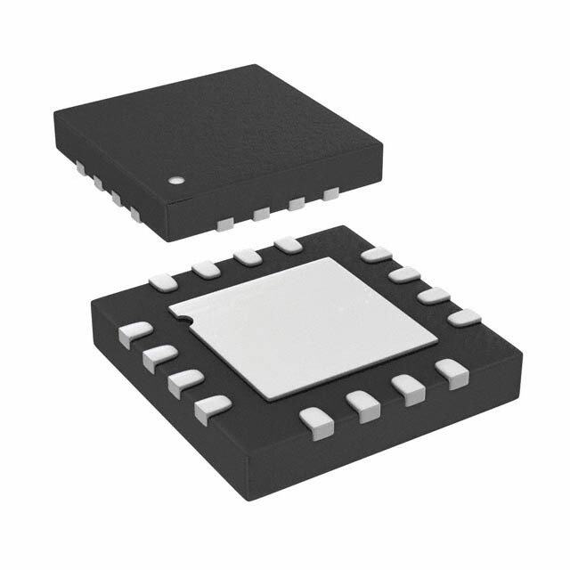
| 供应商器件封装 | 16-LFCSP-VQ (3x3) |
| 其它名称 | ADL5561ACPZ-R7CT |
| 包装 | 剪切带 (CT) |
| 压摆率 | 9800 V/µs |
| 增益带宽积 | - |
| 安装类型 | 表面贴装 |
| 封装/外壳 | 16-VFQFN 裸露焊盘,CSP |
| 工作温度 | -40°C ~ 85°C |
| 放大器类型 | RF/IF 差分 |
| 标准包装 | 1 |
| 电压-电源,单/双 (±) | 3 V ~ 3.6 V |
| 电压-输入失调 | - |
| 电流-电源 | 40mA |
| 电流-输入偏置 | 3µA |
| 电流-输出/通道 | - |
| 电路数 | 1 |
| 视频文件 | http://www.digikey.cn/classic/video.aspx?PlayerID=1364138032001&width=640&height=505&videoID=2245193153001 |
| 输出类型 | 差分 |


- 商务部:美国ITC正式对集成电路等产品启动337调查
- 曝三星4nm工艺存在良率问题 高通将骁龙8 Gen1或转产台积电
- 太阳诱电将投资9.5亿元在常州建新厂生产MLCC 预计2023年完工
- 英特尔发布欧洲新工厂建设计划 深化IDM 2.0 战略
- 台积电先进制程称霸业界 有大客户加持明年业绩稳了
- 达到5530亿美元!SIA预计今年全球半导体销售额将创下新高
- 英特尔拟将自动驾驶子公司Mobileye上市 估值或超500亿美元
- 三星加码芯片和SET,合并消费电子和移动部门,撤换高东真等 CEO
- 三星电子宣布重大人事变动 还合并消费电子和移动部门
- 海关总署:前11个月进口集成电路产品价值2.52万亿元 增长14.8%


PDF Datasheet 数据手册内容提取
2.9 GHz Ultralow Distortion RF/IF Differential Amplifier Data Sheet ADL5561 FEATURES FUNCTIONAL BLOCK DIAGRAM −3 dB bandwidth of 2.9 GHz (A = 6 dB) VCC V Low supply current: 40 mA RF Pin-strappable gain adjust: 6 dB, 12 dB, 15.5 dB ENBL Differential or single-ended input to differential output RG2 VON Low noise input stage: 2.1 nV/√Hz RTI at A = 12 dB VIP2 V Low broadband distortion (AV = 6 dB) RG1 VIP1 VCOM 10 MHz: −94 dBc HD2, −87 dBc HD3 RG1 70 MHz: −98 dBc HD2, −87 dBc HD3 VIN1 140 MHz: −95 dBc HD2, −87 dBc HD3 RG2 VIN2 VOP 250 MHz: −80 dBc HD2, −73 dBc HD3 IMD3s of −86 dBc at 250 MHz center GND RF SFaleswt s reattteli:n 9g.8 o Vf /2n ns s and overdrive recovery of 3 ns GND ADL5561 08004-001 Single-supply operation: 3 V to 3.6 V Figure 1. Power-down control Fabricated using the high speed XFCB3 SiGe process APPLICATIONS Differential ADC drivers Single-ended-to-differential conversion RF/IF gain blocks SAW filter interfacing GENERAL DESCRIPTION The ADL5561 is a high performance differential amplifier The device is optimized for wideband, low distortion performance. optimized for RF and IF applications. The amplifier offers low These attributes, together with its adjustable gain capability, noise of 2.1 nV/√Hz and excellent distortion performance over make this device the amplifier of choice for general-purpose IF a wide frequency range, making it an ideal driver for high speed and broadband applications where low distortion, noise, and power 8-bit to 16-bit analog-to-digital converters (ADCs). are critical. This device is optimized for the best combination of slew speed, bandwidth, and broadband distortion. These attributes The ADL5561 provides three gain levels of 6 dB, 12 dB, and 15.5 dB allow it to drive a wide variety of ADCs and make it ideally suited through a pin-strappable configuration. For the single-ended for driving mixers, pin diode attenuators, SAW filters, and multi- input configuration, the gains are reduced to 5.6 dB, 11.1 dB, and element discrete devices. 14.1 dB. Using an external series input resistor expands the amplifier gain flexibility and allows for any gain selection from Fabricated on the Analog Devices, Inc., high speed SiGe process, 0 dB to 15.5 dB. the ADL5561 is supplied in a compact 3 mm × 3 mm, 16-lead LFCSP package and operates over the temperature range of The quiescent current of the ADL5561 is typically 40 mA and, −40°C to +85°C. when disabled, consumes less than 3 mA, offering excellent input-to-output isolation. Rev. G Document Feedback Information furnished by Analog Devices is believed to be accurate and reliable. However, no responsibility is assumed by Analog Devices for its use, nor for any infringements of patents or other One Technology Way, P.O. Box 9106, Norwood, MA 02062-9106, U.S.A. rights of third parties that may result from its use. Specifications subject to change without notice. No license is granted by implication or otherwise under any patent or patent rights of Analog Devices. Tel: 781.329.4700 ©2009–2017 Analog Devices, Inc. All rights reserved. Trademarks and registered trademarks are the property of their respective owners. Technical Support www.analog.com
ADL5561 Data Sheet TABLE OF CONTENTS Features .............................................................................................. 1 Applications Information .............................................................. 14 Applications ....................................................................................... 1 Basic Connections ...................................................................... 14 Functional Block Diagram .............................................................. 1 Input and Output Interfacing ................................................... 15 General Description ......................................................................... 1 Gain Adjustment and Interfacing ............................................ 16 Revision History ............................................................................... 2 ADC Interfacing ......................................................................... 16 Specifications ..................................................................................... 3 Layout Considerations ............................................................... 18 Absolute Maximum Ratings ............................................................ 6 Soldering Information ............................................................... 19 ESD Caution .................................................................................. 6 Evaluation Board ........................................................................ 19 Pin Configuration and Function Descriptions ............................. 7 Outline Dimensions ....................................................................... 21 Typical Performance Characteristics ............................................. 8 Ordering Guide .......................................................................... 21 Circuit Description ......................................................................... 13 Basic Structure ............................................................................ 13 REVISION HISTORY 9/2017—Rev. F to Rev. G 3/2010—Rev A to Rev. B Changed CP-16-2 to CP-16-27 .................................... Throughout Changes to Figure 43 ...................................................................... 21 Updated Outline Dimensions ....................................................... 21 Changes to Ordering Guide .......................................................... 21 Changes to Ordering Guide .......................................................... 21 9/2009—Rev 0 to Rev. A 1/2014—Rev. E to Rev. F Changes to Features Section ............................................................ 1 Changes to ENBL Threshold Parameter, Table 1 ......................... 3 Changes to Table 1 ............................................................................. 3 Changes to Figure 5 ........................................................................... 8 9/2013—Rev. D to Rev. E Changes to Figure 9 and Figure 10 .................................................. 9 Added Input Resistance Tolerance of ±10% ................................. 3 Changes to Equation 1, Figure 32, and Figure 34 ...................... 15 Changes to Equation 2 ................................................................... 16 4/2013—Rev. C to Rev. D Changes to Figure 38, Figure 39, Figure 40, and Table 9........... 17 Changes to Table 1 ............................................................................ 3 Changes to Figure 43 ...................................................................... 19 Changes to Figure 6 and Figure 7 ................................................... 8 Moved Table 14 to ......................................................................... 19 6/2011—Rev. B to Rev. C 5/2009—Revision 0: Initial Version Changes to Figure 28 and Figure 29 ............................................. 12 Added Figure 30 and Figure 31; Renumbered Sequentially ..... 12 Changes to Ordering Guide .......................................................... 21 Rev. G | Page 2 of 24
Data Sheet ADL5561 SPECIFICATIONS VCC = 3.3 V, VCOM = 1.65 V, R = 200 Ω differential, A = 6 dB, C = 1 pF differential, f = 140 MHz, T = 25°C. L V L A Table 1. Parameter Conditions Min Typ Max Unit DYNAMIC PERFORMANCE −3 dB Bandwidth A = 6 dB, V ≤ 1.0 V p-p 2900 MHz V OUT A = 12 dB, V ≤ 1.0 V p-p 2300 MHz V OUT A = 15.5 dB, V ≤ 1.0 V p-p 1800 MHz V OUT Bandwidth for 0.1 dB Flatness A = 6 dB, V ≤ 1.0 V p-p 200 MHz V OUT A = 12 dB, V ≤ 1.0 V p-p 200 MHz V OUT A = 15.5 dB, V ≤ 1.0 V p-p 600 MHz V OUT Gain Accuracy A = 6 dB, R = open 0.15 dB V L A = 12 dB, R = open 0.05 dB V L A = 15.5 dB, R = open 0.05 dB V L Gain Supply Sensitivity VCC ± 10% −0.023 dB/V Gain Temperature Sensitivity −40°C to +85°C, A =15.5 dB 0.24 mdB/°C V Slew Rate Rise, A = 15.5 dB, R= 200 Ω, V = 2 V step 9.8 V/ns V L OUT Fall, A = 15.5 dB, R = 200 Ω, V = 2 V step 10.1 V/ns V L OUT Settling Time 2 V step to 1% 2 ns Overdrive Recovery Time V = 4 V to 0 V step, V ≤ ±10 mV 3 ns IN OUT Reverse Isolation (S12) 60 dB INPUT/OUTPUT CHARACTERISTICS Output Common Mode VCC/2 V Voltage Adjustment Range 1.4 to 1.8 V Maximum Output Voltage Swing 1 dB compressed 4.3 V p-p Output Common-Mode Offset Referenced to VCC/2 25 mV Output Common-Mode Drift −40°C to +85°C 170 µV/°C Output Differential Offset Voltage 1 mV CMRR 65 dB Output Differential Offset Drift −40°C to +85°C 15 µV/°C Input Bias Current 3 µA Input Resistance (Differential) A = 6 dB 400 Ω V A = 12 dB 200 Ω V A = 15.5 dB 133 Ω V Input Resistance (Single-Ended)1 A = 5.6 dB, R = 50 Ω 307 Ω V S A = 11.1 dB, R = 50 Ω 179 Ω V S A = 14.1 dB, R = 50 Ω 132 Ω V S Input Resistance Tolerance −10 +10 % Input Capacitance (Single-Ended) 0.3 pF Output Resistance (Differential) 12 Ω POWER INTERFACE Supply Voltage 3 3.3 3.6 V ENBL Threshold Device disabled, ENBL low 0.5 V Device enabled, ENBL high 1.5 V ENBL Input Bias Current ENBL high −27 µA ENBL low −300 µA Quiescent Current ENBL high 37 40 44.5 mA ENBL low 3 mA Rev. G | Page 3 of 24
ADL5561 Data Sheet Parameter Conditions Min Typ Max Unit 10 MHz NOISE/HARMONIC PERFORMANCE Second/Third Harmonic Distortion A = 6 dB, R = 200 Ω, V = 2 V p-p −94/−87 dBc V L OUT A = 12 dB, R = 200 Ω, V = 2 V p-p −92/−88 dBc V L OUT A = 15.5 dB, R = 200 Ω, V = 2 V p-p −95/−87 dBc V L OUT Output Third-Order Intercept/Third-Order A = 6 dB, R = 200 Ω, V = 2 V p-p +42.7/−89 dBm/dBc V L OUT Intermodulation Distortion composite (2 MHz spacing) A = 12 dB, R = 200 Ω, V = 2 V p-p +41/−85 dBm/dBc V L OUT composite (2 MHz spacing) A = 15.5 dB, R = 200 Ω, V = 2 V p-p +40/−85 dBm/dBc V L OUT composite (2 MHz spacing) Noise Spectral Density (RTI) A = 6 dB 3 nV/√Hz V A = 12 dB 2.1 nV/√Hz V A = 15.5 dB 1.7 nV/√Hz V 1 dB Compression Point (RTO) A = 6 dB 12.5 dBm V A = 12 dB 12.5 dBm V A = 15.5 dB 12.5 dBm V 70 MHz NOISE/HARMONIC PERFORMANCE Second/Third Harmonic Distortion A = 6 dB, R = 200 Ω, V = 2 V p-p −98/−87 dBc V L OUT A = 12 dB, R = 200 Ω, V = 2 V p-p −93/−83 dBc V L OUT A = 15.5 dB, R = 200 Ω, V = 2 V p-p −93/−82 dBc V L OUT Output Third-Order Intercept/Third-Order A = 6 dB, R = 200 Ω, V = 2 V p-p +45/−93 dBm/dBc V L OUT Intermodulation Distortion composite (2 MHz spacing) A = 12 dB, R = 200 Ω, V = 2 V p-p +43/−89 dBm/dBc V L OUT composite (2 MHz spacing) A = 15.5 dB, R = 200 Ω, V = 2 V p-p +41/−86 dBm/dBc V L OUT composite (2 MHz spacing) Noise Spectral Density (RTI) A = 6 dB 3 nV/√Hz V A = 12 dB 2.1 nV/√Hz V A = 15.5 dB 1.7 nV/√Hz V 1 dB Compression Point (RTO) A = 6 dB 12.3 dBm V A = 12 dB 12.3 dBm V A = 15.5 dB 12.3 dBm V 140 MHz NOISE/HARMONIC PERFORMANCE Second/Third Harmonic Distortion A = 6 dB, R = 200 Ω, V = 2 V p-p −95/−87 dBc V L OUT A = 12 dB, R = 200 Ω, V = 2 V p-p −83/−83 dBc V L OUT A = 15.5 dB, R = 200 Ω, V = 2 V p-p −83/−82 dBc V L OUT Output Third-Order Intercept/Third-Order A = 6 dB, R = 200 Ω, V = 2 V p-p +49/−102 dBm/dBc V L OUT Intermodulation Distortion composite (2 MHz spacing) A = 12 dB, R = 200 Ω, V = 2 V p-p +48/−100 dBm/dBc V L OUT composite (2 MHz spacing) A = 15.5 dB, R = 200 Ω, V = 2 V p-p +39/−96 dBm/dBc V L OUT composite (2 MHz spacing) Noise Spectral Density (RTI) A = 6 dB 3 nV/√Hz V A = 12 dB 2.1 nV/√Hz V A = 15.5 dB 1.7 nV/√Hz V 1 dB Compression Point (RTO) A = 6 dB 12 dBm V A = 12 dB 12 dBm V A = 15.5 dB 12 dBm V Rev. G | Page 4 of 24
Data Sheet ADL5561 Parameter Conditions Min Typ Max Unit 250 MHz NOISE/HARMONIC PERFORMANCE Second/Third Harmonic Distortion A = 6 dB, R = 200 Ω, V = 2 V p-p −80/−73 dBc V L OUT A = 12 dB, R = 200 Ω, V = 2 V p-p −76/−70 dBc V L OUT A = 15.5 dB, R = 200 Ω, V = 2 V p-p −78/−72 dBc V L OUT Output Third-Order Intercept/Third-Order A = 6 dB, R = 200 Ω, V = 2 V p-p +41/−86 dBm/dBc V L OUT Intermodulation Distortion composite (2 MHz spacing) A = 12 dB, R = 200 Ω, V = 2 V p-p +40/−84 dBm/dBc V L OUT composite (2 MHz spacing) A = 15.5 dB, R = 200 Ω, V = 2 V p-p +39/−83 dBm/dBc V L OUT composite (2 MHz spacing) Noise Spectral Density (RTI) A = 6 dB 3.2 nV/√Hz V A = 12 dB 2.2 nV/√Hz V A = 15.5 dB 1.7 nV/√Hz V 1 dB Compression Point (RTO) A = 6 dB 12 dBm V A = 12 dB 12 dBm V A = 15.5 dB 12 dBm V 500 MHz NOISE/HARMONIC PERFORMANCE Second/Third Harmonic Distortion A = 6 dB, R = 200 Ω, V = 1 V p-p −69/−57 dBc V L OUT A = 12 dB, R = 200 Ω, V = 1 V p-p −72/−60 dBc V L OUT A = 15.5 dB, R = 200 Ω, V = 1V p-p −66/−61 dBc V L OUT Output Third-Order Intercept/Third-Order A = 6 dB, R = 200 Ω, V = 1 V p-p +40/−97 dBm/dBc V L OUT Intermodulation Distortion composite (2 MHz spacing) A = 12 dB, R = 200 Ω, V = 1 V p-p +36/−90 dBm/dBc V L OUT composite( 2 MHz spacing) A = 15.5 dB, R = 200 Ω, V = 1 V p-p +34/−75 dBm/dBc V L OUT composite (2 MHz spacing) Noise Spectral Density (RTI) A = 6 dB 4.1 nV/√Hz V A = 12 dB 2.4 nV/√Hz V A = 15.5 dB 1.8 nV/√Hz V 1000 MHz NOISE/HARMONIC PERFORMANCE Second/Third Harmonic Distortion A = 6 dB, R = 200 Ω, V = 1 V p-p −58/−53 dBc V L OUT A = 12 dB, R = 200 Ω, V = 1 V p-p −55/−50 dBc V L OUT A = 15.5 dB, R = 200 Ω, V = 1 V p-p −57/−50 dBc V L OUT Output Third-Order Intercept/Third-Order A = 6 dB, R = 200 Ω, V = 1 V p-p +18/−54 dBm/dBc V L OUT Intermodulation Distortion composite (2 MHz spacing) A = 12 dB, R = 200 Ω, V = 1 V p-p +18/−56 dBm/dBc V L OUT composite (2 MHz spacing) A = 15.5 dB, R = 200 Ω, V = 1 V p-p +18/−46 dBm/dBc V L OUT composite (2 MHz spacing) Noise Spectral Density (RTI) A = 6 dB 6 nV/√Hz V A = 12 dB 2.6 nV/√Hz V A = 15.5 dB 1.8 nV/√Hz V 1 See the Applications Information section for a discussion of single-ended input, dc-coupled operation. Rev. G | Page 5 of 24
ADL5561 Data Sheet ABSOLUTE MAXIMUM RATINGS Stresses at or above those listed under Absolute Maximum Table 2. Ratings may cause permanent damage to the product. This is a Parameter Rating stress rating only; functional operation of the product at these Supply Voltage (VCC) 3.6 V or any other conditions above those indicated in the operational VIP1, VIP2, VIN1, VIN2 VCC + 0.5 V section of this specification is not implied. Operation beyond Internal Power Dissipation 155 mW the maximum operating conditions for extended periods may θ 98.3°C/W JA affect product reliability. Maximum Junction Temperature 125°C ESD CAUTION Operating Temperature Range −40°C to +85°C Storage Temperature Range −65°C to +150°C Rev. G | Page 6 of 24
Data Sheet ADL5561 PIN CONFIGURATION AND FUNCTION DESCRIPTIONS D D D D N N N N G G G G 6 5 4 3 1 1 1 1 VIP2 1 12 ENBL VIP1 2 ADL5561 11 VOP VIN1 3 TOP VIEW 10 VON (Not to Scale) VIN2 4 9 VCOM 5 6 7 8 C C C C C C C C V V V V NOTES 1 . EIGMXRPPOEOUDSNAEDND CP PELA ATDNHDEEL.REM. CAOL NANNEDC ETL TEOC TAR LICOAWL 08004-031 Figure 2. Pin Configuration Table 3. Pin Function Descriptions Pin No. Mnemonic Description 1 VIP2 Balanced Differential Input. Biased to VCOM, typically ac-coupled. Input for A = 12 dB gain, strapped to V VIP1 for A = 15.5 dB. v 2 VIP1 Balanced Differential Input. Biased to VCOM, typically ac-coupled. Input for A = 6 dB gain, strapped to V VIP2 for A = 15.5 dB. v 3 VIN1 Balanced Differential Input. Biased to VCOM, typically ac-coupled. Input for A = 6 dB gain, strapped to V VIN2 for A = 15.5 dB. v 4 VIN2 Balanced Differential Input. Biased to VCOM, typically ac-coupled. Input for A = 12 dB gain, strapped to V VIN1 for A = 15.5 dB. v 5, 6, 7, 8 VCC Positive Supply. 9 VCOM Common-Mode Voltage. A voltage applied to this pin sets the common-mode voltage of the input and output. Typically decoupled to ground with a 0.1 µF capacitor. With no reference applied, input and output common mode floats to midsupply (VCC/2). 10 VON Balanced Differential Output. Biased to VCOM, typically ac-coupled. 11 VOP Balanced Differential Output. Biased to VCOM, typically ac-coupled. 12 ENBL Enable. Apply positive voltage (1.0 V < ENBL < VCC) to activate device. 13, 14, 15, 16 GND Ground. Connect to low impedance ground. EP Exposed Paddle. Connect to a low impedance thermal and electrical ground plane. Rev. G | Page 7 of 24
ADL5561 Data Sheet TYPICAL PERFORMANCE CHARACTERISTICS VCC = 3.3 V, VCOM = 1.65 V, R = 200 Ω differential, A = 6 dB, C = 1 pF differential, f = 140 MHz, and T = 25°C. L V L A 16 14 MAXIMUM GAIN –40°C +25°C +85°C 12 14 10 12 MID GAIN m) B) B 8 d d N ( 10 B ( GAI P1d 6 O MAX GAIN –40°C 8 MAX GAIN +25°C 4 MAX GAIN +85°C MID GAIN –40°C MID GAIN +25°C 6 MINIMUM GAIN 2 MMIIDN GGAAIINN +–4805°°CC MIN GAIN +25°C MIN GAIN +85°C 410M 100MFREQUENCY (Hz)1G 10G 08004-002 00 50 FR10E0QUENCY (1M5H0z) 200 250 08004-016 Figure 3. Gain vs. Frequency Response for 200 Ω Differential Load, Figure 6. Output P1dB (OP1dB) vs. Frequency at AV = 6 dB, AV = 12 dB, and AV = 6 dB, AV = 12 dB, and AV = 15.5 dB over Temperature AV = 15.5 dB over Temperature, 200 Ω Differential Load 16 14 –40°C MAX GAIN –40°C MAXIMUM GAIN +25°C MAX GAIN +25°C +85°C 12 MAX GAIN +85°C 14 MID GAIN –40°C MID GAIN +25°C MID GAIN +85°C 10 MIN GAIN –40°C 12 MIN GAIN +25°C B) MID GAIN Bm) 8 MIN GAIN +85°C d d N ( 10 B ( GAI P1d 6 O 8 4 6 MINIMUM GAIN 2 410M 100MFREQUENCY (Hz)1G 10G 08004-003 00 50 FR10E0QUENCY (1M5H0z) 200 250 08004-017 Figure 4. Gain vs. Frequency Response for 1 kΩ Differential Load Figure 7. Output P1dB (OP1dB) vs. Frequency at AV = 6 dB, AV = 12 dB, and AV = 6 dB, AV = 12 dB, and AV = 15.5 dB over Temperature AV = 15.5 dB over Temperature, 1 kΩ Differential Load 16 8 14 AAAVVV MMMAIIDNXIMIMUUMM Hz) 7 AAAVVV MMMAIIDNXIMIMUUMM √ 12 V/ 6 n B) Y ( FIGURE (d 108 AL DENSIT 45 E R NOIS 6 PECT 3 S 4 E 2 S OI 2 N 1 010 FREQUE1N0C0Y (MHz) 1000 08004-004 010 FREQUE1N0C0Y (MHz) 1000 08004-015 Figure 5. Noise Figure vs. Frequency at Figure 8. Noise Spectral Density vs. Frequency at AV = 6 dB, AV = 12 dB, and AV = 15.5 dB AV = 6 dB, AV = 12 dB, and AV = 15.5 dB Rev. G | Page 8 of 24
Data Sheet ADL5561 60 –40 0 AV MAXIMUM AV MAXIMUM AV MID AV MID 50 AV MINIMUM –60 AV MINIMUM –20 OIP3 (dBm) 234000 IMD3, R = 200Ω (dBc)L––11–208000 –––864000IMD3, R= 1kΩ (dBc)L 10 –140 –100 0 –160 –120 0 50 FR1E00QUENCY (1M5H0z) 200 250 08004-018 0 50 FR1E00QUENCY (1M5H0z) 200 250 08004-020 Figure 9. Output Third-Order Intercept at Three Gains, Output Level at 2 V p-p Figure 12. Two-Tone Output IMD vs. Frequency, Composite, RL = 200 Ω Output Level at 2 V p-p Composite, RL = 200 Ω and RL = 1 kΩ 60 50 +85°C MAX GAIN +25°C MAX GAIN 45 –40°C MAX GAIN 50 40 35 40 m) m) 30 B B 3 (d 30 3 (d 25 P P OI OI 20 20 15 10 10 5 0 0 0 50 FR1E00QUENCY (1M5H0z) 200 250 08004-019 –2 –1 0 POUT1/TONE (d2Bm) 3 4 5 08004-021 Figure 10. Output Third-Order Intercept vs. Frequency, Over Temperature, Figure 13. Output Third-Order Intercept (OIP3) vs. Power (POUT), Output Level at 2 V p-p Composite, RL = 200 Ω Frequency 140 MHz, AV = 15.5 dB 60 –70 AV MAXIMUM AV MAXIMUM 55 AAVV MMIIDNIMUM –75 AAVV MMIIDNIMUM –80 50 –85 Bm) Bc) OIP3 (d 45 IMD (d ––9950 40 –100 35 –105 30 –110 0 50 FR1E00QUENCY (1M5H0z) 200 250 08004-005 0 50 FR1E00QUENCY (1M5H0z) 200 250 08004-006 Figure 11. OIP3 vs. Frequency (Single-Ended Input) Figure 14. IMD vs. Frequency (Single-Ended Input) Rev. G | Page 9 of 24
ADL5561 Data Sheet –40 0 –40 0 MONIC DISTORTION HD2 (dBc) ––11––20860000 AAAVVV MMMAIIDNXIMIMUUMM ––––86420000 MONIC DISTORTION HD3 (dBc) MONIC DISTORTION HD2 (dBc)––11––20860000 AAAVVV MMMAIIDNXIMIMUUMM ––––86420000 MONIC DISTORTION HD3 (dBc) HAR –140 –100HAR HAR–140 –100HAR –1600 50 FR1E00QUENCY (1M5H0z) 200 250–120 08004-022 –1600 50 FR1E00QUENCY (1M5H0z) 200 250–120 08004-026 Figure 15. Harmonic Distortion (HD2/HD3) vs. Frequency at AV = 6 dB, Figure 18. Harmonic Distortion (HD2/HD3) vs. Frequency at AV = 6 dB, AV = 12 dB, and AV = 15.5 dB, Output Level at 2 V p-p, RL = 200 Ω AV = 12 dB, and AV = 15.5 dB, Output Level at 2 V p-p, RL = 1 k Ω –40 0 –20 +85°C +25°C –40°C –30 c) –60 –20 c) 2 (dB 3 (dB dBc) –40 HD –80 –40 HD N ( ON ON TIO –50 STORTI–100 –60 STORTI DISTOR –60 HARMONIC DI––114200 ––18000HARMONIC DI HARMONIC ––8700 HHDD23 –90 –1600 50 FR1E00QUENCY (1M5H0z) 200 250–120 08004-024 –100–2 –1 0 P1OUT (dBm2) 3 4 5 08004-023 Figure 16. Harmonic Distortion (HD2/HD3) vs. Frequency, Figure 19. Harmonic Distortion (HD2/HD3) vs. Power, Frequency 140 MHz, Three Temperatures, Output Level at 2 V p-p, RL = 200 Ω AV = 15.5 dB –40 0 –60 0 Bc) –60 ++–482055°°°CCC –20 Bc) Bc) ––7605 AAAVVV MMMAIIDNXIMIMUUMM ––2100 Bc) D2 (d D3 (d D2 (d –75 –30 D3 (d H –80 –40 H H H N N N N O O O –80 –40 O ORTI–100 –60 ORTI ORTI –85 –50 ORTI ST ST ST ST DI DI DI –90 –60 DI ONIC –120 –80 ONIC ONIC –95 –70 ONIC M M M M HAR–140 –100HAR HAR–100 –80 HAR –105 –90 –1600 50 FR1E00QUENCY (1M5H0z) 200 250–120 08004-025 –1100 50 FR1E00QUENCY (1M5H0z) 200 250–100 08004-007 Figure 17. Harmonic Distortion (HD2/HD3) vs. Frequency, Over Temperature, Figure 20. Harmonic Distortion (HD2/HD3) vs. Frequency (Single-Ended Input) Output Level at 2 V p-p, RL = 1 kΩ Rev. G | Page 10 of 24
Data Sheet ADL5561 –30 –50 –50 –60 D2 (dBc) ––5400 AAAVVV MMMAIIDNXIMIMUUMM ––7600 D3 (dBc) D2 (dBc) ––6505 AAAVVV MMMAIIDNXIMIMUUMM ––7605 D3 (dBc) H H H –65 –75 H N N N N RTIO –60 –80 RTIO RTIO –70 –80 RTIO O O O O ST –70 –90 ST ST –75 –85 ST DI DI DI DI ONIC –80 –100 ONIC ONIC –80 –90 ONIC M M M M R R R –85 –95 R A A A A H –90 –110 H H H –90 –100 –1000 100 200 300 400RLO5A0D0 (Ω)600 700 800 900 1k–120 08004-008 –951.1 1.2 1.3 1.4 VCO1M.5 (V) 1.6 1.7 1.8 1.9–105 08004-009 Figure 21. Harmonic Distortion (HD2/HD3) vs. RLOAD Figure 24. Harmonic Distortion (HD2/HD3) vs. VCOM 1.0 0 AV MAXIMUM 0.9 AV MID –20 AV MINIMUM 0.8 –40 AGE (V) ENABLE ELAY (ns) 00..67 ––8600 Degrees) VOLT 2V p-p OUTPUT GROUP D 00..45 ––112000PHASE ( 0.3 –140 0.2 –160 TIME (2.5ns/DIV) 08004-045 0.10 100 200 300 FR4E00QUE5N0C0Y (6M0H0z) 700 800 900 1k–180 08004-010 Figure 22. ENBL Time Domain Response Figure 25. Group Delay and Phase vs. Frequency 110 80 AV MAXIMUM AV MID 2V p-p OUTPUT 100 AV MINIMUM 70 90 RL = 1kΩ 60 V) 80 50 E ( B) B) G d d LTA RR ( 70 RL = 200Ω 40 RR ( O M M V C 60 30 C 50 20 40 10 TIME (2.5ns/DIV) 08004-046 3010M FREQU1E00NMCY (Hz) 1G0 08004-011 Figure 23. Large Signal Pulse Response, AV = 15.5 dB Figure 26. Common-Mode Rejection Ratio (CMRR) vs. Frequency Rev. G | Page 11 of 24
ADL5561 Data Sheet 0 800 8 AV MAXIMUM AV MID –10 700 AV MINIMUM 7 600 6 –20 Ω) pF) S12 (dB) ––4300 DISABLED SISTANCE ( 540000 54 ACITANCE ( ENABLED RE 300 3 AP C –50 200 2 –60 100 1 –700 0.5 1.0FREQUE1N.5CY (GHz)2.0 2.5 3.0 08004-012 010M FREQU10E0NMCY (Hz) 1G0 08004-051 Figure 27. Reverse Isolation (S12) vs. Frequency Figure 30. Input Resistance and Capacitance vs. Frequency 1000 20 16 10 900 AAAVVV MMMIAIDNXIMIMUUMM 10 14 AAAVVV MMMAIIDNXIMIMUUMM Ω) 800 0 8 DANCE MAGNITUDE ( 765400000000 ––––12340000 PHASE (Degrees) RESISTANCE (Ω)112086 64 NDUCTANCE (nH) E 300 –50 I P M 4 I 200 –60 2 100 –70 2 010M FREQU10E0NMCY (Hz) 1G–80 08004-013 010M FR1E0Q0MUENCY (Hz) 1G 2G0 08004-052 Figure 28. Input Impedance Magnitude and Phase vs. Frequency Figure 31. Output Resistance and Inductance vs. Frequency 16 40 AV MAXIMUM AV MID 14 AV MINIMUM 35 E (Ω) 12 30 D TU 10 25 es) DANCE MAGNI 86 2105 PHASE (Degre E MP 4 10 I 2 5 010M FREQU10E0NMCY (Hz) 1G0 08004-050 Figure 29. Output Impedance Magnitude and Phase vs. Frequency Rev. G | Page 12 of 24
Data Sheet ADL5561 CIRCUIT DESCRIPTION BASIC STRUCTURE The amplifier is designed to provide high differential open-loop gain and an output common-mode circuit that enables the user The ADL5561 is a low noise, low power, fully differential amplifier/ to change the common-mode voltage from a VCOM pin. The ADC driver that uses a 3.3 V supply. It provides three gain options amplifier is designed to provide superior low distortion at (6 dB, 12 dB, and 15.5 dB) without the need for external resistors frequencies up to and beyond 300 MHz with low noise and and has wide bandwidths of 2.6 GHz for 6 dB, 2.3 GHz for 12 low power consumption. The low distortion and noise are dB, and 2.1 GHz for 15.5 dB. Differential input impedance is realized with a 3.3 V power supply at 40 mA. 400 Ω for 6 dB, 200 Ω for 12 dB, and 133 Ω for 15.5 dB. It has a differential output impedance of 10 Ω and an output common- The ADL5561 is very flexible in terms of I/O coupling. It can be mode adjust voltage of 1.25 V to 1.85 V. ac-coupled or dc-coupled at the inputs and/or the outputs within the specified input and output common-mode levels. The input 0.1µF 400Ω of the device can be configured as single-ended or differential with + similar distortion performance. Due to the internal connections 1/2 RS VIP2 100Ω 5Ω between the inputs and outputs, keep the output common-mode VIP1 200Ω AC VIN1 200Ω RL voltage between 1.25 V and 1.85 V for the best distortion. For a dc-coupled input, the input common mode should be 1/2 RS VIN2 100Ω 5Ω between 1 V and 2.3 V for the best distortion. The device has 0.1+µF 400Ω 08004-032 bace-ecno cuhpaleradc, ttehriez eindp uusti nang d2 oVu tpp-upt icnotom 2m0o0n Ω-m. Iof dthee v ionlptaugtess a arree Figure 32. Basic Structure set by VCC/2 when no external circuitry is used. The ADL5561 The ADL5561 is composed of a fully differential amplifier with provides an output common-mode voltage set by VCOM, which on-chip feedback and feed-forward resistors. The two feed- allows driving an ADC directly without external components, forward resistors on each input set this pin-strappable amplifier such as a transformer or ac-coupling capacitors, provided that in three different gain configurations of 6 dB, 12 dB, and 15.5 dB. the VCOM of the amplifier is within the VCOM of the ADC. For dc-coupled requirements, the input VCM must be set by the VCOM pin in all three gain settings. Rev. G | Page 13 of 24
ADL5561 Data Sheet APPLICATIONS INFORMATION BASIC CONNECTIONS Pin 1 to Pin 4, Pin 10, and Pin 11 are biased at 1/2 VCC above ground and can be dc-coupled (if within the specified input and Figure 33 shows the basic connections for operating the ADL5561. output common-mode voltages levels) or ac-coupled, as shown VCC should be 3.3 V with each supply pin decoupled with at least in Figure 33. one low inductance surface-mount ceramic capacitor of 0.1 μF To enable the ADL5561, the ENBL pin must be pulled high. placed as close as possible to the device. The VCOM pin (Pin 9) Pulling the ENBL pin low puts the ADL5561 in sleep mode, should also be decoupled using a 0.1 μF capacitor. reducing the current consumption to 3 mA at ambient. The gain of the part is determined by the pin-strappable input configuration. When Input A is applied to VIP1 and Input B is applied to VIN1, the gain is 6 dB (minimum gain; see Equation 1 and Equation 2). When Input A is applied to VIP2 and Input B is applied to VIN2, the gain is 12 dB (middle gain). When Input A is applied to VIP1 and VIP2 and Input B is applied to VIN1 and VIN2, the gain is 15.5 dB (maximum gain). VCC 16 15 14 13 GND GND GND GND A 1 VIP2 ENBL12 RS/2 0.1µF 2 VIP1 VOP11 BASLOANUCRECDE AC ADL5561 RL BLOALAADNCED 0.1µF B 3 VIN1 VON10 RS/2 4 VIN2 VCOM 9 0.1µF VCC VCC VCC VCC 5 6 7 8 VCC 10µF 0.1µF 08004-033 Figure 33. Basic Connections Rev. G | Page 14 of 24
Data Sheet ADL5561 INPUT AND OUTPUT INTERFACING Single-Ended Input to Differential Output The ADL5561 can be configured as a differential input to differential output driver, as shown in Figure 34. The differential The ADL5561 can also be configured in a single-ended input broadband input is provided by the ETC1-1-13 balun transformer, to differential output driver, as shown in Figure 36. In this and the two 34.8 Ω resistors provide a 50 Ω input match for configuration, the gain of the part is reduced due to the the three input impedances that change with the variable gain application of the signal to only one side of the amplifier. The strapping. The input and output 0.1 μF capacitors isolate the strappable gain values are listed in Table 6 with the required VCC/2 bias from the source and balanced load. The load must terminations to match to a 50 Ω source using R1 and R2. Note be 200 Ω to provide the expected ac performance (see the that R1 must equal the parallel value of the source and R2. The Specifications section and the Typical Performance input and output 0.1 μF capacitors isolate the VCC/2 bias from Characteristics section). the source and the balanced load. The performance for this configuration is shown in Figure 11, Figure 14, and Figure 20. 3.3V 3.3V 0.1µF ETC1-1-13 0.1+µF A VVIIPP21 + RL 0.1µF VIP2 0.1µF A50CΩ RR12 0.1µ+FB VVIINN12 0.1+µF R22L 50Ω R2 + AB VVVIIINNP112 0.1+µF RR22LL AC + + 0.1µF R1 NOTES 1. FOR 6dB GAIN (AV = 2), CONNECT INPUT A TO VIP1 AND INPUT B TO VIN1. 23 .. FFAOONRRD 11IN25Pd.5UBdT BG BAG ITANOI N( A B(VAO V=T H=4 ) 6,V )CI,N OC1NO ANNNENDCE TVC ITINN I2PN.UPTU TA AT OT OV IBPO2 TAHN DV IIPN1P AUNTD B V TIOP2 VIN2. 08004-036 N1.O FTOERS 5.6dB GAIN (AV = 1.9), CONNECT INPUT A TO VIP1 Figure 34. Differential-Input-to-Differential-Output Configuration AND INPUT B TO VIN1. 2. FOR 11.1dB GAIN (AV = 3.6), CONNECT INPUT A TO VIP2 TGaabinle ( d4B. D) ifferential TermRi1n a(Ωti)o n Values for RF2ig (uΩr)e 34 3 . FAVOINPRD1 1IAN4NP.1DUd TVB I BPG 2TA OAINN V (DAIN VIN2 =.P U5.T1 )B, C TOON BNOETCHT VININP1U TA NAD T VOI NB2O.TH 08004-037 Figure 36. Single-Ended Input to Differential-Output Configuration 6 28.7 28.7 12 33.2 33.2 Table 6. Single-Ended Termination Values for Figure 36 15.5 40.2 40.2 Gain (dB) R1 (Ω) R2 (Ω) 5.6 27 60 The differential gain of the ADL5561 is dependent on the 11.1 29 69 source impedance and load, as shown in Figure 35. 14.1 30 77 0.1µF 400Ω + 1/2 RS VIP2 100Ω 5Ω 0.1µF The single-ended gain configuration of the ADL5561 is VIP1 200Ω + RL dependent on the source impedance and load, as shown in 2 Figure 37. AC VIN1 200Ω VIN2 100Ω 5Ω 0.1µF R2L 400Ω 1/2 RS + 0.1µF 400Ω 0.1µF VIP2 100Ω 5Ω 0.1µF + Figure 35. Differential Input Loading Circuit 08004-027 RS R2 + VVIINP11 220000ΩΩ + R2L VIN2 100Ω 5Ω 0.1µF R2L The differential gain can be determined using the following AC + + formula. The values of R for each gain configuration are 0.1µF 400Ω IN shown in Table 5. R1 08004-038 400 R Figure 37. Single-Ended Input Loading Circuit A L (1) V R 10R IN L Table 5. Values of R for Differential Gain IN Gain (dB) RIN (Ω) 6 200 12 100 15.5 66.7 Rev. G | Page 15 of 24
ADL5561 Data Sheet The single-ended gain can be determined using the following The necessary shunt component, R , to match to the source SHUNT formula. The values of R and R for each gain configuration impedance, R, can be expressed as IN X S are shown in Table 7. 1 R = (4) 400 R2 R +R R SHUNT 1 1 A = × × X S× L (2) − V1 R ×R2 R +R2 R 10+R R R +R RIN+RSS+R2 S X L The insertion loss Sand thSEeR rIEeSsultanINt power gain for multiple shunt resistor values are summarized in Table 8. The source resistance Table 7. Values of R and R for Single-Ended Gain IN X and input impedance need careful attention when using Equation 3 Gain (dB) R (Ω) R (Ω) IN X and Equation 4. The reactance of the input impedance of the 5.6 200 R2 || 3071 ADL5561 and the ac-coupling capacitors must be considered 11.1 100 R2 || 1791 before assuming they make a negligible contribution. 14.1 66.7 R2 || 1321 1 These values are based on a 50 Ω output match. Table 8. Gain Adjustment Using Series Resistors GAIN ADJUSTMENT AND INTERFACING Il (dB) RIN (Ω) RS (Ω) RSERIES (Ω) RSHUNT (Ω) 2 400 50 105 54.9 The effective gain of the ADL5561 can be reduced using a number 4 400 50 232 54.9 of techniques. A matched attenuator network can reduce the 2 200 50 51.1 61.9 effective gain, but this requires the addition of a separate 4 200 50 115 59 component that can be prohibitive in size and cost. Instead, a 2 133 50 34.8 71.5 simple voltage divider can be implemented using the combination 2 400 200 102 332 of an addition series resistor at the amplifier input and the input 4 400 200 232 294 impedance of the ADL5561, as shown in Figure 38. A shunt 2 200 200 51.1 976 resistor is used to match to the impedance of the previous stage. 4 200 200 115 549 VIN1 2 400 50 105 54.9 1/2 RS 0.1µF 1/2RSERIES VIN2 4 400 50 232 54.9 1/2 RSHUNT 2 200 50 51.1 61.9 1/A2 CRS 0.1µF 1/2RSERIES VVIIPP12 ADL5561 1/2 RSHUNT 08004-039 AThDeC A DINLT55E6R1F iAs aC hIiNghG o utput linearity amplifier that is optimized Figure 38. Gain Adjustment Using Series Resistor for ADC interfacing. There are several options available to the Figure 38 shows a typical implementation of the divider concept designer when using the ADL5561. Figure 39 shows a simplified that effectively reduces the gain by adding attenuation at the wideband interface with the ADL5561 driving the AD9445. The input. For frequencies less than 100 MHz, the input impedance AD9445 is a 14-bit, 125 MSPS ADC with a buffered wideband input. of the ADL5561 can be modeled as a real 133 Ω, 200 Ω, or 400 Ω For optimum performance, the ADL5561 should be driven dif- resistance (differential) for maximum, middle, and minimum ferentially using an input balun. Figure 39 uses a wideband 1:1 gains, respectively. Assuming that the frequency is low enough transmission line balun followed by two 34.8 Ω resistors in parallel to ignore the shunt reactance of the input and high enough so with the three input impedances (which change with the gain that the reactance of moderately sized ac-coupling capacitors selection of the ADL5561) to provide a 50 Ω differential input can be considered negligible, the insertion loss, Il, due to the impedance. This provides a wideband match to a 50 Ω source. shunt divider can be expressed as The ADL5561 is ac-coupled from the AD9445 to avoid common- R mode dc loading. The 33 Ω series resistors help to improve the Il(dB)=20log IN (3) R +R isolation between the ADL5561 and any switching currents present SERIES IN at the analog-to-digital sample-and-hold input circuitry. The AD9445 input presents a 2 kΩ differential load impedance and requires a 2 V p-p differential input swing to reach full scale (VREF = 1 V). 3.3V ETC1-1-13 0.1µF A VIP2 VOP 0.1µF 33Ω 50Ω 34.8Ω + VIP1 + AVDIN94+45 14 AC 0.1µF B VIN1 ADL5561 0.1µF 33Ω 14-BIT ADC VIN– 34.8Ω + VIN2 VON + 08004-040 Figure 39. Wideband ADC Interfacing Example Featuring the AD9445 Rev. G | Page 16 of 24
Data Sheet ADL5561 This circuit provides variable gain, isolation, and source matching The wideband frequency response is an advantage in broad- for the AD9445. Using this circuit with the ADL5561 in a gain band applications, such as predistortion receiver designs and of 6 dB, an SFDR performance of 87 dBc is achieved at 140 MHz instrumentation applications. However, by designing for a wide and a −3 dB bandwidth of 760 MHz, as shown in Figure 40 analog input frequency range, the cascaded SNR performance and Figure 41. is somewhat degraded due to high frequency noise aliasing into 0 the wanted Nyquist zone. –10 ADL5561 DRIVING THE AD9445 14-BIT ADC GAIN = 6dB An alternative narrow-band approach is presented in Figure 42. –20 INPUT = 140MHz –30 SNR = 64.69dBc By designing a narrow band-pass antialiasing filter between the SFDR = 87.44dBc –40 NOISE FLOOR = –107.9dB ADL5561 and the target ADC, the output noise of the ADL5561 FUND = –1.096dBFS –50 SECOND = –89.64dBc outside of the intended Nyquist zone can be attenuated, helping –60 THIRD = –87.52dBc to preserve the available SNR of the ADC. In general, the SNR S) –70 dBF –80 improves several decibels when including a reasonable order anti- ( –90 aliasing filter. In this example, a low loss 1:1 input transformer is –100 used to match the ADL5561 balanced input to a 50 Ω unbalanced –110 source, resulting in minimum insertion loss at the input. –120 –130 Figure 42 is optimized for driving some of the Analog Devices –140 popular unbuffered ADCs, such as the AD9246, AD9640, –150 0 6.25 12.50 18.75F2R5E.0Q0U3E1N.2C5Y 3(M7.H50z)43.75 50.00 56.25 62.50 08004-044 arencdo mADm6en65d5at. iToanbs lfeo 9r pinocpluudlaers I aFn staiamlipasliinngg cfielntetre rc ofrmeqpuoennecnite s. Figure 40. Measured Single-Tone Performance of the Inductor L5 works in parallel with the on-chip ADC input Circuit in Figure 39 for a 140 MHz Input Signal capacitance and a portion of the capacitance presented by C4 to 0 form a resonant tank circuit. The resonant tank helps to ensure –1 that the ADC input looks like a real resistance at the target center –2 frequency. The L5 inductor shorts the ADC inputs at dc, which introduces a zero into the transfer function. In addition, the ac –3 coupling capacitors introduce additional zeros into the transfer –4 S) function. The final overall frequency response takes on a band- BF –5 pass characteristic, helping to reject noise outside of the intended d ( –6 Nyquist zone. Table 9 provides initial suggestions for prototyping –7 purposes. Some empirical optimization may be needed to help FIRST POINT = –1.12dBFS compensate for actual PCB parasitic. –8 END POINT = –4.38dBFS MID POINT = –0.81dBFS –9 MIN = –4.38dBFS MAX = –0.70dBFS –10 2.00 81.90161.80241.70F3R21E.Q60U4E0N1.C50Y4 (8M1H.4z0)561.30641.20721.10801.00 08004-043 Figure 41. Measured Frequency Response of the Wideband 1nF 4Ω L1 L3 105Ω AD9246 ADL5561 C2 C4 CML L5 AD9640 1nF4Ω L1 L3 105Ω AD6655 08004-041 Figure 42. Narrow-Band IF Sampling Solution for an Unbuffered ADC Application Table 9. Interface Filter Recommendations for Various IF Sampling Frequencies Center Frequency (MHz) 1 dB Bandwidth (MHz) L1 (nH) C2 (pF) L3 (nH) C4 (pF) L5 (nH) 96 30 3.3 47 27 75 100 140 33 3.3 47 27 33 120 170 32 3.3 56 27 22 110 211 33 3.3 47 27 18 56 Rev. G | Page 17 of 24
ADL5561 Data Sheet LAYOUT CONSIDERATIONS High-Q inductive drives and loads, as well as stray transmission In many board designs, the signal trace widths should be line capacitance in combination with package parasitics, can minimal where the driver/receiver is more than one-eighth of potentially form a resonant circuit at high frequencies, resulting in the wavelength from the amplifier. This nontransmission line excessive gain peaking or possible oscillation. If RF transmission configuration requires that underlying and adjacent ground and lines connecting the input or output are used, designed them low impedance planes be dropped from the signal lines. such that stray capacitance at the input/output pins is minimized. R3 VIP2 R1 R9 0.1µF 0.1µF R4 R7 ETC1-1-13 VIP1 VOP ETC1-1-13 ADL5561 SPECTRUM R5 R8 ANALYZER VIN1 VON R2 0.1µF R6 0.1µF R10 VIN2 03408004- Figure 43. General-Purpose Characterization Circuit Table 10. Gain Setting and Input Termination Components for Figure 43 A (dB) R1 (Ω) R2 (Ω) R3 (Ω) R4 (Ω) R5 (Ω) R6 (Ω) V 6 dB 29 29 Open 0 0 Open 12 dB 33 33 0 Open Open 0 15.5 dB 40.2 40.2 0 0 0 0 Table 11. Output Matching Network for Figure 43 R (Ω) R7 (Ω) R8 (Ω) R9 (Ω) R10 (Ω) L 200 84.5 84.5 34.8 34.8 1 k 487 487 25 25 R3 VIP2 R1 R9 R4 R7 PORT 1 VIP1 VOP PORT 2 ADL5561 R5 R8 PORT 3 VIN1 VON PORT 4 R2 R6 R10 VIN2 08004-035 Figure 44. Differential Characterization Circuit Using Agilent E8357A 4-Port PNA Table 12. Gain Setting and Input Termination Components for Figure 44 A (dB) R1 (Ω) R2 (Ω) R3 (Ω) R4 (Ω) R5 (Ω) R6 (Ω) V 6 67 67 Open 0 0 Open 12 100 100 0 Open Open 0 15.5 200 200 0 0 0 0 Table 13. Output Matching Network for Figure 44 R (Ω) R7 (Ω) R8 (Ω) R9 (Ω) R10 (Ω) L 200 50 50 Open Open 1 k 475 475 61.9 61.9 Rev. G | Page 18 of 24
Data Sheet ADL5561 SOLDERING INFORMATION To realize the minimum gain (6 dB into a 200 Ω load), Input 1 (VIN1 and VIP1) must be used by installing 0 Ω resistors at R3 On the underside of the chip scale package, there is an exposed and R4, leaving R5 and R6 open. R1 and R2 must be 33 Ω for a compressed paddle. This paddle is internally connected to the 50 Ω input impedance. ground of the chip. Solder the paddle to the low impedance ground plane on the PCB to ensure the specified electrical Likewise, driving Input 2 (VIN2 and VIP2) realizes the middle performance and to provide thermal relief. To further reduce gain (12 dB into a 200 Ω load) by installing 0 Ω at R5 and R6 thermal impedance, the ground planes on all layers under the and leaving R3 and R4 open. R1 and R2 must be 29 Ω for a paddle should be stitched together with vias. 50 Ω input impedance. EVALUATION BOARD For the maximum gain (15.5 dB into a 200 Ω load), both inputs are driven by installing 0 Ω resistors at R3, R4, R5, and R6. R1 Figure 45 shows the schematic of the ADL5561 evaluation board. and R2 must be 40.2 Ω for a 50 Ω input impedance. The board is powered by a single supply in the 3 V to 3.6 V range. The power supply is decoupled by 10 µF and 0.1 µF capacitors The balanced input and output interfaces are converted to single ended with a pair of baluns (M/A-COM ETC1-1-13). Table 14 details the various configuration options of the evaluation The balun at the input, T1, provides a 50 Ω single-ended-to- board. Figure 46 and Figure 47 show the component and circuit differential transformation. The output balun, T2, and the layouts of the evaluation board. matching components are configured to provide a 200 Ω to 50 Ω impedance transformation with an insertion loss of about 17 dB. GND ENBL 16 15 14 13 VPOS GND GND GND GND P1 C8 0.1µF 1 VIP2 ENBL 12 AGND J1 T1 0.0C11µF 0RΩ5 2 VIP1 VOP 11 0.0C19µF 84R.57Ω 34.8RΩ9 T2 OPRE1N1 J3 R1 R3 ADL5561 40.2Ω C2 0Ω C12 R2 0.01µF R4 3 VIN1 VON 10 0.C0110µF 84R.58Ω 34R.81Ω0 0.C1µ1F3 0.1µF 40.2Ω 0Ω 4 VIN2 VOCM 9 VCC VCC VCC VCC C11 0.1µF 0RΩ6 5 6 7 8 J2 VPOS C103µF C0.41µF C0.51µF C0.61µF C0.71µF 08004-042 Figure 45. Evaluation Board Schematic Table 14. Evaluation Board Configuration Options Component Description Default Condition VPOS, GND Ground and Supply Vector Pins. VPOS, GND = installed C3, C4, C5, Power Supply Decoupling. The supply decoupling consists of a 10 µF capacitor (C3) C3 = 10 µF (Size D), C6, C7, C11 to ground. C4 to C7 are bypass capacitors. C11 ac couples VREF to ground. C4, C5, C6, C7, C11 = 0.1 µF (Size 0402) J1, R1, R2, R3, Input Interface. The SMA labeled J1 is the input. T1 is a 1-to-1 impedance ratio J1 = installed, R4, R5, R6, C1, balun to transform a single-ended input into a balanced differential signal. C1 and R1, R2 = 40.2 Ω (Size 0402), C2, C12, T1 C2 provide ac-coupling. C12 is a bypass capacitor. R1 and R2 provide a differential R3, R4, R5, R6 = 0 Ω (Size 0402), 50 Ω input termination. R3 to R6 are used to select the input for the pin-strappable C1, C2 = 0.01 µF (Size 0402), gain. Maximum gain: R3, R4, R5, R6 = 0 Ω; R1, R2 = 40.2 Ω. Middle gain: R5, R6 = 0 Ω; C12 = 0.1 µF (Size 0402) R3, R4 = open; R1, R2 = 33 Ω. Minimum gain: R3, R4 = 0 Ω; R5, R6 = open; R1, R2 = 29 Ω. T1 = ETC1-1-13 (M/A-COM) J3, R7, R8, R9, Output Interface. The SMA labeled J3 is the output. T2 is a 1-to-1 impedance J3 = installed, R10, R11, C9, ratio balun to transform a balanced differential signal to a single-ended signal. R7, R8 = 84.5 Ω (Size 0402), C10, C13, T2 C13 is a bypass capacitor. R7, R8, R9, and R10 are provided for generic placement R9, R10 = 34.8 Ω (Size 0402), of matching components. The evaluation board is configured to provide a 200 Ω R11 = open (Size 0402), to 50 Ω impedance transformation with an insertion loss of 17 dB. C9 and C10 C9, C10 = 0.01 µF (Size 0402), provide ac-coupling. C13 = 0.1 µF (Size 0402) T2 = ETC1-1-13 (M/A-COM) ENBL, P1, C8 Device Enable. C8 is a bypass capacitor. When the P1 jumper is set toward the VPOS ENBL, P1 = installed, label, the ENBL pin is connected to the supply, enabling the device. In the opposite C8 = 0.1 µF (Size 0402) direction, toward the GND label, the ENBL pin is grounded, putting the device in power-down mode. Rev. G | Page 19 of 24
ADL5561 Data Sheet 08004-047 08004-048 Figure 46. Layout of Evaluation Board, Component Side Figure 47. Layout of Evaluation Board, Circuit Side Rev. G | Page 20 of 24
Data Sheet ADL5561 OUTLINE DIMENSIONS DETAIL A 3.10 0.30 (JEDEC 95) 3.00 SQ 0.23 PIN 1 2.90 0.18 INDICATOR 0.50 13 16 (PISNIENDE ID1CAETTAOILR A A)REA OPTIONS BSC 12 1 1.75 EXPPAODSED 1.60 SQ 1.45 9 4 0.50 8 5 0.20 MIN TOP VIEW 0.40 BOTTOM VIEW 0.30 0.80 FOR PROPER CONNECTION OF 0.75 SIDE VIEW THE EXPOSED PAD, REFER TO 0.05 MAX THE PIN CONFIGURATION AND 0.70 0.02 NOM FUNCTION DESCRIPTIONS COPLANARITY SECTION OF THIS DATA SHEET. SEATING 0.08 PLANE 0.20 REF PKG-005138 COMPLIANTTOJEDEC STANDARDS MO-220-WEED-6. 02-23-2017-E Figure 48. 16-Lead Lead Frame Chip Scale Package [LFCSP] 3 mm × 3 mm Body and 0.75 mm Package Height (CP-16-27) Dimensions shown in millimeters ORDERING GUIDE Temperature Package Ordering Model1 Range Package Description Option Branding Quantity ADL5561ACPZ-R7 −40°C to +85°C 16-Lead Lead Frame Chip Scale Package [LFCSP], 7” Tape and CP-16-27 Q1P 1,500 Reel ADL5561ACPZ-WP −40°C to +85°C 16-Lead Lead Frame Chip Scale Package [LFCSP], Waffle Pack CP-16-27 Q1P 50 ADL5561-EVALZ Evaluation Board 1 Z = RoHS Compliant Part. Rev. G | Page 21 of 24
ADL5561 Data Sheet NOTES Rev. G | Page 22 of 24
Data Sheet ADL5561 NOTES Rev. G | Page 23 of 24
ADL5561 Data Sheet NOTES ©2009–2017 Analog Devices, Inc. All rights reserved. Trademarks and registered trademarks are the property of their respective owners. D08004-0-9/17(G) Rev. G | Page 24 of 24
Mouser Electronics Authorized Distributor Click to View Pricing, Inventory, Delivery & Lifecycle Information: A nalog Devices Inc.: ADL5561ACPZ-R7 ADL5561-EVALZ