ICGOO在线商城 > ADIS16300AMLZ
 Datasheet下载
- 型号: ADIS16300AMLZ
- 制造商: Analog
- 库位|库存: xxxx|xxxx
- 要求:
| 数量阶梯 | 香港交货 | 国内含税 |
| +xxxx | $xxxx | ¥xxxx |
查看当月历史价格
查看今年历史价格
ADIS16300AMLZ产品简介:
ICGOO电子元器件商城为您提供ADIS16300AMLZ由Analog设计生产,在icgoo商城现货销售,并且可以通过原厂、代理商等渠道进行代购。 提供ADIS16300AMLZ价格参考以及AnalogADIS16300AMLZ封装/规格参数等产品信息。 你可以下载ADIS16300AMLZ参考资料、Datasheet数据手册功能说明书, 资料中有ADIS16300AMLZ详细功能的应用电路图电压和使用方法及教程。
ADIS16300AMLZ是Analog Devices Inc.(ADI)推出的高精度、数字输出的微型惯性测量单元(IMU),属于多功能传感器类别。其典型应用场景包括:

- 高动态姿态与运动控制:集成三轴陀螺仪、三轴加速度计及温度传感器,支持实时角速率(±300°/s)和加速度(±18g)同步测量,适用于无人机飞控、机器人平衡导航、云台稳定系统等对动态响应和精度要求严苛的场合。

- 工业精密平台校准与振动监测:内置数字信号处理(DSP)和工厂校准,具备低噪声、低漂移特性,可用于数控机床主轴监控、结构健康监测、精密转台标定及重型机械运行状态诊断。

- 嵌入式惯性导航辅助:虽为无GPS辅助的纯IMU,但可与GPS、磁力计等融合用于短时航位推算(DR),常见于地下/隧道/室内等GNSS拒止环境下的AGV、巡检机器人或便携式测绘设备。

- 研发与原型验证平台:采用标准MSLZ接口(SPI通信)、即插即用设计,配套评估板与软件工具链完善,广泛用于高校科研、传感器算法开发(如卡尔曼滤波)及工业级IMU方案预研。

该器件工作温度范围宽(−40°C 至 +105°C),抗冲击性强(2000g),满足工业与防务级可靠性需求,但不适用于长期纯惯性导航(因零偏漂移累积)。
| 参数 | 数值 |
| 产品目录 | |
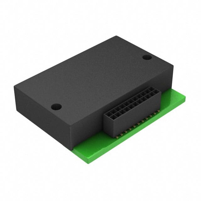
| 描述 | MODULE INERTIAL GYRO/ACCEL 24ML螺旋仪 4 Degree of Freedom Inertial Sensor |
| 产品分类 | |
| 品牌 | Analog Devices Inc |
| 产品手册 | |
| 产品图片 |
|
| rohs | RoHS 合规性豁免无铅 / 符合限制有害物质指令(RoHS)规范要求 |
| 产品系列 | 螺旋仪,Analog Devices ADIS16300AMLZiSensor™ |
| 数据手册 | |
| 产品型号 | ADIS16300AMLZ |
| PCN设计/规格 | |
| 产品种类 | 螺旋仪 |
| 传感器类型 | 陀螺仪和加速计 |
| 传感轴 | Triple |
| 加速 | +/- 3 g |
| 商标 | Analog Devices |
| 封装 | Bulk |
| 工厂包装数量 | 12 |
| 数字输出-总线接口 | SPI |
| 最大工作温度 | + 25 C |
| 最小工作温度 | - 40 C |
| 标准包装 | 1 |
| 灵敏度 | 0.0125 deg/s/LSB |
| 电源电压-最大 | 5.25 V |
| 电源电压-最小 | 4.75 V |
| 电源电流 | 42 mA |
| 系列 | ADIS16300 |
| 输出类型 | 数字 - SPI |


- 商务部:美国ITC正式对集成电路等产品启动337调查
- 曝三星4nm工艺存在良率问题 高通将骁龙8 Gen1或转产台积电
- 太阳诱电将投资9.5亿元在常州建新厂生产MLCC 预计2023年完工
- 英特尔发布欧洲新工厂建设计划 深化IDM 2.0 战略
- 台积电先进制程称霸业界 有大客户加持明年业绩稳了
- 达到5530亿美元!SIA预计今年全球半导体销售额将创下新高
- 英特尔拟将自动驾驶子公司Mobileye上市 估值或超500亿美元
- 三星加码芯片和SET,合并消费电子和移动部门,撤换高东真等 CEO
- 三星电子宣布重大人事变动 还合并消费电子和移动部门
- 海关总署:前11个月进口集成电路产品价值2.52万亿元 增长14.8%


PDF Datasheet 数据手册内容提取
Four Degrees of Freedom Inertial Sensor ADIS16300 FEATURES FUNCTIONAL BLOCK DIAGRAM 14-bit digital gyroscope with digital range scaling AUX_ AUX_ ADC DAC ±75°/sec, ±150°/sec, ±300°/sec settings TEMPERATURE Tri-axis, 14-bit digital accelerometer SENSOR CS ±3 g measurement range MEMS SCLK 13-bit pitch and roll incline calculations ANGSUELNASRO RRATE CALEIBARNADTION REOGUITSPTUETRS DIN 330 Hz bandwidth DIGITAL AND SPI SIGNAL PROCESSING INTERFACE DOUT 150 ms start-up time CONDITIONING AND Factory-calibrated sensitivity, bias, and axial alignment TRI-AXIS MEMS CONVERSION ACCELERATION T Digitally controlled bias calibration SENSOR Digitally controlled sample rate, up to 819.2 SPS ALARMS External clock input enables sample rates up to 1200 SPS MANPAOGWEEMRENT VCC Digitally controlled filtering SELF-TESTE CDOIGNTITRAOLL GND PADruiogxgiitlraiaallmryy ma dcaitgbivilteaa tlce oidnn psdueilttfi/-ootneu stmpt uotn itoring ADIS16300 RST DIO1 DIO2 DIO3 DIO4 07842-001 L Figure 1. Programmable power management Embedded temperature sensor SPI-compatible serial interface O Auxiliary, 12-bit ADC input and DAC output Single-supply operation: 4.75 V to 5.25 V 2000 g shock survivability Operating temperature range: −40°C to +85°C S APPLICATIONS Medical instrumentation Robotics B Platform control Navigation GENERAL DESCRIPTION O The ADIS16300 iSensor® is a complete inertial system that investment associated with discrete designs. All necessary includes a yaw rate gyroscope and tri-axis accelerometer. Each motion testing and calibration are part of the production sensor in the ADIS16300 combines industry-leading iMEMS® process at the factory, greatly reducing system integration time. technology with signal conditioning that optimizes dynamic Tight orthogonal alignment simplifies inertial frame alignment performance. The factory calibration characterizes each sensor in navigation systems. An improved SPI interface and register for sensitivity, bias, alignment, and linear acceleration (gyro bias). structure provide faster data collection and configuration control. As a result, each sensor has its own dynamic compensation for The ADIS16300, along with a flex interface, drops into current correction formulas that provide accurate sensor measurements systems that use the ADIS1635x family, providing the opportunity over the specified power supply range of +4.75 V to +5.25 V. to scale cost for systems that only require four degrees of The ADIS16300 provides a simple, cost-effective method for freedom inertial sensing. This compact module is approximately integrating accurate, multi-axis, inertial sensing into industrial 23 mm × 31 mm × 7.5 mm and provides a standard connector systems, especially when compared with the complexity and interface, which enables horizontal or vertical mounting. Rev. A Information furnished by Analog Devices is believed to be accurate and reliable. However, no responsibility is assumed by Analog Devices for its use, nor for any infringements of patents or other One Technology Way, P.O. Box 9106, Norwood, MA 02062-9106, U.S.A. rights of third parties that may result from its use. Specifications subject to change without notice. No license is granted by implication or otherwise under any patent or patent rights of Analog Devices. Tel: 781.329.4700 www.analog.com Trademarks and registered trademarks are the property of their respective owners. Fax: 781.461.3113 ©2008–2009 Analog Devices, Inc. All rights reserved.
ADIS16300 TABLE OF CONTENTS Features .............................................................................................. 1 Basic Operation .................................................................................9 Applications ....................................................................................... 1 Reading Sensor Data .....................................................................9 Functional Block Diagram .............................................................. 1 Device Configuration ...................................................................9 General Description ......................................................................... 1 Burst Mode Data Collection ........................................................9 Revision History ............................................................................... 2 Output Data Registers ............................................................... 11 Specifications ..................................................................................... 3 Calibration ................................................................................... 11 Timing Specifications .................................................................. 5 Operational Control ..............................E..................................... 12 Timing Diagrams .......................................................................... 5 Input/Output Functions ............................................................ 13 Absolute Maximum Ratings ............................................................ 6 Diagnostics .................................................................................. 14 ESD Caution .................................................................................. 6 Outline Dimensions ..............T......................................................... 16 Pin Configuration and Function Descriptions ............................. 7 Ordering Guide .......................................................................... 16 Typical Performance Characteristics ............................................. 8 E REVISION HISTORY 4/09—Rev. 0 to Rev. A L Changes to Figure 5 and Figure 6 ................................................... 7 Changes to Figure 7 .......................................................................... 8 Changes to Ordering Guide .......................................................... 16 O 10/08—Revision 0: Initial Version S B O Rev. A | Page 2 of 16
ADIS16300 SPECIFICATIONS T = −40°C to +85°C, VCC = 5.0 V, angular rate = 0°/sec, dynamic range = ±300°/sec, ±1 g, unless otherwise noted. A Table 1. Parameter Test Conditions Min Typ Max Unit GYROSCOPE Dynamic Range ±300 ±375 °/sec Initial Sensitivity T = 25°C, dynamic range = ±300°/sec 0.0495 0.05 0.0505 °/sec/LSB A T = 25°C, dynamic range = ±150°/sec 0.025 °/sec/LSB A T = 25°C, dynamic range = ±75°/sec 0.0125 E °/sec/LSB A Sensitivity Temperature Coefficient 400 ppm/°C Misalignment Reference to z-axis accelerometer, T = 25°C 0.1 Degrees A Axis-to-frame (package), T = 25°C ±0.5 Degrees A T Nonlinearity Best fit straight line 0.1 % of FS Initial Bias Error T = 25°C, ±1 σ ±3 °/sec A In-Run Bias Stability T = 25°C, 1 σ, SMPL_PRD = 0x01 0.007 °/sec A Angular Random Walk T = 25°C, 1 σ, SMPL_PRD = 0x01 E 1.9 °/√hr A Bias Temperature Coefficient 0.1 °/sec/°C Linear Acceleration Effect on Bias Any axis, 1 σ (MSC_CTRL Bit [7] = 1) 0.05 °/sec/g Voltage Sensitivity VCC = 4.75 V to 5.25 V 0.25 °/sec/V L Output Noise T = 25°C, ±300°/sec range, no filtering 1.1 °/sec rms A Rate Noise Density T = 25°C, f = 25 Hz, ±300°/sec, no filtering 0.038 °/sec/√Hz rms A 3 dB Bandwidth 330 Hz O Sensor Resonant Frequency 14.5 kHz Self-Test Change in Output Response ±300°/sec range setting ±696 ±1400 ±2449 LSB ACCELEROMETERS Each axis Dynamic Range ±3 ±3.6 g S Initial Sensitivity 25°C 0.594 0.6 0.606 mg/LSB Sensitivity Temperature Coefficient X axis and Y axis 250 ppm/°C Z axis 300 ppm/°C Misalignment Axis-to-axis, T = 25°C, Δ = 90° ideal ±0.25 Degrees B A Axis-to-frame (package), T = 25°C ±0.5 Degrees A Nonlinearity Best fit straight line ±0.3 % of FS Initial Bias Error T = 25°C, ±1 σ, X axis and Y axis ±60 mg A O TA = 25°C, ±1 σ, Z axis ±110 mg In-Run Bias Stability T = 25°C, 1 σ, X axis and Y axis 0.048 mg A T = 25°C, 1 σ, Z axis 0.054 mg A Velocity Random Walk T = 25°C, 1 σ, X axis and Y axis 0.118 m/sec/√hr A T = 25°C, 1 σ, Z axis 0.164 m/sec/√hr A Bias Temperature Coefficient X axis and Y axis 2.5 mg/°C Z axis 4.5 mg/°C Output Noise T = 25°C, no filtering, X axis and Y axis 5 mg rms A T = 25°C, no filtering, Z axis 7.5 mg rms A Noise Density T = 25°C, no filtering, X axis and Y axis 0.2 mg/√Hz rms A T = 25°C, no filtering, Z axis 0.3 mg/√Hz rms A 3 dB Bandwidth 330 Hz Sensor Resonant Frequency 5.5 kHz Self-Test Change in Output Response X axis and Y axis 500 1100 1700 LSB Z axis 90 450 860 LSB INCLINOMETER Sensitivity 0.044 °/LSB TEMPERATURE SENSOR Scale Factor T = 25°C output = 0x0000 0.14 °C/LSB A Rev. A | Page 3 of 16
ADIS16300 Parameter Conditions Min Typ Max Unit ADC INPUT Resolution 12 Bits Integral Nonlinearity ±2 LSB Differential Nonlinearity ±1 LSB Offset Error ±4 LSB Gain Error ±2 LSB Input Range 0 +3.3 V Input Capacitance During acquisition 20 pF DAC OUTPUT 5 kΩ/100 pF to GND E Resolution 12 Bits Relative Accuracy For Code 101 to Code 4095 ±4 LSB Differential Nonlinearity ±1 LSB Offset Error ±5T mV Gain Error ±0.5 % Output Range 0 +3.3 V Output Impedance 2 Ω E Output Settling Time 10 μs LOGIC INPUTS1 Input High Voltage, V 2.0 V INH Input Low Voltage, V L 0.8 V INL CS signal to wake up from sleep mode 0.55 V CS Wake-Up Pulse Width 20 μs Logic 1 Input Current, I V = 3.3 V O ±0.2 ±10 μA INH IH Logic 0 Input Current, I V = 0 V INL IL All Pins Except RST −40 −60 μA RST Pin −1 mA Input Capacitance, C S 10 pF IN DIGITAL OUTPUTS1 Output High Voltage, V I = 1.6 mA 2.4 V OH SOURCE Output Low Voltage, V I = 1.6 mA 0.4 V OL SINK B FLASH MEMORY Endurance2 10,000 Cycles Data Retention3 T = 85°C 20 Years J FUNCTIONAL TIMES4 Time until data is available Power-On Start-up Time Normal mode, SMPL_PRD ≤ 0x09 180 ms O Low power mode, SMPL_PRD ≥ 0x0A 245 ms Reset Recovery Time Normal mode, SMPL_PRD ≤ 0x09 55 ms Low power mode, SMPL_PRD ≥ 0x0A 120 ms Sleep Mode Recovery Time 2.5 ms Flash Memory Test Time Normal mode, SMPL_PRD ≤ 0x09 17 ms Low power mode, SMPL_PRD ≥ 0x0A 90 ms Automatic Self-Test Time 12 ms CONVERSION RATE SMPL_PRD = 0x01 to 0xFF 0.413 819.2 SPS Clock Accuracy ±3 % Sync Input Clock 1.2 kHz POWER SUPPLY Operating voltage range, VCC 4.75 5.0 5.25 V Power Supply Current Low power mode at 25°C 18 mA Normal mode at 25°C 42 mA Sleep mode at 25°C 500 μA 1 The digital I/O signals are driven by an internal 3.3 V supply, and the inputs are 5 V tolerant. 2 Endurance is qualified as per JEDEC Standard 22, Method A117, and measured at −40°C, +25°C, +85°C, and +125°C. 3 The retention lifetime equivalent is at a junction temperature (TJ) of 85°C as per JEDEC Standard 22, Method A117. Retention lifetime decreases with junction temperature. 4 These times do not include thermal settling and internal filter response times (330 Hz bandwidth), which may impact overall accuracy. Rev. A | Page 4 of 16
ADIS16300 TIMING SPECIFICATIONS T = 25°C, VCC = 5 V, unless otherwise noted. A Table 2. Normal Mode Low Power Mode (SMPL_PRD < 0x09) (SMPL_PRD > 0x0A) Burst Mode Parameter Description Min1 Typ Max Min1 Typ Max Min1 Typ Max Unit f 0.01 2.0 0.01 0.3 0.01 1.0 MHz SCLK t Stall period between data 9 75 1/f μs STALL SCLK t Read rate 40 100 us READRATE t Chip select to clock edge 48.8 48.8 E48.8 ns CS t DOUT valid after SCLK edge 100 100 100 ns DAV t DIN setup time before SCLK rising edge 24.4 24.4 24.4 ns DSU t DIN hold time after SCLK rising edge 48.8 48.8 48.8 ns DHD T t , t SCLK rise/fall times 5 12.5 5 12.5 5 12.5 ns SCLKR SCLKF t , t DOUT rise/fall times 5 12.5 5 12.5 5 12.5 ns DF DR t CS high after SCLK edge 5 5 5 ns SFS E t Input sync pulse width 5 μs 1 t Input sync to data ready output 600 μs 2 t Input sync period 833 μs 3 L 1Guaranteed by design and characterization, but not tested in production. TIMING DIAGRAMS O CS t t CS SFS 1 2 3 S4 5 6 15 16 SCLK t DAV DOUT MSB DB14 DB13 DB12 DB11 DB10 DB2 DB1 LSB B t t DSU DHD DIN W/R A6 A5 A4 A3 A2 D2 D1 LSB 07842-002 O Figure 2. SPI Timing and Sequence t READRATE t STALL CS SCLK 07842-003 Figure 3. Stall Time and Data Rate t 3 t 2 t 1 SYNC CLOCK (DIO4) REDAADTAY 07842-004 Figure 4. Input Clock Timing Diagram Rev. A | Page 5 of 16
ADIS16300 ABSOLUTE MAXIMUM RATINGS Table 3. Stresses above those listed under Absolute Maximum Ratings Parameter Rating may cause permanent damage to the device. This is a stress Acceleration rating only; functional operation of the device at these or any Any Axis, Unpowered 2000 g other conditions above those indicated in the operational Any Axis, Powered 2000 g section of this specification is not implied. Exposure to absolute VCC to GND −0.3 V to +6.0 V maximum rating conditions for extended periods may affect Digital Input Voltage to GND −0.3 V to +5.3 V device reliability. Digital Output Voltage to GND −0.3 V to VCC + 0.3 V Table 4. Package Characteristics E Analog Input to GND −0.3 V to +3.6 V Package Type θ θ Device Weight Operating Temperature Range −40°C to +85°C JA JC 24-Lead Module 39.8°C/W 14.2°C/W 16 grams Storage Temperature Range −65°C to +125°C1, 2 1 Extended exposure to temperatures outside the specified temperature T range of −40°C to +85°C can adversely affect the accuracy of the factory ESD CAUTION calibration. For best accuracy, store the parts within the specified operating range of −40°C to +85°C. 2 Although the device is capable of withstanding short-term exposure to 150°C, long-term exposure threatens internal mechanical integrity. E L O S B O Rev. A | Page 6 of 16
ADIS16300 PIN CONFIGURATION AND FUNCTION DESCRIPTIONS ADIS16300 TOP VIEW (Not to Scale) C D A DIO3 SCLK DIN DIO1 DIO2 VCC GND GND DNC DNC AUX_ DNC 1 3 5 7 9 11 13 15 17 19 21 23 2 4 6 8 10 12 14 16 18 20 22 24 N T S T C C D C C C C C O4/CLKI DOU C RS VC VC GN DN DN AUX_DA DN DN E DI NOTES 1. MATING CONNECTOR: SAMTEC FTSH-112-03 T 2 . DONRC E =Q UDIOV ANLOETN CTO.NNECT. 07842-005 Figure 5. Pin Configuration E a z SCREW HOLES (2x) ay L ax 27mm INTERFACE TO SYSTEM PCB USING g A RIBBON OR FLEX CABLE THAT HAS THE O YAW ADIS16300 MATING CONNECTOR INCLUDED. SADIS16300 SYSTEM PRINTED CIRCUIT BOARD PIN 1 07842-006 NOTES B 1. ACCELERATION (aX,aY,aZ) AND ROTATIONAL (gYAW) ARROWS INDICATE THE DIRECTION OF MOTION THAT PRODUCES A POSITIVE OUTPUT. Figure 6. Device Orientation, Mounting, and Interface Diagrams Table 5. Pin Function Descriptions Pin No. OMnemonic Type1 Description 1 DIO3 I/O Configurable Digital Input/Output. 2 DIO4/CLKIN I/O Configurable Digital Input/Output or Sync Clock Input. 16, 17, 18, 19, 22, 23, 24 DNC N/A Do Not Connect. 3 SCLK I SPI Serial Clock. 4 DOUT O SPI Data Output. Clocks output on SCLK falling edge. 5 DIN I SPI Data Input. Clocks input on SCLK rising edge. 6 CS I SPI Chip Select. 7 DIO1 I/O Configurable Digital Input/Output. 8 RST I Reset. 9 DIO2 I/O Configurable Digital Input/Output. 10, 11, 12 VCC S Power Supply. 13, 14, 15 GND S Power Ground. 20 AUX_DAC O Auxiliary, 12-Bit DAC Output. 21 AUX_ADC I Auxiliary, 12-Bit ADC Input. 1 S is supply, O is output, I is input, N/A is not applicable. Rev. A | Page 7 of 16
ADIS16300 TYPICAL PERFORMANCE CHARACTERISTICS 0.1 0.01 c) CE(°/se NCE(g) 0.001 AN +1σ RIA RI A Z AXIS A 0.01 V V N ALLAN MEAN TALLA 0.0001 X AND Y E OT –1σ OO AXES O R R 0.0010.1 1 10Tau (sec)100 1k 10k 07842-007 0.000010.1 FigEure1 8. AccIeNlTeTEroG1m0RAeTteIOr AN lTlaIM1n0E V0 (asreica)nce 1k 10k07842-008 Figure 7. Gyroscope Allan Variance L O S B O Rev. A | Page 8 of 16
ADIS16300 BASIC OPERATION The ADIS16300 is an autonomous sensor system that starts up ainfteerrt iiat lh mase aas vuarleimd penotw deart sau aptp al ys avmolptaleg er aatned o fb 8eg1i9n.2s pSrPoSd. uAcfitnegr 15 14 13UPP1E2R B1Y1TE10 9 8 7 6 5LOW4ER B3YTE2 1 0 07482-110 Figure 10. Output Register Bit Assignments each sample cycle, the sensor data loads into the output registers READING SENSOR DATA and DIO1 pulses, providing a new-data-ready control signal for driving system-level interrupt service routines. In a typical Although the ADIS16300 produces data independently, it oper- system, a master processor accesses the output data registers ates as an SPI slave device, which communicates with system through the SPI interface, using the hook-up shown in Figure 9. (master) processors using the 16-bit segments displayed in Table 6 provides a generic, functional description for each pin Figure 11. Individual register reads reEquire two 16-bit sequences. on the master processor. Table 7 describes the typical master The first 16-bit sequence provides the read command bit (R/W processor settings normally found in a configuration register = 0) and the target register address (A6…A0). The second and used for communicating with the ADIS16300. sequence transmits the register contents (D15…D0) on the T I/O LINES ARE COMPATIBLE WITH DOUT line. For example, if DIN= 0x0A00, then the content of 3.3V OR 5V LOGIC LEVELS XACCL_OUT shifts out on the DOUT line during the next 16-bit 5V VDD sequence. E 10 11 12 The SPI operates in full duplex mode, which means that the master SYSTEM PROCESSOR SS 6 CS ADIS16300 processor can read the output data from DOUT while using the SPI MASTER SPI SLAVE same SCLK pulses to transmit the next target address on DIN. SCLK 3 SCLK DLEVICE CONFIGURATION MOSI 5 DIN The user register memory map (see Table 8) identifies config- MISO 4 DOUT uration registers with either a W or R/W. Configuration commands O also use the bit sequence displayed in Figure 12. If the MSB is IRQ 7 DIO1 equal to 1, the last eight bits (DC7...DC0) in the DIN sequence 13 14 15 load into the memory address associated with the address bits S 07842-009 (inAt5o. .A.Ad0d)r.e Fsos rL eoxcaamtiopnle 0, xif2 t6h e(A DLIMN _=M 0AxAG111, Fu,p tpheern b 0yxt1e)F alto tahdes Figure 9. Electrical Hook-Up Diagram conclusion of the data frame. Table 6. Generic Master Processor Pin Names and Functions Most of the registers have a backup location in nonvolatile flash Pin Name Function B memory. The master processor must manage the backup SS Slave select function. Set GLOB_CMD[3] = 1 (DIN = 0xBE01) to execute a IRQ Interrupt request manual flash update (backup) operation, which copies the user MOSI Master output, slave input registers into their respective flash memory locations. This MISO MasOter input, slave output operation takes 50 ms and requires the power supply voltage SCLK Serial clock to be within the specified limit to complete properly. The FLASH_CNT register provides a running count of these events Table 7. Generic Master Processor SPI Settings for managing the long-term reliability of the flash memory. Processor Setting Description BURST MODE DATA COLLECTION Master The ADIS16300 operates as a slave. SCLK Rate ≤ 2 MHz1 Normal mode, SMPL_PRD[7:0] < 0x08. Burst mode data collection offers a more process-efficient CPOL = 1 Clock polarity. method for collecting data from the ADIS16300. In 10 CPHA = 1 Clock phase. sequential data cycles (each separated by one SCLK period), all MSB-First Bit sequence. nine output registers clock out on DOUT. This sequence starts 16-Bit Shift register/data length. when the DIN sequence is 0011 1110 0000 0000 (0x3E00). Next, the contents of each output register are output from DOUT, 1 For burst mode, SCLK rate ≤ 1 MHz. For low power mode, SCLK rate ≤ 300 kHz. starting with SUPPLY_OUT and ending with AUX_ADC (see The user registers provide addressing for all input/output Figure 12). The addressing sequence shown in Table 8 deter- operations on the SPI interface. Each 16-bit register has two mines the order of the outputs in burst mode. 7-bit addresses: one for its upper byte and one for its lower byte. Table 8 provides the lower-byte address for each register, and Figure 10 provides the generic bit assignments. Rev. A | Page 9 of 16
ADIS16300 Table 8. User Register Memory Map Name R/W Flash Backup Address1 Default Function Bit Assignments FLASH_CNT R Yes 0x00 N/A Flash memory write count N/A SUPPLY_OUT R No 0x02 N/A Power supply measurement Table 9 GYRO_OUT R No 0x04 N/A X-axis gyroscope output Table 9 N/A N/A N/A 0x06 N/A Reserved N/A N/A N/A N/A 0x08 N/A Reserved N/A XACCL_OUT R No 0x0A N/A X-axis accelerometer output Table 9 YACCL_OUT R No 0x0C N/A Y-axis accelerometer output Table 9 ZACCL_OUT R No 0x0E N/A Z-axis accelerometer output Table 9 E TEMP_OUT R No 0x10 N/A X-axis gyroscope temperature measurement Table 9 PITCH_OUT R No 0x12 N/A X-axis inclinometer output measurement Table 9 ROLL_OUT R No 0x14 N/A Y-axis inclinometer output measurement Table 9 AUX_ADC R No 0x16 N/A Auxiliary ADC output T Table 9 N/A N/A N/A 0x18 N/A Reserved N/A GYRO_OFF R/W Yes 0x1A 0x0000 X-axis gyroscope bias offset factor Table 10 N/A N/A N/A 0x1C N/A Reserved N/A E N/A N/A N/A 0x1E N/A Reserved N/A XACCL_OFF R/W Yes 0x20 0x0000 X-axis acceleration bias offset factor Table 11 YACCL_OFF R/W Yes 0x22 0x0000 Y-axis acceleration bias offset factor Table 11 ZACCL_OFF R/W Yes 0x24 0x0000 Z-axis acceLleration bias offset factor Table 11 ALM_MAG1 R/W Yes 0x26 0x0000 Alarm 1 amplitude threshold Table 22 ALM_MAG2 R/W Yes 0x28 0x0000 Alarm 2 amplitude threshold Table 22 ALM_SMPL1 R/W Yes 0x2A 0x0000 Alarm 1 sample size Table 23 O ALM_SMPL2 R/W Yes 0x2C 0x0000 Alarm 2 sample size Table 23 ALM_CTRL R/W Yes 0x2E 0x0000 Alarm control Table 24 AUX_DAC R/W No 0x30 0x0000 Auxiliary DAC data Table 18 GPIO_CTRL R/W No 0x32 0x0000 Auxiliary digital input/output control Table 16 S MSC_CTRL R/W Yes 0x34 0x0006 Miscellaneous control Table 17 SMPL_PRD R/W Yes 0x36 0x0001 Internal sample period (rate) control Table 13 SENS_AVG R/W Yes 0x38 0x0402 Dynamic range/digital filter control Table 15 SLP_CNT W No 0x3BA 0x0000 Sleep mode control Table 14 DIAG_STAT R No 0x3C 0x0000 System status Table 21 GLOB_CMD W N/A 0x3E 0x0000 System command Table 12 1 Each register contains two bytes. The aOddress of the lower byte is displayed. The address of the upper byte is equal to the address of the lower byte, plus 1. CS SCLK DIN R/W A6 A5 A4 A3 A2 A1 A0 DC7 DC6 DC5 DC4 DC3 DC2 DC1 DC0 R/W A6 A5 DOUT D15 D14 D13 D12 D11 D10 D9 D8 D7 D6 D5 D4 D3 D2 D1 D0 D15 D14 D13 N1.O DTOEUST BITS ARE BASED ON THE PREVIOUS 16-BIT SEQUENCE (R = 0). 07842-111 Figure 11. Output Register Bit Assignments CS 1 2 3 4 5 9 10 SCLK DIN 0x3E00 DON’T CARE DOUT PREVIOUS SUPPLY_OUT GYRO_OUT XACCL_OUT YACCL_OUT YINCL_OUT AUX_ADC 07842-012 Figure 12. Burst Mode Read Sequence Rev. A | Page 10 of 16
ADIS16300 OUTPUT DATA REGISTERS Auxiliary ADC Figure 6 provides the positive measurement direction for each The AUX_ADC register provides access to the auxiliary ADC inertial sensor (gyroscope and accelerometers). Table 9 provides input channel. The ADC is a 12-bit successive approximation the configuration and scale factor for each output data register converter, which has an equivalent input circuit to the one in in the ADIS16300. All inertial sensor outputs are 14-bits in Figure 14. The maximum input range is +3.3 V. The ESD length and are in twos complement format, which means that protection diodes can handle 10 mA without causing 0x0000 is equal to 0 LSB, 0x0001 is equal to +1 LSB, and 0x3FFF irreversible damage. The switch on-resistance (R1) has a typical is equal to −1 LSB. The following is an example of how to value of 100 Ω. The sampling capacitor, C2, has a typical value calculate the sensor measurement from the GYRO_OUT: of 16 pF. GYRO_OUT=0x3B4A VCC E 0x000−0x33B4A=−0x04B6=−(4×256+11×16+6) D R1 C2 −0x04B6=−1206LSB Rate=0.05°/sec×(−1206)=−60.3°/sec C1 TD 07842-011 Therefore, a GYRO_OUT output of 0x3B4A corresponds to a Figure 14. Equivalent Analog Input Circuit clockwise rotation about the z-axis (see Figure 6) of 60.3°/sec (Conversion Phase: Switch Open, Track Phase: Switch Closed) when looking at the top of the package. E CALIBRATION Table 9. Output Data Register Formats Manual Bias Calibration Register Bits Format Scale SUPPLY_OUT 12 Binary, 5 V = 0x0814 2.42 mV ThLe bias offset registers in Table 10 and Table 11 provide a manual GYRO_OUT1 14 Twos complement 0.05°/sec adjustment function for the output of each sensor. For example, XACCL_OUT 14 Twos complement 0.6 mg if GYRO_OFF equals 0x1FF6, the GYRO_OUT offset shifts by YACCL_OUT 14 Twos complement 0.6 mg O −10 LSBs, or −0.125°/sec. The DIN command for the upper ZACCL_OUT 14 Twos complement 0.6 mg byte is DIN = 0x9B1F; for the lower byte, DIN = 0x9AF6. TEMP_OUT 12 Twos complement 0.14°C Table 10. GYRO_OFF 25°C = 0x0000 Bits Description ROLL_OUT 13 Twos complement 0.044° S [15:13] Not used. PITCH_OUT 13 Twos complement 0.044° [12:0] Data bits. Twos complement, 0.0125°/sec per LSB. AUX_ADC 12 Binary, 1 V = 0x04D9 0.81 mV Typical adjustment range = ±50°/sec. 1 Assumes that the scaling is set to ± 300°/sec. This faBctor scales with the range. Table 11. XACCL_OFF, YACCL_OFF, ZACCL_OFF Each output data register uses the bit assignments shown in Bits Description Figure 13. The ND flag indicates that unread data resides in the [15:12] Not used. output data registers. This flag clears and returns to 0 during an [11:0] Data bits, twos complement 0.6 mg/LSB. output register read sequencOe. It returns to 1 after the next Typical adjustment range = ±1.2 g. internal sample updates the registers with new data. The EA flag Gyroscope Automatic Bias Null Calibration indicates that one of the error flags in the DIAG_STAT register (see Table 21) is active (true). The remaining 14-bits are for data. Set GLOB_CMD[0] = 1 (DIN = 0xBE01) to execute this function, which measures GYRO_OUT and then loads GYRO_OFF with MSB FOR 14-BIT OUTPUT the opposite value to provide a quick bias calibration. Then, all ND EA MSB FOR 12-BIT OUTPUT 07842-013 saeuntosomra dtiactaal lrye s(e5t0s mtos z).e rSoe,e a Tnadb tleh e1 2fl.a sh memory updates Figure 13. Output Register Bit Assignments Gyroscope Precision Automatic Bias Null Calibration Inclinometers Set GLOB_CMD[4] = 1 (DIN = 0xBE10) to execute this function, The ROLL_OUT and PITCH_OUT registers provide a tilt angle which takes the sensor offline for 30 seconds while it collects a calculation, based on the accelerometers. The zero reference is set of GYRO_OUT data and calculates a more accurate bias the point at which the z-axis faces gravity for a north-east-down correction factor. Once calculated, the correction factor loads (NED) configuration. into GYRO_OFF, all sensor data resets to zero, and the flash ⎛YACCL_OUT⎞ memory updates automatically (50 ms). See Table 12. ROLL_OUT=atan⎜ ⎟=φ ⎜ ⎟ ⎝ZACCL_OUT⎠ ⎛ −XACCL_OUT ⎞ PITCH_OUT=atan⎜ ⎟ ⎜⎝YACCL_OUT xsin(φ)+ZACCL_OUT xcos(φ)⎟⎠ Rev. A | Page 11 of 16
ADIS16300 Restoring Factory Calibration For example, set SMPL_PRD[7:0] = 0x0A (DIN = 0xB60A) for Set GLOB_CMD[1] = 1 (DIN = 0xBE02) to execute this function, an internal sample period of 6.7 ms (sample rate = 149 SPS). which resets each user calibration register (see Table 10 and For systems that value lower sample rates, in-system character- Table 11) to 0x0000, resets all sensor data to zero, and auto- ization can help determine performance trade-offs. matically updates the flash memory (50 ms). See Table 12. Power Management Linear Acceleration Bias Compensation (Gyroscope) Setting SMPL_PRD ≥ 0x0A also sets the sensor in low power Set MSC_CTRL[7] = 1 (DIN = 0xB486) to enable correction for mode. In addition to sensor performance, this mode also affects low frequency acceleration influences on gyroscope bias. Note SPI data rates (see Table 2). Two sleep mode options are listed that the DIN sequence also preserves the factory default condi- in Table 14. Set SLP_CNT[8] = 1 (DIN = 0xBB01) to start the tion for the data ready function (see Table 17). indefinite sleep mode, which requires CSE assertion (high to OPERATIONAL CONTROL low), reset, or power cycle to wake-up. Set SLP_CNT[7:0] = 0x64 (DIN = 0xBA64) to put the ADIS16300 to sleep for 100 Global Commands seconds, as an example of the programmable sleep time option. T The GLOB_CMD register provides trigger bits for several useful functions. Setting the assigned bit to 1 starts each operation, Table 14. SLP_CNT which returns to the bit to 0 after completion. For example, set Bit Description GLOB_CMD[7] = 1 (DIN = 0xBE80) to execute a software [15:9] Not usedE reset, which stops the sensor operation and runs the device [8] Indefinite sleep mode, set to 1 through its start-up sequence. This includes loading the control [7:0] Programmable time bits, 0.5 sec/LSB registers with their respective flash memory locations prior to DigitaLl Filtering producing new data. Reading the GLOB_CMD registers (DIN = The signal conditioning circuit of each sensor has a typical 0x3E00) starts the burst mode read sequence. analog bandwidth of 350 Hz. A programmable Bartlett window Table 12. GLOB_CMD OFIR filter provides an opportunity for additional noise reduction Bits Description on all output data registers. SENS_AVG[2:0] controls the [15:8] Not used number of taps according to the equation in Table 15. For [7] Software reset command example, set SENS_AVG[2:0] = 110 (DIN = 0xB806) to [6:5] Not used S establish a 129-tap setting. [4] Precision autonull command [3] Flash update command 0 [2] Auxiliary DAC data latch B [1] Factory calibration restore command –20 [0] Autonull command –40 Internal Sample Rate B) d The ADIS16300 performs best whOen the sample rate is set to the DE ( –60 U factory default setting of 819.2 SPS. For applications that value NIT –80 G lower sample rates, the SMPL_PRD register controls the A M ADIS16300 internal sample (see Table 13), and the following –100 relationship produces the sample rate: N = 5 –120 N = 9 t = t × N + 1 N = 33 S B S N = 129 –140 BTiatb le 13D. eSsMcrPipLt_iPonR D 0.001 0.01FREQUENCY (f/fS)0.1 1 07842-010 Figure 15. Bartlett Window FIR Frequency Response [15:8] Not used [7] Time base (t) B 0 = 0.61035 ms, 1 = 18.921 ms [6:0] Increment setting (N) S Internal sample period = t = t × N + 1 S B S Rev. A | Page 12 of 16
ADIS16300 Dynamic Range Data Ready I/O Indicator There are three dynamic range settings for the gyroscope: The factory default sets DIO1 as a positive data ready indicator ±75°/sec, ±150°/sec, and ±300°/sec. The lower dynamic range signal. The MSC_CTRL[2:0] register provides configuration settings (±75°/sec and ±150°/sec) limit the minimum filter tap options for changing this. For example, set MSC_CTRL[2:0] = sizes to maintain the resolution as the measurement range 100 (DIN = 0xB404) to change the polarity of the data ready decreases. The recommended order for programming the signal for interrupt inputs that require negative logic inputs for SENS_AVG register is upper byte (sensitivity), followed by activation. The pulse width will be between 100 μs and 200 μs lower byte (filtering). For example, set SENS_AVG[10:8] = 010 over all conditions. (DIN = 0xB902) for a measurement range to ±150°/sec. Table 17. MSC_CTRL Table 15. SENS_AVG Bits Description E Bits Value Description [15:12] Not used [15:11] Not used [11] Memory test (clears on completion) [10:8] Measurement range (sensitivity) selection 1 = enabled, 0 = disabled T 100 ±300°/sec (default condition) [10] Internal self-test enable (clears on completion) 010 ±150°/sec, filter taps ≥ 4 (Bits[2:0] ≥ 0x02) 1 = enabled, 0 = disabled 001 ±75°/sec, filter taps ≥ 16 (Bits[2:0] ≥ 0x04) [9] Manual self-test, negative stimulus E [7:3] Not used 1 = enabled, 0 = disabled [2:0] Filter tap setting, number of taps [8] Manual self-test, positive stimulus N = 2M+1 for M > 0, N = 1 for M = 0 1 = enabled, 0 = disabled [7L] Linear acceleration bias compensation for gyroscopes INPUT/OUTPUT FUNCTIONS 1 = enabled, 0 = disabled General-Purpose I/O [6] Linear accelerometer origin alignment DIO1, DIO2, DIO3, and DIO4 are configurable, general-purpose 1 = enabled, 0 = disabled O I/O lines that serve multiple purposes according to the following [5:3] Not used control register priority: MSC_CTRL, ALM_CTRL, and [2] Data ready enable GPIO_CTRL. For example, set GPIO_CTRL = 0x080C (DIN = 1 = enabled, 0 = disabled 0xB508, then 0xB40C) to set DIO1 and DIO2 as inputs and [1] Data ready polarity S 1 = active high, 0 = active low DIO3 and DIO4 as outputs, with DIO3 set low and DIO4 set high. [0] Data ready line select Table 16. GPIO_CTRL 1 = DIO2, 0 = DIO1 Bit Description B Auxiliary DAC [15:12] Not used The 12-bit AUX_DAC line can drive its output to within 5 mV [11] General-Purpose I/O Line 4 (DIO4) data level of the ground reference when it is not sinking current. As the [10] General-Purpose I/O Line 3 (DIO3) data level output approaches 0 V, the linearity begins to degrade (~100 LSB [9] General-Purpose I/OO Line 2 (DIO2) data level beginning point). As the sink current increases, the nonlinear [8] General-Purpose I/O Line 1 (DIO1) data level range increases. The DAC latch command moves the values of [7:4] Not used the AUX_DAC register into the DAC input register, enabling [3] General-Purpose I/O Line 4 (DIO4), direction control both bytes to take effect at the same time. 1 = output, 0 = input [2] General-Purpose I/O Line 3 (DIO3), direction control Table 18. AUX_DAC 1 = output, 0 = input Bit Description [1] General-Purpose I/O Line 2 (DIO2), direction control [15:12] Not used 1 = output, 0 = input [11:0] Data bits, scale factor = 0.8059 mV/code [0] General-Purpose I/O Line 1 (DIO1), direction control Offset binary format, 0 V = 0 codes 1 = output, 0 = input Input Clock Configuration Table 19. Setting AUX_DAC = 1V DIN Descripition The input clock configuration function allows for external 0XB0D9 AUX_DAC[7:0] = 0xD9 (217 LSB). control over sampling in the ADIS16300. Set GPIO_CTRL[3] = 0xB104 AUX_DAC[15:8] = 0x04 (1024 LSB). 0 (DIN = 0x0B200) and SMPL_PRD[7:0] = 0x00 (DIN = 0xBE04 GLOB_CMD[2] = 1. 0xB600) to enable this function. See Table 2 and Figure 4 for Move values into the DAC input register, resulting timing information. in a 1 V output level. Rev. A | Page 13 of 16
ADIS16300 DIAGNOSTICS Status Self-Test The error flags provide indicator functions for common system level issues. All of the flags clear (set to 0) after each DIAG_STAT Self-test offers the opportunity to verify the mechanical register read cycle. If an error condition remains, the error flag integrity of each MEMS sensor. It applies an electrostatic force returns to 1 during the next sample cycle. DIAG_STAT[1:0] to each sensor element, which results in mechanical displace- does not require a read of this register to return to zero. If the ment that simulates a response to actual motion. Table 1 lists power supply voltage goes back into range, these two flags clear the expected response for each sensor, which provides pass/fail automatically. criteria. Set MSC_CTRL[10] = 1 (DIN = 0xB504) to run the internal self-test routine, which exercises all inertial sensors, Table 21. DIAG_STAT Bit Descriptions measures each response, makes pass/fail decisions, and reports Bit Description E them to error flags in the DIAG_STAT register. MSC_CTRL[10] [15] Z-axis accelerometer self-test failure resets itself to 0 after completing the routine. MSC_CTRL[9:8] 1 = error condition, 0 = normal operation (DIN = 0xB502 or 0xB501) provides manual control over the [14] Y-axis accelerometer self-test failure self-test function. Table 20 gives an example test flow for using T 1 = error condition, 0 = normal operation this option. [13] X-axis accelerometer self-test failure 1 = error condition, 0 = normal operation Table 20. Manual Self-Test Example Sequence [12:11] Not usedE DIN Description [10] Gyroscope self-test failure 0xB601 SMPL_PRD[7:0] = 0x01, sample rate = 819.2 SPS. 1 = error condition, 0 = normal operation 0xB904 SENS_AVG[15:8] = 0x04, gyro range = ±300°/sec. [9] Alarm 2 status 0xB802 SENS_AVG[7:0] = 0x02, 4-tap averaging filter. L 1 = active, 0 = inactive Delay = 50 ms. [8] Alarm 1 status 0x0400 Read GYRO_OUT. 1 = active, 0 = inactive 0x0600 Read XACCL_OUT. O[7] Not used 0x0800 Read YACCL_OUT. [6] Flash test, check-sum flag 0x0A00 Read ZACCL_OUT. 1 = failure, 0 = normal operation 0xB502 MSC_CTRL[9] = 1, gyroscope negative self-test. [5] Self-test diagnostic error flag Delay = 50 ms. S 1 = error condition, 0 = normal operation 0x0400 Read GYRO_OUT. [4] Sensor overrange Determine whether the bias in the gyroscope 1 = error condition, 0 = normal operation output changes according to the expectation set [3] SPI communications failure in Table 2. B 1 = error condition, 0 = normal operation 0xB501 MSC_CTRL[9:8] = 01, gyroscope/accelerometer [2] Flash update failed positive self-test. 1 = error condition, 0 = normal operation Delay = 50 ms. [1] Power supply above 5.25 V 0x0400 Read GYRO_OUT. O 1 = power supply ≥ 5.25 V, 0 = power supply ≤ 5.25 V 0x0600 Read XACCL_OUT. [0] Power supply below 4.75 V 1 = power supply ≤ 4.75 V, 0 = power supply ≥ 4.75 V 0x0800 Read YACCL_OUT. 0x0A00 Read ZACCL_OUT Alarm Registers Determine whether the bias in the gyroscope and The alarm function provides monitoring for two independent accelerometers changed according to the expect- conditions. The ALM_CTRL register provides control inputs ation set in Table 2. for data source, data filtering (prior to comparison), static 0xB500 MSC_CTRL[15:8] = 0x00. comparison, dynamic rate-of-change comparison, and output Zero motion provides results that are more reliable. The settings indicator configurations. The ALM_MAGx registers establish the in Table 20 are flexible and provide opportunity for optimization trigger threshold and polarity configurations. around speed and noise influence. For example, lowering the Table 25 gives an example of how to configure a static alarm. filtering taps enables lower delay times but increases the oppor- tunity for noise influence. The ALM_SMPLx registers provide the numbers of samples to use in the dynamic rate-of-change configuration. The period Memory Test equals the number in the ALM_SMPLx register, multiplied by Setting MSC_CTRL[11] = 1 (DIN = 0xB508) does a check-sum the sample period time, established by the SMPL_PRD register. verification of the flash memory locations. The pass/fail criteria See Table 26 for an example of how to configure the sensor for load into the DIAG_STAT[6] register. this type of function. Rev. A | Page 14 of 16
ADIS16300 Table 22. ALM_MAG1, ALM_MAG2 Table 25. Alarm Configuration Example 1 Bit Description DIN Description [15] Comparison polarity 1 = greater than, 0 = less than 0xAF55 ALM_CTRL = 0x5517. 0xAE17 Alarm 1 input = XACCL_OUT. [14] Not used Alarm 2 input = XACCL_OUT. [13:0] Data bits that match the format of the trigger source Static level comparison, filtered data. selection DIO2 output indicator, positive polarity. Table 23. ALM_SMPL1, ALM_SMPL2 0xA783 ALM_MAG1 = 0x8341. 0xA641 Alarm 1 is true if XACCL_OUT > 0.5 g. Bit Description 0xA93C ALM_MAG2= 0x3CBF. [15:8] Not used E 0xA8BF Alarm 2 is true if XACCL_OUT < −0.5 g. [7:0] Data bits: number of samples (both 0x00 and 0x01 = 1) Table 26. Alarm Configuration Example 2 Table 24. ALM_CTRL Bit Designations DIN Description Bits Value Description T 0xAF76 ALM_CTRL = 0x7687. [15:12] Alarm 2 source selection 0xAE87 Alarm 1 input = ZACCL_OUT. 0000 Disable Alarm 2 input = YACCL_OUT. 0001 Power supply output ERate of change comparison, unfiltered data. 0010 Gyroscope output DIO2 output indicator, positive polarity. 0011 Not used 0xB601 SMPL_PRD = 0x0001. 0100 Not used Sample rate = 819.2 SPS. L 0101 X-axis accelerometer output 0xAB08 ALM_SMPL1 = 0x0008. 0110 Y-axis accelerometer output Alarm 1 rate of change period = 9.77 ms. 0111 Z-axis accelerometer output 0xAC50 ALM_SMPL2= 0x0050. 1000 Gyroscopes temperature output O Alarm 2 rate of change period = 97.7 ms. 1001 X-axis inclinometer output 0xA783 ALM_MAG1 = 0x8341. 1010 Y- axis inclinometer output 0xA641 Alarm 1 is true if XACCL_OUT > 0.5 g. 1011 Auxiliary ADC input 0xA93C ALM_MAG2= 0x3CBE. [11:8] Alarm 1 source selection (same as SAlarm 2) 0xA8BE Alarm 2 is true if XACCL_OUT < −0.5 g. [7] Rate of change (ROC) enable for Alarm 2 1 = rate of change, 0 = static level [6] Rate of change (ROC) enable for Alarm 1 1 = rate of change, 0 =B static level [5] Not used [4] Comparison data filter setting1 1 = filtered data, 0 = unfiltered data [3] Not used O [2] Alarm output enable 1 = enabled, 0 = disabled [1] Alarm output polarity 1 = active high, 0 = active low [0] Alarm output line select 1 = DIO2, 0 = DIO1 1 Incline outputs always use filtered data in this comparison. Rev. A | Page 15 of 16
ADIS16300 OUTLINE DIMENSIONS 31.254 31.000 30.746 13.60 13.60 13.50 13.50 13.40 13.40 E 23.254 2.20 THRU HOLE 23.000 (2 PLACES) 22.746 9.134 T 8.880 8.626 E 14.35 DETAIL A 12.70 TOP VIEW 7.18 L 7.20 MAX 6.424 O 1.27 3.05 6.170 5.916 0.64 1.754 END VIEW 1.500 S 1.246 1.27 BSC CONNECTOR PITCH DETAIL A B A 090308- Figure 16. 24-Lead Module with Connector Interface O (ML-24-4) Dimensions shown in millimeters ORDERING GUIDE Model Temperature Range Package Description Package Option ADIS16300AMLZ1 −40°C to +85°C 24-Lead Module with Connector Interface ML-24-4 1 Z = RoHS Compliant Part. ©2008–2009 Analog Devices, Inc. All rights reserved. Trademarks and registered trademarks are the property of their respective owners. D07842-0-4/09(A) Rev. A | Page 16 of 16