ICGOO在线商城 > 开发板,套件,编程器 > 评估板 - 传感器 > ADIS16209/PCBZ

 Datasheet下载
- 型号: ADIS16209/PCBZ
- 制造商: Analog
- 库位|库存: xxxx|xxxx
- 要求:
| 数量阶梯 | 香港交货 | 国内含税 |
| +xxxx | $xxxx | ¥xxxx |
查看当月历史价格
查看今年历史价格
ADIS16209/PCBZ产品简介:
ICGOO电子元器件商城为您提供ADIS16209/PCBZ由Analog设计生产,在icgoo商城现货销售,并且可以通过原厂、代理商等渠道进行代购。 ADIS16209/PCBZ价格参考¥932.43-¥932.43。AnalogADIS16209/PCBZ封装/规格:评估板 - 传感器, ADIS16209 iMEMS®, iSensor™ Accelerometer, Inclinometer, 2 Axis Sensor Evaluation Board。您可以下载ADIS16209/PCBZ参考资料、Datasheet数据手册功能说明书,资料中有ADIS16209/PCBZ 详细功能的应用电路图电压和使用方法及教程。
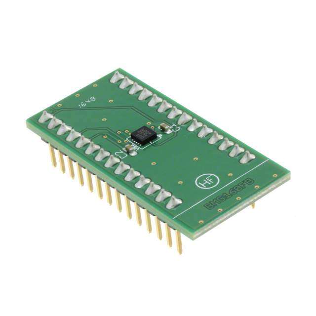
ADIS16209/PCBZ 是 Analog Devices Inc. 生产的一款评估板,专门用于评估 ADIS16209 数字倾斜传感器。该传感器主要用于测量静态倾斜角度和动态加速度,适用于多种应用场景,特别是在需要高精度、低噪声和宽温度范围的环境中。

 主要应用场景:

1. 工业自动化与机器人:
   - 在工业自动化系统中,ADIS16209/PCBZ 可以用于监测机器人的姿态和位置,确保其在复杂环境中的稳定性和精确性。例如,在装配线上的机械臂需要保持精确的姿态控制,以确保操作的准确性。

2. 建筑与结构健康监测:
   - 该评估板可以用于监测建筑物、桥梁等大型结构的倾斜角度,帮助工程师评估结构的安全性和稳定性。通过实时监控结构的微小变化,可以在潜在问题出现之前进行预警,避免事故发生。

3. 航空与航海设备:
   - 在航空和航海领域,ADIS16209/PCBZ 可以用于飞行器或船舶的姿态控制系统,确保其在恶劣环境下的稳定性和安全性。例如,无人机的自动驾驶系统依赖于精确的姿态感知,以实现平稳飞行和自动导航。

4. 医疗设备:
   - 在医疗设备中,特别是那些需要精确姿态控制的康复设备或手术辅助设备,ADIS16209/PCBZ 可以提供高精度的倾斜角度测量,帮助医生和患者更好地进行治疗和康复训练。

5. 农业机械:
   - 农业机械如联合收割机、拖拉机等在不平坦的地面上工作时,需要保持稳定的姿态以确保作业效率和安全。ADIS16209/PCBZ 可以帮助这些机械设备实时监测和调整姿态,确保其在不同地形上的稳定运行。

6. 运动与健身设备:
   - 在运动和健身设备中,如平衡训练器或智能跑步机,ADIS16209/PCBZ 可以用于监测用户的姿态和动作,提供实时反馈,帮助用户改进运动姿势,减少受伤风险。

总之,ADIS16209/PCBZ 评估板凭借其高精度、低功耗和广泛的温度适应性,适用于多种需要精确姿态测量和控制的应用场景,能够为各类设备提供可靠的数据支持。
| 参数 | 数值 |
| 产品目录 | 编程器,开发系统半导体 |
| 描述 | BOARD EVAL FOR ADIS16209加速传感器开发工具 ADIS16209 Eval Brd |
| 产品分类 | |
| 品牌 | Analog Devices Inc |
| 产品手册 | |
| 产品图片 |
|
| rohs | RoHS 合规性豁免不适用 / 不受限制有害物质指令(RoHS)规范要求限制 |
| 产品系列 | 传感器开发工具,加速传感器开发工具,Analog Devices ADIS16209/PCBZiMEMS®, iSensor™ |
| 数据手册 | |
| 产品型号 | ADIS16209/PCBZ |
| PCN设计/规格 | |
| 产品 | Development Kits |
| 产品培训模块 | http://www.digikey.cn/PTM/IndividualPTM.page?site=cn&lang=zhs&ptm=38http://www.digikey.cn/PTM/IndividualPTM.page?site=cn&lang=zhs&ptm=24711 |
| 产品目录页面 | |
| 产品种类 | 加速传感器开发工具 |
| 传感器类型 | 加速计,倾斜仪,2 轴 |
| 使用的IC/零件 | ADIS16209 |
| 其它名称 | ADIS16209PCBZ |
| 商标 | Analog Devices |
| 封装 | Bulk |
| 嵌入式 | 否 |
| 工厂包装数量 | 1 |
| 感应范围 | ±1.7g, ±90° |
| 所含物品 | 板 |
| 接口 | SPI 串行 |
| 标准包装 | 1 |
| 灵敏度 | 0.244mg/LSB, 0.025°/LSB |
| 电压-电源 | 3 V ~ 3.6 V |
| 相关产品 | /product-detail/zh/ADIS16209CCCZ/ADIS16209CCCZ-ND/1771158 |
| 配用 | /product-detail/zh/ADISUSBZ/ADISUSBZ-ND/1938210 |

.jpg)


- 商务部:美国ITC正式对集成电路等产品启动337调查
- 曝三星4nm工艺存在良率问题 高通将骁龙8 Gen1或转产台积电
- 太阳诱电将投资9.5亿元在常州建新厂生产MLCC 预计2023年完工
- 英特尔发布欧洲新工厂建设计划 深化IDM 2.0 战略
- 台积电先进制程称霸业界 有大客户加持明年业绩稳了
- 达到5530亿美元!SIA预计今年全球半导体销售额将创下新高
- 英特尔拟将自动驾驶子公司Mobileye上市 估值或超500亿美元
- 三星加码芯片和SET,合并消费电子和移动部门,撤换高东真等 CEO
- 三星电子宣布重大人事变动 还合并消费电子和移动部门
- 海关总署:前11个月进口集成电路产品价值2.52万亿元 增长14.8%


PDF Datasheet 数据手册内容提取
High Accuracy, Dual-Axis Digital Inclinometer and Accelerometer Data Sheet ADIS16209 FEATURES FUNCTIONAL BLOCK DIAGRAM Dual-mode inclinometer system AADUCX DAAUCX VREF Dual-axis, horizontal operation, ±90° ADIS16209 Single-axis, vertical operation, ±180° TEMPERATURE High accuracy, 0.1° SENSOR Digital inclination data, 0.025° resolution DUAL-AXIS CS Digital acceleration data, 0.244 mg resolution ACCELEROMETER SIGNAL CALIBRATION CONDITIONING AND ±1.7 g accelerometer measurement range CONVAENRDSION PRDOICGEITSASLING SPI SCLK Digital temperature sensor output PORT DIN Digitally controlled bias calibration SELF-TEST CDOIGNTITRAOLL DOUT Digitally controlled sample rate Digitally controlled frequency response Dual alarm settings with rate/threshold limits VDD Auxiliary digital I/O MANPAOGWEEMRENT ALARMS AUXII/LOIARY Digitally activated self-test GND Digitally activated low power mode SPI-compatible serial interface RST DIO1 DIO2 07096-001 Auxiliary 12-bit ADC input and DAC output Figure 1. Single-supply operation: 3.0 V to 3.6 V 3500 g powered shock survivability APPLICATIONS Platform control, stabilization, and alignment Tilt sensing, inclinometers, leveling Motion/position measurement Monitor/alarm devices (security, medical, safety) Navigation GENERAL DESCRIPTION The ADIS16209 is a high accuracy, digital inclinometer that Configurable operating parameters include sample rate, accommodates both single-axis (±180°) and dual-axis (±90°) power management, digital filtering, auxiliary analog and operation. The standard supply voltage (3.3 V) and serial digital output, offset/null adjustment, and self-test for sensor peripheral interface (SPI) enable simple integration into most mechanical structure. industrial system designs. A simple internal register structure The ADIS16209 is available in a 9.2 mm × 9.2 mm × 3.9 mm handles all output data and configuration features. This LGA package that operates over a temperature range of −40°C includes access to the following output data: calibrated to +125°C. It can be attached using standard RoHS-compliant acceleration, accurate incline angles, power supply, internal solder reflow processes. temperature, auxiliary analog and digital input signals, diagnostic error flags, and programmable alarm conditions. Rev. G Document Feedback Information furnished by Analog Devices is believed to be accurate and reliable. However, no responsibility is assumed by Analog Devices for its use, nor for any infringements of patents or other One Technology Way, P.O. Box 9106, Norwood, MA 02062-9106, U.S.A. rights of third parties that may result from its use. Specifications subject to change without notice. No license is granted by implication or otherwise under any patent or patent rights of Analog Devices. Tel: 781.329.4700 ©2008–2018 Analog Devices, Inc. All rights reserved. Trademarks and registered trademarks are the property of their respective owners. Technical Support www.analog.com
ADIS16209 Data Sheet TABLE OF CONTENTS Features .............................................................................................. 1 Typical Performance Characteristics ..............................................8 Applications ....................................................................................... 1 Theory of Operation ...................................................................... 10 Functional Block Diagram .............................................................. 1 Basic Operation .............................................................................. 11 General Description ......................................................................... 1 Output Data Registers ............................................................... 12 Revision History ............................................................................... 2 Operation Control Registers ..................................................... 14 Specifications ..................................................................................... 3 Calibration Registers .................................................................. 17 Timing Specifications .................................................................. 5 Alarm Registers .......................................................................... 17 Timing Diagrams .......................................................................... 5 Applications Information .............................................................. 19 Absolute Maximum Ratings ............................................................ 6 Power Supply Considerations ................................................... 19 Thermal Resistance ...................................................................... 6 Assembly ...................................................................................... 19 ESD Caution .................................................................................. 6 Interface Board ........................................................................... 20 Pin Configuration and Function Descriptions ............................. 7 Outline Dimensions ....................................................................... 21 Recommended Pad Geometry .................................................... 7 Ordering Guide .......................................................................... 21 REVISION HISTORY 8/2018—Rev. F to Rev. G Change to Note 5, Table 1 ................................................................ 4 7/2012—Rev. B to Rev. C Changes to Accelerometers Section ............................................. 12 Changes to Endnote 5 in Table 1 ..................................................... 4 Change to Digital Filtering Section .............................................. 14 Changed Digital Input/Output Voltage to GND Maximum Changes to Global Commands Section ....................................... 16 Rating from 5.5 V to 5.3 V ............................................................... 6 Changes to Assembly Section ....................................................... 19 Added 0x40 to 0x49 and 0x4A Addresses to Table 6 ................. 11 Added Figure 23; Renumbered Sequentially .............................. 19 Changes to Output Data Registers Section ................................ 12 Changes to Digital Filtering Section ............................................ 14 5/2017—Rev. E to Rev. F Changes to Self-Test Section ......................................................... 15 Changes to Figure 3 and Figure 4 ................................................... 5 Added Applications Information Section ................................... 18 Change to Basic Operation Section ............................................. 11 Updated Outline Dimensions ....................................................... 19 1/2015—Rev. D to Rev. E 8/2009—Rev. A to Rev. B Changes to Power Supply Considerations Section and Changes to Features Section ............................................................ 1 Assembly Section ............................................................................ 19 Changes to Input Low Voltage, VINL, Parameter, Table 1 .......... 4 Deleted VDD Ramp Rate Requirements Section and Transient Changes to Figure 18 and Figure 19............................................. 10 Current Demand from ADIS16209 Section ............................... 19 Changes to Table 7, Table 8, and Table 10 ................................... 12 Added Power-On Reset Function Section .................................. 19 Updated Outline Dimensions ....................................................... 16 Changes to Figure 23 ...................................................................... 20 Changes to Ordering Guide .......................................................... 16 6/2014—Rev. C to Rev. D 7/2008—Rev. 0 to Rev. A Changes to Table 2 ............................................................................ 5 Changes to Figure 19 ...................................................................... 10 Changes to Table 26 and Self-Test Section .................................. 15 Changes to Table 21 ....................................................................... 15 Changes to Status Section .............................................................. 18 Added Power Supply Considerations Section ............................ 19 3/2008—Revision 0: Initial Version Rev. G | Page 2 of 21
Data Sheet ADIS16209 SPECIFICATIONS T = 25°C, VDD = 3.3 V, tilt = 0°, unless otherwise noted. A Table 1. Parameter Test Conditions Min Typ Max Unit HORIZONTAL INCLINE Each axis Input Range ±90 Degrees Relative Accuracy ±30° from horizon, AVG_CNT = 0x08 ±0.1 Degrees Sensitivity ±30° from horizon 0.025 °/LSB VERTICAL ROTATION Rotational plane within ±30° of vertical Input Range −180 +180 Degrees Relative Accuracy 360° of rotation ±0.25 Degrees Sensitivity −40°C to +85°C 0.025 °/LSB ACCELEROMETER Each axis Input Range1 25°C ±1.7 g Nonlinearity1 Percentage of full scale ±0.1 ±0.2 % Alignment Error X sensor to Y sensor ±0.1 Degrees Cross Axis Sensitivity ±2 % Sensitivity −40°C to +85°C, VDD = 3.0 V to 3.6 V 0.243 0.244 0.245 mg/LSB ACCELEROMETER NOISE PERFORMANCE Output Noise AVG_CNT = 0x00 1.7 mg rms Noise Density AVG_CNT = 0x00 0.19 mg/√Hz rms ACCELEROMETER FREQUENCY RESPONSE Sensor Bandwidth 50 Hz Sensor Resonant Frequency 5.5 kHz ACCELEROMETER SELF-TEST STATE2 Output Change When Active At 25°C 706 1343 1973 LSB TEMPERATURE SENSOR Output at 25°C 1278 LSB Scale Factor −0.47 °C/LSB ADC INPUT Resolution 12 Bits Integral Nonlinearity (INL) ±2 LSB Differential Nonlinearity (DNL) ±1 LSB Offset Error ±4 LSB Gain Error ±2 LSB Input Range 0 2.5 V Input Capacitance During acquisition 20 pF ON-CHIP VOLTAGE REFERENCE 2.5 V Accuracy At 25°C −10 +10 mV Reference Temperature Coefficient ±40 ppm/°C Output Impedance 70 Ω DAC OUTPUT 5 kΩ/100 pF to GND Resolution 12 Bits Relative Accuracy For Code 101 to Code 4095 4 LSB Differential Nonlinearity 1 LSB Offset Error ±5 mV Gain Error ±0.5 % Output Range 0 to 2.5 V Output Impedance 2 Ω Output Settling Time 10 µs Rev. G | Page 3 of 21
ADIS16209 Data Sheet Parameter Test Conditions Min Typ Max Unit LOGIC INPUTS Input High Voltage, V 2.0 V INH Input Low Voltage, V 0.8 V INL Logic 1 Input High Current, I V = 3.3 V ±0.2 ±10 µA INH IH Logic 0 Input Low Current, I V = 0 V INL IL All Except RST −40 −60 μA RST3 −1 mA Input Capacitance, C 10 pF IN DIGITAL OUTPUTS Output High Voltage, V I = 1.6 mA 2.4 V OH SOURCE Output Low Voltage, V I = 1.6 mA 0.4 V OL SINK SLEEP TIMER Timeout Period4 0.5 128 Seconds START-UP TIME5 Time until data is available Power-On Fast mode, SMPL_PRD ≤ 0x07 150 ms Normal mode, SMPL_PRD ≥ 0x08 190 ms Reset Recovery Fast mode, SMPL_PRD ≤ 0x07 30 ms Normal mode, SMPL_PRD ≥ 0x08 70 ms Sleep Mode Recovery 2.5 ms FLASH MEMORY Endurance6 20,000 Cycles Data Retention7 T = 85°C 20 Years J CONVERSION RATE SETTING 1.04 2731 SPS POWER SUPPLY Operating Voltage Range 3.0 3.3 3.6 V Power Supply Current Normal mode, SMPL_PRD ≥ 0x08 11 14 mA Fast mode, SMPL_PRD ≤ 0x07 36 42 mA Sleep mode, −40°C to +85°C 140 350 µA 1 Guaranteed by iMEMS® packaged part testing, design, and/or characterization. 2 Self-test response changes as the square of VDD. 3 The RST pin has an internal pull-up. 4 Guaranteed by design. 5 The times presented in this section represent the time it takes to start producing data in the output registers, after the minimum VDD reaches 3.0 V. They do not represent the settling time of the internal filters. Note that for the default SENS_AVG and AVG_CNT settings, the typical settling time is ~1.28 seconds. For faster settling times, reduce the AVG_CNT and SMPL_PRD settings. Note that the trade-off associated with faster settling times is noise and power. 6 Endurance is qualified as per JEDEC Standard 22 Method A117 and measured at −40°C, +25°C, +85°C, and +125°C. 7 Retention lifetime equivalent at junction temperature (TJ) 55°C as per JEDEC Standard 22 Method A117. Retention lifetime decreases with junction temperature. Rev. G | Page 4 of 21
Data Sheet ADIS16209 TIMING SPECIFICATIONS T = 25°C, VDD = 3.3 V, tilt = 0°, unless otherwise noted. A Table 2. Parameter Description Min1 Typ Max Unit f Fast mode, SMPL_PRD ≤ 0x07 (f ≥ 546 Hz)2 0.01 2.5 MHz SCLK S Normal mode, SMPL_PRD ≥ 0x08 (f ≤ 482 Hz)2 0.01 1.0 MHz S t Chip select period, fast mode, SMPL_PRD ≤ 0x07 (f ≥ 546 Hz)2 32 μs DATARATE S Chip select period, normal mode, SMPL_PRD ≥ 0x08 (f ≤ 482 Hz)2 42 μs S t Chip select period, fast mode, SMPL_PRD ≤ 0x07 (f ≥ 546 Hz)2 10 μs STALL S Chip select period, normal mode, SMPL_PRD ≥ 0x08 (f ≤ 482 Hz)2 12 μs S t Chip select to clock edge 48.8 ns CS t Data output valid after SCLK edge 100 ns DAV t Data input setup time before SCLK rising edge 24.4 ns DSU t Data input hold time after SCLK rising edge 48.8 ns DHD t Data output fall time 5 12.5 ns DF t Data output rise time 5 12.5 ns DR t CS high after SCLK edge 5 ns SFS 1 Guaranteed by design, not tested. 2 Note that fS means internal sample rate. TIMING DIAGRAMS tDATARATE tSTALL CS SCLK tSTALL =tDATARATE – 16/fSCLK 07096-002 Figure 2. SPI Chip Select Timing CS tCS tSFS 1 2 3 4 5 6 15 16 SCLK tDAV DOUT MSB DB14 DB13 DB12 DB11 DB10 DB2 DB1 LSB tDSU tDHD DIN W/R A6 A5 A4 A3 A2 D2 D1 LSB 07096-003 Figure 3. SPI Timing (Utilizing SPI Settings Typically Identified as Phase = 1, Polarity = 1) DATA FRAME CS SCLK DIN W/R A6 A5 A4 A3 A2 A1 A0 DC7 DC6 DC5 DC4 DC3 DC2 DC1 DC0 WRERAITDE == 01 REGISTER ADDRESS DOND’ATT CAA FROER F WORR IRTEE ACDO CMOMMAMNDASNDS 07096-004 Figure 4. DIN Bit Sequence Rev. G | Page 5 of 21
ADIS16209 Data Sheet ABSOLUTE MAXIMUM RATINGS THERMAL RESISTANCE Table 3. Parameter Rating Table 4. Package Characteristics Acceleration (Any Axis, Unpowered) 3500 g Package Type θ θ Device Weight JA JC Acceleration (Any Axis, Powered) 3500 g 16-Terminal LGA 250°C/W 25°C/W 0.6 g VDD to GND −0.3 V to +7.0 V Digital Input/Output Voltage to GND −0.3 V to +5.3 V ESD CAUTION Analog Inputs to GND −0.3 to VDD + 0.3 V Analog Inputs to GND −0.3 to VDD + 0.3 V Operating Temperature Range −40°C to +125°C Storage Temperature Range −65°C to +150°C Stresses at or above those listed under Absolute Maximum Ratings may cause permanent damage to the product. This is a stress rating only; functional operation of the product at these or any other conditions above those indicated in the operational section of this specification is not implied. Operation beyond the maximum operating conditions for extended periods may affect product reliability. Rev. G | Page 6 of 21
Data Sheet ADIS16209 PIN CONFIGURATION AND FUNCTION DESCRIPTIONS C D D FE A X D N R U D G V A V 16 15 14 13 AY SCLK 1 12 AUX DAC AX PIN 1 INDICATOR DOUT 2 ADIS16209 11 DNC TOP LOOK THROUGH DIN 3 VIEW 10 DNC (Not to Scale) CS 4 9 RST 5 6 7 8 1 2 C C O O N N ID DI D D NOTES 1.DNC = DO NOT CONNECT TO THIS PIN. 2.TATHH LIRSAO YIUSOG UNHTO FTVR IAEONWM A T TCHHTAEUT AT RLOE PTP.O RTPEH SVISEIE NCWTO,S NB TFEHICGEAU PURISANET C ITOOHNNE FI SPIG IPNURSRO AAVTRIIDEOE NND OI FFT O TVRHIS EPI BCPLBAE CL KFARAYOGOMEU TITS HP LEUO RTOPOKOPES. DETSH.IS IS07096-005 Figure 5. Pin Configuration Table 5. Pin Function Descriptions Pin No. Mnemonic Type1 Description 1 SCLK I SPI, Serial Clock. 2 DOUT O SPI, Data Output. 3 DIN I SPI, Data Input. 4 CS I SPI, Chip Select. 5, 6 DIO1, DIO2 I/O Digital Input/Output Pins. 7, 8, 10, 11 DNC N/A Do not connect to this pin. 9 RST I Reset, Active Low. 12 AUX DAC O Auxiliary DAC Output. 13 VDD S Power Supply, 3.3 V. 14 AUX ADC I Auxiliary ADC Input. 15 VREF O Precision Reference. 16 GND S Ground. 1 S = supply; O = output; I = input. RECOMMENDED PAD GEOMETRY 4.1865 8× 2.6955 8× 0.670 12× 8.373 5.391 2× 4× 0.500 16× 1.127 9.2mm × 9.126m×m STACKED LGAPACKAGE 07096-006 Figure 6. Example of a Pad Layout Rev. G | Page 7 of 21
ADIS16209 Data Sheet TYPICAL PERFORMANCE CHARACTERISTICS 0.20 0.25 MAXIMUM 0.20 0.15 INCLINE ERROR 0.15 0.10 0.10 R (Degrees) 0.050 R (Degrees) 0.050 RRO–0.05 RRO–0.05 E E –0.10 –0.10 –0.15 –0.15 –0.20 –0.20–40 –30 –2I0NCLIN–A1T0ION A0NGLE (1D0egrees2)0 30 40 07096-018 –0.250 10R0OTATIONAL 2A0N0GLE (Degree3s0)0 400 07096-021 Figure 7. Horizontal Inclination Error (Eight Parts), Autonull at Horizontal Figure 10. Vertical Mode Rotational Error (Eight Parts), 25°C, 3.3 V Position, Stable Temperature, 3.3 V 0.3 0.3 0.2 0.2 0.1 ERROR (Degrees)–00..110 ERROR (Degrees)––00..210 –0.3 –0.2 –0.4 –0.3–60 –40 –20 TE0MPERA20TURE (4°0C) 60 80 10007096-019 –0.5–60 –40 –20 TE0MPERA20TURE (4°0C) 60 80 100 07096-022 Figure 8. Maximum Incline Error Over a ±30° Incline Range (Eight Parts) Over Figure 11. Vertical Mode Error (Eight Parts) vs. Temperature, 0° to 360°, 3.3 V Temperature, Autonull at Horizontal Position, 25°C, 3.3 V 0.15 0.3 0.2 0.10 0.1 0.05 ERROR (Degrees)–0.050 ERROR (Degrees)––00..210 –0.10 –0.3 –0.15 –0.4 –0.20 3.0 SUPPLY V3O.3LTAGE (V) 3.6 07096-020 –0.5 3.0 SUPPLY V3O.3LTAGE (V) 3.6 07096-023 Figure 9. Maximum Incline Error Over a ±30° Incline Range (Eight Parts) Over Figure 12. Vertical Mode Error (Eight Parts) vs. Supply Voltage, 0° to 360°, 25°C Supply Voltage, Autonull Horizontal Position, 25°C, 3.3 V Rev. G | Page 8 of 21
Data Sheet ADIS16209 30 3.5 VDD = 3.0V, 3.3V, 3.6V TEMP = –40°C, +25°C, +85°C %) 25 3.0 N ( O TI 2.5 LA 20 s) U e OP gre 2.0 OF P 15 R (De E O 1.5 G R TA 10 ER EN 1.0 C R PE 5 0.5 0 0 –0.50 –0.38 –0.26 S–E0N.1S4ITIV–I0T.0Y2 ERR0.O10R (%0).22 0.34 0.46 07096-013 0 10 20OFF3-0VERTI4C0AL TI5L0T (Deg60rees)70 80 90 07096-015 Figure 13. Accelerometer Output Sensitivity Error Distribution Figure 15. Error vs. Off-Vertical Tilt, 25°C, 3.3 V 20 VDD = 3.0V, 3.3V, 3.6V 18 TEMP = –40°C, +25°C, +85°C %) N ( 16 O TI 14 A L PU 12 O P F 10 O GE 8 A T N 6 E C ER 4 P 2 0 –6.0 –4.4 –2.8 B–IA1.S2 ERR0O.R4 (mg)2.0 3.6 5.2 07096-014 Figure 14. Accelerometer Output Bias Error Distribution Rev. G | Page 9 of 21
ADIS16209 Data Sheet THEORY OF OPERATION The ADIS16209 tilt sensing system uses gravity as its only stimulus, and a MEMS accelerometer as its sensing element. MEMS accelerometers typically employ a tiny, spring-loaded θx structure that is interlaced with a fixed pick-off finger structure. The spring constant of the floating structure determines how GRAVITY = 1g ax ftaor d iyt nmaomviecs fworhceens saussbojecciatetedd t ow iat hfo arcccee. lTerhaitsi ostnr uacntdu rteo rsetasptiocn ds θx HORIZON 07096-007 forces, such as gravity. Figure 16. Single-Axis Tilt Theory Diagram Figure 16 and Figure 17 illustrate how the accelerometer responds to gravity, according to its orientation, with respect ay to gravity. Figure 16 displays the configuration for the incline angle outputs, and Figure 17 displays the configuration used θx for the rotational angle position. This configuration provides greater measurement range than a single axis. The ADIS16209 ax itniocno ripntoor aatne si nthceli nsieg annagl lper, oacneds siitn cgo crirreccutsit f tohra ste cvoenravle krtnso awccne lera- θx HORIZON 07096-008 error sources that would otherwise degrade the accuracy level. Figure 17. Dual-Axis Tilt Theory Diagram 0° TILT 116 LEVEL PLANE 116 13 13 5 8 912 12 4 12 1 16 13 9 4 8 5 8 9 4 5 XYIINNCCLL__OOUUTT == 00°° 0Y°I N≤C XLI_NOCULT_O =U 0T° ≤ 90° X0°IN ≤C YLI_NOCULT_O =U 0T° ≤ 90° 07096-011 Figure 18. Horizontal Incline Angle Orientation GRA1gVITY 16209 16209 90261 90261 90261 90261 16209 16209 ROT_OUT 0° +30° +90° +120° +180° –150° –90° –60° XACCL_OUT –1g –0.866g 0g 0.5g +1g +0.866g 0g –0.5g YACCL_OUT 0g +0.5g +1g +0.866g 0g –0.5g –1g –0.866g 07096-012 NOTES 1. ROT_OUT = 180° IS 1 LSB DIFFERENT THAN ROT_OUT = –179.975°. Figure 19. Vertical Angle Orientation Rev. G | Page 10 of 21
Data Sheet ADIS16209 BASIC OPERATION The ADIS16209 requires only power/ground and SPI connec- EMBEDDED tions. The SPI is simple to hook up and is supported by many ADIS16209 PROCESSOR/ DSP/FPGA common digital hardware platforms. Figure 20 provides a CS PF simple hook-up diagram, while Table 2, Figure 2, and Figure 3 SCLK SCK provide timing and bit assignments. Figure 4 provides the bit DIN MOSI sfueqnucteinocne wfoitrh aicnc tehsesi nAgD tIhSe1 r6e2g0i9st hera sm itesm oowrny 1st6r-ubcittu, 2re-.b Eytaec hre g- DOUT MISO 07096-009 ister. Each byte has its own unique 7-bit address. Note that Figure 20. Typical SPI Hook-Up all 16 SCLK cycles are required for the DIN bit sequence to Many of the configuration registers have also been assigned configure the output for the next data frame. The ADIS16209 mirror locations in the flash memory, which effectively provide supports full duplex mode operation. Table 6 provides the them with a backup storage function. To ensure the backup of entire user register map for the ADIS16209. For each register, these registers, the COMMAND register provides an initiation the lower bytes address is given. For those registers that have bit for manual flash updates. The ENDURANCE register two bytes, the upper bytes address is simply the lower bytes provides a running count of these events. address, incremented by 0x01. Table 6. User Register Map Name R/W Flash Backup Address Size (Bytes) Function Reference ENDURANCE R Yes 0x00 2 Diagnostics, flash write counter (16-bit binary) SUPPLY_OUT R No 0x02 2 Output, power supply Table 18 XACCL_OUT R No 0x04 2 Output, x-axis acceleration Table 8 YACCL_OUT R No 0x06 2 Output, y-axis acceleration Table 9 AUX_ADC R No 0x08 2 Output, auxiliary ADC Table 20 TEMP_OUT R No 0x0A 2 Output, temperature Table 16 XINCL_OUT R No 0x0C 2 Output, ±90° x-axis inclination Table 11 YINCL_OUT R No 0x0E 2 Output, ±90° y-axis inclination Table 12 ROT_OUT R No 0x10 2 Output, ±180° vertical rotational position Table 14 XACCL_NULL R/W Yes 0x12 2 Calibration, x-axis acceleration offset null Table 30 YACCL_NULL R/W Yes 0x14 2 Calibration, y-axis acceleration offset null Table 30 XINCL_NULL R/W Yes 0x16 2 Calibration, x-axis inclination offset null Table 31 YINCL_NULL R/W Yes 0x18 2 Calibration, y-axis inclination offset null Table 31 ROT_NULL R/W Yes 0x1A 2 Calibration, vertical rotation offset null Table 31 0x1C to 0x1F 4 Reserved, do not write to these locations ALM_MAG1 R/W Yes 0x20 2 Alarm 1, amplitude threshold Table 32 ALM_MAG2 R/W Yes 0x22 2 Alarm 2, amplitude threshold Table 32 ALM_SMPL1 R/W Yes 0x24 2 Alarm 1, sample period Table 33 ALM_SMPL2 R/W Yes 0x26 2 Alarm 2, sample period Table 33 ALM_CTRL R/W Yes 0x28 2 Alarm, source control register Table 34 No 0x2A to 0x2F 6 Reserved AUX_DAC R/W No 0x30 2 Auxiliary DAC data Table 28 GPIO_CTRL R/W No 0x32 2 Operation, digital I/O configuration and data Table 27 MSC_CTRL R/W No 0x34 2 Operation, data-ready and self-test control Table 26 SMPL_PRD R/W Yes 0x36 2 Operation, sample rate configuration Table 22 AVG_CNT R/W Yes 0x38 2 Operation, filter configuration Table 24 SLP_CNT W Yes 0x3A 2 Operation, sleep mode control Table 23 STATUS R No 0x3C 2 Diagnostics, system status register Table 35 COMMAND W No 0x3E 2 Operation, system command register Table 29 No 0x40 to 0x49 10 Reserved PROD_ID R Yes 0x4A 2 Product identification = 0x3F51 N/A Rev. G | Page 11 of 21
ADIS16209 Data Sheet OUTPUT DATA REGISTERS The XACCL_OUT (see Table 8) and YACCL_OUT (see Table 9) registers provide access to acceleration data for each Table 7 provides the data configuration for each output data axis. For example, set DIN = 0x0400 to request data from the register in the ADIS16209. Starting with the MSB of the upper x-axis register on the next 16-bit SPI sequence. After reading byte, each output data register has the following bit sequence: the contents of one of these registers, mask off the upper two new data (ND) flag, error/alarm (EA) flag, followed by 14 data bits, convert the remaining 14-bit, twos complement number bits. The data bits are LSB justified, and in the case of the 12-bit into a decimal equivalent, and then multiply that number by data formats, the remaining two bits are not used. The ND flag 0.024414 to convert the measurement into units of acceleration indicates that unread data resides in the output data registers. (mg). Table 10 provides several examples of this data format. This flag clears and returns to 0 during an output register read sequence. It returns to 1 after the next internal sample update Table 8. XACCL_OUT (Base Address = 0x04), Read Only cycle completes. The EA flag indicates an error condition. The Bits Description STATUS register contains all of the error flags and provides the 15 New data bit = 1, when register contains un-read data ability to investigate the root cause. 14 Error/alarm = 1, when STATUS ≠ 0x0000 Table 7. Output Data Register Formats [13:0] x-axis accelerometer output data, twos complement, 1 LSB = 0.24414 mg, 0 g = 0x0000 Register Bits Format Scale1 SUPPLY_OUT 14 Binary, 3.3 V = 0x2A3D 0.30518 mV Table 9. YACCL_OUT (Base Address = 0x06), Read Only XACCL_OUT 14 Twos complement 0.24414 mg Bits Description YACCL_OUT 14 Twos complement 0.24414 mg 15 New data bit = 1, when register contains un-read data AUX_ADC 12 Binary, 2 V = 0x0CCC 0.6105 mV 14 Error/alarm = 1, when STATUS ≠ 0x0000 TEMP_OUT 12 Binary, 25°C = 0x04FE −0.47°C [13:0] y-axis accelerometer output data, twos complement, XINCL_OUT2 14 Twos complement 0.025° 1 LSB = 0.24414 mg, 0 g = 0x0000 YINCL_OUT2 14 Twos complement 0.025° ROT_OUT3 14 Twos complement 0.025° Table 10. Accelerometer Data Format Examples Acceleration (g) Decimal Hex Binary 1 Scale denotes quantity per LSB. +1.7 +6,963 0x1B33 xx01 1011 0011 0011 2 Range is −90° to +90°. 3 Range is −179.975° to +180°. +1.0 +4,096 0x1000 xx01 0000 0000 0000 +0.00048828 +2 0x0002 xx00 0000 0000 0010 Accelerometers +0.00024414 +1 0x0001 xx00 0000 0000 0001 The accelerometers respond to both static (gravity) and 0 0 0x0000 xx00 0000 0000 0000 dynamic acceleration using the polarity shown in Figure 21. −0.00024414 −1 0x3FFF xx11 1111 1111 1111 AY 0° TILT −0.00048828 −2 0xFFFE xx11 1111 1111 1110 AX 116 LEVEL PLANE −1.0 −4096 0x3000 xx11 0000 0000 0000 13 −1.7 −27,853 0xE4CD xx10 0100 1100 1101 12 4 5 8 9 XYIINNCCLL__OOUUTT == 00°° 07096-024 Figure 21. Accelerometer Polarity Rev. G | Page 12 of 21
Data Sheet ADIS16209 Horizontal Incline Angle Table 15. Vertical Incline Angle Data Format Examples Orientation Decimal Hex Binary The XINCL_OUT (see Table 11) and YINCL_OUT (see +180° − 0.025° +7,199 0x1C1F xx01 1100 0001 1111 Table 12) registers provide access to acceleration data for each +0.05° +2 0x0002 xx00 0000 0000 0010 axis. For example, set DIN = 0x0400 to request data from the +0.025° +1 0x0001 xx00 0000 0000 0001 x-axis register on the next 16-bit SPI sequence. After reading 0° 0 0x0000 xx00 0000 0000 0000 the contents of one of these registers, mask off the upper two −0.025° −1 0x3FFF xx11 1111 1111 1111 bits, convert the remaining 14-bit, twos complement number −0.05° −2 0x3FFE xx11 1111 1111 1110 into a decimal equivalent, and then multiply that number by −180° −7,200 0x23E0 xx10 0011 1110 0000 0.025 to convert the measurement into units of angle (°). Table 13 provides several examples of this data format. Internal Temperature Table 11. XINCL_OUT (Base Address = 0x0C), Read Only The TEMP_OUT register (see Table 16) provides access to an internal temperature measurement. Set DIN = 0x0A00 to Bits Description request the contents of this register. Mask off the upper four 15 New data bit = 1, when register contains un-read data bits, then convert the remaining 12-bit binary number into a 14 Error/alarm = 1, when STATUS ≠ 0x0000 decimal equivalent, subtract 1278, multiply it by −0.47 and add [13:0] x-axis inclinometer output data, twos complement, 0° = 0x0000, 1 LSB = 0.025°/LSB, ±90° range 25 to convert this number into °C. See Table 17 for examples of this format. Note that this internal temperature measurement Table 12. YINCL_OUT (Base Address = 0x0E), Read Only provides an indicator of condition changes, not an absolute Bits Description measurement of conditions outside of the package. 15 New data bit = 1, when register contains un-read data Table 16. TEMP_OUT (Base Address = 0x0A), Read Only 14 Error/alarm = 1, when STATUS ≠ 0x0000 Bits Description [13:0] y-axis inclinometer output data, twos complement, 0° = 0x0000, 1 LSB = 0.025°/LSB, ±90° range [15:0] Internal temperature data, binary format, sensitivity = −0.47°/LSB, 25°C = 1278 LSB = 0x04FE Table 13. Horizontal Incline Angle Data Format Examples Table 17. Internal Temperature Data Format Examples Orientation Decimal Hex Binary Temperature (°C) LSB Hex Binary +90° − 0.025° +3,599 0x0E0F 0000 1110 0000 1111 +0.05° +2 0x0002 xx00 0000 0000 0010 +125 1065 0x0429 xxxx 0100 0010 1001 +0.025° +1 0x0001 xx00 0000 0000 0001 25 + 0.47 1277 0x04FD xxxx 0100 1111 1101 0° 0 0x0000 xx00 0000 0000 0000 +25 1278 0x04FE xxxx 0100 1111 1110 −0.025° −1 0x3FFF xx11 1111 1111 1111 25 − 0.047 1279 0x04FF xxxx 0100 1111 1111 −0.05° −2 0x3FFE xx11 1111 1111 1110 0 1331 0x0533 xxxx 0101 0011 0011 −90° −3,600 0x31F1 xx11 0001 1111 0001 −40 1416 0x0588 xxxx 0101 1000 1000 Vertical Incline Angle Power Supply The ROT_OUT register (see Table 14) provides access to incline The SUPPLY_OUT register (see Table 18) provides a digital angle data for each axis. For example, set DIN = 0x1000 to measurement for the supply voltage on the VDD pins (see request data from this register on the next 16-bit SPI sequence. Figure 5). Set DIN = 0x0200 to request the contents of this register. See Table 19 for examples of this data format. After reading the contents of one of these registers, mask off the upper two bits, convert the remaining 14-bit, twos complement Table 18. SUPPLY_OUT (Base Address = 0x02), Read Only number into a decimal equivalent, and then multiply that Bits Description number by 0.025 to convert the measurement into units of 15 New data bit = 1, when register contains un-read data angle (°). Table 15 provides several examples of this data format. 14 Error/alarm = 1, when STATUS ≠ 0x0000 Table 14. ROT_OUT (Base Address = 0x10), Read Only [15:0] Power supply measurement data, binary format, 1 LSB = 0.00030518 V, 0 V = 0x0000 Bits Description 15 New data bit = 1, when register contains un-read data Table 19. Power Supply Data Format Examples 14 Error/alarm = 1, when STATUS ≠ 0x0000 Supply Level (V) LSB Hex Binary [13:0] Vertical inclinometer output data, twos complement, 3.6 11,796 0x2E14 xx10 1110 0001 0100 0° = 0x0000, 1 LSB = 0.025°/LSB, ±180° range 3.3 + 0.00030518 10,814 0x2A3E xx10 1010 0011 1110 3.3 10,813 0x2A3D xx10 1010 0011 1101 3.3 − 0.00030518 10,812 0x2A3C xx10 1010 0011 1100 3.0 9,830 0x2666 xx10 0110 0110 0110 Rev. G | Page 13 of 21
ADIS16209 Data Sheet Auxiliary ADC Table 23. SLP_CNT Bit Descriptions Bit Description (Default = 0x0000) The AUX_ADC register (see Table 20) provides a digital measurement for the AUX_ADC input pin (see Figure 5). 15:8 Not used Set DIN = 0x0800 to request the contents of this register. 7:0 Data bits, 0.5 seconds/LSB See Table 21 for examples of this data format. For example, writing 0x08 to the SLP_CNT register places the Table 20. AUX_ADC (Base Address = 0x08), Read Only ADIS16209 into sleep mode for 4 sec. The only way to stop this Bits Description process is to remove power or reset the device. 15 New data bit = 1, when register contains un-read data Digital Filtering 14 Error/alarm = 1, when STATUS ≠ 0x0000 The AVG_CNT register controls the moving average digital filter, [13:12] Not used which determines the size of the moving average filter in eight [15:0] Auxiliary ADC data, binary format, power-of-two step sizes (that is, 2M = 1, 2, 4, 16, 32, 64, 128, and 1 LSB = 0.0006105 V, 0 V = 0x0000 256). Filter setup requires one simple step: write the appropriate Table 21. Auxiliary ADC Data Format Examples M factor to the assigned bits in the AVG_CNT register. Note Supply Level (V) LSB Hex Binary that the default settings for AVG_CNT and SMPL_PRD provide 2.5 4095 0xFFF xxxx 1111 1111 1111 the best accuracy but require approximately 1.28 seconds to 0.001221 2 0x002 xxxx 0000 0000 0010 settle. 0.0006105 1 0x001 xxxx 0000 0000 0001 Table 24. AVG_CNT Bit Descriptions 0 0 0x000 xxxx 0000 0000 0000 Bit Description (Default = 0x0008) 15:4 Not used OPERATION CONTROL REGISTERS 3:0 Power-of-two step size, maximum binary value = 1000 Internal Sample Rate The following equation offers a frequency response relationship The SMPL_PRD register controls the ADIS16209 internal sample for this filter: rate and has two parts: a selectable time base and a multiplier. The sin(π×N×f ×t ) following relationship produces the sample rate: H (f)= S A N×sin(π×f ×t ) S t = t × N + 122.07 µs S B S 20 Table 22. SMPL_PRD Bit Descriptions N = 4 Bit Description (Default = 0x0014) 0 N = 16 15:8 Not used N = 128 7 Time base (t ): 0 = 244.14 µs, 1 = 7.568 ms B) –20 B d 6:0 Increment setting (N) E ( S D U –40 T An example calculation of the default sample period follows: NI G A SMPL_PRD = 0x01, B7 − B0 = 00000001 M –60 B7 = 0 → t = 244.14 µs, B6 … B0 = 000000001 → N = 1 B S –80 t = t × N + 122.07 µs = 244.14 × 1 + 122.07 = 366.21 µs S B S The sfaS m= p1l∕teS r=a t2e7 s3e1t tSinPgS has a direct impact on the SPI data –1000.001 0.01 f/fS 0.1 07096-010 rate capability. For sample rates ≥546 SPS, the SPI SCLK can Figure 22. Frequency Response—Moving Average Filter run at a rate up to 2.5 MHz. For sample rates <546 SPS, the SPI Digital I/O Lines SCLK can run at a rate up to 1 MHz. The sample rate setting The ADIS16209 provides two general-purpose, digital also affects power dissipation. When the sample rate is set to input/output lines that have several configuration options. <546 SPS, power dissipation typically reduces by a factor of 68%. The two different modes of operation offer a system- Table 25. Digital I/O Line Configuration Registers level trade-off between performance (sample rate, serial transfer Function Priority Register rate) and power dissipation. Data-Ready I/O Indicator 1 MSC_CTRL Power Management Alarm Indicator 2 ALM_CTRL In addition to offering two different performance modes for General-Purpose I/O Configuration 3 GPIO_CTRL power optimization, the ADIS16209 offers a programmable General-Purpose I/O Line Communication GPIO_CTRL shutdown period that the SLP_CNT register controls. Rev. G | Page 14 of 21
Data Sheet ADIS16209 Data-Ready I/O Indicator 1. Set AVG_CNT = 0x0000 and SMPL_PRD = 0x0008, to optimize the response times during the self-test transitions, The MSC_CTRL register provides controls for a data-ready while keeping the ADIS16209 in low power mode. In this function. For example, writing 0x05 to this register enables this configuration, the self-test response will be similar to a step function and establishes DIO2 as an active-low, data-ready line. response of a single-pole, low-pass filter that has a cutoff The duty cycle is 25% (±10% tolerance). frequency of 50 Hz. Table 26. MSC_CTRL Bit Descriptions 2. Read XACCL_OUT and YACCL_OUT. Bit Description (Default = 0x0000) 3. Set MSC_CTRL[8] = 1. 15:11 Not used 4. Delay > 20 ms, which provides the 50 Hz filter (internal to 10 Self-test at power-on: 1 = disabled, 0 = enabled ADIS16209) with at least six time constants to settle. 9 Not used 5. Read XACCL_OUT and YACCL_OUT. 8 Self-test enable: 1 = enabled, 0 = disabled 6. Calculate difference in measurements: 7:3 Not used • D-XACCL_OUT = XACCL_OUT (Step 6) − 2 Data-ready enable: 1 = enabled, 0 = disabled XACCL_OUT (Step 3) 1 Data-ready polarity: 1 = active high, 0 = active low • D-YACCL_OUT = YACCL_OUT (Step 6) − 0 Data-ready line select: 1 = DIO2, 0 = DIO1 YACCL_OUT (Step 3) 7. Set MSC_CTRL[8] = 0. 8. Restore the SMPL_PRD and AVG_CNT registers to their Self-Test operational values. The self-test function applies an electrostatic force to the MEMS 9. Determine normal operation by making sure that the structure, inside of the core sensor, which causes the structure D-XACCL_OUT and D-YACCL_OUT produced a change to move in a manner that simulates its response to gravity or of at least 350 LSB. linear acceleration. This provides an observable response in the accelerometer outputs that can serve as a validation of The 350 LSB pass/fail limit is approximately one-half of the data functional operation throughout the entire signal chain. The sheet specification for the minimum response time and is well MSC_CTRL register (Table 29) provides two different options above the noise floor. Because the purpose of this function is for using this function: manual (user-command) and automatic to identify gross functional issues, such as a zero response, this (during start-up/reset recovery). is a safe approach, given a stable platform and supply. When experiencing modest motion, some of the parameters may The manual self-test control is an on/off control for the need further consideration to account for application-specific electrostatic force. Set MSC_CTRL[8] = 1 to turn it on and set conditions. MSC_CTRL[8] = 0 to turn it off. For normal operation, this will be in the off state but this control bit provides an opportunity to activate it at any time, so that system processors can apply application-relevant pass/fail criteria to the responses. When MSC_CTRL[10] = 1, the automatic self-test process runs during the power-on process. This runs the ADIS16209 through on/off states for the self-test, while observing the difference in accelerometer response. This process concludes with a comparison of the differential response in each accelerometer, with internal pass/fail limits and a report of the result to STATUS[5]. Once the ADIS16209 completes is its start-up process, STATUS is available for a SPI-driven read, using DIN = 0x3C00 as the SPI input command (STATUS at Address 0x3C). Linear motion during the start-up process, VDD ramp rates/waveform and the tilt of the device can introduce uncertainty into the on/off levels and in some cases, cause a false failure report to STATUS[5] (result = 0x0020). While the selection of the pass/fail limits incorporates most conditions, false failures are still possible When presented with a self-test failure indication, where STATUS ≥ 0x0020, use the following process to test for basic function. This process assumes a stable power supply voltage and zero motion. Rev. G | Page 15 of 21
ADIS16209 Data Sheet General-Purpose I/O The software reset command restarts the internal processor, which loads all registers with the contents in their flash memory The GPIO_CTRL register controls the direction and data of the locations. general-purpose digital lines, DIO1 and DIO2. For example, writing a 0x02 to the GPIO_CTRL register sets DIO2 as an The flash update copies the contents of all the flash backup output line and DIO1 as an input line. Reading the data bits in registers into their assigned, nonvolatile flash memory loca- GPIO_CTRL reveals the line logic level. tions. This process takes approximately 50 ms and requires a power supply that is within the specified operating range. After Table 27. GPIO_CTRL Bit Descriptions waiting the appropriate time for the flash update to complete, Bit Description (Default = 0x0000) verify successful completion by reading the STATUS register (if 15:10 Not used successful, the flash update error is 0). If the flash update was 9 General-Purpose I/O Line 2 data not successful, reading this error bit accomplishes two things: it 8 General-Purpose I/O Line 1 data alerts the system processor to try again, and it clears the error 7:2 Not used flag, which is required for flash memory access. 1 General-Purpose I/O Line 2, data direction control: The DAC data latch command loads the contents of AUX_DAC 1 = output, 0 = input into the DAC latches. Because the AUX_DAC contents must be 0 General-Purpose I/O Line 1, data direction control: updated one byte at a time, this command ensures a stable DAC 1 = output, 0 = input output voltage during updates. Auxiliary DAC The autonull command provides a simple method for removing offset from the sensor outputs by taking the contents of the The auxiliary DAC provides a 12-bit level adjustment function. output data registers and loading the equal but opposite number The AUX_DAC register controls the operation of the auxiliary into the offset calibration registers. DAC function, which is useful for systems that require analog level controls. It offers a rail-to-rail buffered output that has a range To accomplish this, the autonull command executes the of 0 V to 2.5 V. The DAC can drive its output to within 5 mV of following operations: the ground reference when it is not sinking current. As the output 1. Read the XACCL_OUT, YACCL_OUT, XINCL_OUT, approaches ground, the linearity begins to degrade (100 LSB YINCL_OUT, and ROT_OUT values. beginning point). As the sink current increases, the nonlinear 2. Change the polarity of these measurements. range increases. The DAC output latch function, contained in 3. Write the results to the XACCL_NULL, YACCL_NULL, the COMMAND register, provides continuous operation while XINCL_NULL, YINCL_NULL, and ROT_NULL registers. writing to each byte of this register. The contents of this register 4. Perform a manual backup of all user registers, using the are volatile, which means that the desired output level must be flash memory bank. set after every reset and power cycle event. When using the horizontal incline angle measurements Table 28. AUX_DAC Bit Descriptions (XINCL_OUT and YINCL_OUT), the autonull helps remove Bit Description (Default = 0x0000) bias errors in the accelerometers, as well as orientation error, 15:12 Not used with respect to the horizontal plane (0 g). When using the 11:0 Data bits, scale factor = 0.6105 mV/code vertical incline measurement (ROT_OUT), do not use the Offset binary format, 0 V = 0 codes autonull function. The accuracy of this operation depends on stable inertial Global Commands conditions (zero acceleration or change in orientation, with The COMMAND register provides initiation bits for several respect to gravity) and optimal noise management during the commands that simplify many common operations. Writing a 1 measurement (see the Digital Filtering section). to the assigned COMMAND bit exercises its function. The factory calibration restore command sets the offset null registers (XACCL_NULL, for example) back to their default Table 29. COMMAND Bit Descriptions values. Bit Description (Default = 0x0000) 15:8 Not used 7 Software reset 6:5 Not used 4 Clear status register (reset all bits to 0) 3 Flash update; backs up all registers, see Table 6 2 DAC data latch 1 Factory calibration restore 0 Autonull Rev. G | Page 16 of 21
Data Sheet ADIS16209 CALIBRATION REGISTERS ALARM REGISTERS The ADIS16209 incorporates an extensive factory calibration The alarm function provides monitoring for two independent and provides precision acceleration, incline, and rotational conditions. The ALM_CTRL register provides control inputs position data. For systems that require on-site calibration, for data source, data filtering (prior to comparison), static/ user-programmable offset adjustment registers are available. dynamic, and output indicator configurations. The ALM_MAGx Table 30 provides the bit assignments for the following user- registers establish the trigger threshold and polarity configura- programmable calibration registers: XACCL_NULL and tions. The ALM_SMPLx registers provide the numbers of YACCL_NULL. Table 31 provides the bit assignments for samples to use in the dynamic rate-of-change configuration. the following user-programmable calibration registers: The rate-of-change calculation is XINCL_NULL, YINCL_NULL, and ROT_NULL. Y = 1 N∑DSy(n+1)−y(n)⇒Alarm⇒isY >or<M ? Table 30. Acceleration Offset Register Bit Designations C NDS n=1 C C Bit Description (Default = 0x0000) where: 15:14 Not used N is the number of samples in ALM_SMPLx. DS 13:0 Data bits, twos complement, sensitivity = 0.24414 mg/LSB y(n) is the sampled output data. M is the magnitude for comparison in ALM_MAGx. Table 31. Incline/Rotation Offset Register Bit Designations C > or < is determined by the MSB in ALM_MAGx. Bit Description (Default = 0x0000) 15:14 Not used Table 32. ALM_MAG1/ALM_MAG2 Bit Designations 13:0 Data bits, twos complement, sensitivity = 0.025°/LSB Bit Description (Default = 0x0000) 15 Comparison polarity: 1 = greater than, 0 = less than 14 Not used 13:0 Data bits, matches format of trigger source selection Table 33. ALM_SMPL1/ALM_SMPL2 Bit Designations Bit Description (Default = 0x0001) 15:8 Not used 7:0 Data bits: number of samples (both 0x00 and 0x01 = 1) Table 34. ALM_CTRL Bit Descriptions Bit Value Description (Default = 0x0000) 15:12 Trigger source, Alarm 2 0000 Disabled 0001 Power supply 0010 X-acceleration 0011 Y-acceleration 0100 Auxiliary ADC 0101 Temperature sensor 0110 X-axis incline angle 0111 Y-axis incline angle 1000 Rotational position 11:8 Trigger source, Alarm 1, same as Bits[15:12] 7 Not used 6 Alarm 2 rate-of-change control: 1 = enabled 5 Alarm 1 rate-of-change control: 1 = enabled 4 Alarm 2 filter: 1 = filtered data, 0 = no filter1 3 Alarm 1 filter: 1 = filtered data, 0 = no filter1 2 Alarm indicator, using DIO1/DIO2: 1 = enabled 1 Alarm indicator polarity: 1 = active high 0 Alarm indicator line select: 1 = DIO2, 0 = DIO1 1 Incline and vertical angles always use filtered data in this comparison. Rev. G | Page 17 of 21
ADIS16209 Data Sheet Status Table 35. STATUS Bit Descriptions The STATUS register provides a series of error flags that Bit Description (Default = 0x0000) provide indicator functions for common system-level issues. 15:10 Not used After reading the contents of this register, set COMMAND[4] = 9 Alarm 2 status: 1 = active, 0 = inactive 1 (DIN = 0xBE10) to reset all of its flags to zero. 8 Alarm 1 status: 1 = active, 0 = inactive 7:6 Not used 5 Self-test diagnostic error flag: 1 = error condition, 0 = normal operation 4 Not used 3 SPI communications failure: 1 = error condition, 0 = normal operation 2 Flash update failed: 1 = error condition, 0 = normal operation 1 Power supply greater than 3.625 V: 1 > 3.625 V, 0 ≤ 3.625 V (normal) 0 Power supply less than 2.975 V: 1 < 2.975 V, 0 ≥ 2.975 V (normal) Rev. G | Page 18 of 21
Data Sheet ADIS16209 APPLICATIONS INFORMATION POWER SUPPLY CONSIDERATIONS Filter Settling The ADIS16209 is a precision sensing system that uses an The SMPL_PRD and AVG_CNT settings have a direct impact embedded processor for critical interface and signal processing on the filter settling during turn-on. For example, when using functions. Supporting this processor requires a low impedance the default settings for these filters, the SUPPLY_OUT register power supply, which can manage transient current demands that takes approximately 1.28 seconds to settle. During this time, the happen during normal operation, as well as during the start-up SUPPLY_OUT register experiences a linear rise (assuming that process. Transient current demands start when the voltage on VDD is stable and greater than 3.0 V) and the low-voltage flag the VDD pin reaches ~2.1 V; therefore, it is important for the (STATUS[0]) is low. When the SUPPLY_OUT register reaches a voltage on the VDD pin to reach 3 V as quickly as possible. value that exceeds 2.975 V, the STATUS[0] flag automatically Linear VDD ramp profiles that reach 3 V in 100 µs provide lowers. reliable results when used in conjunction with design practices ASSEMBLY that support low dynamic source impedance. The ADP1712 is When developing a process flow for installing ADIS16209 a linear regulator that can support the recommended ramp profile. devices on PCBs, see the JEDEC standard document J-STD- See the ADIS1620x/21x/22x Power Regulator Suggestion page 020C for reflow temperature profile and processing information. for a reference design for using this regulator with the ADIS16209. The ADIS16209 can use the Sn-Pb eutectic process and the Pb- Power-On-Reset Function free eutectic process from this standard, with one exception: the The ADIS16209 has a power-on-reset (POR) function that peak temperature exposure is 240°C. For a more complete list of triggers a reset if the voltage on the VDD pin fails to transition assembly process suggestion, see the ADIS162xx LGA Assembly between 2.35 V and 2.7 V within 128 ms. Guidelines page at the Engineer Zone/MEMS Community website. Transient Current from VDD Ramp Rate Figure 23 provides an example pad layout for the location of the ADIS16209 on a printed circuit board (PCB). Because the ADIS16209 contains 2 μF of decoupling capacitance 1.178 BSC on VDD and some systems may use additional filtering (8 PLCS) capacitance, the VDD ramp rate will have a direct impact on initial transient current requirements. Use this formula to 0.670 BSC (12 PLCS) estimate the transient current, associated with a particular capacitance (C) and VDD ramp rate (dV/dt). 7.873 BSC i(t)=CdV (2 PLCS) dt 1.127 BSC (16 PLCS) For example, if VDD transitions from 0 V to +3.3 V in 33 µs, dinVte/rdnt aisl 2e qµuFa cl atop a1c0it0o0r0 (0nVo/ Sex (t3e.r3n Val/ 3ca3p µasc)i.t aWnchee)n, tchhea rcghianrgg itnhge 0(1.560 P0L BCSSC) 07096-123 current for this ramps rate is 200 mA, during the 33 µs ramp time. Figure 23. Example Pad Layout This relationship provides a tool for evaluating the initial charging currents against the current limit thresholds of system power supplies, which can cause power supply interruptions and the appearance of failed start-ups. This may also be important for maintaining surge current ratings of any series elements as well Rev. G | Page 19 of 21
ADIS16209 Data Sheet INTERFACE BOARD 00 1 1. The ADIS16209/PCBZ provides the ADIS16209 function on a 1.050 1.2 inch × 1.3 inch PCB, which simplifies the connection to an 2 ×0.925 existing processor system. The four mounting holes accommodate either M2 (2 mm) or Type 2-56 machine screws. These boards J1 J2 are made of IS410 material and are 0.063 inches thick. The second 2 ×0.673 U1 level assembly uses a SAC305-compatible solder composition iSensor (Pb-free), which has a presolder reflow thickness of approximately 0.005 inches. The pad pattern on the ADIS16209/PCBZ matches that shown in Figure 25. J1 and J2 are dual-row, 2 mm (pitch) connectors that work with a number of ribbon cable systems, C1 4 ×Ø0.087 including 3M Part Number 152212-0100-GB (ribbon-crimp M2×0.4 2 ×0.000 connector) and 3M Part Number 3625/12 (ribbon cable). J1/J2 PIN NUMBERS 0.150 1 2 J1 ADIS16209 J2 753 864 123 149 SCRCSSLTK DADIDAOCC2 11642 1131 0.200Figu0.035re 2 × 0.00025. PCB Assembly View and0.865 Dim2 × 0.900ensions 07096-026 2 5 9 10 4 DOUT DIO1 12 11 12 6 3 DIN DNC 7 10 10 DNC 7 10 13 8 VDD DNC 9 11 11 DNC 8 12 16 15 GND VREF 10 C1 1µF 4 2 7 5 8 59 07096-025 Figure 24. Electrical Schematic Rev. G | Page 20 of 21
Data Sheet ADIS16209 OUTLINE DIMENSIONS 5.391 BSC 9.35 2.6955 (4×) PIN1 BSC INDICATOR 9.20SQ (8×) 9.05 1.000BSC (16×) 13 16 12 1 8.373 BSC (2×) 0.797BSC (12×) 9 4 8 5 TOPVIEW 0.200 BOTTOMVIEW 0.373BSC MIN (16×) (ALLSIDES) 5.00 TYP 3.90 MAX SIDEVIEW 121409-C Figure 26. 16-Terminal Stacked Land Grid Array [LGA] (CC-16-2) Dimensions shown in millimeters ORDERING GUIDE Model1 Temperature Range Package Description Package Option ADIS16209CCCZ −40°C to +125°C 16-Terminal Stacked Land Grid Array [LGA] CC-16-2 ADIS16209/PCBZ Evaluation Board 1 Z = RoHS Compliant Part. ©2008–2018 Analog Devices, Inc. All rights reserved. Trademarks and registered trademarks are the property of their respective owners. D07096-0-8/18(G) Rev. G | Page 21 of 21
Mouser Electronics Authorized Distributor Click to View Pricing, Inventory, Delivery & Lifecycle Information: A nalog Devices Inc.: ADIS16209CCCZ ADIS16209/PCBZ