ICGOO在线商城 > 集成电路(IC) > 接口 - 模拟开关,多路复用器,多路分解器 > ADG772BCPZ-1REEL
 Datasheet下载
- 型号: ADG772BCPZ-1REEL
- 制造商: Analog
- 库位|库存: xxxx|xxxx
- 要求:
| 数量阶梯 | 香港交货 | 国内含税 |
| +xxxx | $xxxx | ¥xxxx |
查看当月历史价格
查看今年历史价格
ADG772BCPZ-1REEL产品简介:
ICGOO电子元器件商城为您提供ADG772BCPZ-1REEL由Analog设计生产,在icgoo商城现货销售,并且可以通过原厂、代理商等渠道进行代购。 ADG772BCPZ-1REEL价格参考¥8.52-¥8.52。AnalogADG772BCPZ-1REEL封装/规格:接口 - 模拟开关,多路复用器,多路分解器, 2 Circuit IC Switch 2:1 6.7Ohm (Typ) 12-LFCSP-WQ (3x3)。您可以下载ADG772BCPZ-1REEL参考资料、Datasheet数据手册功能说明书,资料中有ADG772BCPZ-1REEL 详细功能的应用电路图电压和使用方法及教程。
ADG772BCPZ-1REEL是Analog Devices Inc.生产的一款低电压、低功耗的单刀双掷(SPDT)模拟开关,属于接口类中的模拟开关/多路复用器产品。该器件采用1.8V至5.5V宽电源电压范围,适合电池供电设备,具有低导通电阻(典型值约4Ω)和快速开关速度,支持高频信号切换。

其主要应用场景包括便携式消费电子产品,如智能手机、平板电脑和可穿戴设备,用于音频信号路由、麦克风切换或传感器通道选择;在医疗仪器中,可用于低功耗信号采集系统中的多路生理信号切换;工业测量与数据采集系统中,适用于多通道传感器信号的轮询与切换;此外,在通信设备和测试仪器中也可用于实现模拟信号路径的动态控制。

该器件采用小型6引脚SC70封装,节省PCB空间,特别适合对尺寸和功耗敏感的应用。其CMOS工艺确保了低漏电流和高开关精度,适用于精密模拟信号处理环境。
| 参数 | 数值 |
| 产品目录 | 集成电路 (IC)半导体 |
| 描述 | IC MUX/DEMUX DUAL SPDT 12LFCSP模拟开关 IC 6.7 Ohm 3.6V CMOS 2:1 Mux/DMux USB 2.0 |
| DevelopmentKit | EVAL-ADG772EBZ |
| 产品分类 | |
| 品牌 | Analog Devices Inc |
| 产品手册 | |
| 产品图片 |
|
| rohs | 符合RoHS无铅 / 符合限制有害物质指令(RoHS)规范要求 |
| 产品系列 | 开关 IC,模拟开关 IC,Analog Devices ADG772BCPZ-1REEL- |
| 数据手册 | |
| 产品型号 | ADG772BCPZ-1REEL |
| PCN其它 | |
| 产品培训模块 | http://www.digikey.cn/PTM/IndividualPTM.page?site=cn&lang=zhs&ptm=16845 |
| 产品种类 | 模拟开关 IC |
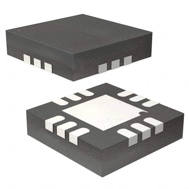
| 供应商器件封装 | 12-LFCSP-VQ (3x3) |
| 其它名称 | ADG772BCPZ-1REELCT |
| 功能 | 多路复用器/多路分解器 |
| 包装 | 剪切带 (CT) |
| 商标 | Analog Devices |
| 安装类型 | 表面贴装 |
| 安装风格 | SMD/SMT |
| 导通电阻 | 6.7 欧姆 |
| 封装 | Reel |
| 封装/外壳 | 12-VFQFN 裸露焊盘,CSP |
| 封装/箱体 | CSP-12 |
| 工作温度 | -40°C ~ 85°C |
| 工作电源电压 | 3.6 V |
| 工厂包装数量 | 5000 |
| 开关数量 | 2 |
| 开关电压—最大值 | 3.6 V |
| 开关电流—最大值 | 30 mA |
| 开关配置 | SPDT |
| 最大功率耗散 | 21.6 nW |
| 最大工作温度 | + 85 C |
| 最小工作温度 | - 40 C |
| 标准包装 | 1 |
| 电压-电源,单/双 (±) | 2.7 V ~ 3.6 V |
| 电压源 | 单电源 |
| 电流-电源 | 6nA |
| 电源电压-最大 | 3.6 V |
| 电源电压-最小 | 0 V |
| 电源电流—最大值 | 6 nA |
| 电路 | 2 x SPDT - NC/NO |
| 空闲时间—最大值 | 6 ns |
| 系列 | ADG772 |
| 运行时间—最大值 | 9 ns |


- 商务部:美国ITC正式对集成电路等产品启动337调查
- 曝三星4nm工艺存在良率问题 高通将骁龙8 Gen1或转产台积电
- 太阳诱电将投资9.5亿元在常州建新厂生产MLCC 预计2023年完工
- 英特尔发布欧洲新工厂建设计划 深化IDM 2.0 战略
- 台积电先进制程称霸业界 有大客户加持明年业绩稳了
- 达到5530亿美元!SIA预计今年全球半导体销售额将创下新高
- 英特尔拟将自动驾驶子公司Mobileye上市 估值或超500亿美元
- 三星加码芯片和SET,合并消费电子和移动部门,撤换高东真等 CEO
- 三星电子宣布重大人事变动 还合并消费电子和移动部门
- 海关总署:前11个月进口集成电路产品价值2.52万亿元 增长14.8%


PDF Datasheet 数据手册内容提取
CMOS Low Power Dual 2:1 Mux/Demux USB 2.0 (480 Mbps)/USB 1.1 (12 Mbps) Data Sheet ADG772 FEATURES FUNCTIONAL BLOCK DIAGRAM USB 2.0 (480 Mbps) and USB 1.1 (12 Mbps) signal ADG772 switching compliant S1A Tiny 10-lead 1.3 mm × 1.6 mm mini LFCSP package D1 S1B and 12-lead 3 mm × 3 mm LFCSP package 2.7 V to 3.6 V single-supply operation IN1 Typical power consumption: <0.1 μW IN2 RoHS compliant S2A APPLICATIONS D2 S2B UCeSlBlu 2la.0r spihgonnael ssw itching circuits SWITCHES SHOWN FOR A LOGIC 0 INPUT 06692-001 PDAs Figure 1. MP3 players Battery-powered systems Headphone switching Audio and video signal routing Communications systems GENERAL DESCRIPTION PRODUCT HIGHLIGHTS The ADG772 is a low voltage CMOS device that contains two 1. 1.6 mm × 1.3 mm mini LFCSP package. independently selectable single-pole, double throw (SPDT) 2. USB 1.1 (12 Mbps) and USB 2.0 (480 Mbps) compliant. switches. It is designed as a general-purpose switch and can be 3. Single 2.7 V to 3.6 V operation. used for routing both USB 1.1 and USB 2.0 signals. 4. 1.8 V logic compatible. 5. RoHS compliant. This device offers a data rate of 1260 Mbps, making the device suitable for high frequency data switching. Each switch con- ducts equally well in both directions when on and has an input signal range that extends to the supplies. The ADG772 exhibits break-before-make switching action. The ADG772 is available in a 12-lead LFCSP and a 10-lead mini LFCSP. These packages make the ADG772 the ideal solution for space-constrained applications. Rev. C Document Feedback Information furnished by Analog Devices is believed to be accurate and reliable. However, no responsibility is assumed by Analog Devices for its use, nor for any infringements of patents or other One Technology Way, P.O. Box 9106, Norwood, MA 02062-9106, U.S.A. rights of third parties that may result from its use. Specifications subject to change without notice. No license is granted by implication or otherwise under any patent or patent rights of Analog Devices. Tel: 781.329.4700 ©2007–2016 Analog Devices, Inc. All rights reserved. Trademarks and registered trademarks are the property of their respective owners. Technical Support www.analog.com
ADG772 Data Sheet TABLE OF CONTENTS Features .............................................................................................. 1 ESD Caution...................................................................................4 Applications ....................................................................................... 1 Pin Configuration and Function Descriptions ..............................5 Functional Block Diagram .............................................................. 1 Truth Table .....................................................................................5 General Description ......................................................................... 1 Typical Performance Characteristics ..............................................6 Product Highlights ........................................................................... 1 Test Circuits ........................................................................................9 Revision History ............................................................................... 2 Terminology .................................................................................... 11 Specifications ..................................................................................... 3 Outline Dimensions ....................................................................... 12 Absolute Maximum Ratings ............................................................ 4 Ordering Guide .......................................................................... 12 REVISION HISTORY 5/16—Rev. B to Rev. C Changes to Figure 3 .......................................................................... 5 Updated Outline Dimensions ....................................................... 12 Changes to Ordering Guide .......................................................... 12 4/13—Rev. A to Rev. B Added EPAD Notation .................................................................... 5 Changes to Figure 10 ........................................................................ 7 Updated Outline Dimensions ....................................................... 12 Changes to Ordering Guide .......................................................... 12 6/08—Rev. 0 to Rev. A Changes to Product Highlights ....................................................... 1 Changes to Input High Voltage, V , Parameter ......................... 3 INH 8/07—Revision 0: Initial Version Rev. C | Page 2 of 12
Data Sheet ADG772 Specifications V = 2.7 V to 3.6 V, GND = 0 V, unless otherwise noted. DD Table 1. Parameter +25°C −40°C to +85°C Unit Test Conditions/Comments ANALOG SWITCH Analog Signal Range 0 V to V V DD On-Resistance (R ) 6.7 Ω typ V = 2.7 V, V = 0 V to V , I = 10 mA; see Figure 21 ON DD S DD DS 8.8 Ω max On-Resistance Match 0.04 Ω typ V = 2.7 V, V = 1.5 V, I = 10 mA DD S DS Between Channels (∆R ) 0.2 Ω max ON On Resistance Flatness (R ) 3.3 Ω typ V = 2.7 V, V = 0 V to V , I = 10 mA FLAT (ON) DD S DD DS 3.6 Ω max LEAKAGE CURRENTS V = 3.6 V DD Source Off Leakage I (Off) ±0.2 nA typ V = 0.6 V/3.3 V, V = 3.3 V/0.6 V; see Figure 22 S S D Channel On Leakage I , I (On) ±0.2 nA typ V = V = 0.6 V or 3.3 V; see Figure 23 D S S D DIGITAL INPUTS Input High Voltage, V 1.35 V min INH Input Low Voltage, V 0.8 V max INL Input Current, I or I 0.005 µA typ V = V or V INL INH IN INL INH ±0.1 µA max V = V or V IN INL INH Digital Input Capacitance, C 2 pF typ IN DYNAMIC CHARACTERISTICS1 t 9 ns typ R = 50 Ω, C = 35 pF ON L L 12.5 13.5 ns max V = 2 V; see Figure 24 S t 6 ns typ R = 50 Ω, C = 35 pF OFF L L 9.5 10 ns max V = 2 V; see Figure 24 S Propagation Delay 250 ps typ R = 50 Ω, C = 35 pF L L Propagation Delay Skew, t 20 ps typ R = 50 Ω, C = 35 pF SKEW L L Break-Before-Make Time Delay (t ) 5 ns typ R = 50 Ω, C = 35 pF BBM L L 3.4 2.9 ns min V = V = 2 V; see Figure 25 S1 S2 Charge Injection 0.5 pC typ V = 1.25 V, R = 0 Ω, C = 1 nF; see Figure 26 D S L Off Isolation 73 dB typ R = 50 Ω, C = 5 pF, f = 1 MHz; see Figure 27 L L Channel-to-Channel Crosstalk −90 dB typ S1A to S2A/S1B to S2B; R = 50 Ω, C = 5 pF, L L f = 1 MHz; see Figure 28 −80 dB typ S1A to S1B/S2A to S2B; R = 50 Ω, C = 5 pF, L L f = 1 MHz; see Figure 29 −3 dB Bandwidth 630 MHz typ R = 50 Ω, C = 5 pF; see Figure 30 L L Data Rate 1260 Mbps typ R = 50 Ω, C = 5 pF; see Figure 30 L L C (Off) 2.4 pF typ S C , C (On) 6.9 pF typ D S POWER REQUIREMENTS V = 3.6 V DD I 0.006 µA typ Digital inputs = 0 V or 3.6 V DD 1 µA max 1 Guaranteed by design, not subject to production test. Rev. C | Page 3 of 12
ADG772 Data Sheet ABSOLUTE MAXIMUM RATINGS T = 25°C, unless otherwise noted. A Stresses at or above those listed under Absolute Maximum Ratings may cause permanent damage to the product. This is a Table 2. stress rating only; functional operation of the product at these Parameter Rating or any other conditions above those indicated in the operational V to GND −0.3 V to +4.6 V DD section of this specification is not implied. Operation beyond Analog Inputs,1 Digital Inputs −0.3 V to V + 0.3 V or DD 10 mA, whichever occurs first the maximum operating conditions for extended periods may Peak Current, Pin S1A, Pin S2A, 100 mA (pulsed at 1 ms, 10% affect product reliability. Pin D1, or Pin D2 duty cycle max) Only one absolute maximum rating can be applied at any Continuous Current, Pin S1A, 30 mA one time. Pin S2A, Pin D1, or Pin D2 ESD CAUTION Operating Temperature −40°C to +85°C Industrial Range (B Version) Storage Temperature Range −65°C to +150°C Junction Temperature 150°C θ Thermal Impedance JA (4-Layer Board) 10-Lead Mini LFCSP 131.6°C/W 12-Lead LFCSP 61°C/W Pb-Free Temperature, Soldering, IR Reflow Peak Temperature 260(+0/−5)°C Time at Peak Temperature 10 sec to 40 sec 1 Overvoltages at the IN1, IN2, S1A, S2A, D1, or D2 pin are clamped by internal diodes. Current must be limited to the maximum ratings given. Rev. C | Page 4 of 12
Data Sheet ADG772 PIN CONFIGURATION AND FUNCTION DESCRIPTIONS A1S DNG A2S 21 11 01 D11 9D2 ADG772 A1S D0NG A2S SN1BC32 (NToOt Pto V SIEcaWle) 78SN2CBB 1 1 9 4 5 6 D12 8D2 1N 2N DD ADG772 I I V S1B3 TOP VIEW 7S2B NOTES (Not to Scale) 1.NC = NO CONNECT. 2.THE EXPOSED PAD IS CONNECTED INTERNALLY. 1N4I 2N5I D6VD 006692-002 FJITSOOO RIR NAE TI CNGSOCR ARMONEMUDANE SMDNE ADRDXEE RIDFME ETULRHMIEAA NTBTHC ITLEEHITR.EYM POAALFD CT BHAEEP ASSBOOILLLDIDTEEYRR, EITD 06692-003 Figure 2. 10-Lead Mini LFCSP Pin Configuration Figure 3. 12-Lead LFCSP Pin Configuration Table 3. Pin Function Descriptions Pin No. 10-Lead Mini LFCSP 12-Lead LFCSP Mnemonic Description 1 12 S1A Source Terminal. Can be an input or an output. 2 1 D1 Drain Terminal. Can be an input or an output. 3 2 S1B Source Terminal. Can be an input or an output. 4 4 IN1 Logic Control Input. This pin controls Switch S1A and Switch S1B to D1. 5 5 IN2 Login Control Input. This pin controls Switch S2A and Switch S2B to D2. 6 6 VDD Most Positive Power Supply Potential. 7 8 S2B Source Terminal. Can be an input or an output. 8 9 D2 Drain Terminal. Can be an input or an output. 9 10 S2A Source Terminal. Can be an input or an output. 10 11 GND Ground (0 V) Reference. Not applicable 3, 7 NC No Connect. Not applicable 13 EPAD Exposed Pad. The exposed pad is connected internally. For increased reliability of the solder joints and maximum thermal capability, it is recommended that the pad be soldered to a ground reference. TRUTH TABLE Table 4. Logic (IN1 or IN2) Switch A (S1A or S2A) Switch B (S1B or S2B) 0 Off On 1 On Off Rev. C | Page 5 of 12
ADG772 Data Sheet TYPICAL PERFORMANCE CHARACTERISTICS 7 7 6 TA = 25°C VDD = 3.0V 6 TA = +85°C VDD = 3.3V VDD = 3.3V TA = +25°C Ω) 5 VDD = 3.6V Ω)5 E ( E ( NC 4 NC4 A A T T ESIS 3 ESIS3 TA = –40°C R R N N O O 2 2 1 1 00 0.5 1.0 1.5 VD, 2V.S0 (V) 2.5 3.0 3.5 4.0 06692-024 00 0.5 1.0 1V.5D, VS (V2).0 2.5 3.0 3.5 06692-027 Figure 4. On Resistance vs. VD, VS; VDD = 3.3 V ± 0.3 V Figure 7. On Resistance vs. VD, VS for Different Temperatures; VDD = 3.3 V 10 8 9 TA = 25°C VDD = 2.3V 7 VDD = 2.7V TA = +85°C 8 VDD = 2.5V 6 TA = +25°C Ω) 7 VDD = 2.7V Ω) CE ( 6 CE (5 N N A A N RESIST 54 N RESIST43 TA = –40°C O 3 O 2 2 1 1 00 0.5 1.0 1V.5D, VS (V2).0 2.5 3.0 3.5 06692-023 00 0.5 1.0 VD, 1V.S5 (V) 2.0 2.5 3.0 06692-026 Figure 5. On Resistance vs. VD, VS; VDD = 2.5 V ± 0.2 V Figure 8. On Resistance vs. VD, VS for Different Temperatures; VDD = 2.7 V 30 25 TA = 25°C VDD = 1.8V TA = –40°C 25 VDD = 1.65V 20 TA = +25°C ANCE (Ω)20 VDD = 1.8V NCE (Ω)15 TA = +85°C ST15 TA ESI VDD = 1.95V SIS ON R10 N RE10 O 5 5 00 0.2 0.4 0.6 0.8VD, 1V.S0 (V)1.2 1.4 1.6 1.8 2.0 06692-022 00 0.2 0.4 0.6 0.8VD, 1V.S0 (V)1.2 1.4 1.6 1.8 2.0 06692-025 Figure 6. On Resistance vs. VD, VS; VDD = 1.8 V ± 0.15 V Figure 9. On Resistance vs. VD, VS for Different Temperatures; VDD = 1.8 V Rev. C | Page 6 of 12
Data Sheet ADG772 1.2 2.0 VDD = 3.3V TA = 25°C 1.0 1.5 VCC = 3.3V 0.8 ID, IS (ON)++ 1.0 VCC = 2.5V A) T (n0.6 ID, IS (OFF)+– pC) RREN0.4 Q (INJ0.5 VCC = 1.8V U C 0 0.2 –0.5 0 –0.20 10 20 30TEMP4E0RATUI5DR0,E IS ( °(CO6)F0F)–+70ID, IS 8(0ON)––90 06692-028 –10 0.5 1.0 1.5VS (V)2.0 2.5 3.0 3.5 06692-018 Figure 10. Leakage Current vs. Temperature; VDD = 3.3 V Figure 13. Charge Injection vs. Source Voltage 0.9 12 VDD = 2.5V 0.8 0.7 10 tON(1.8V) 0.6 ID, IS (ON)++ tOFF (1.8V) tON(3.3V) 8 RENT (nA)00..54 ID, IS (ON)–– ME (ns) 6 tON(2t.7OVF)F (2.7V) CUR0.3 ID, IS (OFF)+– TI tOFF (3.3V) 4 0.2 0.1 2 0 ID, IS (OFF)–+ –0.10 10 20 30TEMP4E0RATU5R0E (°C)60 70 80 90 06692-029 0–40 –20 0TEMPER20ATURE (°4C0) 60 8085 06692-019 Figure 11. Leakage Current vs. Temperature; VDD = 2.5 V Figure 14. tON/tOFF Times vs. Temperature 0.8 0 VDD = 1.8V 0.7 –2 TA = 25°C 0.6 –4 VDD = 3.3V, 2.5V, 1.8V 0.5 ID, IS (ON)++ dB) –6 A) S ( n S ENT (0.4 N LO –8 URR0.3 ID, IS (ON)–– RTIO–10 C E 0.2 S–12 N I 0.1 –14 ID, IS (OFF)+– 0 –16 ID, IS (OFF)–+ –0.10 10 20 30TEMP4E0RATU5R0E (°C)60 70 80 90 06692-030 –18 1 FRE10QUENCY (M1H00z) 1000 06692-014 Figure 12. Leakage Current vs. Temperature; VDD = 1.8 V Figure 15. Bandwidth Rev. C | Page 7 of 12
ADG772 Data Sheet 0 TA = 25°C –10 VDD = 3.3V, 2.5V, 1.8V –20 B)–30 d N (–40 O ATI–50 U N E–60 T T A –70 2 –80 –90 –100 1 FRE10QUENCY (M1H00z) 1000 06692-016 C2 835mV Ω 22A0.5C.0G1nSs//sD E2IV.T6 44V00ps/pt 06692-021 Figure 16. Off Isolation vs. Frequency Figure 19. USB 1.1 Eye Diagram 0 +500mV 1 TA = 25°C –10 VDD = 3.3V, 2.5V, 1.8V –20 –30 B) K (d–40 +100mDVIV/ TAL–50 S1A to S1B 2 S S O–60 CR S1A to S2A –70 –80 –90 –100 1 FRE10QUENCY (M1H00z) 1000 06692-015 –500m3V7.373ns 250ps/DIV 39.87ns 06692-020 Figure 17. Crosstalk vs. Frequency Figure 20. USB 2.0 Eye Diagram 0 TA = 25°C VDD = 3.3V –20 –40 B)–60 d R ( R PS–80 –100 –120 –14010 100 1k F1R0EkQUE1N0C0Yk (MH1zM) 10M 100M 1G 06692-017 Figure 18. PSRR vs. Frequency Rev. C | Page 8 of 12
Data Sheet ADG772 TEST CIRCUITS IDS V1 S D VS RON = V1/IDS 06692-004 Figure 21. On Resistance IS(OFF) ID(OFF) S D A A VS VD 06692-005 Figure 22. Off Leakage ID(ON) S D NC A VD 06692-006 Figure 23. On Leakage VDD 0.1µF VDD VS SS11BA D VOUT VIN 50% 50% RL CL IN 50Ω 35pF 90% 90% VOUT GND tON tOFF 06692-007 Figure 24. Switching Times, tON, tOFF VDD 0.1µF 50% 50% VDD VIN 0V VS SS11BA D VOUT VOUT 80% 80% RL CL IN 50Ω 35pF t t BBM BBM GND 06692-008 Figure 25. Break-Before-Make Time Delay, tBBM VDD SWITCH ON SWITCH OFF VIN S1B NC D VS S1A VOUT 1nF IN VOUT ∆VOUT GND QINJ = CL × ∆VOUT 06692-009 Figure 26. Charge Injection Rev. C | Page 9 of 12
ADG772 Data Sheet VDD VDD 0.1µF 0.1µF NETWORK NETWORK VDD ANALYZER VDD ANALYZER NC S1B S1A 50Ω 50Ω VS S1B S1A 50Ω VS D D GND R50LΩVOUT GND R50LΩVOUT OFF ISOLATION = 20 logVVOSUT 06692-010 INSERTION LOSS = 20 logVOVUOTU WT IWTHITOHU STW SIWTCITHCH 06692-012 Figure 27. Off Isolation Figure 29. Channel-to-Channel Crosstalk (S1A to S1B) NETWORK VDD ANALYZER 0.1µF VOUT D2 50Ω S2A NC NETWORK S2B ANALYZER VDD S1A VOUT S1A D1 RL 50Ω 50Ω VS S1B NC 50Ω S1B D R50LΩ 50Ω CHANNEL-TO-CHANNEL CROSSTALK = 20 logVVOSUT 06692-013 VS GND Figure 28. Channel-to-Channel Crosstalk (S1A to S2A) CHANNEL-TO-CHANNEL CROSSTALK = 20 logVVOSUT 06692-011 Figure 30. Bandwidth Rev. C | Page 10 of 12
Data Sheet ADG772 TERMINOLOGY I C DD IN Positive supply current. Digital input capacitance. V ,V t D S ON Analog voltage on Terminal D and Terminal S. Delay time between the 50% and 90% points of the digital input and switch on condition. R ON Ohmic resistance between Terminal D and Terminal S. t OFF Delay time between the 50% and 90% points of the digital input R (On) FLAT and switch off condition. The difference between the maximum and minimum values of on resistance as measured on the switch. t BBM On or off time measured between the 80% points of both ∆R ON switches when switching from one to another. On resistance match between any two channels. Charge Injection I (Off) S Measure of the glitch impulse transferred from the digital input Source leakage current with the switch off. to the analog output during on/off switching. I (Off) D Off Isolation Drain leakage current with the switch off. Measure of unwanted signal coupling through an off switch. I , I (On) D S Crosstalk Channel leakage current with the switch on. Measure of unwanted signal that is coupled from one channel to V INL another as a result of parasitic capacitance. Maximum input voltage for Logic 0. −3 dB Bandwidth V INH Frequency at which the output is attenuated by 3 dB. Minimum input voltage for Logic 1. On Response I ,I INL INH Frequency response of the on switch. Input current of the digital input. Insertion Loss C (Off) S The loss due to the on resistance of the switch. Off switch source capacitance. Measured with reference THD + N to ground. Ratio of the harmonics amplitude plus noise of a signal to the C (Off) D fundamental. Off switch drain capacitance. Measured with reference T to ground. SKEW The measure of the variation in propagation delay between each C , C (On) D S channel. On switch capacitance. Measured with reference to ground. Rev. C | Page 11 of 12
ADG772 Data Sheet OUTLINE DIMENSIONS 0.55 0.20 TDYIAP 1.30 0.40 PIN 1 0.30 IDENTIFIER 9 1 1.60 0.35 0.30 0.40 BSC 6 4 0.25 TOP VIEW BOTTOM VIEW 0.60 0.55 0.50 0.05 MAX 0.02 NOM SEPALTAINNGE 0.20 BSC 033007-A Figure 31. 10-Lead Mini Lead Frame Chip Scale Package [LFCSP] 1.30 mm × 1.60 mm Body and 0.55 mm Package Height (CP-10-10) Dimensions shown in millimeters 3.10 0.30 3.00 SQ 0.23 PIN 1 2.90 0.18 INDICATOR PIN 1 0.50 10 12 INDICATOR BSC 9 1 EXPOSED 1.45 PAD 1.30 SQ 1.15 7 3 0.70 6 4 0.25 MIN TOP VIEW 0.60 BOTTOM VIEW 0.50 0.80 FOR PROPER CONNECTION OF 0.75 THE EXPOSED PAD, REFER TO 0.05 MAX THE PIN CONFIGURATION AND 0.70 0.02 NOM FUNCTION DESCRIPTIONS SECTION OF THIS DATA SHEET. COPLANARITY SEATING 0.08 PLANE 0.20 REF COMPLIANTTOJEDEC STANDARDS MO-220-WEED. 111808-A Figure 32. 12-Lead Lead Frame Chip Scale Package [LFCSP] 3 mm × 3 mm Body and 0.75 mm Package Height (CP-12-4) Dimensions shown in millimeters ORDERING GUIDE Model1 Temperature Range Package Description Package Option Branding ADG772BCPZ-1REEL −40°C to +85°C 12-Lead Lead Frame Chip Scale Package [LFCSP] CP-12-4 S2P ADG772BCPZ-REEL7 −40°C to +85°C 10-Lead Mini Lead Frame Chip Scale Package [LFCSP] CP-10-10 B EVAL-ADG772EBZ −40°C to +85°C Evaluation Board 1 Z = RoHS Compliant Part. ©2007–2016 Analog Devices, Inc. All rights reserved. Trademarks and registered trademarks are the property of their respective owners. D06692-0-5/16(C) Rev. C | Page 12 of 12