ICGOO在线商城 > 集成电路(IC) > 接口 - 模拟开关,多路复用器,多路分解器 > NS5B1G385DTT1G
 Datasheet下载
- 型号: NS5B1G385DTT1G
- 制造商: ON Semiconductor
- 库位|库存: xxxx|xxxx
- 要求:
| 数量阶梯 | 香港交货 | 国内含税 |
| +xxxx | $xxxx | ¥xxxx |
查看当月历史价格
查看今年历史价格
NS5B1G385DTT1G产品简介:
ICGOO电子元器件商城为您提供NS5B1G385DTT1G由ON Semiconductor设计生产,在icgoo商城现货销售,并且可以通过原厂、代理商等渠道进行代购。 NS5B1G385DTT1G价格参考¥0.46-¥0.46。ON SemiconductorNS5B1G385DTT1G封装/规格:接口 - 模拟开关,多路复用器,多路分解器, 1 Circuit IC Switch 1:1 15 欧姆 5-TSOP。您可以下载NS5B1G385DTT1G参考资料、Datasheet数据手册功能说明书,资料中有NS5B1G385DTT1G 详细功能的应用电路图电压和使用方法及教程。
NS5B1G385DTT1G 是安森美半导体(ON Semiconductor)生产的一款模拟开关,属于接口类中的模拟开关、多路复用器和多路分解器。该器件是一款单刀双掷(SPDT)模拟开关,常用于需要高频信号切换的应用场合。

其主要应用场景包括:

1. 通信设备:用于射频(RF)或中频(IF)信号的切换,适用于无线基站、通信收发模块等设备中的信号路径选择。

2. 测试与测量仪器:在自动测试设备(ATE)或多通道测量系统中,用于切换不同信号源或传感器输入,实现多路信号的快速选择与处理。

3. 工业控制系统:用于工业自动化系统中,对多路模拟信号进行切换控制,如温度、压力等传感器信号的选择与采集。

4. 消费类电子产品:如音频设备中用于切换不同音源输入,或视频设备中进行信号源选择。

5. 汽车电子:在车载娱乐系统或传感器信号管理系统中,用于多路信号的切换与路由。

该器件具有低导通电阻、高带宽和良好的信号完整性,适用于高频和低失真信号的切换需求。其小型封装也适合空间受限的设计应用。
| 参数 | 数值 |
| 产品目录 | 集成电路 (IC)半导体 |
| 描述 | IC ANLG SWITCH SPST NO 5TSOP模拟开关 IC SNGLE NO SPST SWITCH |
| 产品分类 | |
| 品牌 | ON Semiconductor |
| 产品手册 | |
| 产品图片 |
|
| rohs | 符合RoHS无铅 / 符合限制有害物质指令(RoHS)规范要求 |
| 产品系列 | 开关 IC,模拟开关 IC,ON Semiconductor NS5B1G385DTT1G- |
| 数据手册 | |
| 产品型号 | NS5B1G385DTT1G |
| 产品种类 | 模拟开关 IC |
| 供应商器件封装 | 5-TSOP |
| 其它名称 | NS5B1G385DTT1GOSDKR |
| 功能 | |
| 包装 | Digi-Reel® |
| 商标 | ON Semiconductor |
| 安装类型 | 表面贴装 |
| 安装风格 | SMD/SMT |
| 导通电阻 | 15 欧姆 |
| 导通电阻—最大值 | 7 Ohms |
| 封装 | Reel |
| 封装/外壳 | 6-TSOP(0.059",1.50mm 宽)5 引线 |
| 封装/箱体 | SOT23-5 |
| 工作温度 | -40°C ~ 85°C |
| 工作电源电压 | 2 V to 5.5 V |
| 工厂包装数量 | 3000 |
| 开关数量 | 1 |
| 开关电压—最大值 | 4.5 V |
| 开关电流—最大值 | 64 mA |
| 开关配置 | SPST (NO) |
| 最大工作温度 | + 85 C |
| 最小工作温度 | - 40 C |
| 标准包装 | 1 |
| 电压-电源,单/双 (±) | 2 V ~ 5.5 V |
| 电压源 | 单电源 |
| 电流-电源 | ±100nA |
| 电源电压-最大 | 5.5 V |
| 电源电压-最小 | 2 V |
| 电源电流—最大值 | 1 uA |
| 电路 | 1 x SPST - NO |
| 空闲时间—最大值 | 2 ns |
| 系列 | NS5B1G385 |
| 运行时间—最大值 | 6 ns |


- 商务部:美国ITC正式对集成电路等产品启动337调查
- 曝三星4nm工艺存在良率问题 高通将骁龙8 Gen1或转产台积电
- 太阳诱电将投资9.5亿元在常州建新厂生产MLCC 预计2023年完工
- 英特尔发布欧洲新工厂建设计划 深化IDM 2.0 战略
- 台积电先进制程称霸业界 有大客户加持明年业绩稳了
- 达到5530亿美元!SIA预计今年全球半导体销售额将创下新高
- 英特尔拟将自动驾驶子公司Mobileye上市 估值或超500亿美元
- 三星加码芯片和SET,合并消费电子和移动部门,撤换高东真等 CEO
- 三星电子宣布重大人事变动 还合并消费电子和移动部门
- 海关总署:前11个月进口集成电路产品价值2.52万亿元 增长14.8%


PDF Datasheet 数据手册内容提取
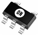
NS5B1G385 Single (NO) Normally Open SPST Analog Switch The NS5B1G385 is Single Pole Single Throw (SPST) high−speed TTL−compatible switch. The low resistance and capacitance characteristics of this switch make it ideal for low−distortion audio, video, and data routing applications. The switch has a normally open http://onsemi.com logic configuration meaning the switch is on (NO connected to COM) MARKING when IN is high. These switches are available in 5−pin SC−70 and DIAGRAMS 5−pin TSOP−5 (SOT23−5) packages for operation over the industrial (−40°C to +85°C) temperature range. SC−70 CG M(cid:2) Features CASE 419A (cid:2) • V Operating Range: 2.0 V to 5.5 V CC • Low On Resistance : R : 4.0 (cid:2) Typical @ V = 4.5 V ON CC • Minimal Propagation Delay : t < 0.5 ns pd 5 • Control Input Compatible with TTL Levels TSOP−5 CD M(cid:2) • ESD Performance: Human Body Model > ±2 kV 5 (SOT23−5) (cid:2) CASE 483 • 1 5−Pin SC−70 or 5−Pin TSOP−5 Packages Available 1 • These are Pb−Free Devices CG = For SC−70 CD = For TSOP−5 Typical Applications M = Date Code • (cid:2) = Pb−Free Package Audio, Video, and High−Speed Data Switching • Mobile Phones (Note: Microdot may be in either location) • Portable Devices • Desktop & Notebook Computing LOGIC DIAGRAM NO COM IN PIN ASSIGNMENTS COM 1 5 VCC NO 2 GND 3 4 IN ORDERING INFORMATION See detailed ordering and shipping information in the package dimensions section on page 4 of this data sheet. © Semiconductor Components Industries, LLC, 2009 1 Publication Order Number: March, 2009 − Rev. 0 NS5B1G385/D
NS5B1G385 PIN DESCRIPTION TRUTH TABLE PIN # Name Direction Description IN Control Input Function 1 COM I/O Common Signal Line L NO Disconnected from COM 2 NO I/O Normally Open Signal Line H NO Connected to COM 3 GND Input Ground 4 IN Input Control Signal Line 5 VCC Input Voltage Supply MAXIMUM RATINGS Symbol Pins Rating Value Condition Unit VCC VCC Positive DC Supply Voltage −0.5 to +7.0 V VIS NO or COM Analog Signal Voltage −0.5 to VCC + 0.5 V VIN IN Control Input Voltage −0.5 to +7.0 V IIS_CON NO or COM Analog Signal Continuous Current (cid:2)300 Closed Switch mA IIS_PK NO or COM Analog Signal Peak Current (cid:2)500 10% Duty Cycle mA IIN IN Control Input Current (cid:2)20 mA TSTG Storage Temperature Range −65 to 150 °C Stresses exceeding Maximum Ratings may damage the device. Maximum Ratings are stress ratings only. Functional operation above the Recommended Operating Conditions is not implied. Extended exposure to stresses above the Recommended Operating Conditions may affect device reliability. RECOMMENDED OPERATING CONDITIONS Symbol Pins Parameter Value Condition Unit VCC VCC Positive DC Supply Voltage 2.0 to 5.5 V VIS NO or COM Analog Signal Voltage GND to VCC V VIN IN Control Input Voltage GND to 5.5 V TA Operating Temperature Range −40 to +85 °C tr, tf Input Rise or Fall Time 20 VCC = 3.3 V ns/V 10 VCC = 5.0 V Minimum and maximum values are guaranteed through test or design across the Recommended Operating Conditions, where applicable. Typical values are listed for guidance only and are based on the particular conditions listed for each section, where applicable. These conditions are valid for all values found in the characteristics tables unless otherwise specified in the test conditions. ESD PROTECTION Pins Description Minimum Voltage All Pins Human Body Model 2 kV http://onsemi.com 2
NS5B1G385 DC ELECTRICAL CHARACTERISTICS CONTROL INPUT (Typical: T = 25°C) −40(cid:2)C to +85(cid:2)C VCC Symbol Pins Parameter Test Conditions (V) Min Typ Max Unit VIH IN Control Input High 4.5 − 5.5 2.0 V VIL IN Control Input Low 4.5 − 5.5 0.8 V IIN IN Control Input Leakage 0 (cid:3) VIN (cid:3) VCC 5.0 ±0.1 ±0.5 (cid:3)A SUPPLY CURRENT AND LEAKAGE (Typical: T = 25°C) −40(cid:2)C to +85(cid:2)C VCC Symbol Pins Parameter Test Conditions (V) Min Typ Max Unit INO NO OFF State Leakage VIN = VIL or VIH 5.5 ±10 ±100 nA (OFF) VNO = 1.0 V VCOM = 4.5 V ICOM COM OFF State Leakage VIN = VIL or VIH 5.5 ±10 ±100 nA (OFF) VNO = 4.5 V VCOM = 1.0 V ICC VCC Quiescent Supply VIN and VIS = VCC or GND 2.0 − 5.5 ±0.1 ±1.0 (cid:3)A ID = 0 A IOFF IN Power Off Leakage VIN = 5.5 V or GND 0 ±0.5 ±1.0 (cid:3)A ON RESISTANCE (Typical: T = 25°C) −40(cid:2)C to +85(cid:2)C VCC Symbol Pins Parameter Test Conditions (V) Min Typ Max Unit RON NO, COM ON Resistance VIS = 0 V, ION = 30 mA 4.5 4.0 7.0 (cid:2) VIS = 0 V, ION = 64 mA 4.5 4.0 7.0 VIS = 2.4 V, ION = 15 mA 4.5 11.5 15 http://onsemi.com 3
NS5B1G385 AC ELECTRICAL CHARACTERISTICS TIMING/FREQUENCY (Typical: T = 25°C, RL = 50 (cid:2), CL = 35 pF, f = 1 MHz) −40(cid:2)C to +85(cid:2)C VCC Symbol Pins Parameter Test Conditions (V) Min Typ Max Unit tON IN to NO Turn On Time As Above, Figures 1 and 2 4.5 6.0 ns tOFF IN to NO Turn Off Time As Above, Figures 1 and 2 4.5 2.0 ns tPD NO to COM Propagation Delay As Above 4.5 0.5 ns BW −3dB Bandwidth CL = 5 pF, Figures 3 and 4 4.5 330 MHz CAPACITANCE (Typical: T = 25°C, RL = 50 (cid:2), CL = 5 pF, f = 1 MHz) −40(cid:2)C to +85(cid:2)C VCC Symbol Pins Parameter Test Conditions (V) Min Typ Max Unit CIN IN Control Input 0 V 2.2 pF CON NO to COM Through Switch VIN = 0V 4.5 V 12 pF COFF NO Unselected Port VIS = 4.5 V, VIN = 4.5 V 4.5 V 4.1 pF DEVICE ORDERING INFORMATION Device Order Number Package Type Tape & Reel Size† NS5B1G385DFT2G SC−70 3000 / Tape & Reel (Pb−Free) NS5B1G385DTT1G TSOP−5 3000 / Tape & Reel (Pb−Free) †For information on tape and reel specifications, including part orientation and tape sizes, please refer to our Tape and Reel Packaging Specifications Brochure, BRD8011/D. http://onsemi.com 4
NS5B1G385 VCC DUT Input 50% 50% VCC Output 0 V 0.1 (cid:3)F VOUT VOH Open 50 (cid:2) 35 pF 90% 90% Output VOL Input tON tOFF Figure 1. t /t ON OFF VCC VCC DUT Input 50% 50% 50 (cid:2) 0 V Output VOUT VOH Open 35 pF Output 10% 10% VOL Input tOFF tON Figure 2. t /t ON OFF 50 (cid:2) DUT Reference Input Transmitted Output 50 (cid:2) Generator 50 (cid:2) Channel switch control/s test socket is normalized. Off isolation is measured across an off channel. On loss is the bandwidth of an On switch. VISO, Bandwidth and VONL are independent of the input signal direction. (cid:4) (cid:5) VOUT VISO = Off Channel Isolation = 20 Log VIN for VIN at 100 kHz (cid:4) (cid:5) VOUT VONL = On Channel Loss = 20 Log VIN for VIN at 100 kHz to 50 MHz Bandwidth (BW) = the frequency 3 dB below VONL VCT = Use VISO setup and test to all other switch analog input/outputs terminated with 50 (cid:2) Figure 3. Off Channel Isolation/On Channel Loss (BW)/Crosstalk (On Channel to Off Channel)/V ONL http://onsemi.com 5
NS5B1G385 0 −10 −20 −1 −30 B) −2 B) −40 d d DE ( DE ( −50 U −3 U T T −60 NI NI G G A −4 A −70 M M −80 −5 −90 −6 −100 10000 1000000 100000000 10000 1000000 100000000 FREQUENCY (Hz) FREQUENCY (Hz) Figure 4. Typical Bandwidth @ V = 5.5 V, Figure 5. Off−Channel Isolation @ V = 5.5 V, CC CC 25(cid:2)C 25(cid:2)C 0.06 0.05 %) 0.04 T ( N 0.03 E C R E P 0.02 0.01 0 10 100 1000 10000 100000 FREQUENCY (Hz) Figure 6. Typical Total Harmonic Distortion @ V = 4.5 V CC http://onsemi.com 6
NS5B1G385 PACKAGE DIMENSIONS SC−70, SOT−353, SC−88A CASE 419A−02 ISSUE J A NOTES: 1. DIMENSIONING AND TOLERANCING G PER ANSI Y14.5M, 1982. 2. CONTROLLING DIMENSION: INCH. 3. 419A−01 OBSOLETE. NEW STANDARD 419A−02. 4. DIMENSIONS A AND B DO NOT INCLUDE 5 4 MOLD FLASH, PROTRUSIONS, OR GATE BURRS. S −B− INCHES MILLIMETERS 1 2 3 DIM MIN MAX MIN MAX A 0.071 0.087 1.80 2.20 B 0.045 0.053 1.15 1.35 C 0.031 0.043 0.80 1.10 D 0.004 0.012 0.10 0.30 D 5 PL 0.2 (0.008) M B M G 0.026 BSC 0.65 BSC H --- 0.004 --- 0.10 J 0.004 0.010 0.10 0.25 N K 0.004 0.012 0.10 0.30 N 0.008 REF 0.20 REF S 0.079 0.087 2.00 2.20 J C K H http://onsemi.com 7
NS5B1G385 PACKAGE DIMENSIONS TSOP−5, SOT23−5 CASE 483−02 ISSUE H NOTES: 1. DIMENSIONING AND TOLERANCING PER NOTE 5 D5X ASME Y14.5M, 1994. 2. CONTROLLING DIMENSION: MILLIMETERS. 0.20 C A B 3. MAXIMUM LEAD THICKNESS INCLUDES 2X 0.10 T LEAD FINISH THICKNESS. MINIMUM LEAD THICKNESS IS THE MINIMUM THICKNESS M OF BASE MATERIAL. 2X 0.20 T 5 4 B S 4. DMIOMLEDN FSLIOANSSH ,A P ARNODT RBU DSOIO NNOST, OINRC GLUATDEE 1 2 3 BURRS. K 5. OPTIONAL CONSTRUCTION: AN L DETAIL Z ADDITIONAL TRIMMED LEAD IS ALLOWED G IN THIS LOCATION. TRIMMED LEAD NOT TO EXTEND MORE THAN 0.2 FROM BODY. A MILLIMETERS DIM MIN MAX DETAIL Z A 3.00 BSC J B 1.50 BSC C C 0.90 1.10 0.05 H SPELAATNIENG GD 0.02.595 BS0C.50 H 0.01 0.10 T J 0.10 0.26 K 0.20 0.60 L 1.25 1.55 M 0 (cid:3) 10 (cid:3) S 2.50 3.00 SOLDERING FOOTPRINT* 1.9 0.074 0.95 0.037 2.4 0.094 1.0 0.039 0.7 (cid:4) (cid:5) 0.028 SCALE 10:1 mm inches *For additional information on our Pb−Free strategy and soldering details, please download the ON Semiconductor Soldering and Mounting Techniques Reference Manual, SOLDERRM/D. ON Semiconductor and are registered trademarks of Semiconductor Components Industries, LLC (SCILLC). SCILLC reserves the right to make changes without further notice to any products herein. SCILLC makes no warranty, representation or guarantee regarding the suitability of its products for any particular purpose, nor does SCILLC assume any liability arising out of the application or use of any product or circuit, and specifically disclaims any and all liability, including without limitation special, consequential or incidental damages. “Typical” parameters which may be provided in SCILLC data sheets and/or specifications can and do vary in different applications and actual performance may vary over time. All operating parameters, including “Typicals” must be validated for each customer application by customer’s technical experts. SCILLC does not convey any license under its patent rights nor the rights of others. SCILLC products are not designed, intended, or authorized for use as components in systems intended for surgical implant into the body, or other applications intended to support or sustain life, or for any other application in which the failure of the SCILLC product could create a situation where personal injury or death may occur. Should Buyer purchase or use SCILLC products for any such unintended or unauthorized application, Buyer shall indemnify and hold SCILLC and its officers, employees, subsidiaries, affiliates, and distributors harmless against all claims, costs, damages, and expenses, and reasonable attorney fees arising out of, directly or indirectly, any claim of personal injury or death associated with such unintended or unauthorized use, even if such claim alleges that SCILLC was negligent regarding the design or manufacture of the part. SCILLC is an Equal Opportunity/Affirmative Action Employer. This literature is subject to all applicable copyright laws and is not for resale in any manner. PUBLICATION ORDERING INFORMATION LITERATURE FULFILLMENT: N. American Technical Support: 800−282−9855 Toll Free ON Semiconductor Website: www.onsemi.com Literature Distribution Center for ON Semiconductor USA/Canada P.O. Box 5163, Denver, Colorado 80217 USA Europe, Middle East and Africa Technical Support: Order Literature: http://www.onsemi.com/orderlit Phone: 303−675−2175 or 800−344−3860 Toll Free USA/Canada Phone: 421 33 790 2910 Fax: 303−675−2176 or 800−344−3867 Toll Free USA/Canada Japan Customer Focus Center For additional information, please contact your local Email: orderlit@onsemi.com Phone: 81−3−5773−3850 Sales Representative http://onsemi.com NS5B1G385/D 8
Mouser Electronics Authorized Distributor Click to View Pricing, Inventory, Delivery & Lifecycle Information: O N Semiconductor: NS5B1G385DFT2G NS5B1G385DTT1G