ICGOO在线商城 > 集成电路(IC) > 接口 - 模拟开关,多路复用器,多路分解器 > ADG1414BRUZ-REEL7
 Datasheet下载
- 型号: ADG1414BRUZ-REEL7
- 制造商: Analog
- 库位|库存: xxxx|xxxx
- 要求:
| 数量阶梯 | 香港交货 | 国内含税 |
| +xxxx | $xxxx | ¥xxxx |
查看当月历史价格
查看今年历史价格
ADG1414BRUZ-REEL7产品简介:
ICGOO电子元器件商城为您提供ADG1414BRUZ-REEL7由Analog设计生产,在icgoo商城现货销售,并且可以通过原厂、代理商等渠道进行代购。 ADG1414BRUZ-REEL7价格参考。AnalogADG1414BRUZ-REEL7封装/规格:接口 - 模拟开关,多路复用器,多路分解器, 8 Circuit IC Switch 1:1 11.5 Ohm 24-TSSOP。您可以下载ADG1414BRUZ-REEL7参考资料、Datasheet数据手册功能说明书,资料中有ADG1414BRUZ-REEL7 详细功能的应用电路图电压和使用方法及教程。
ADG1414BRUZ-REEL7 是由 Analog Devices Inc. 生产的一款模拟开关和多路复用器。它具有低导通电阻(Ron)、低泄漏电流以及高信号带宽等特性,适用于多种需要精确控制信号路径的应用场景。

以下是 ADG1414BRUZ-REEL7 的主要应用场景:

 1. 医疗设备
在医疗设备中,如心电图机(ECG)、超声波设备、病人监护仪等,ADG1414BRUZ-REEL7 可用于选择不同的传感器输入信号,确保信号的准确传输。其低导通电阻和低泄漏电流特性有助于提高测量精度,减少噪声干扰,从而提供更可靠的诊断结果。

 2. 工业自动化
在工业控制系统中,ADG1414BRUZ-REEL7 可用于多路复用传感器信号或执行器控制信号。例如,在数据采集系统中,它可以将多个传感器的信号切换到一个共同的处理通道,简化电路设计并降低成本。此外,其耐高压能力使其适合在恶劣环境下工作,如工厂自动化、过程控制等领域。

 3. 通信设备
在通信设备中,ADG1414BRUZ-REEL7 可用于信号路由和切换,特别是在射频(RF)前端模块中。它的高信号带宽和低插入损耗特性使得它能够在高频信号传输中保持良好的性能,适用于无线通信基站、卫星通信设备等。

 4. 音频处理
在音频处理设备中,ADG1414BRUZ-REEL7 可用于多路音频信号的选择和切换。例如,在混音器或多声道音频系统中,它可以灵活地选择不同的音频输入源,并将其传输到相应的输出通道。其低失真特性有助于保持音频信号的高质量。

 5. 测试与测量仪器
在测试与测量仪器中,如示波器、信号发生器等,ADG1414BRUZ-REEL7 可用于多路信号的快速切换,确保测试过程中信号的稳定性和准确性。其快速响应时间和低延迟特性使得它特别适合高速测试应用。

总之,ADG1414BRUZ-REEL7 凭借其优异的电气特性和可靠性,广泛应用于对信号完整性要求较高的领域,帮助工程师实现高效、精确的信号切换和处理。
| 参数 | 数值 |
| 产品目录 | 集成电路 (IC)半导体 |
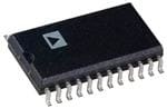
| 描述 | IC SW SPST 9.5OHM RON 24TSSOP模拟开关 IC iCMOS Serially-Cntrl Octal SPST |
| DevelopmentKit | EVAL-CN0209-SDPZ |
| 产品分类 | |
| 品牌 | Analog Devices |
| 产品手册 | |
| 产品图片 |
|
| rohs | 符合RoHS无铅 / 符合限制有害物质指令(RoHS)规范要求 |
| 产品系列 | 开关 IC,模拟开关 IC,Analog Devices ADG1414BRUZ-REEL7iCMOS® |
| 数据手册 | |
| 产品型号 | ADG1414BRUZ-REEL7 |
| 产品种类 | 模拟开关 IC |
| 供应商器件封装 | 24-TSSOP |
| 其它名称 | ADG1414BRUZ-REEL7DKR |
| 功能 | |
| 包装 | Digi-Reel® |
| 商标 | Analog Devices |
| 安装类型 | 表面贴装 |
| 安装风格 | SMD/SMT |
| 导通电阻 | 21.5 欧姆 |
| 封装 | Reel |
| 封装/外壳 | 24-TSSOP(0.173",4.40mm 宽) |
| 封装/箱体 | TSSOP-24 |
| 工作温度 | -40°C ~ 125°C |
| 工作电源电压 | 16.5 V |
| 工厂包装数量 | 1000 |
| 开关数量 | 8 |
| 开关电压—最大值 | 16.5 V |
| 开关电流—最大值 | 300 mA |
| 开关配置 | SPST |
| 最大功率耗散 | 2.8 mW |
| 最大工作温度 | + 125 C |
| 最小工作温度 | - 40 C |
| 标准包装 | 1 |
| 电压-电源,单/双 (±) | 4.5 V ~ 16.5 V, ±2.25 V ~ 8.25 V |
| 电压源 | 单/双电源 |
| 电流-电源 | 1nA |
| 电源电压-最大 | 16.5 V |
| 电源电压-最小 | 16.5 V |
| 电源电流—最大值 | 1 uA |
| 电路 | 8 x SPST - NO |
| 空闲时间—最大值 | 25 ns |
| 系列 | ADG1414 |
| 运行时间—最大值 | 75 ns |


- 商务部:美国ITC正式对集成电路等产品启动337调查
- 曝三星4nm工艺存在良率问题 高通将骁龙8 Gen1或转产台积电
- 太阳诱电将投资9.5亿元在常州建新厂生产MLCC 预计2023年完工
- 英特尔发布欧洲新工厂建设计划 深化IDM 2.0 战略
- 台积电先进制程称霸业界 有大客户加持明年业绩稳了
- 达到5530亿美元!SIA预计今年全球半导体销售额将创下新高
- 英特尔拟将自动驾驶子公司Mobileye上市 估值或超500亿美元
- 三星加码芯片和SET,合并消费电子和移动部门,撤换高东真等 CEO
- 三星电子宣布重大人事变动 还合并消费电子和移动部门
- 海关总署:前11个月进口集成电路产品价值2.52万亿元 增长14.8%


PDF Datasheet 数据手册内容提取
9.5 Ω R , ±15 V/+12 V/±5 V iCMOS, ON Serially-Controlled Octal SPST Switches Data Sheet ADG1414 FEATURES FUNCTIONAL BLOCK DIAGRAM SPI interface ADG1414 Supports daisy-chain mode S1 D1 9.5 Ω on resistance at 25°C and ±15 V dual supply S2 D2 1.6 Ω on-resistance flatness at 25°C and ±15 V dual supply S3 D3 Fully specified at ±15 V, +12 V, ±5 V S4 D4 S5 D5 3 V logic-compatible inputs S6 D6 Rail-to-rail operation S7 D7 24-lead TSSOP and 24-lead, 4 mm × 4 mm LFCSP S8 D8 APPLICATIONS INPUT SHIFT SDO REGISTER Automatic test equipment DBaatttae arycq-puoiswiteiroend s syysstteemmss SCLK DIN SYNC RESET/VL 08497-001 Sample-and-hold systems Figure 1. Audio signal routing Video signal routing Communication systems GENERAL DESCRIPTION The ADG1414 is a monolithic complementary metal-oxide The ADG1414 uses a versatile 3-wire serial interface that semiconductor (CMOS) device containing eight independently operates at clock rates of up to 50 MHz and is compatible with selectable switches designed on an industrial CMOS (iCMOS®) standard SPI, QSPI™, MICROWIRE™, and DSP interface process. iCMOS is a modular manufacturing process combining standards. The output of the shift register, SDO, enables a high voltage CMOS and bipolar technologies. iCMOS components number of these devices to be daisy chained. can tolerate high supply voltages while providing increased perfor- At power-up, all switches are in the off condition, and the mance, dramatically lower power consumption, and reduce the internal registers contain all zeros. package size. PRODUCT HIGHLIGHTS The ADG1414 is a set of octal, single-pole, single-throw (SPST) switches controlled via a 3-wire serial interface. On resistance is 1. 50 MHz serial interface. matched closely between switches and is very flat over the full 2. 9.5 Ω on resistance. signal range. Each switch conducts equally well in both directions 3. 1.6 Ω on-resistance flatness. and the input signal range extends to the supplies. 4. 24-lead TSSOP and 4 mm × 4 mm LFCSP packages. Data is written to these devices in the form of eight bits; each bit corresponds to one channel. Rev. B Document Feedback Information furnished by Analog Devices is believed to be accurate and reliable. However, no responsibility is assumed by Analog Devices for its use, nor for any infringements of patents or other One Technology Way, P.O. Box 9106, Norwood, MA 02062-9106, U.S.A. rights of third parties that may result from its use. Specifications subject to change without notice. No license is granted by implication or otherwise under any patent or patent rights of Analog Devices. Tel: 781.329.4700 ©2009–2015 Analog Devices, Inc. All rights reserved. Trademarks and registered trademarks are the property of their respective owners. Technical Support www.analog.com
ADG1414 Data Sheet TABLE OF CONTENTS Features .............................................................................................. 1 ESD Caution...................................................................................9 Applications ....................................................................................... 1 Pin Configurations and Function Descriptions ......................... 10 Functional Block Diagram .............................................................. 1 Typical Performance Characteristics ........................................... 12 Product Highlights ........................................................................... 1 Test Circuits ..................................................................................... 15 Revision History ............................................................................... 2 Terminology .................................................................................... 17 Specifications ..................................................................................... 3 Theory of Operation ...................................................................... 18 ±15 V Dual Supply ....................................................................... 3 Serial Interface ............................................................................ 18 12 V Single Supply ........................................................................ 4 Input Shift Register .................................................................... 18 ±5 V Dual Supply ......................................................................... 6 Power-On Reset .......................................................................... 18 Continuous Current per Channel .............................................. 7 Daisy Chaining ........................................................................... 18 Timing Characteristics ................................................................ 8 Outline Dimensions ....................................................................... 19 Absolute Maximum Ratings ............................................................ 9 Ordering Guide .......................................................................... 19 Thermal Resistance ...................................................................... 9 REVISION HISTORY 11/15—Rev. A to Rev. B Changes to V /V Parameter, Table 2 ......................................... 5 DD SS Updated Outline Dimensions ....................................................... 19 1/13—Rev. 0 to Rev. A Changes to RESET/V Pin Description Column, Table 9 ......... 11 L Changes to Power-On Reset Section ............................................ 19 Updated Outline Dimensions ....................................................... 20 10/09—Revision 0: Initial Version Rev. B | Page 2 of 19
Data Sheet ADG1414 SPECIFICATIONS ±15 V DUAL SUPPLY V = 15 V ± 10%, V = −15 V ± 10%, V = 2.7 V to 5.5 V, GND = 0 V, unless otherwise noted. DD SS L Table 1. −40°C to −40°C to Parameter +25°C +85°C +125°C Unit Test Conditions/Comments ANALOG SWITCH Analog Signal Range V to V V SS DD On Resistance (R ) 9.5 Ω typ V = +13.5 V, V = −13.5 V, V = ±10 V, ON DD SS S I = −10 mA; see Figure 23 S 11.5 14 16 Ω max On-Resistance Match Between Channels (ΔR ) 0.55 Ω typ V = +13.5 V, V = −13.5 V, V = ±10 V, ON DD SS S I = −10 mA S 1 1.5 1.7 Ω max On-Resistance Flatness (R ) 1.6 Ω typ V = +13.5 V, V = −13.5 V, V = ±10 V, FLAT (ON) DD SS S I = −10 mA S 1.9 2.15 2.3 Ω max LEAKAGE CURRENTS V = +16.5 V, V = −16.5 V DD SS Source Off Leakage, IS (Off) ±0.05 nA typ VS = ±10 V, VD = ∓10 V; see Figure 24 ±0.15 ±1 ±2 nA max Drain Off Leakage, ID (Off) ±0.05 nA typ VS = ±10 V, VD = ∓10 V; see Figure 24 ±0.15 ±1 ±2 nA max Channel On Leakage, I , I (On) ±0.1 nA typ V = V = ±10 V; see Figure 25 D S S D ±0.3 ±2 ±4 nA max DIGITAL INPUTS Input High Voltage (V ) 2.0 V min INH Input Low Voltage (V ) 0.8 V max INL Input Current ±0.001 µA typ V = V or V IN GND L ±0.1 µA max Digital Input Capacitance (C ) 4 pF typ IN LOGIC OUTPUTS (SDO) Output Low Voltage (V )1 0.4 V max I = 3 mA OL SINK 0.6 V max I = 6 mA SINK High Impedance Leakage Current 0.001 µA typ ±1 µA max High Impedance Output Capacitance1 4 pF typ DYNAMIC CHARACTERISTICS1 t 75 ns typ R = 100 Ω, C = 35 pF ON L L 93 110 120 ns max V = 10 V; see Figure 30 S t 25 ns typ R = 100 Ω, C = 35 pF OFF L L 35 35 35 ns max V = 10 V; see Figure 30 S Charge Injection 10 pC typ V = 0 V, R = 0 Ω, C = 1 nF; see Figure 31 S S L Off Isolation −73 dB typ R = 50 Ω, C = 5 pF, f = 1 MHz; see Figure 26 L L Channel-to-Channel Crosstalk −75 dB typ R = 50 Ω, C = 5 pF, f = 1 MHz; see Figure 27 L L Total Harmonic Distortion (THD + N) 0.05 % typ R = 110 Ω, 15 V p-p, f = 20 Hz to 20 kHz; L see Figure 29 −3 dB Bandwidth 256 MHz typ R = 50 Ω, C = 5 pF; see Figure 28 L L Insertion Loss 0.55 dB typ R = 50 Ω, C = 5 pF, f = 1 MHz; see Figure 28 L L C , C (Off) 8 pF typ f = 1 MHz D S C , C (On) 32 pF typ f = 1 MHz D S Rev. B | Page 3 of 19
ADG1414 Data Sheet −40°C to −40°C to Parameter +25°C +85°C +125°C Unit Test Conditions/Comments POWER REQUIREMENTS V = +16.5 V, V = −16.5 V DD SS I 0.001 µA typ Digital inputs = 0 V or V DD L 1 µA max I Inactive 0.3 µA typ Digital inputs = 0 V or V L L 1 µA max I Active at 30 MHz 0.26 mA typ Digital inputs toggle between 0 V and V L L 0.3 0.35 mA max I Active at 50 MHz 0.42 mA typ Digital inputs toggle between 0 V and V L L 0.5 0.55 mA max I 0.001 µA typ Digital inputs = 0 V or V SS L 1 µA max V /V ±4.5/±16.5 V min/max DD SS 1 Guaranteed by design, not subject to production test. 12 V SINGLE SUPPLY V = 12 V ± 10%, V = 0 V, V = 2.7 V to 5.5 V, GND = 0 V, unless otherwise noted. DD SS L Table 2. −40°C to −40°C to Parameter +25°C +85°C +125°C Unit Test Conditions/Comments ANALOG SWITCH Analog Signal Range 0 to V V DD On Resistance (R ) 18 Ω typ V = 10.8 V, V = 0 V; V = 0 V to 10 V, ON DD SS S I = −10 mA; see Figure 23 S 21.5 26 28.5 Ω max On-Resistance Match Between Channels (ΔR ) 0.55 Ω typ V = 10.8 V, V = 0 V; V = 0 V to 10 V, ON DD SS S I = −10 mA S 1.2 1.6 1.8 Ω max On-Resistance Flatness (R ) 5 Ω typ V = 10.8 V, V = 0 V; V = 0 V to 10 V, FLAT (ON) DD SS S I = −10 mA S 6 6.9 7.3 Ω max LEAKAGE CURRENTS V = 10.8 V DD Source Off Leakage, I (Off) ±0.02 nA typ V = 1 V/10 V, V = 10 V/1 V; see Figure 24 S S D ±0.15 ±1 ±2 nA max Drain Off Leakage, I (Off) ±0.02 nA typ V = 1 V/10 V, V = 10 V/1 V; see Figure 24 D S D ±0.15 ±1 ±2 nA max Channel On Leakage, I , I (On) ±0.05 nA typ V = V = 1 V or 10 V; see Figure 25 D S S D ±0.3 ±2 ±4 nA max DIGITAL INPUTS Input High Voltage (V ) 2.0 V min INH Input Low Voltage (V ) 0.8 V max INL Input Current ±0.001 µA typ V = V or V IN GND L ±0.1 µA max Digital Input Capacitance (C ) 4 pF typ IN LOGIC OUTPUTS (SDO) Output Low Voltage (V )1 0.4 V max I = 3 mA OL SINK 0.6 V max I = 6 mA SINK High Impedance Leakage Current ±1 µA max High Impedance Output Capacitance1 4 pF typ Rev. B | Page 4 of 19
Data Sheet ADG1414 −40°C to −40°C to Parameter +25°C +85°C +125°C Unit Test Conditions/Comments DYNAMIC CHARACTERISTICS1 t 145 ns typ R = 100 Ω, C = 35 pF ON L L 185 220 240 ns max V = 8 V; see Figure 30 S t 35 ns typ R = 100 Ω, C = 35 pF OFF L L 45 46 46 ns max V = 8 V; see Figure 30 S Charge Injection 8 pC typ V = 6 V, R = 0 Ω, C = 1 nF; see Figure 31 S S L Off Isolation −70 dB typ R = 50 Ω, C = 5 pF, f = 1 MHz; L L see Figure 26 Channel-to-Channel Crosstalk −75 dB typ R = 50 Ω, C = 5 pF, f = 1 MHz; L L see Figure 27 −3 dB Bandwidth 240 MHz typ R = 50 Ω, C = 5 pF; see Figure 28 L L Insertion Loss 1.15 dB typ R = 50 Ω, C = 5 pF, f = 1 MHz; L L see Figure 28 C , C (Off) 12 pF typ f = 1 MHz D S C , C (On) 33 pF typ f = 1 MHz D S POWER REQUIREMENTS V = +13.2 V DD I 0.001 µA typ Digital inputs = 0 V or V DD L 1 µA max I Inactive 0.3 µA typ Digital inputs = 0 V or V L L 1 µA max I Active at 30 MHz 0.26 mA typ Digital inputs toggle between 0 V and V L L 0.3 0.35 mA max I Active at 50 MHz 0.42 mA typ Digital inputs toggle between 0 V and V L L 0.5 0.55 mA max I 0.001 µA typ Digital inputs = 0 V or V SS L 1 µA max V /V 5/16.5 V min/max DD SS 1 Guaranteed by design, not subject to production test. Rev. B | Page 5 of 19
ADG1414 Data Sheet ±5 V DUAL SUPPLY V = +5 V ± 10%, V = −5 V ± 10%, V = 2.7 V to V , GND = 0 V, unless otherwise noted. DD SS L DD Table 3. −40°C to −40°C to Parameter +25°C +85°C +125°C Unit Test Conditions/Comments ANALOG SWITCH Analog Signal Range V to V V SS DD On Resistance (R ) 21 Ω typ V = +4.5 V, V = −4.5 V, V = ±4.5 V, ON DD SS S I = −10 mA; see Figure 23 S 25 29 32 Ω max On-Resistance Match Between Channels (ΔR ) 0.6 Ω typ V = +4.5 V, V = −4.5 V, V = ±4.5V, ON DD SS S I = −10 mA S 1.3 1.7 1.9 Ω max On-Resistance Flatness (R ) 5.2 Ω typ V = +4.5 V, V = −4.5 V, V = ±4.5 V; FLAT (ON) DD SS S 6.4 7.3 7.6 Ω max I = −10 mA S LEAKAGE CURRENTS V = +5.5 V, V = −5.5 V DD SS Source Off Leakage, IS (Off) ±0.02 nA typ VS = ±4.5 V, VD = ∓4.5 V; see Figure 24 ±0.15 ±1 ±2 nA max Drain Off Leakage, ID (Off) ±0.02 nA typ VS = ±4.5 V, VD = ∓4.5 V; see Figure 24 ±0.15 ±1 ±2 nA max Channel On Leakage, I , I (On) ±0.05 nA typ V = V = ±4.5 V; see Figure 25 D S S D ±0.3 ±2 ±4 nA max DIGITAL INPUTS Input High Voltage (V ) 2.0 V min INH Input Low Voltage (V ) 0.8 V max INL Input Current ±0.001 µA typ V = V or V IN GND L ±0.1 µA max Digital Input Capacitance (C ) 4 pF typ IN LOGIC OUTPUTS (SDO) Output Low Voltage (V )1 0.4 V max I = 3 mA OL SINK 0.6 V max I = 6 mA SINK High Impedance Leakage Current ±1 µA max High Impedance Output Capacitance1 4 pF typ DYNAMIC CHARACTERISTICS1 t 190 ns typ R = 100 Ω, C = 35 pF ON L L 250 290 320 ns max V = 3 V; see Figure 30 S t 45 ns typ R = 100 Ω, C = 35 pF OFF L L 60 65 70 ns max V = 3 V; see Figure 30 S Charge Injection 7 pC typ V = 0 V, R = 0 Ω, C = 1 nF; see Figure 31 S S L Off Isolation –70 dB typ R = 50 Ω, C = 5 pF, f = 1 MHz; see Figure 26 L L Channel-to-Channel Crosstalk –75 dB typ R = 50 Ω, C = 5 pF, f = 1 MHz; see Figure 27 L L Total Harmonic Distortion (THD + N) 0.14 % typ R = 110 Ω, 5 V p-p, f = 20 Hz to 20 kHz; L see Figure 29 −3 dB Bandwidth 256 MHz typ R = 50 Ω, C = 5 pF; see Figure 28 L L Insertion Loss 1 dB typ R = 50 Ω, C = 5 pF, f = 1 MHz; see Figure 28 L L C , C (Off) 11 pF typ f = 1 MHz D S C , C (On) 35 pF typ f = 1 MHz D S Rev. B | Page 6 of 19
Data Sheet ADG1414 −40°C to −40°C to Parameter +25°C +85°C +125°C Unit Test Conditions/Comments POWER REQUIREMENTS V = +5.5 V, V = −5.5 V DD SS I 0.001 µA typ Digital inputs = 0 V or V DD L 1 µA max I Inactive 0.3 µA typ Digital inputs = 0 V or V L L 1 µA max I Active at 30 MHz 0.26 mA typ Digital inputs toggle between 0 V and V L L 0.3 0.35 mA max I Active at 50 MHz 0.42 mA typ Digital inputs toggle between 0 V and V L L 0.5 0.55 mA max I 0.001 µA typ Digital inputs = 0 V or V SS L 1 µA max V /V ±4.5/±16.5 V min/max DD SS 1 Guaranteed by design, not subject to production test. CONTINUOUS CURRENT PER CHANNEL Guaranteed by design, not subject to production test. Table 4. Eight Channels On Parameter 25°C 85°C 125°C Unit Test Conditions/Comments CONTINUOUS CURRENT PER CHANNEL ±15 V Dual Supply V = +13.5 V, V = −13.5 V DD SS 24-Lead TSSOP (θ = 112.6°C/W) 67 46 31 mA max JA 24-Lead LFCSP (θ = 30.4°C/W) 121 75 42 mA max JA 12 V Single Supply V = 10.8 V, V = 0 V DD SS 24-Lead TSSOP (θ = 112.6°C/W) 64 44 30 mA max JA 24-Lead LFCSP (θ = 30.4°C/W) 115 72 41 mA max JA ±5 V Dual Supply V = +4.5 V, V = −4.5 V DD SS 24-Lead TSSOP (θ = 112.6°C/W) 48 35 22 mA max JA 24-Lead LFCSP (θ = 30.4°C/W) 86 57 36 mA max JA Guaranteed by design and characterization, not production tested. Table 5. One Channel On Parameter 25°C 85°C 125°C Unit Test Conditions/Comments CONTINUOUS CURRENT PER CHANNEL ±15 V Dual Supply V = +13.5 V, V = −13.5 V DD SS 24-Lead TSSOP (θ = 112.6°C/W) 169 97 48 mA max JA 24-Lead LFCSP (θ = 30.4°C/W) 295 139 55 mA max JA 12 V Single Supply V = 10.8 V, V = 0 V DD SS 24-Lead TSSOP (θ = 112.6°C/W) 161 93 47 mA max JA 24-Lead LFCSP (θ = 30.4°C/W) 281 135 54 mA max JA ±5 V Dual Supply V = +4.5 V, V = −4.5 V DD SS 24-Lead TSSOP (θ = 112.6°C/W) 122 76 43 mA max JA 24-Lead LFCSP (θ = 30.4°C/W) 214 114 51 mA max JA Rev. B | Page 7 of 19
ADG1414 Data Sheet TIMING CHARACTERISTICS All input signals are specified with t = t = 1 ns/V (10% to 90% of V ) and timed from a voltage level of (V + V )/2 (see Figure 2). R F DD IL IH V = 4.5 V to 16.5 V; V = −16.5 V to 0 V; V = 2.7 V to 5.5 V or V (whichever is less); GND = 0 V; all specifications T to T , DD SS L DD MIN MAX unless otherwise noted. Guaranteed by design and characterization, not production tested. Table 6. Parameter Limit at T , T Unit Conditions/Comments MIN MAX t1 20 ns min SCLK cycle time 1 t 9 ns min SCLK high time 2 t 9 ns min SCLK low time 3 t 5 ns min SYNC to SCLK active edge setup time 4 t 5 ns min Data setup time 5 t 5 ns min Data hold time 6 t 5 ns min SCLK active edge to SYNC rising edge 7 t 15 ns min Minimum SYNC high time 8 t 5 ns min SYNC rising edge to next SCLK active edge ignored 9 t 5 ns min SCLK active edge to SYNC falling edge ignored 10 t 2 40 ns max SCLK rising edge to SDO valid 11 t 15 ns min Minimum RESET pulse width 12 1 Maximum SCLK frequency is 50 MHz at VDD = 4.5 V to 16.5 V; VSS = −16.5 V to 0 V, VL = 2.7 V to 5.5 V or VDD (whichever is less); GND = 0 V. 2 Measured with the 1 kΩ pull-up resistor to VL and 20 pF load. t11 determines the maximum SCLK frequency in daisy-chain mode. Timing Diagrams t10 t1 t 9 SCLK t8 t3 t2 t7 t 4 SYNC t 6 t 5 DIN DB7 DB0 RESET t12 08497-002 Figure 2. Serial Write Operation t 1 SCLK 8 16 t8 t4 t3 t2 t7 t9 SYNC t 5 t 6 DIN DB7 DB0 DB7 DB0 INPUT WORD FOR DEVICE N INPUT WORD FOR DEVICE N + 1 t 11 SDO DB31 DB0 UNDEFINED INPUT WORD FOR DEVICE N 08497-003 Figure 3. Daisy-Chain Timing Diagram Rev. B | Page 8 of 19
Data Sheet ADG1414 ABSOLUTE MAXIMUM RATINGS T = 25°C, unless otherwise noted. Stresses at or above those listed under Absolute Maximum A Ratings may cause permanent damage to the product. This is a Table 7. stress rating only; functional operation of the product at these Parameter Rating or any other conditions above those indicated in the operational V to V 35 V DD SS section of this specification is not implied. Operation beyond V to GND −0.3 V to +25 V DD the maximum operating conditions for extended periods may V to GND +0.3 V to −25 V SS affect product reliability. V to GND −0.3 V to +7 V L Only one absolute maximum rating may be applied at any one Analog Inputs1 V − 0.3 V to V + 0.3 V or SS DD 30 mA, whichever occurs first time. Digital Inputs1 GND − 0.3 V to V + 0.3 V or THERMAL RESISTANCE L 30 mA, whichever occurs first Continuous Current, Sx or Dx Pins Table 4 specifications + 15% Table 8. Thermal Resistance Peak Current, Sx or Dx (Pulsed at Package Type θJA θJC Unit 1 ms, 10% Duty Cycle Maximum) 24-Lead TSSOP1 112.6 50 °C/W TSSOP Package 300 mA 24-Lead LFCSP2 30.4 °C/W LFCSP Package 400 mA 1 4-layer board. Operating Temperature Range 2 4-layer board and exposed paddle soldered to VSS. Industrial (B Version) –40°C to +125°C ESD CAUTION Storage Temperature Range −65°C to +150°C Junction Temperature 150°C Reflow Soldering Peak 260°C Temperature, Pb free Time at Peak Temperature 10 sec to 40 sec 1 Overvoltages at the analog and digital inputs are clamped by internal diodes. Limit the current to the maximum ratings given. Rev. B | Page 9 of 19
ADG1414 Data Sheet PIN CONFIGURATIONS AND FUNCTION DESCRIPTIONS SCLK 1 24 SYNC V/TL K C E VDD 2 23 RESET/VL NID VDDLCS NYS SER ODS DIN 3 22 SDO 42 32 22 12 02 91 GND 4 21 VSS S1 5 20 S8 GND1 18 VSS ADG1414 S12 17 S8 D1 6 TOP VIEW 19 D8 D13 ADG1414 16 D8 S2 7 (Not to Scale) 18 S7 S24 TOP VIEW 15 S7 (Not to Scale) D2 8 17 D7 D25 14 D7 S36 13 S6 S3 9 16 S6 D3 10 15 D6 7 8 9 01 11 21 S4 11 14 S5 3D 4S 4D 5D 5S 6D D4 12 13 D5 08497-004 N1.O ETXEPSOSED PAD TIED TO SUBSTRATE, VSS.08497-005 Figure 4. TSSOP Pin Configuration Figure 5. LFCSP Pin Configuration Table 9. Pin Function Descriptions Pin No. TSSOP LFCSP Mnemonic Description 1 22 SCLK Serial Clock Input. Data is clocked into the input shift register on the falling edge of the serial clock input. Data can be transferred at rates of up to 50 MHz. 2 23 V Most Positive Power Supply Potential. DD 3 24 DIN Serial Data Input. This device has an 8-bit shift register. Data is clocked into the register on the falling edge of the serial clock input. 4 1 GND Ground (0 V) Reference. 5 2 S1 Source Terminal 1. This pin can be an input or an output. 6 3 D1 Drain Terminal 1. This pin can be an input or an output. 7 4 S2 Source Terminal 2. This pin can be an input or an output. 8 5 D2 Drain Terminal 2. This pin can be an input or an output. 9 6 S3 Source Terminal 3. This pin can be an input or an output. 10 7 D3 Drain Terminal 3. This pin can be an input or an output. 11 8 S4 Source Terminal 4. This pin can be an input or an output. 12 9 D4 Drain Terminal 4. This pin can be an input or an output. 13 10 D5 Drain Terminal 5. This pin can be an input or an output. 14 11 S5 Source Terminal 5. This pin can be an input or an output. 15 12 D6 Drain Terminal 6. This pin can be an input or an output. 16 13 S6 Source Terminal 6. This pin can be an input or an output. 17 14 D7 Drain Terminal 7. This pin can be an input or an output. 18 15 S7 Source Terminal 7. This pin can be an input or an output. 19 16 D8 Drain Terminal 8. This pin can be an input or an output. 20 17 S8 Source Terminal 8. This pin can be an input or an output. 21 18 V Most Negative Power Supply Potential. In single-supply applications, it can be connected to SS ground. 22 19 SDO Serial Data Output. This pin can be used for daisy-chaining a number of these devices together or for reading back the data in the shift register for diagnostic purposes. The serial data is transferred on the rising edge of SCLK and is valid on the falling edge of the clock. Pull this open-drain output to the supply with an external resistor. 23 20 RESET/V RESET/Logic Power Supply Input (V). Under normal operation, drive the RESET/V pin with a 2.7 V L L L to 5 V supply. Pull the pin low (<0.8 V) for a short period of time (15 ns is sufficient) to complete a hardware reset. All switches are opened, and the appropriate registers are cleared to 0. When using the RESET/V pin to complete a hardware reset, all other SPI pins (SYNC, SCLK, and DIN) L must be driven low. Rev. B | Page 10 of 19
Data Sheet ADG1414 Pin No. TSSOP LFCSP Mnemonic Description 24 21 SYNC Active Low Control Input. This is the frame synchronization signal for the input data. When SYNC goes low, it powers on the SCLK and DIN buffers and enables the input shift register. Data is transferred in on the falling edges of the following clocks. Taking SYNC high updates the switch condition. N/A1 EP Exposed Pad Exposed Pad. Exposed pad tied to the substrate, V . SS 1 N/A means not applicable. Rev. B | Page 11 of 19
ADG1414 Data Sheet TYPICAL PERFORMANCE CHARACTERISTICS 16 18 14 VVDSSD == –+1100VV VVDSSD == –+1133..55VV 15 12 VDD = +12V CE (Ω) 10 VSS = –12V CE (Ω) 12 TA = +125°C N N A A ST 8 ST 9 TA = +85°C SI SI ON RE 64 VVDSSD == –+1155VV VVDSSD == –+1166..55VV ON RE 6 TTAA == +–4205°°CC 3 2 TISA = = – 2150°mCA VVDSSD == –+1155VV –016.5–13.5–10.5 –7.5 –4.5 –V1S.,5 VD1 (.V5) 4.5 7.5 10.5 13.5 16.5 08497-006 0–15 –10 –5 VS, V0D (V) 5 10 15 08497-009 Figure 6. On Resistance as a Function of VD (VS), Dual Supply Figure 9. On Resistance as a Function of VD (VS), for Different Temperatures, (VDD = 10 V to 16.5 V and VSS = −10 V to −16.5 V) ±15 V Dual Supply 35 30 VDD = +3.0V VSS = –3.0V 30 25 VDD = +4.5V CE (Ω) 25 VSS = –4.5V VDD = +5.0V CE (Ω) 20 TA = +125°C AN 20 VSS = –5.0V AN TA = +85°C ST ST 15 ESI 15 ESI TA = +25°C R R ON 10 VDD = +5.5V ON 10 TA = –40°C VSS = –5.5V VDD = +7V 5 VSS = –7V 5 ITSA = = – 2150°mCA VVDSSD == –+55VV 0–7 –5 –3 –1VS, VD (V1) 3 5 7 08497-007 0–5 –4 –3 –2 –1VS, V0D (V)1 2 3 4 5 08497-010 Figure 7. On Resistance as a Function of VD (Vs), Dual Supply Figure 10. On Resistance as a Function of VD (VS), for Different Temperatures, (VDD = 3.0 V to 7 V and VSS = −3.0 V to −7 V) ±5 V Dual Supply 40 25 35 VDD = +5V VSS = 0V 20 30 E (Ω) 25 VVDSSD == 0+V8V E (Ω) TA = +125°C C C 15 N N SISTA 20 VDD = +10.8V VVDSSD == 0+V12V SISTA TA = +85°C N RE 15 VSS = 0V N RE 10 TA = +25°C O O TA = –40°C 10 5 5 TISA = = – 2150°mCA VVDSSD == 0+V15V VVDSSD == 0+V13.2V VVDSSD == 0+V12V 00 1.5 3.0 4.5 6.0VS, 7V.D5 (V)9.0 10.5 12.0 13.5 15.0 08497-008 00 2 4 VS, V6D (V) 8 10 12 08497-011 Figure 8. On Resistance as a Function of VD (VS), Single Supply Figure 11. On Resistance as a Function of VD (VS), for Different Temperatures, 12 V Single Supply Rev. B | Page 12 of 19
Data Sheet ADG1414 2.5 500 VDD = +15V IDD PER LOGIC INPUT 2.0 VSS = –15V VL = 5.5V TA = 25°C VBIAS = +10/–10V ID, IS (ON) – – 400 A) 1.5 ID (OFF) –+ n T ( 1.0 IS (OFF) +– N CURRE 0.5 ID, IS (ON) ++ (µA)D 300 GE 0 ID 200 A AK –0.5 E L IS (OFF) –+ –1.0 100 ID (OFF) +– –1.5 VL = 2.7V –2.00 20 40TEMPER6A0TURE (°8C0) 100 120 08497-013 00 0.5 1.0 1.5 L2O.0GIC 2L.E5VEL3 .(0V) 3.5 4.0 4.5 5.0 08497-016 Figure 12. Leakage Current as a Function of Temperature, ±15 V Dual Supply Figure 15. IDD vs. Logic Level 3.0 80 VDD = +5V TA = 25°C 2.5 VVSBSIA =S –=5 +V4.5/–4.5V ID, IS (ON) ++ 60 nA) 2.0 pC) 40 T ( N ( N 1.5 O GE CURRE 1.0 ID (OFF) –I+D, IS (ON) – – E INJECTI 200 VVSDSD == –+55VV VVDSSD == 0+V12V A 0.5 G LEAK 0 IS (OFF) +– CHAR –20 VVDSSD == –+1155VV –0.5 IS (OFF) –+ –40 ID (OFF) +– –1.00 20 40TEMPER6A0TURE (°8C0) 100 120 08497-014 –60–15 –10 –5 VS0 (V) 5 10 15 08497-017 Figure 13. Leakage Current as a Function of Temperature, Figure 16. Charge Injection vs. Source Voltage (VS) ±5 V Dual Supply 3.0 300 VDD = 12V 2.5 VVSBSIA =S 0=V 1V/10V ID, IS (ON) ++ 250 nA) 2.0 tON (±5V) T ( 200 CURREN 11..05 ID (OFIDF,) I S– +(ON) – – ME (ns) 150 tON (+12V) AGE 0.5 IS (OFF) +– TI EAK 100 tON (±15V) L 0 tOFF (±5V) 50 –0.5 IS (OFF) –+ ID (OFF) +– tOFF (±15V) tOFF (+12V) –1.00 20 40TEMPER6A0TURE (°8C0) 100 120 08497-015 0–40 –20 0 T2E0MPER4A0TURE6 0(°C) 80 100 120 08497-018 Figure 14. Leakage Current as a Function of Temperature, 12 V Single Supply Figure 17. Transition Time vs. Temperature Rev. B | Page 13 of 19
ADG1414 Data Sheet 0 0.20 TA = 25°C LOAD = 110Ω VDD = +15V 0.18 TA = 25°C –20 VSS = –15V 0.16 VDD = +5V, VSS = –5V, VS = +5V p-p dB) –40 0.14 TION ( N (%) 0.12 OLA –60 D + 0.10 FF IS –80 TH 0.08 VDD = +15V, VSS = –15V, VS = +10V p-p O 0.06 0.04 –100 0.02 –120 0 1k 10k 100kFREQUE1MNCY (Hz)10M 100M 1G 08497-019 0 5000 FREQ1U0E,0N0C0Y (Hz) 15,000 20,000 08497-023 Figure 18. Off Isolation vs. Frequency Figure 21. THD + N vs. Frequency, ±15 V Dual Supply 0 0 TA = 25°C TA = 25°C VDD = +15V VDD = +15V –0.5 VSS = –15V –20 VSS = –15V –1.0 B) d –40 N LOSS ( ––21..05 RR (dB) –60 NOC ADPEACCOIUTOPLRISNG O S ERTI –2.5 ACP DECOUPLING NS –80 CAPACITORS I –3.0 –100 –3.5 –4.0 –120 1k 10k 100kFREQUE1MNCY (Hz)10M 100M 1G 08497-012 1k 10k FREQU1E0N0kCY (Hz) 1M 10M 08497-025 Figure 19. On Response vs. Frequency Figure 22. ACPSRR vs. Frequency 0 TA = 25°C VDD = +15V –20 VSS = –15V B) –40 d K ( L A –60 T S S O R C –80 –100 –120 10k 100k F1RMEQUENCY1 (0HMz) 100M 1G 08497-021 Figure 20. Crosstalk vs. Frequency Rev. B | Page 14 of 19
Data Sheet ADG1414 TEST CIRCUITS IDS VDD VSS 0.1µF 0.1µF V1 NETWORK ANALYZER VDD VSS S D VOUT RL S1 50Ω D R VS RON = V1/IDS 08497-026 S2 50Ω Figure 23. On Resistance VS GND IS(OAFF) S D IDA(OFF) CHANNEL-TO-CHANNEL CROSSTALK = 20 logVVOSUT 08497-033 Figure 27. Channel-to-Channel Crosstalk VS Figure 24. Off Leakage VD 08497-027 VDD VSS 0.1µF 0.1µF S D ID(ON) VDD VSS ANNEATLWYOZREKR NC A S 50Ω NC = NO CONNECT VD 08497-028 IN D VS Figure 25. O n Leakage VIN R50LΩVOUT GND VDD VSS 0.1µF 0.1µF NETWORK INSERTION LOSS = 20 logVOVUOTU WT IWTHITOHU STW SIWTCITHCH 08497-034 VDD VSS ANALYZER Figure 28. Insertion Loss S 50Ω IN 50Ω VDD VSS VS 0.1µF 0.1µF D VIN R50LΩVOUT VDD VSS AUDIO PRECISION GND RS S OFF ISOLATION = 20 logVVOSUT 08497-032 IN D V pV-pS Figure 26. O ff Isolation VIN RL VOUT 10kΩ GND 08497-035 Figure 29. THD + Noise Rev. B | Page 15 of 19
ADG1414 Data Sheet VDD VSS 0.1µF 0.1µF VDD VSS S D VOUT SYNC 50% 50% VS R30L0Ω C35LpF 90% 90% INPUT LOGIC VOUT GND tON tOFF 08497-029 Figure 30. Switching Times 3V VDD VSS SYNC VDD VSS RS S D VOUT VS C1nLF QINJ = CL × ∆VOUT INPUT LOGIC VOUT ∆VOUT GND SWITCH OFF SWITCH ON 08497-031 Figure 31. Charge Injection Rev. B | Page 16 of 19
Data Sheet ADG1414 TERMINOLOGY I C , C (On) DD D S The positive supply current. The on switch capacitance, measured with reference to ground. I C SS IN The negative supply current. The digital input capacitance. V (V) t D S ON The analog voltage on Terminal Dx or Terminal Sx. The delay between applying the digital control input and the output switching on. See Figure 30. R ON The ohmic resistance between Terminal Dx and Terminal Sx. t OFF The delay between applying the digital control input and the ΔR ON output switching off. See Figure 30. The difference between the R of any two channels. ON Charge Injection R FLAT (ON) A measure of the glitch impulse transferred from the digital Flatness is defined as the difference between the maximum and input to the analog output during switching. minimum value of on resistance, as measured over the specified analog signal range. Off Isolation A measure of unwanted signal coupling through an off switch. I (Off) S The source leakage current with the switch off. Crosstalk A measure of unwanted signal that is coupled through from one I (Off) D channel to another as a result of parasitic capacitance. The drain leakage current with the switch off. Bandwidth I , I (On) D S The frequency at which the output is attenuated by 3 dB. The channel leakage current with the switch on. On Response V INL The frequency response of the on switch. The maximum input voltage for Logic 0. Insertion Loss V INH The loss due to the on resistance of the switch. The minimum input voltage for Logic 1. THD + N I (I ) INL INH The ratio of the harmonic amplitude plus noise of the signal to The input current of the digital input. the fundamental. C (Off) S AC Power Supply Rejection Ratio (ACPSRR) The off switch source capacitance, measured with reference A measure of the ability of a device to avoid coupling noise and to ground. spurious signals that appear on the supply voltage pin to the C (Off) D output of the switch. The dc voltage on the device is modulated The off switch drain capacitance, measured with reference to by a sine wave of 0.62 V p-p. The ratio of the amplitude of ground. signal on the output to the amplitude of the modulation is the ACPSRR. Rev. B | Page 17 of 19
ADG1414 Data Sheet THEORY OF OPERATION POWER-ON RESET The ADG1414 is a set of serially controlled, octal SPST switches. Each of the eight bits of the 8-bit write corresponds to one The ADG1414 contains a power-on reset circuit. On power-up switch of the device. A Logic 1 in the particular bit position of the device, all switches are in the off condition and the internal turns the switch on, whereas a Logic 0 turns the switch off. shift register is filled with zeros and remains so until a valid Because an individual bit independently controls each switch, this write takes place. independence provides the option of having any, all, or none of The device also has a RESET/V pin. Under normal operation, L the switches turned on. drive the RESET/V pin with a 2.7 V to 5 V supply and pull the L SERIAL INTERFACE pin low for short period of time (15 ns is sufficient) to complete The ADG1414 has a 3-wire serial interface (SYNC, SCLK, and the hardware reset. DIN pins) that is compatible with SPI, QSPI, and MICROWIRE When using the RESET/V pin to do a hardware reset, drive all L interface standards, as well as most DSPs. See Figure 2 for a other SPI pins (SYNC, SCLK, and DIN) low. This is to prevent timing diagram of a typical write sequence. current flow due to ESD protection diodes on the V pin to the L The write sequence begins by bringing the SYNC line low, SPI pins. which enables the input shift register. Data from the DIN line is When the RESET/V pin is low, all switches are off and the L clocked into the 8-bit input shift register on the falling edge of appropriate registers are cleared to 0. SCLK. The serial clock frequency can be as high as 50 MHz, DAISY CHAINING making the ADG1414 compatible with high speed DSPs. For systems that contain several switches, the SDO pin can be Data can be written to the shift register in more or less than used to daisy-chain several devices together. The SDO pin can eight bits. In each case, the shift register retains the last eight also be used for diagnostic purposes and provide serial readback, bits that were written. When all eight bits have been written wherein the user can read back the switch contents. into the shift register, the SYNC line is brought high again. The switches are updated with the new configuration, and the input SDO is an open-drain output that must be pulled to the VL shift register is disabled. With SYNC held high, the input shift supply with an external resistor. register is disabled; therefore, further data or noise on the DIN The SCLK is continuously applied to the input shift register line has no effect on the shift register. when SYNC is low. If more than eight clock pulses are applied, Data appears on the SDO pin on the rising edge of SCLK the data ripples out of the shift register and appears on the SDO suitable for daisy chaining or readback, delayed by eight bits. line. This data is clocked out on the rising edge of SCLK and is valid on the falling edge. By connecting this line to the DIN INPUT SHIFT REGISTER input on the next device in the chain, a multiswitch interface is The input shift register is eight bits wide (see Table 10). Each bit constructed. Each device in the system requires eight clock controls one switch. These data bits are transferred to the switch pulses; therefore, the total number of clock cycles must equal register on the rising edge of SYNC. 8N, where N is the total number of devices in the chain. Table 10. ADG1414 Input Shift Register Bit Map1 When the serial transfer to all devices is complete, SYNC is MSB LSB taken high. This prevents any further data from being clocked DB7 DB6 DB5 DB4 DB3 DB2 DB1 DB0 into the input shift register. S8 S7 S6 S5 S4 S3 S2 S1 The serial clock can be a continuous or a gated clock. A continuous 1 Logic 0 = switch off, and Logic 1 = switch on. SCLK source can be used only if SYNC can be held low for the correct number of clock cycles. In gated clock mode, a burst clock containing the exact number of clock cycles must be used, and SYNC must be taken high after the final clock to latch the data. Gated clock mode reduces power consumption by reducing the active clock time. Rev. B | Page 18 of 19
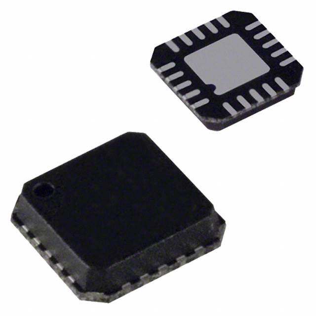
Data Sheet ADG1414 OUTLINE DIMENSIONS 7.90 7.80 7.70 24 13 4.50 4.40 4.30 6.40 BSC 1 12 PIN 1 0.65 1.20 BSC MAX 0.15 0.05 8° 0.75 0.30 SEATING 0.20 0° 0.60 0.19 PLANE 0.09 0.45 0.10 COPLANARITY COMPLIANT TO JEDEC STANDARDS MO-153-AD Figure 32. 24-Lead Thin Shrink Small Outline Package [TSSOP] (RU-24) Dimensions shown in millimeters 4.10 0.30 4.00 SQ 0.25 PIN 1 3.90 0.18 INDICATOR PIN 1 0.50 19 24 INDICATOR BSC 18 1 EXPOSED 2.65 PAD 2.50 SQ 2.45 13 6 0.50 12 7 0.25 MIN TOP VIEW BOTTOM VIEW 0.40 0.30 0.80 FOR PROPER CONNECTION OF 0.75 0.05 MAX THE EXPOSED PAD, REFER TO 0.70 0.02 NOM THE PIN CONFIGURATION AND FUNCTION DESCRIPTIONS COPLANARITY SECTION OF THIS DATA SHEET. SEATING 0.08 PLANE COMPLIANTTOJED0E.2C0 SRTEAFNDARDS MO-220-WGGD. 03-11-2013-A Figure 33. 24-Lead Lead Frame Chip Scale Package [LFCSP] 4 mm × 4 mm Body and 0.75 mm Package Height (CP-24-7) Dimensions shown in millimeters ORDERING GUIDE Model1 Temperature Range Package Description Package Option ADG1414BRUZ −40°C to +125°C 24-Lead Thin Shrink Small Outline Package [TSSOP] RU-24 ADG1414BRUZ-REEL7 −40°C to +125°C 24-Lead Thin Shrink Small Outline Package [TSSOP] RU-24 ADG1414BCPZ-REEL7 −40°C to +125°C 24-Lead Lead Frame Chip Scale Package [LFCSP] CP-24-7 1 Z = RoHS Compliant Part. ©2009–2015 Analog Devices, Inc. All rights reserved. Trademarks and registered trademarks are the property of their respective owners. D08497-0-11/15(B) Rev. B | Page 19 of 19
Mouser Electronics Authorized Distributor Click to View Pricing, Inventory, Delivery & Lifecycle Information: A nalog Devices Inc.: ADG1414BRUZ ADG1414BRUZ-REEL7 ADG1414BCPZ-REEL7 EVAL-24TSSOPEBZ