ICGOO在线商城 > 射频/IF 和 RFID > RF 收发器 IC > ADF7021BCPZ-RL7
 Datasheet下载
- 型号: ADF7021BCPZ-RL7
- 制造商: Analog
- 库位|库存: xxxx|xxxx
- 要求:
| 数量阶梯 | 香港交货 | 国内含税 |
| +xxxx | $xxxx | ¥xxxx |
查看当月历史价格
查看今年历史价格
ADF7021BCPZ-RL7产品简介:
ICGOO电子元器件商城为您提供ADF7021BCPZ-RL7由Analog设计生产,在icgoo商城现货销售,并且可以通过原厂、代理商等渠道进行代购。 ADF7021BCPZ-RL7价格参考¥25.83-¥47.57。AnalogADF7021BCPZ-RL7封装/规格:RF 收发器 IC, IC 射频 仅限 TxRx 通用 ISM < 1GHz 80MHz ~ 650MHz,862MHz ~ 950MHz 48-VFQFN 裸露焊盘,CSP。您可以下载ADF7021BCPZ-RL7参考资料、Datasheet数据手册功能说明书,资料中有ADF7021BCPZ-RL7 详细功能的应用电路图电压和使用方法及教程。
ADF7021BCPZ-RL7是由Analog Devices Inc.(ADI公司)生产的一款RF收发器IC,广泛应用于低功耗、短距离无线通信系统。以下是其主要应用场景:

 1. 智能家居与自动化
ADF7021BCPZ-RL7适用于各种智能家居设备,如智能门锁、智能灯控、温控器等。它能够实现设备之间的低功耗无线通信,帮助构建高效的物联网(IoT)网络。通过其灵活的调制方式和较低的功耗,该芯片可以延长电池寿命,特别适合那些需要长时间运行而无需频繁更换电池的设备。

 2. 工业控制与监测
在工业环境中,ADF7021BCPZ-RL7可用于无线传感器网络(WSN),如温度、湿度、压力等传感器的数据传输。它支持多种调制方式(如FSK、GFSK、MSK等),能够在复杂的工业环境下提供稳定可靠的通信。此外,该芯片的工作频率范围较广(315 MHz至915 MHz),适应不同国家和地区的频段要求。

 3. 医疗健康设备
该芯片也可用于便携式医疗设备,如心率监测仪、血糖仪等。这些设备通常需要低功耗和小尺寸的设计,ADF7021BCPZ-RL7正好满足这些需求。它可以通过无线方式将数据传输到智能手机或其他终端设备,方便用户实时监控健康状况。

 4. 消费电子
在消费电子产品中,ADF7021BCPZ-RL7可用于遥控器、无线耳机、玩具等设备。它支持低功耗模式,可以在待机状态下保持极低的电流消耗,从而延长电池寿命。同时,其集成度高,减少了外围电路的设计复杂度,降低了整体成本。

 5. 农业与环境监测
在农业领域,ADF7021BCPZ-RL7可用于土壤湿度传感器、气象站等设备,帮助农民进行精准农业管理。它能够将采集到的数据无线传输到中央控制系统,实现远程监控和自动化管理。此外,在环境监测方面,该芯片也适用于空气质量监测、水质检测等应用。

总之,ADF7021BCPZ-RL7凭借其低功耗、高集成度和灵活性,广泛应用于多个领域,特别是在需要低功耗、短距离无线通信的场景中表现出色。
| 参数 | 数值 |
| 产品目录 | |
| 描述 | IC TXRX ISM HI PERFORM 48-LFCSP射频收发器 High Performance Narrow-Band IC |
| 产品分类 | RF 收发器集成电路 - IC |
| 品牌 | Analog Devices Inc |
| 产品手册 | |
| 产品图片 |
|
| rohs | 符合RoHS无铅 / 符合限制有害物质指令(RoHS)规范要求 |
| 产品系列 | RF集成电路,射频收发器,Analog Devices ADF7021BCPZ-RL7- |
| 数据手册 | |
| 产品型号 | ADF7021BCPZ-RL7 |
| PCN组件/产地 | |
| 产品培训模块 | http://www.digikey.cn/PTM/IndividualPTM.page?site=cn&lang=zhs&ptm=12876 |
| 产品种类 | 射频收发器 |
| 传输供电电流 | 13.5 mA |
| 功率-输出 | -16dBm ~ 13dBm |
| 包装 | Digi-Reel® |
| 商标 | Analog Devices |
| 天线连接器 | PCB,表面贴装 |
| 存储容量 | - |
| 安装风格 | SMD/SMT |
| 封装 | Reel |
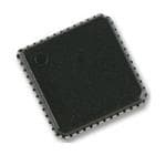
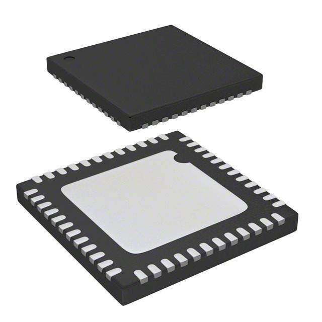
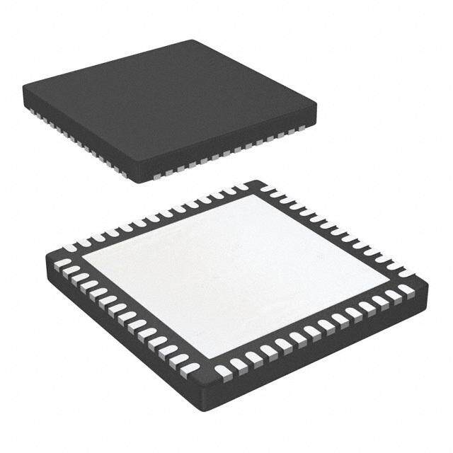
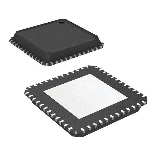
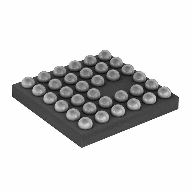
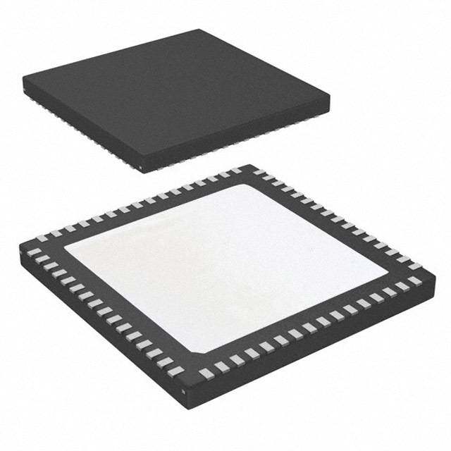
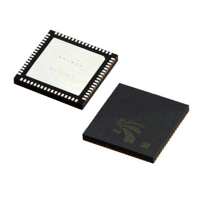
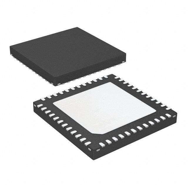
| 封装/外壳 | 48-VFQFN 裸露焊盘,CSP |
| 封装/箱体 | LFCSP EP |
| 工作温度 | -40°C ~ 85°C |
| 工作电源电压 | 3 V |
| 工厂包装数量 | 750 |
| 应用 | 无匙门禁系统,传呼机,WMTS |
| 接收供电电流 | 17.5 mA |
| 数据接口 | PCB,表面贴装 |
| 数据速率(最大值) | 33kbps |
| 最大工作温度 | + 85 C |
| 最大数据速率 | 32.8 kbps |
| 最小工作温度 | - 40 C |
| 标准包装 | 1 |
| 灵敏度 | -130dBm |
| 电压-电源 | 2.3 V ~ 3.6 V |
| 电流-传输 | 32.3mA @ 10dBm |
| 电流-接收 | 22.7mA |
| 电源电压-最大 | 3.6 V |
| 电源电压-最小 | 2.3 V |
| 系列 | ADF7021 |
| 视频文件 | http://www.digikey.cn/classic/video.aspx?PlayerID=1364138032001&width=640&height=505&videoID=2245193150001 |
| 调制或协议 | 2-FSK,3-FSK,4-FSK,MSK |
| 输出功率 | - 16 dBm to + 13 dBm |
| 频率 | 80MHz ~ 650MHz,862MHz ~ 940MHz |
| 频率范围 | 862 MHz to 950 MHz |

.jpg)


- 商务部:美国ITC正式对集成电路等产品启动337调查
- 曝三星4nm工艺存在良率问题 高通将骁龙8 Gen1或转产台积电
- 太阳诱电将投资9.5亿元在常州建新厂生产MLCC 预计2023年完工
- 英特尔发布欧洲新工厂建设计划 深化IDM 2.0 战略
- 台积电先进制程称霸业界 有大客户加持明年业绩稳了
- 达到5530亿美元!SIA预计今年全球半导体销售额将创下新高
- 英特尔拟将自动驾驶子公司Mobileye上市 估值或超500亿美元
- 三星加码芯片和SET,合并消费电子和移动部门,撤换高东真等 CEO
- 三星电子宣布重大人事变动 还合并消费电子和移动部门
- 海关总署:前11个月进口集成电路产品价值2.52万亿元 增长14.8%

PDF Datasheet 数据手册内容提取
High Performance Narrow-Band Transceiver IC Data Sheet ADF7021 FEATURES On-chip VCO and fractional-N PLL On-chip, 7-bit ADC and temperature sensor Low power, narrow-band transceiver Fully automatic frequency control loop (AFC) Frequency bands using dual VCO Digital received signal strength indication (RSSI) 80 MHz to 650 MHz Integrated Tx/Rx switch 862 MHz to 950 MHz 0.1 μA leakage current in power-down mode Modulation schemes 2FSK, 3FSK, 4FSK, MSK APPLICATIONS Spectral shaping Narrow-band standards Gaussian and raised cosine filtering ETSI EN 300 220, FCC Part 15, FCC Part 90, FCC Part 95, Data rates supported ARIB STD-T67 0.05 kbps to 32.8 kbps Low cost, wireless data transfer 2.3 V to 3.6 V power supply Remote control/security systems Programmable output power Wireless metering −16 dBm to +13 dBm in 63 steps Private mobile radio Automatic PA ramp control Wireless medical telemetry service (WMTS) Receiver sensitivity Keyless entry −130 dBm at 100 bps, 2FSK Home automation −122 dBm at 1 kbps, 2FSK Process and building control −113 dBm at 25 kbps, raised cosine 2FSK Pagers Patent pending, on-chip image rejection calibration FUNCTIONAL BLOCK DIAGRAM RSET CE CREG(1:4) MUXOUT TEMP RLNA SENSOR MUX 7-BITADC LDO(1:4) TESTMUX 2FSK LNA 3FSK CLOCK TxRxCLK RFIN RSSI/ 4FSK AND DATA Tx/Rx TxRxDATA RFINB IFFILTER LOG AMP RECOVERY CONTROL DEMODULATOR SWD GAIN AGC CONTROL SLE SERIAL SDATA PORT SREAD AFC PA RAMP CONTROL SCLK 2FSK GAUSSIAN/ RFOUT ÷1/÷2 DIVP N/N+1 Σ-∆ 3FSK RAISED COSINE MODULATOR 4FSK FILTER MODCONTROL ÷2 VCO1 3FSK ENCODING MUX CP PFD VCO2 CLK DIVR OSC DIV L1 L2 VCOIN CPOUT OSC1 OSC2 CLKOUT 05876-001 Figure 1. Rev. D Document Feedback Information furnished by Analog Devices is believed to be accurate and reliable. However, no responsibility is assumed by Analog Devices for its use, nor for any infringements of patents or other One Technology Way, P.O. Box 9106, Norwood, MA 02062-9106, U.S.A. rights of third parties that may result from its use. Specifications subject to change without notice. No license is granted by implication or otherwise under any patent or patent rights of Analog Devices. Tel: 781.329.4700 ©2007–2016 Analog Devices, Inc. All rights reserved. Trademarks and registered trademarks are the property of their respective owners. Technical Support www.analog.com
ADF7021 Data Sheet TABLE OF CONTENTS Features .............................................................................................. 1 Receiver Setup ............................................................................. 34 Applications ....................................................................................... 1 Demodulator Considerations ................................................... 36 Functional Block Diagram .............................................................. 1 AFC Operation ........................................................................... 36 Revision History ............................................................................... 3 Automatic Sync Word Detection (SWD) ................................ 37 General Description ......................................................................... 4 Applications Information .............................................................. 38 Specifications ..................................................................................... 5 IF Filter Bandwidth Calibration ............................................... 38 RF and PLL Specifications ........................................................... 5 LNA/PA Matching ...................................................................... 38 Transmission Specifications ........................................................ 6 Image Rejection Calibration ..................................................... 39 Receiver Specifications ................................................................ 8 Packet Structure and Coding .................................................... 41 Digital Specifications ................................................................. 10 Applications Circuit ................................................................... 44 General Specifications ............................................................... 11 Serial Interface ................................................................................ 45 Timing Characteristics .............................................................. 11 Readback Format ........................................................................ 45 Absolute Maximum Ratings .......................................................... 15 Interfacing to Microcontroller/DSP ........................................ 46 ESD Caution ................................................................................ 15 Register 0—N Register ............................................................... 47 Pin Configuration and Function Descriptions ........................... 16 Register 1—VCO/Oscillator Register ...................................... 47 Typical Performance Characteristics ........................................... 18 Register 2—Transmit Modulation Register ............................ 49 Frequency Synthesizer ................................................................... 22 Register 3—Transmit/Receive Clock Register ........................ 50 Reference Input ........................................................................... 22 Register 4—Demodulator Setup Register ............................... 51 MUXOUT .................................................................................... 23 Register 5—IF Filter Setup Register ......................................... 52 Voltage Controlled Oscillator (VCO) ...................................... 24 Register 6—IF Fine Cal Setup Register ................................... 53 Choosing Channels for Best System Performance ................. 25 Register 7—Readback Setup Register ...................................... 54 Transmitter ...................................................................................... 26 Register 8—Power-Down Test Register .................................. 55 RF Output Stage .......................................................................... 26 Register 9—AGC Register ......................................................... 56 Modulation Schemes .................................................................. 26 Register 10—AFC Register ....................................................... 57 Spectral Shaping ......................................................................... 28 Register 11—Sync Word Detect Register ................................ 58 Modulation and Filtering Options ........................................... 29 Register 12—SWD/Threshold Setup Register ........................ 58 Transmit Latency ........................................................................ 29 Register 13—3FSK/4FSK Demod Register ............................. 59 Test Pattern Generator ............................................................... 29 Register 14—Test DAC Register ............................................... 60 Receiver Section .............................................................................. 30 Register 15—Test Mode Register ............................................. 61 RF Front End ............................................................................... 30 Outline Dimensions ....................................................................... 62 IF Filter ........................................................................................ 30 Ordering Guide .......................................................................... 62 RSSI/AGC .................................................................................... 31 Demodulation, Detection, and CDR ....................................... 32 Rev. D | Page 2 of 62
Data Sheet ADF7021 REVISION HISTORY 9/2016—Rev. C to Rev. D 9/2007—Rev. 0 to Rev. A Changes to General Description Section ....................................... 4 Change to UART/SPI Mode Section ............................................ 14 Changes to Interfacing to Microcontroller/DSP Section and Changes to Figure 10 ...................................................................... 16 Figure 58 ........................................................................................... 46 Change to Table 8 ............................................................................ 16 Changes to Figure 12 ...................................................................... 18 10/2014—Rev. B to Rev. C Change to Internal Inductor VCO Section .................................. 24 Changes to Table 8 .......................................................................... 16 Changes to Figure 40 ...................................................................... 26 Change to Figure 36 ........................................................................ 24 Changes to Figure 47 ...................................................................... 32 Change to IF Filter Fine Calibration Overview Section ............ 30 Change to Table 19 .......................................................................... 34 Change to Post Demodulator Filter Setup Section ..................... 34 Changes to Figure 56 ...................................................................... 44 Change to Battery Voltage/ADCIN/Temperature Sensor Change to SPI Mode Section ......................................................... 46 Readback Section ............................................................................ 45 Changes to Figure 59 ...................................................................... 46 Change to Register 4—Demodulator Setup Register Section ... 51 Changes to Figure 60 ...................................................................... 46 Change to Register 7—Readback Setup Register Section .......... 54 Change to Register 3—Transmit/Receive Clock Change to Register 10—AFC Register Section ........................... 57 Register Section ............................................................................... 50 Change to Register 4—Demodulator Setup Register Section ......... 51 4/2013—Rev. A to Rev. B Change to Register 7—Readback Setup Register ........................ 54 Changes to Figure 10 ...................................................................... 16 Change to Register 13—3FSK/4FSK Demod Register Heading .... 59 Updated Outline Dimensions ........................................................ 62 Changes to Ordering Guide ........................................................... 62 3/2007—Revision 0: Initial Version Rev. D | Page 3 of 62
ADF7021 Data Sheet GENERAL DESCRIPTION The ADF7021 is a high performance, low power, highly integrated The transmitter output power is programmable in 63 steps from 2FSK/3FSK/4FSK transceiver. It is designed to operate in the −16 dBm to +13 dBm, and has an automatic power ramp control to narrowband, license-free ISM bands, and in the licensed bands prevent spectral splatter and help meet regulatory standards. with frequency ranges of 80 MHz to 650 MHz and 862 MHz to The transceiver RF frequency and modulation are programmable 950 MHz. The device has both Gaussian and raised cosine transmit using a simple 3-wire interface. The device operates with a power data filtering options to improve spectral efficiency for narrow- supply range of 2.3 V to 3.6 V and can be powered down when band applications. It is suitable for circuit applications targeted not in use. at European ETSI EN 300 220, the Japanese ARIB STD-T67, the A low IF architecture is used in the receiver (100 kHz), which Chinese short range device regulations, and the North American minimizes power consumption and the external component FCC Part 15, Part 90, and Part 95 regulatory standards. A complete count, yet avoids dc offset and flicker noise at low frequencies. The transceiver can be built using a small number of external discrete IF filter has programmable bandwidths of 12.5 kHz, 18.75 kHz, and components, making the ADF7021 very suitable for price 25 kHz. The ADF7021 supports a wide variety of programmable sensitive and area sensitive applications. features including Rx linearity, sensitivity, and IF bandwidth, The range of on-chip FSK modulation and data filtering options allowing the user to trade off receiver sensitivity and selectivity allows users greater flexibility in their choice of modulation against current consumption, depending on the application. schemes while meeting tight spectral efficiency requirements. The receiver also features a patent-pending automatic frequency The ADF7021 also supports protocols that dynamically switch control (AFC) loop with programmable pull-in range that allows between 2FSK/3FSK/4FSK to maximize communication range the PLL to track out the frequency error in the incoming signal. and data throughput. The receiver achieves an image rejection performance of 56 dB The transmit section contains dual voltage controlled oscillators using a patent-pending IR calibration scheme that does not (VCOs) and a low noise fractional-N PLL with an output resolution require the use of an external RF source. of <1 ppm. The ADF7021 has a VCO using an internal LC tank An on-chip ADC provides readback of the integrated temperature (431 MHz to 475 MHz, 862 MHz to 950 MHz) and a VCO using sensor, external analog input, battery voltage, and RSSI signal, an external inductor as part of its tank circuit (80 MHz to which provides savings on an ADC in some applications. The 650 MHz). The dual VCO design allows dual-band operation temperature sensor is accurate to ±10°C over the full operating where the user can transmit and/or receive at any frequency temperature range of −40°C to +85°C. This accuracy can be supported by the internal inductor VCO and can also transmit improved by performing a 1-point calibration at room and/or receive at a particular frequency band supported by the temperature and storing the result in memory. external inductor VCO. The frequency agile PLL allows the ADF7021 to be used in frequency hopping spread spectrum (FHSS) systems. Both VCOs operate at twice the fundamental frequency to reduce spurious emissions and frequency pulling problems. Rev. D | Page 4 of 62
Data Sheet ADF7021 SPECIFICATIONS V = 2.3 V to 3.6 V, GND = 0 V, T = T to T , unless otherwise noted. Typical specifications are at V = 3 V, T = 25°C. All DD A MIN MAX DD A measurements are performed with the EVAL-ADF7021DB evaluation boards using the PN9 data sequence, unless otherwise noted. RF AND PLL SPECIFICATIONS Table 1. Parameter Min Typ Max Unit Test Conditions/Comments RF CHARACTERISTICS See Table 9 for required VCO_BIAS and VCO_ADJUST settings Frequency Ranges (Direct Output) 160 650 MHz External inductor VCO 862 950 MHz Internal inductor VCO Frequency Ranges (RF Divide-by-2 Mode) 80 325 MHz External inductor VCO, RF divide-by-2 enabled 431 475 MHz Internal inductor VCO, RF divide-by-2 enabled Phase Frequency Detector (PFD) Frequency1 RF/256 26/30 MHz Crystal reference/external reference PHASE-LOCKED LOOP (PLL) VCO Gain2 868 MHz, Internal Inductor VCO 58 MHz/V VCO_ADJUST = 0, VCO_BIAS = 8 434 MHz, Internal Inductor VCO 29 MHz/V VCO_ADJUST = 0, VCO_BIAS = 8 426 MHz, External Inductor VCO 27 MHz/V VCO_ADJUST = 0, VCO_BIAS = 3 160 MHz, External Inductor VCO 6 MHz/V VCO_ADJUST = 0, VCO_BIAS = 2 Phase Noise (In-Band) 868 MHz, Internal Inductor VCO −97 dBc/Hz 10 kHz offset, PA = 10 dBm, V = 3.0 V, DD PFD = 19.68 MHz, VCO_BIAS = 8 433 MHz, Internal Inductor VCO −103 dBc/Hz 10 kHz offset, PA = 10 dBm, V = 3.0 V, DD PFD = 19.68 MHz, VCO_BIAS = 8 426 MHz, External Inductor VCO −95 dBc/Hz 10 kHz offset, PA = 10 dBm, V = 3.0 V, DD PFD = 9.84 MHz, VCO_BIAS = 3 Phase Noise (Out-of-Band) −124 dBc/Hz 1 MHz offset, f = 433 MHz, PA = 10 dBm, RF V = 3.0 V, PFD = 19.68 MHz, VCO_BIAS = 8 DD Normalized In-Band Phase Noise Floor3 −203 dBc/Hz PLL Settling 40 µs Measured for a 10 MHz frequency step to within 5 ppm accuracy, PFD = 19.68 MHz, loop bandwidth (LBW) = 100 kHz REFERENCE INPUT Crystal Reference4 3.625 26 MHz External Oscillator4, 5 3.625 30 MHz Crystal Start-Up Time6 XTAL Bias = 20 µA 0.930 ms 10 MHz XTAL, 33 pF load capacitors, V = 3.0 V DD XTAL Bias = 35 µA 0.438 ms 10 MHz XTAL, 33 pF load capacitors, V = 3.0 V DD Input Level for External Oscillator7 OSC1 0.8 V p-p Clipped sine wave OSC2 CMOS levels V ADC PARAMETERS INL ±0.4 LSB V = 2.3 V to 3.6 V, T = 25°C DD A DNL ±0.4 LSB V = 2.3 V to 3.6 V, T = 25°C DD A 1 The maximum usable PFD at a particular RF frequency is limited by the minimum N divide value. 2 VCO gain measured at a VCO tuning voltage of 1 V. The VCO gain varies across the tuning range of the VCO. The software package ADIsimPLL™ can be used to model this variation. 3 This value can be used to calculate the in-band phase noise for any operating frequency. Use the following equation to calculate the in-band phase noise performance as seen at the PA output: −203 + 10 log(fPFD) + 20 logN. 4 Guaranteed by design. Sample tested to ensure compliance. 5 A TCXO, VCXO, or OCXO can be used as an external oscillator. 6 Crystal start-up time is the time from chip enable (CE) being asserted to correct clock frequency on the CLKOUT pin. 7 Refer to the Reference Input section for details on using an external oscillator. Rev. D | Page 5 of 62
ADF7021 Data Sheet TRANSMISSION SPECIFICATIONS Table 2. Parameter Min Typ Max Unit Test Conditions/Comments DATA RATE 2FSK, 3FSK 0.05 251 kbps IF_BW = 25 kHz 4FSK 0.05 32.82 kbps IF_BW = 25 kHz MODULATION Frequency Deviation (fDEV)3 0.056 28.26 kHz PFD = 3.625 MHz 0.306 156 kHz PFD = 20 MHz Deviation Frequency Resolution 56 Hz PFD = 3.625 MHz Gaussian Filter BT 0.5 Raised Cosine Filter Alpha 0.5/0.7 Programmable TRANSMIT POWER Maximum Transmit Power4 +13 dBm VDD = 3.0 V, TA = 25°C Transmit Power Variation vs. ±1 dB −40°C to +85°C Temperature Transmit Power Variation vs. V ±1 dB 2.3 V to 3.6 V at 915 MHz, T = 25°C DD A Transmit Power Flatness ±1 dB 902 MHz to 928 MHz, 3 V, T = 25°C A Programmable Step Size 0.3125 dB −20 dBm to +13 dBm ADJACENT CHANNEL POWER (ACP) 426 MHz, External Inductor VCO PFD = 9.84 MHz 12.5 kHz Channel Spacing −50 dBc Gaussian 2FSK modulation, measured in a ±4.25 kHz bandwidth at ±12.5 kHz offset, 2.4 kbps PN9 data, 1.2 kHz frequency deviation, compliant with ARIB STD-T67 25 kHz Channel Spacing −50 dBc Gaussian 2FSK modulation, measured in a ±8 kHz bandwidth at ±25 kHz offset, 9.6 kbps PN9 data, 2.4 kHz frequency deviation, compliant with ARIB STD-T67 868 MHz, Internal Inductor VCO PFD = 19.68 MHz 12.5 kHz Channel Spacing −46 dBm Gaussian 2FSK modulation, 10 dBm output power, measured in a ±6.25 kHz bandwidth at ±12.5 kHz offset, 2.4 kbps PN9 data, 1.2 kHz frequency deviation, compliant with ETSI EN 300-220 25 kHz Channel Spacing −43 dBm Gaussian 2FSK modulation, 10 dBm output power, measured in a ±12.5 kHz bandwidth at ±25 kHz offset, 9.6 kbps PN9 data, 2.4 kHz frequency deviation, compliant with ETSI EN 300-220 433 MHz, Internal Inductor VCO PFD = 19.68 MHz 12.5 kHz Channel Spacing −50 dBm Gaussian 2FSK modulation, 10 dBm output power, measured in a ±6.25 kHz bandwidth at ±12.5 kHz offset, 2.4 kbps PN9 data, 1.2 kHz frequency deviation, compliant with ETSI EN 300-220 25 kHz Channel Spacing −47 dBm Gaussian 2FSK modulation, 10 dBm output power, measured in a ±12.5 kHz bandwidth at ±25 kHz offset, 9.6 kbps PN9 data, 2.4 kHz frequency deviation, compliant with ETSI EN 300-220 OCCUPIED BANDWIDTH 99.0% of total mean power; 12.5 kHz channel spacing (2.4 kbps PN9 data, 1.2 kHz frequency deviation); 25 kHz channel spacing (9.6 kbps PN9 data, 2.4 kHz frequency deviation) 2FSK Gaussian Data Filtering 12.5 kHz Channel Spacing 3.9 kHz 25 kHz Channel Spacing 9.9 kHz 2FSK Raised Cosine Data Filtering 12.5 kHz Channel Spacing 4.4 kHz 25 kHz Channel Spacing 10.2 kHz 3FSK Raised Cosine Filtering 12.5 kHz Channel Spacing 3.9 kHz 25 kHz Channel Spacing 9.5 kHz 4FSK Raised Cosine Filtering 19.2 kbps PN9 data, 1.2 kHz frequency deviation 25 kHz Channel Spacing 13.2 kHz Rev. D | Page 6 of 62
Data Sheet ADF7021 Parameter Min Typ Max Unit Test Conditions/Comments SPURIOUS EMISSIONS Reference Spurs −65 dBc 100 kHz loop bandwidth HARMONICS5 13 dBm output power, unfiltered conductive/filtered conductive Second Harmonic −35/−52 dBc Third Harmonic −43/−60 dBc All Other Harmonics −36/−65 dBc OPTIMUM PA LOAD IMPEDANCE6 f = 915 MHz 39 + j61 Ω RF f = 868 MHz 48 + j54 Ω RF f = 450 MHz 98 + j65 Ω RF f = 426 MHz 100 + j65 Ω RF f = 315 MHz 129 + j63 Ω RF f = 175 MHz 173 + j49 Ω RF 1 Using Gaussian or raised cosine filtering. Choose the frequency deviation to ensure that the transmit occupied signal bandwidth is within the receiver IF filter bandwidth. 2 Using raised cosine filtering with an alpha = 0.7. The inner frequency deviation = 1.78 kHz, and the POST_DEMOD_BW = 24.6 kHz. 3 For the definition of frequency deviation, refer to the Register 2—Transmit Modulation Register section. 4 Measured as maximum unmodulated power. 5 Conductive filtered harmonic emissions measured on the EVAL-ADF7021DB models, which includes a T-stage harmonic filter (two inductors and one capacitor). 6 For matching details, refer to the LNA/PA Matching section. Rev. D | Page 7 of 62
ADF7021 Data Sheet RECEIVER SPECIFICATIONS Table 3. Parameter Min Typ Max Unit Test Conditions/Comments SENSITIVITY Bit error rate (BER) = 10−3, low noise amplifier (LNA) and power amplifier (PA) matched separately 2FSK Sensitivity at 0.1 kbps −130 dBm f = 1 kHz, high sensitivity mode, IF_BW = 12.5 kHz DEV Sensitivity at 0.25 kbps −127 dBm f = 1 kHz, high sensitivity mode, IF_BW = 12.5 kHz DEV Sensitivity at 1 kbps −122 dBm f = 1 kHz, high sensitivity mode, IF_BW = 12.5 kHz DEV Sensitivity at 9.6 kbps −115 dBm f = 4 kHz, high sensitivity mode, IF_BW = 18.75 kHz DEV Sensitivity at 25 kbps −110 dBm f = 10 kHz, high sensitivity mode, IF_BW = 25 kHz DEV Gaussian 2FSK Sensitivity at 0.1 kbps −129 dBm f = 1 kHz, high sensitivity mode, IF_BW = 12.5 kHz DEV Sensitivity at 0.25 kbps −127 dBm f = 1 kHz, high sensitivity mode, IF_BW = 12.5 kHz DEV Sensitivity at 1 kbps −121 dBm f = 1 kHz, high sensitivity mode, IF_BW = 12.5 kHz DEV Sensitivity at 9.6 kbps −114 dBm f = 4 kHz, high sensitivity mode, IF_BW = 18.75 kHz DEV Sensitivity at 25 kbps −111 dBm f = 10 kHz, high sensitivity mode, IF_BW = 25 kHz DEV GMSK Sensitivity at 9.6 kbps −113 dBm f = 2.4 kHz, high sensitivity mode, IF_BW = 18.75 kHz DEV Raised Cosine 2FSK Sensitivity at 0.25 kbps −127 dBm f = 1 kHz, high sensitivity mode, IF_BW = 12.5 kHz DEV Sensitivity at 1 kbps −121 dBm f = 1 kHz, high sensitivity mode, IF_BW = 12.5 kHz DEV Sensitivity at 9.6 kbps −114 dBm f = 4 kHz, high sensitivity mode, IF_BW = 18.75 kHz DEV Sensitivity at 25 kbps −113 dBm f = 10 kHz, high sensitivity mode, IF_BW = 25 kHz DEV 3FSK Sensitivity at 9.6 kbps −110 dBm f = 2.4 kHz, high sensitivity mode, IF_BW = 18.75 kHz, DEV Viterbi detection on Raised Cosine 3FSK Sensitivity at 9.6 kbps −110 dBm f = 2.4 kHz, high sensitivity mode, IF_BW = 12.5 kHz, DEV alpha = 0.5, Viterbi detection on Sensitivity at 19.6 kbps −106 dBm f = 4.8 kHz, high sensitivity mode, IF_BW = 18.75 kHz, DEV alpha = 0.5, Viterbi detection on 4FSK Sensitivity at 9.6 kbps −112 dBm f (inner) = 1.2 kHz, high sensitivity mode, IF_BW = 12.5 kHz DEV Sensitivity at 19.6 kbps −107 dBm f (inner) = 2.4 kHz, high sensitivity mode, IF_BW = 25 kHz DEV Raised Cosine 4FSK Sensitivity at 9.6 kbps −109 dBm f (inner) = 1.2 kHz, high sensitivity mode, DEV IF_BW = 12.5 kHz, alpha = 0.5 Sensitivity at 19.2 kbps −103 dBm f (inner) = 1.2 kHz, high sensitivity mode, DEV IF_BW = 18.75 kHz, alpha = 0.5 Sensitivity at 32.8 kbps −100 dBm f (inner) = 1.8 kHz, high sensitivity mode, IF_BW = 25 kHz, DEV alpha = 0.7 INPUT IP3 Two-tone test, f = 860 MHz, F1 = f + 100 kHz, F2 = f − 800 kHz LO LO LO Low Gain Enhanced Linearity −3 dBm LNA_GAIN = 3, MIXER_LINEARITY = 1 Mode Medium Gain Mode −13.5 dBm LNA_GAIN = 10, MIXER_LINEARITY = 0 High Sensitivity Mode −24 dBm LNA_GAIN = 30, MIXER_LINEARITY = 0 Rev. D | Page 8 of 62
Data Sheet ADF7021 Parameter Min Typ Max Unit Test Conditions/Comments ADJACENT CHANNEL REJECTION 868 MHz Wanted signal is 3 dB above the sensitivity point (BER = 10−3); unmodulated interferer is at the center of the adjacent channel; rejection measured as the difference between interferer level and wanted signal level in dB 12.5 kHz Channel Spacing 25 dB 12.5 kHz IF_BW 25 kHz Channel Spacing 27 dB 25 kHz IF_BW 25 kHz Channel Spacing 39 dB 18 kHz IF_BW 426 MHz, External Inductor VCO Wanted signal 3 dB above reference sensitivity point (BER = 10−2); modulated interferer (1 kHz sine, ±2 kHz deviation) at the center of the adjacent channel; rejection measured as the difference between interferer level and reference sensitivity level in dB 12.5 kHz Channel Spacing 25 dB 12.5 kHz IF_BW 25 kHz Channel Spacing 30 dB 25 kHz IF_BW 25 kHz Channel Spacing 41 dB 18 kHz IF_BW, compliant with ARIB STD-T67 CO-CHANNEL REJECTION Wanted signal (2FSK, 9.6 kbps, ±4 kHz deviation) is 10 dB above the sensitivity point (BER = 10−3), modulated interferer 868 MHz −3 dB IMAGE CHANNEL REJECTION Wanted signal (2FSK, 9.6 kbps, ±4 kHz deviation) is 10 dB above the sensitivity point (BER = 10−3); modulated interferer (2FSK, 9.6 kbps, ±4 kHz deviation) is placed at the image frequency of f − 200 kHz; interferer level is increased until RF BER = 10−3 900 MHz 23/39 dB Uncalibrated/calibrated1, V = 3.0 V, T = 25°C DD A 450 MHz 29/50 dB Uncalibrated/calibrated1,V = 3.0 V, T = 25°C DD A 450 MHz, External Inductor VCO 38/53 dB Uncalibrated/calibrated1, V = 3.0 V, T = 25°C DD A BLOCKING Wanted signal is 10 dB above the input sensitivity level; CW interferer level is increased until BER = 10−3 ±1 MHz 69 dB ±2 MHz 75 dB ±5 MHz 78 dB ±10 MHz 78.5 dB SATURATION 12 dBm 2FSK mode, BER = 10−3 (MAXIMUM INPUT LEVEL) RSSI Range at Input2 −120 to dBm −47 Linearity ±2 dB Input power range = −100 dBm to −47 dBm Absolute Accuracy ±3 dB Input power range = −100 dBm to −47 dBm Response Time 300 µs See the RSSI/AGC section AFC Pull-In Range 0.5 1.5 × IF_BW kHz The range is programmable, R10_DB[24:31] Response Time 48 Bits Accuracy 0.5 kHz Input power range = −100 dBm to +12 dBm Rx SPURIOUS EMISSIONS3 Internal Inductor VCO −91/−91 dBm <1 GHz at antenna input, unfiltered conductive/filtered conductive −52/−70 dBm >1 GHz at antenna input, unfiltered conductive/filtered conductive External Inductor VCO −62/−72 dBm <1 GHz at antenna input, unfiltered conductive/filtered conductive −64/−85 dBm >1 GHz at antenna input, unfiltered conductive/filtered conductive Rev. D | Page 9 of 62
ADF7021 Data Sheet Parameter Min Typ Max Unit Test Conditions/Comments LNA INPUT IMPEDANCE RFIN to RFGND f = 915 MHz 24 − j60 Ω RF f = 868 MHz 26 − j63 Ω RF f = 450 MHz 63 − j129 Ω RF f = 426 MHz 68 − j134 Ω RF f = 315 MHz 96 − j160 Ω RF f = 175 MHz 178 − j190 Ω RF 1 Calibration of the image rejection used an external RF source. 2 For received signal levels < −100 dBm, it is recommended to average the RSSI readback value over a number of samples to improve the RSSI accuracy at low input powers. 3 Filtered conductive receive spurious emissions measured on the EVAL-ADF7021DB evaluation boards, which includes a T-stage harmonic filter (two inductors and one capacitor). DIGITAL SPECIFICATIONS Table 4. Parameter Min Typ Max Unit Test Conditions/Comments TIMING INFORMATION Chip Enabled to Regulator Ready 10 µs C = 100 nF REG Chip Enabled to Tx Mode 32-bit register write time = 50 µs TCXO Reference 1 ms XTAL 2 ms Chip Enabled to Rx Mode 32-bit register write time = 50 µs, IF filter coarse calibration only TCXO Reference 1.2 ms XTAL 2.2 ms Tx to Rx Turnaround Time 300 µs + (5 × t ) Time to synchronized data out, includes AGC BIT settling and CDR synchronization; see AGC Information and Timing section for more details; t = data bit period BIT LOGIC INPUTS Input High Voltage, V 0.7 × V V INH DD Input Low Voltage, V 0.2 × V V INL DD Input Current, I /I ±1 µA INH INL Input Capacitance, C 10 pF IN Control Clock Input 50 MHz LOGIC OUTPUTS Output High Voltage, V DV − 0.4 V I = 500 µA OH DD OH Output Low Voltage, V 0.4 V I = 500 µA OL OL CLKOUT Rise/Fall 5 ns CLKOUT Load 10 pF Rev. D | Page 10 of 62
Data Sheet ADF7021 GENERAL SPECIFICATIONS Table 5. Parameter Min Typ Max Unit Test Conditions/Comments TEMPERATURE RANGE (T ) −40 +85 °C A POWER SUPPLIES Voltage Supply, V 2.3 3.6 V All VDD pins must be tied together DD TRANSMIT CURRENT CONSUMPTION1 V = 3.0 V, PA is matched into 50 Ω DD 868 MHz VCO_BIAS = 8 0 dBm 20.2 mA 5 dBm 24.7 mA 10 dBm 32.3 mA 450 MHz, Internal Inductor VCO VCO_BIAS = 8 0 dBm 19.9 mA 5 dBm 23.2 mA 10 dBm 29.2 mA 426 MHz, External Inductor VCO VCO_BIAS = 2 0 dBm 13.5 mA 5 dBm 17 mA 10 dBm 23.3 mA RECEIVE CURRENT CONSUMPTION V = 3.0 V DD 868 MHz VCO_BIAS = 8 Low Current Mode 22.7 mA High Sensitivity Mode 24.6 mA 433MHz, Internal Inductor VCO VCO_BIAS = 8 Low Current Mode 24.5 mA High Sensitivity Mode 26.4 mA 426 MHz, External Inductor VCO VCO_BIAS = 2 Low Current Mode 17.5 mA High Sensitivity Mode 19.5 mA POWER-DOWN CURRENT CONSUMPTION Low Power Sleep Mode 0.1 1 µA CE low 1 The transmit current consumption tests used the same combined PA and LNA matching network as that used on the EVAL-ADF7021DB evaluation boards. Improved PA efficiency is achieved by using a separate PA matching network. TIMING CHARACTERISTICS V = 3 V ± 10%, DGND = AGND = 0 V, T = 25°C, unless otherwise noted. Guaranteed by design but not production tested. DD A Table 6. Parameter Limit at T to T Unit Test Conditions/Comments MIN MAX t1 >10 ns SDATA to SCLK setup time t2 >10 ns SDATA to SCLK hold time t3 >25 ns SCLK high duration t4 >25 ns SCLK low duration t5 >10 ns SCLK to SLE setup time t6 >20 ns SLE pulse width t8 <25 ns SCLK to SREAD data valid, readback t9 <25 ns SREAD hold time after SCLK, readback t10 >10 ns SCLK to SLE disable time, readback t 5 < t < (¼ × t ) ns TxRxCLK negative edge to SLE 11 11 BIT t >5 ns TxRxDATA to TxRxCLK setup time (Tx mode) 12 t >5 ns TxRxCLK to TxRxDATA hold time (Tx mode) 13 t >¼ × t µs TxRxCLK negative edge to SLE 14 BIT t >¼ × t µs SLE positive edge to positive edge of TxRxCLK 15 BIT Rev. D | Page 11 of 62
ADF7021 Data Sheet Timing Diagrams Serial Interface t t 3 4 SCLK t t 1 2 DB1 DB0 (LSB) SDATA DB31 (MSB) DB30 DB2 (CONTROL BIT C2) (CONTROL BIT C1) t 6 SLE t5 05876-002 Figure 2. Serial Interface Timing Diagram t t 1 2 SCLK SDATA REG7 DB0 (CONTROL BIT C1) SLE t 3 t 10 SREAD X RV16 RV15 RV2 RV1 X t8 t9 05876-003 Figure 3. Serial Interface Readback Timing Diagram 2FSK/3FSK Timing ±1 × DATA RATE/32 1/DATA RATE TxRxCLK TxRxDATA DATA 05876-004 Figure 4. TxRxDATA/TxRxCLK Timing Diagram in Receive Mode 1/DATA RATE TxRxCLK TxRxDATA DATA FETCH SAMPLE 05876-005 Figure 5. TxRxDATA/TxRxCLK Timing Diagram in Transmit Mode Rev. D | Page 12 of 62
Data Sheet ADF7021 4FSK Timing In 4FSK receive mode, MSB/LSB synchronization is guaranteed by SWD in the receive bit stream. REGISTER 0 WRITE SWITCH FROM Rx TO Tx t SYMBOL t 13 t11 t12 t BIT SLE TxRxCLK Rx SYMBOL Rx SYMBOL Rx SYMBOL Rx SYMBOL Tx SYMBOL Tx SYMBOL Tx SYMBOL TxRxDATA MSB LSB MSB LSB MSB LSB MSB Tx/Rx MODE Rx MODE Tx MODE 05876-074 Figure 6. Receive-to-Transmit Timing Diagram in 4FSK Mode REGISTER 0 WRITE SWITCH FROM Tx TO Rx t15 tSYMBOL t 14 t BIT SLE TxRxCLK Tx SYMBOL Tx SYMBOL Tx SYMBOL Tx SYMBOL Rx SYMBOL Rx SYMBOL TxRxDATA MSB LSB MSB LSB MSB LSB Tx/Rx MODE Tx MODE Rx MODE 05876-075 Figure 7. Transmit-to-Receive Timing Diagram in 4FSK Mode Rev. D | Page 13 of 62
ADF7021 Data Sheet UART/SPI Mode UART mode is enabled by setting R0_DB28 to 1. SPI mode is enabled by setting R0_DB28 to 1 and setting R15_DB[17:19] to 0x7. The transmit/receive data clock is available on the CLKOUT pin. t BIT CLKOUT (TRANSMIT/RECEIVE DATA CLOCK IN SPI MODE. NOT USED IN UART MODE.) FETCH SAMPLE TxRxCLK (TRANSMIT DATA INPUT Tx BIT Tx BIT Tx BIT Tx BIT Tx BIT IN UART/SPI MODE.) TxRxDATA (RECEIVE DATA OUTPUT IN UART/SPI MODE.) HIGH-Z Tx/Rx MODE Tx MODE 05876-082 Figure 8. Transmit Timing Diagram in UART/SPI Mode t BIT CLKOUT (TRANSMIT/RECEIVE DATA CLOCK IN SPI MODE. NOT USED IN UART MODE.) FETCH SAMPLE TxRxCLK (TRANSMIT DATA INPUT HIGH-Z IN UART/SPI MODE.) TxRxDATA (RECEIVE DATA OUTPUT Rx BIT Rx BIT Rx BIT Rx BIT Rx BIT IN UART/SPI MODE.) Tx/Rx MODE Rx MODE 05876-078 Figure 9. Receive Timing Diagram in UART/SPI Mode Rev. D | Page 14 of 62
Data Sheet ADF7021 ABSOLUTE MAXIMUM RATINGS T = 25°C, unless otherwise noted. A Table 7. Stresses at or above those listed under Absolute Maximum Parameter Rating Ratings may cause permanent damage to the product. This is a V to GND1 −0.3 V to +5 V stress rating only; functional operation of the product at these DD Analog I/O Voltage to GND −0.3 V to AV + 0.3 V or any other conditions above those indicated in the operational DD Digital I/O Voltage to GND −0.3 V to DV + 0.3 V section of this specification is not implied. Operation beyond DD Operating Temperature Range the maximum operating conditions for extended periods may Industrial (B Version) −40°C to +85°C affect product reliability. Storage Temperature Range −65°C to +125°C This device is a high performance RF integrated circuit with an Maximum Junction Temperature 150°C ESD rating of <2 kV and it is ESD sensitive. Take proper MLF θJA Thermal Impedance 26°C/W precautions for handling and assembly. Reflow Soldering Peak Temperature 260°C Time at Peak Temperature 40 sec ESD CAUTION 1 GND = CPGND = RFGND = DGND = AGND = 0 V. Rev. D | Page 15 of 62
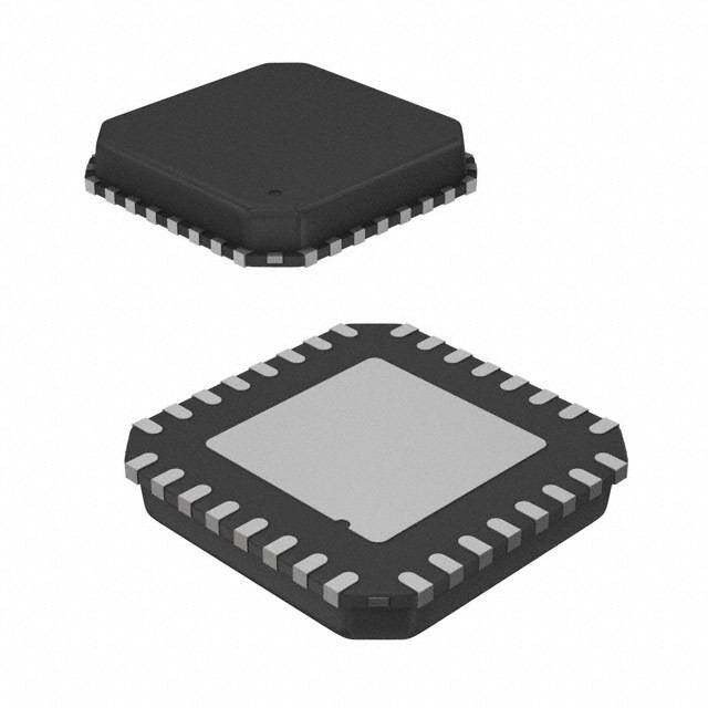
ADF7021 Data Sheet PIN CONFIGURATION AND FUNCTION DESCRIPTIONS T COD1 D DOUTEG3D3C1C2XOU CVGNL1GNL2VDCPCRVDOSOSMU 847464544434241404938373 VCOIN 1 36 CLKOUT CREG1 2 35 TxRxCLK VDD1 3 34 TxRxDATA RFOUT 4 33 SWD RFGND 5 ADF7021 32 VDD2 RFIN 6 TOP VIEW 31 CREG2 RFINB 7 (Not to Scale) 30 ADCIN RLNA 8 29 GND2 VDD4 9 28 SCLK RSET 10 27 SREAD CREG4 11 26 SDATA GND4 12 25 SLE 345678901234 111111122222 MIX_IMIX_IMIX_QMIX_QFILT_IFILT_IGND4FILT_QFILT_QGND4TEST_ACE N1.O TTHEES EXPOSEDPAD MUST BE CONNECTEDTO GND. 05876-006 Figure 10. Pin Configuration Table 8. Pin Function Descriptions Pin No. Mnemonic Description 1 VCOIN Regulator Voltage for PA Block and VCO Cores. The tuning voltage on this pin determines the output frequency of the voltage controlled oscillator (VCO). The higher the tuning voltage, the higher the output frequency. 2 CREG1 Regulator Voltage for PA Block. Place a series 3.9 Ω resistor and a 100 nF capacitor between this pin and ground for regulator stability and noise rejection. 3 VDD1 Voltage Supply for PA Block and VCO Cores. Place decoupling capacitors of 0.1 μF and 100 pF as close as possible to this pin. Tie all VDD pins together. 4 RFOUT The modulated signal is available at this pin. Output power levels are from −16 dBm to +13 dBm. Impedance match the output to the desired load using suitable components (see the Transmitter section). 5 RFGND Ground for Output Stage of Transmitter. Tie all GND pins together. 6 RFIN LNA Input for Receiver Section. Input matching is required between the antenna and the differential LNA input to ensure maximum power transfer (see the LNA/PA Matching section). 7 RFINB Complementary LNA Input (see the LNA/PA Matching section). 8 R External Bias Resistor for LNA. Optimum resistor is 1.1 kΩ with 5% tolerance. LNA 9 VDD4 Voltage Supply for LNA/MIXER Block. Decouple this pin to ground with a 10 nF capacitor. 10 RSET External Resistor. Sets charge pump current and some internal bias currents. Use a 3.6 kΩ resistor with 5% tolerance. 11 CREG4 Regulator Voltage for LNA/MIXER Block. Place a 100 nF capacitor between this pin and GND for regulator stability and noise rejection. 12, 19, 22 GND4 Ground for LNA/MIXER Block. 13 to 18 MIX_I, MIX_I, Signal Chain Test Pins. These pins are high impedance under normal conditions; leave the pins unconnected. MIX_Q, MIX_Q, FILT_I, FILT_I 20, 21, 23 FILT_Q, FILT_Q, Signal Chain Test Pins. These pins are high impedance under normal conditions; leave the pins unconnected. TEST_A 24 CE Chip Enable. Bringing CE low puts the ADF7021 into complete power-down. Register values are lost when CE is low, and the device must be reprogrammed once CE is brought high. 25 SLE Load Enable, CMOS Input. When SLE goes high, the data stored in the shift registers is loaded into one of the four latches. A latch is selected using the control bits. 26 SDATA Serial Data Input. The serial data is loaded MSB first with the 4 LSBs as the control bits. This pin is a high impedance CMOS input. 27 SREAD Serial Data Output. This pin is used to feed readback data from the ADF7021 to the microcontroller. The SCLK input is used to clock each readback bit (for example, AFC or ADC) from the SREAD pin. 28 SCLK Serial Clock Input. This serial clock is used to clock in the serial data to the registers. The data is latched into the 32-bit shift register on the CLK rising edge. This pin is a digital CMOS input. Rev. D | Page 16 of 62
Data Sheet ADF7021 Pin No. Mnemonic Description 29 GND2 Ground for Digital Section. 30 ADCIN Analog-to-Digital Converter Input. The internal 7-bit ADC can be accessed through this pin. Full scale is 0 V to 1.9 V. Readback is made using the SREAD pin. 31 CREG2 Regulator Voltage for Digital Block. Place a 100 nF capacitor between this pin and ground for regulator stability and noise rejection. 32 VDD2 Voltage Supply for Digital Block. Place a decoupling capacitor of 10 nF as close as possible to this pin. 33 SWD Sync Word Detect. The ADF7021 asserts this pin when it has found a match for the sync word sequence (see the Register 11—Sync Word Detect Register section). This provides an interrupt for an external microcontroller indicating valid data is being received. 34 TxRxDATA Transmit Data Input/Received Data Output. This is a digital pin and normal CMOS levels apply. In UART/SPI mode, this pin provides an output for the received data in receive mode. In transmit UART/SPI mode, this pin is high impedance (see the Interfacing to Microcontroller/DSP section). 35 TxRxCLK Outputs the data clock in both receive and transmit modes. This is a digital pin and normal CMOS levels apply. The positive clock edge is matched to the center of the received data. In transmit mode, this pin outputs an accurate clock to latch the data from the microcontroller into the transmit section at the exact required data rate. In UART/SPI mode, this pin is used to input the transmit data in transmit mode. In receive UART/SPI mode, this pin is high impedance (see the Interfacing to Microcontroller/DSP section). 36 CLKOUT A divided-down version of the crystal reference with output driver. The digital clock output can be used to drive several other CMOS inputs such as a microcontroller clock. The output has a 50:50 mark-space ratio and is inverted with respect to the reference. Place a series 1 kΩ resistor as close as possible to the pin in applications where the CLKOUT feature is being used. 37 MUXOUT Provides the DIGITAL_LOCK_DETECT Signal. This signal is used to determine if the PLL is locked to the correct frequency. It also provides other signals such as REGULATOR_READY, which is an indicator of the status of the serial interface regulator (see the MUXOUT section for more information). 38 OSC2 Connect the reference crystal between this pin and OSC1. A TCXO reference can be used by driving this pin with CMOS levels and disabling the internal crystal oscillator. 39 OSC1 Connect the reference crystal between this pin and OSC2. A TCXO reference can be used by driving this pin with ac-coupled 0.8 V p-p levels and by enabling the internal crystal oscillator. 40 VDD3 Voltage Supply for the Charge Pump and PLL Dividers. Decouple this pin to ground with a 10 nF capacitor. 41 CREG3 Regulator Voltage for Charge Pump and PLL Dividers. Place a 100 nF capacitor between this pin and ground for regulator stability and noise rejection. 42 CPOUT Charge Pump Output. This output generates current pulses that are integrated in the loop filter. The integrated current changes the control voltage on the input to the VCO. 43 VDD Voltage Supply for XTAL and Bandgap Core. Decouple this pin to ground with a 10 nF capacitor. 44, 46 L2, L1 External VCO Inductor Pins. If using an external VCO inductor, connect a chip inductor across these pins to set the VCO operating frequency. If using t internal VCO inductor, these pins can be left floating. See the Voltage Controlled Oscillator (VCO) section he for more information. 45, 47 GND, GND1 Grounds for VCO Block. 48 CVCO Place a 22 nF capacitor between this pin and CREG1 to reduce VCO noise. 49 EPAD Exposed Pad. The exposed pad must be connected to GND. Rev. D | Page 17 of 62
ADF7021 Data Sheet TYPICAL PERFORMANCE CHARACTERISTICS –70 RF FREQ = 900MHz DR = 9.6kbps VDD = 2.3V DATA = PRBS9 –80 TEMPERATURE = 25°C fDEV = 2.4kHz VCO BIAS = 8 RF FREQ = 869.5MHz –90 ICP = 0.8mA VCO ADJUST = 3 Bc/Hz)–100 ICP = 1.4mA FSK d E ( GFSK S–110 OI N SE –120 ICP = 2.2mA A H P –130 –140 –1501 10FREQUENCY1 0O0FFSET (MHz1)000 10000 05876-060 CREESN TBEWR 380609H.5z 25MHz VBW 300Hz SWEEP 2.1S18PsA N(6 0510pktHsz) 05876-047 Figure 11. Phase Noise Response at 900 MHz, VDD = 2.3 V Figure 14. Output Spectrum in 2FSK and GFSK Modes 16 PA BIAS = 11µA DR = 9.6kbps 12 DATA = PRBS9 8 PA BIAS = 9µA RfDFE VF R=E 2Q.4 k=H 8z69.5MHz 4 m) B 0 d WER ( ––84 PA BIAS = 7µA PA BIAS = 5µA 2FSK PO –12 UT –16 P UT –20 O F –24 RC2FSK R –28 –32 –36 –400 4 8 12 16 20 24PA28 SE3T2TIN36G40 44 48 52 56 60 05876-051 CREESN TBEWR 380609H.5z 25MHz VBW 300Hz SWEEP 2.1S18PsA N(6 0510pktHsz) 05876-048 Figure 12. RF Output Power vs. PA Setting Figure 15. Output Spectrum in 2FSK and Raised Cosine 2FSK Modes 1R RF FREQ = 440MHz SR = 4.8ksym/s OUTPUT POWER = 10dBm DATA = PRBS9 FMIALRTEKRE R= ∆T- S= T5A2.G2EdB LC FILTER fDEV = 2.4kHz RF FREQ = 869.5MHz 4FSK 1 RC4FSK SRTEASR BTW 3 0100M0HHzz VBW 100HzSWEEP 385.S8TmOsP ( 630.51GptHsz) 05876-050 CREESN TBEWR 380609H.4z93 8MHz VBW 300Hz SWEEP 4.S23P7AsN ( 610010pkHtsz) 05876-049 Figure 13. PA Output Harmonic Response with T-Stage LC Filter Figure 16. Output Spectrum in 4FSK and Raised Cosine 4FSK Modes Rev. D | Page 18 of 62
Data Sheet ADF7021 REF 15dBm 0 SAMP LOG 10dB/ ATTEN 25dB DATA RATE = 1kbps DDRAT =A 9=.6 PkRbpSs9 –1 RfDFE VF R=E 1QkH =z 135MHz fDEV = 2.4kHz IF BW = 12.5kHz RF FREQ = 869.5MHz –2 –3 ER 3.0V, +25°C VAVGV1 1 V002 3FSK LOG B –4 2.3V, +85°C S3 FC –5 3.6V, –40°C RC3FSK –6 –7 –8 CREENST BEWR 380690.H5zMHz VBW 300Hz SWEEP2.22S6sP A(4N0 15p0tHsz) 05876-070 –130 –128 –126 –124R–F1 I2N2PU–1T2 P0O–W11E8R –(d11B6m)–114 –112 –110 –10805876-053 Figure 17. Output Spectrum in 3FSK and Raised Cosine 3FSK Modes Figure 20. 2FSK Sensitivity vs. VDD and Temperature, fRF = 135 MHz 0 10 RCAWM OPN RLAYTE: TPAR AOCNE/O =F MF ARXA THEO =L D3Hz 3DFASTKA MRAOTDEU =L A9T.6IOkbNps 0 21652468 C CCOOODDDEEESSS/B//BBITIITT PVADD O =N 3/O.0FVF CYCLES = 10000 –1 fMRDFOE VFD R =INE 2QD.4E k=XH 4 z=4 00 .M5Hz 32 CODES/BIT –2 m) B –10 PUT POWER (d ––2300 LOG BER –––543 2.3V +25°C UT 3.0V +25°C O –40 –6 32..63VV +–4205°°CC 3.0V –40°C 3.6V –40°C –50 –7 2.3V +85°C 3.0V +85°C 3.6V +85°C –60 –8 –100 –50FREQUENCY 0OFFSET (kHz)50 100 05876-068 –120 –115 RF I–N1P1U0T POWE–R1 0(d5Bm) –100 –95 05876-065 Figure 18. Output Spectrum in Maximum Hold Figure 21. 3FSK Sensitivity vs. VDD and Temperature, fRF = 440 MHz for Various PA Ramp Rate Options 0 0 DATA RATE = 9.6kbps DATA RATE = 19.6kbps fDEV = 4kHz SYMBOL RATE = 9.8ksym/s –1 RF FREQ = 868MHz –1 fDEV (inner) = 2.4kHz IF BW = 25kHz MOD INDEX = 0.5 RF FREQ = 420MHz –2 –2 IF BW = 12.5kHz 3.0V, +25°C –3 –3 R R E E G B –4 3.6V, –40°C 2.3V, +85°C G B –4 O O L L –5 –5 2.3V +25°C 3.0V +25°C 3.6V +25°C –6 –6 2.3V –40°C 3.0V –40°C 3.6V –40°C –7 –7 2.3V +85°C 3.0V +85°C 3.6V +85°C –8 –8 –122 –120 –118 –R1F1 6INP–U1T1 4POW–1E1R2 (d–B1m10) –108 –106 –10405876-052 –120 –115 RF I–N1P1U0T POWE–R1 0(d5Bm) –100 –95 05876-066 Figure 19. 2FSK Sensitivity vs. VDD and Temperature, fRF = 868 MHz Figure 22. 4FSK Sensitivity vs. VDD and Temperature, fRF = 420 MHz Rev. D | Page 19 of 62
ADF7021 Data Sheet 90 –100 RF FREQ = 860MHz 80 –102 2FSK MODULATION DATA RATE = 9.6kbps 70 IF BW = 25kHz 60 Bm)–104 TVEDDM P= E3R.0AVTURE = 25°C d–106 G (dB) 50 RF FREQ = 868MHz OINT (–108 CKIN 40 W(10AdNBT EADB OSVIGEN SAELNSITIVITY TY P–110 DISCRIMINATOR BANDWIDTH = BLO 30 PfDOEIVN T= )4 =k H2Fz,SK, SITIVI–112 2× FSK FREQUENCY DEVIATION 20 DATA RATE = 9.8kbps N E 10 BLfDOECVK =E 4Rk H= z2,FSK, S–114 DATA RATE = 9.8kbps 0 VDD = 3.0V –116 DISCRIMINATOR BANDWIDTH = TEMPERATURE = 25°C 1× FSK FREQUENCY DEVIATION –10–22 –18 –14 –1F0REQ–6UEN–C2Y 0OF2FSET 6(MHz1)0 14 18 2205876-059 –1180 0.2 0.M4ODULA0T.I6ON INDE0X.8 1.0 1.2 05876-058 Figure 23. Wideband Interference Rejection Figure 26. 2FSK Sensitivity vs. Modulation Index vs. Correlator Discriminator Bandwidth –20 0 RSSI –40 READBACK LEVEL –1 THRESHOLD DETECTION –2 m) –60 dB VITERBI DETECTION L ( ER –3 EVE –80 G B SI L LO –4 RS–100 ACTUAL RF INPUT LEVEL –5 3FSK MODULATION TYP3ICdABLLY VDD = 3.0V, TEMP = 25°C –120 DATA RATE = 9.6kbps –6 fDEV = 2.4kHz RF FREQ = 868MHz IF BW = 18.75kHz –14–0122.5 –112.5 –102.5 –92.R5F I–N8P2U.5T (d–B72m.5) –62.5 –52.5 –42.5 05876-055 ––7120 –118 –116 –114INP–1U1T2 PO–1W10ER– (1d0B8m)–106 –104 –102 –10005876-062 Figure 24. Digital RSSI Readback Linearity Figure 27. 3FSK Receiver Sensitivity Using Viterbi Detection and Threshold Detection 70 CALIBRATED RF FREQ = 430MHz EXTERNAL VCO INDUCTOR 60 DATA RATE = 9.6kbps TEMPERATURE = 25°C, VDD = 3.0V 50 B) 40 d G ( N 30 KI UNCALIBRATED C O L 20 B 10 0 –10 429.80 429.85 429.90 R4F29 F.9R5EQ4U30E.N00CY4 (3M0.H0z5) 430.10 430.15 430.20 05876-054 Figure 25. Image Rejection, Uncalibrated vs. Calibrated Rev. D | Page 20 of 62
Data Sheet ADF7021 –70 MODULATION = 2FSK +3 DATA RATE = 9.6kbps –80 HLIINGEHA MRIIXTEYR fIFD EBVW = =4 k1H2z.5kHz L DEMOD = CORRELATOR L LEVE+1 Bm) –90 IP3= –5dBm SENSITIVITY @ 1E-3 BER O d SYMB 0 VITY (–100 IP3 = –9dBm R –1 TI IP3 = –3dBm EIVE ENSI–110 IP3 = –20dBm C S RE DEFAULT IP3 = –13.5dBm –3 MIXER RF I/P LEVEL = –70dBm IF BW = 25kHz –120 LINEARITY IP3 = –24dBm 22DfD4AE5TV2A (Ai nRCnAQeTSrE) == 19..27kkHbzps M 50PµOsST DEMOD BW = 12.4kHz 05876-064 –130 3, 72 10, 72 30, 72 (LOW GAIN MODE)LNA(M GEDAIUINM, GFAILINT EMRO DGEA)IN(HIGH GAIN MODE) 05876-069 Figure 28. 4FSK Receiver Eye Diagram Measure Using the Test DAC Output Figure 30. Receive Sensitivity vs. LNA/IF Filter Gain and Mixer Linearity Settings (The Input IP3 at Each Setting is Also Shown) +1 L E V E L L O B M Y 0 S R E V EI C E R–1 RF I/P LEVEL = –70dBm IF BW = 12.5kHz 4 DfDAETVA = R2A.5TkEH z= 10kbps POST DEMOD BW = 12.4kHz 05876-063 20834ACQS M 20µs C13 1.7V Figure 29. 3FSK Receiver Eye Diagram Measured Using the Test DAC Output Rev. D | Page 21 of 62
ADF7021 Data Sheet FREQUENCY SYNTHESIZER CLKOUT Divider and Buffer REFERENCE INPUT The CLKOUT circuit takes the reference clock signal from the The on-board crystal oscillator circuitry (see Figure 31) can use oscillator section, shown in Figure 32, and supplies a divided- a quartz crystal as the PLL reference. Using a quartz crystal with down, 50:50 mark-space signal to the CLKOUT pin. The CLKOUT a frequency tolerance of ≤10 ppm for narrow-band applications signal is inverted with respect to the reference clock. An even is recommended. It is possible to use a quartz crystal with >10 ppm divide from 2 to 30 is available. This divide number is set in tolerance, but to comply with the absolute frequency error R1_DB[7:10]. On power-up, the CLKOUT defaults to divide-by-8. specifications of narrow-band regulations (for example, ARIB STD-T67 and ETSI EN 300-220), compensation for the DVDD frequency error of the crystal is necessary. CLKOUT ENABLE BIT The oscillator circuit is enabled by setting R1_DB12 high. It is enabled by default on power-up and is disabled by bringing CE OSC1 DIVIDER ÷2 CLKOUT lforewq. uEernrocrys c ionn tthreo lc rfeyasttualr ec aonr bbey caodrjruescttiendg bthy eu fsrinacgt tiohne aalu-tNo mvaaltuice 1TO 15 05876-008 (see the N Counter section). Figure 32. CLKOUT Stage To disable CLKOUT, set the divide number to 0. The output buffer can drive up to a 20 pF load with a 10% rise time at 4.8 MHz. Faster edges can result in some spurious feedthrough OSC1 OSC2 to the output. A series resistor (1 kΩ) can be used to slow the CP2 CP1 05876-083 cRl oCcoku endtgeers to reduce these spurs at the CLKOUT frequency. Figure 31. Oscillator Circuit on the ADF7021 The 3-bit R counter divides the reference input frequency by an Two parallel resonant capacitors are required for oscillation at integer of 1 to 7. The divided-down signal is presented as the the correct frequency. Their values are dependent upon the reference clock to the phase frequency detector (PFD). The divide crystal specification. When choosing the values of the capacitors, ratio is set in R1_DB[4:6]. Maximizing the PFD frequency reduces make sure that the series value of capacitance added to the PCB the N value. This reduces the noise multiplied at a rate of 20 log(N) track capacitance adds up to the specified load capacitance of the to the output and reduces occurrences of spurious components. crystal, usually 12 pF to 20 pF. Track capacitance values vary Register 1 defaults to R = 1 on power-up. from 2 pF to 5 pF, depending on board layout. When possible, choose capacitors that have a very low temperature coefficient PFD [Hz] = XTAL/R to ensure stable frequency operation over all conditions. Loop Filter Using a TCXO Reference The loop filter integrates the current pulses from the charge A single-ended reference (TCXO, VCXO, or OCXO) can also be pump to form a voltage that tunes the output of the VCO to the used with the ADF7021. This is recommended for applications desired frequency. It also attenuates spurious levels generated by having absolute frequency accuracy requirements of <10 ppm, such the PLL. A typical loop filter design is shown in Figure 33. as ARIB STD-T67 or ETSI EN 300-220. There are two options for interfacing the ADF7021 to an external reference oscillator. CHARGE VCO An oscillator with CMOS output levels can be applied to PUMP OUT OR1S_CD2B. D12is laobwle. the internal oscillator circuit by setting 05876-010 An oscillator with 0.8 V p-p levels can be ac-coupled through Figure 33. Typical Loop Filter Configuration a 22 pF capacitor into OSC1. Enable the internal oscillator Design the loop so that the loop bandwidth (LBW) is circuit by setting R1_DB12 high. approximately 100 kHz. This provides a good compromise Programmable Crystal Bias Current between in-band phase noise and out-of-band spurious rejection. Widening the LBW excessively reduces the time spent jumping Bias current in the oscillator circuit can be configured between frequencies, but it can cause insufficient spurious attenua- between 20 μA and 35 μA by writing to the XTAL_BIAS bits tion. Narrow-loop bandwidths can result in the loop taking long (R1_DB[13:14]). Increasing the bias current allows the crystal periods to attain lock and can also result in a higher level of power oscillator to power up faster. falling into the adjacent channel. Use the loop filter design on the EVAL-ADF7021DB evaluation boards for optimum performance. Rev. D | Page 22 of 62
Data Sheet ADF7021 The free design tool ADIsimPLL can also be used to design loop MUXOUT filters for the ADF7021 (go to www.analog.com/ADIsimPLL for The MUXOUT pin allows access to various digital points in the details). ADF7021. The state of MUXOUT is controlled by R0_DB[29:31]. N Counter REGULATOR_READY The feedback divider in the ADF7021 PLL consists of an 8-bit integer REGULATOR_READY is the default setting on MUXOUT counter (R0_DB[19:26]) and a 15-bit Σ-Δ FRACTIONAL_N after the transceiver is powered up. The power-up time of divider (R0_DB[4:18]). The integer counter is the standard the regulator is typically 50 μs. Because the serial interface pulse-swallow type that is common in PLLs. This sets the is powered from the regulator, the regulator must be at its minimum integer divide value to 23. The fractional divide nominal voltage before the ADF7021 can be programmed. The value provides very fine resolution at the output, where the status of the regulator can be monitored at MUXOUT. When output frequency of the PLL is calculated as the regulator ready signal on MUXOUT is high, programming XTAL FRACTIONAL_N of the ADF7021 can begin. fOUT R INTEGER_N 215 DVDD When RF_DIVIDE_BY_2 (see the Voltage Controlled REGULATOR_READY (DEFAULT) Oscillator (VCO) section) is selected, this formula becomes FILTER_CAL_COMPLETE f DIGITAL_LOCK_DETECT OUT XTRAL0.5INTEGER_NFRACTI2O15NAL_N RSSI_RTExA_DRYx MUX CONTROL MUXOUT LOGIC_ZERO The combination of the INTEGER_N (maximum = 255) and the TRISTATE FRACTIONAL_N (maximum = 32,768/32,768) give a maximum LOGIC_ONE N divider of 255 + 1. Therefore, the minimum usable PFD is PFD Hz MaximumRequiredOutputFrequency DGND 05876-009 MIN 2551 Figure 35. MUXOUT Circuit For example, when operating in the European 868 MHz to FILTER_CAL_COMPLETE 870 MHz band, PFDMIN equals 3.4 MHz. MUXOUT can be set to FILTER_CAL_COMPLETE. This signal REFERENCE IN goes low for the duration of both a coarse IF filter calibration 4\R PFD/ and a fine IF filter calibration. It can be used as an interrupt to a CHARGE VCO PUMP microcontroller to signal the end of the IF filter calibration. DIGITAL_LOCK_DETECT 4\N DIGITAL_LOCK_DETECT indicates when the PLL has locked. The lock detect circuit is located at the PFD. When the phase THIRD-ORDER Σ-∆ MODULATOR error on five consecutive cycles is less than 15 ns, lock detect is FRACTIONAL-N INTEGER-N 05876-011 sdeett ehcitgehd. aLt othcke PdFetDec. t remains high until a 25 ns phase error is Figure 34. Fractional-N PLL RSSI_READY Voltage Regulators MUXOUT can be set to RSSI_READY. This indicates that the The ADF7021 contains four regulators to supply stable voltages internal analog RSSI has settled and a digital RSSI readback can to the device. The nominal regulator voltage is 2.3 V. Regulator 1 be performed. requires a 3.9 Ω resistor and a 100 nF capacitor in series between Tx_Rx CREG1 and GND, whereas the other regulators require a 100 nF Tx_Rx signifies whether the ADF7021 is in transmit or receive capacitor connected between CREGx and GND. When CE is mode. When in transmit mode, this signal is low. When in high, the regulators and other associated circuitry are powered receive mode, this signal is high. It can be used to control an on, drawing a total supply current of 2 mA. Bringing the CE pin external Tx/Rx switch. low disables the regulators, reduces the supply current to less than 1 μA, and erases all values held in the registers. The serial interface operates from a regulator supply. Therefore, to write to the device, the user must have CE high and the regulator voltage must be stabilized. Regulator status (CREG4) can be monitored using the REGULATOR_READY signal from MUXOUT. Rev. D | Page 23 of 62
ADF7021 Data Sheet VOLTAGE CONTROLLED OSCILLATOR (VCO) A plot of the VCO operating frequency vs. total external inductance (chip inductor + PCB track) is shown in Figure 37. The ADF7021 contains two VCO cores. The first VCO, the internal inductor VCO, uses an internal LC tank and supports 750 862 MHz to 950 MHz and 431 MHz to 475 MHz operating 700 bands. The second VCO, the external inductor VCO, uses an 650 external inductor as part of its LC tank and supports the RF Hz) 600 fMAX (MHz) operating band of 80 MHz to 650 MHz. Y (M 550 To minimize spurious emissions, both VCOs operate at twice NC 500 E the RF frequency. The VCO signal is then divided by 2 inside QU 450 E the synthesizer loop, giving the required frequency for the FR 400 350 transmitter and the required local oscillator (LO) frequency for the receiver. A further divide-by-2 (RF_DIVIDE_BY_2) is 300 fMIN (MHz) performed outside the synthesizer loop to allow operation in 220500 05876-061 the 431 MHz to 475 MHz band (internal inductor VCO) and 0 5 10 15 20 25 30 80 MHz to 325 MHz band (external inductor VCO). TOTAL EXTERNAL INDUCTANCE (nH) Figure 37. Direct RF Output vs. Total External Inductance The VCO needs an external 22 nF capacitor between the CVCO pin and the regulator (CREG1) to reduce internal noise. The inductance for a PCB track using FR4 material is approximately 0.57 nH/mm. Subtract this from the total value to determine VCO BIAS the correct chip inductor value. R1_DB(19:22) Typically, a particular inductor value allows the ADF7021 to LOOP FILTER VCO ÷2 MUX TO PA function over a range of ±6% of the RF operating frequency. ÷2 When the RF_DIVIDE_BY_2 bit (R1_DB18) is selected, this 22nF range becomes ±3%. At 400 MHz, for example, an operating CVCO PIN N DTIVOIDER DRIV1I_DDEB-B1Y8-2 05876-012 rinandugec toofr ±(V24C MO Hrazn (gteh acte nist,e 3r7ed6 Mat H40z0 t oM 4H2z4) M caHnz b) ew eixthp eac steindg. l e Figure 36. Voltage Controlled Oscillator (VCO) The VCO tuning voltage can be checked for a particular RF Internal Inductor VCO output frequency by measuring the voltage on the VCOIN pin To select the internal inductor VCO, set R1_DB25 to Logic 0, when the device is fully powered up in transmit or receive mode. which is the default setting. The VCO tuning range is 0.2 V to 2 V. Choose the external VCO bias current can be adjusted using R1_DB[19:22]. To inductor value to ensure that the VCO is operating as close as ensure VCO oscillation, the minimum bias current setting under possible to the center of this tuning range. This is particularly all conditions when using the internal inductor VCO is 0x8. important for RF frequencies <200 MHz, where the VCO gain is reduced and a tuning range of <±6 MHz exists. Recenter the VCO, depending on the required frequency of operation, by programming the VCO_ADJUST bits The VCO operating frequency range can be adjusted by (R1_DB[23:24]). This is detailed in Table 9. programming the VCO_ADJUST bits (R1_DB[23:24]). This External Inductor VCO typically allows the VCO operating range to be shifted up or down by a maximum of 1% of the RF frequency. When using the external inductor VCO, the center frequency of the VCO is set by the internal varactor capacitance and the combined To select the external inductor VCO, set R1_DB25 to Logic 1. inductance of the external chip inductor, bond wire, and PCB track. Set the VCO_BIAS_CURRENT depending on the frequency of The external inductor is connected between the L2 and L1 pins. operation (as indicated in Table 9). Table 9. RF Output Frequency Ranges for Internal and External Inductor VCOs and Required Register Settings Register Settings RF Frequency VCO to RF Divide (VCO_INDUCTOR) (RF_DIVIDE_BY_2) (VCO_ADJUST) (VCO_BIAS) Output (MHz) Be Used by 2 R1_DB25 R1_DB18 R1_DB[23:24] R1_DB[19:22] 900 to 950 Internal L No 0 0 11 8 862 to 900 Internal L No 0 0 00 8 450 to 470 Internal L Yes 0 1 11 8 431 to 450 Internal L Yes 0 1 00 8 450 to 650 External L No 1 0 XX 4 200 to 450 External L No 1 0 XX 3 80 to 200 External L Yes 1 1 XX 2 Rev. D | Page 24 of 62
Data Sheet ADF7021 CHOOSING CHANNELS FOR BEST SYSTEM These spurs are attenuated by the loop filter. They are more PERFORMANCE noticeable on channels close to integer multiples of the reference where the difference frequency may be inside the loop bandwidth; An interaction between the RF VCO frequency and the thus, the name integer boundary spurs. The occurrence of these reference frequency can lead to fractional spur creation. When spurs is rare because the integer frequencies are around multiples the synthesizer is in fractional mode (that is, the RF VCO and of the reference, which is typically >10 MHz. To avoid having reference frequencies are not integer related), spurs can appear very small or very large values in the fractional register, choose on the VCO output spectrum at an offset frequency that a suitable reference frequency. corresponds to the difference frequency between an integer multiple of the reference and the VCO frequency. Rev. D | Page 25 of 62
ADF7021 Data Sheet TRANSMITTER 1 2 3 4 ... 8 ... 16 RF OUTPUT STAGE DATA BITS The power amplifier (PA) of the ADF7021 is based on a single- ended, controlled current, open-drain amplifier that has been PA RAMP 0 (NO RAMP) designed to deliver up to 13 dBm into a 50 Ω load at a maximum PA RAMP 1 frequency of 950 MHz. (256 CODES PER BIT) PA RAMP 2 The PA output current and consequently, the output power, are (128 CODES PER BIT) programmable over a wide range. The PA configuration is shown PA RAMP 3 (64 CODES PER BIT) in Figure 38. The output power is set using R2_DB[13:18]. PA RAMP 4 R2_DB(11:12) (32 CODES PER BIT) PA RAMP 5 2 (16 CODES PER BIT) 6 PA RAMP 6 IDAC R2_DB(13:18) (8 CODES PER BIT) (4 CODEPSA P REARM BPIT 7) 05876-014 RFOUT Figure 39. PA Ramping Settings R2_DB7 + R0_DB27 PA Bias Currents The PA_BIAS bits (R2_DB[11:12]) facilitate an adjustment of RFGND FROMVCO 05876-013 trhane gPeA, ibf inaesc ceussrarerny.t Itfo t hfuisr tfheeartu erxet eisn ndo tth ree oquutipreudt ,p tohwe edre fcaounlttr ol Figure 38. PA Configuration value of 9 μA is recommended. If output power of greater than The PA is equipped with overvoltage protection, which makes it 10 dBm is required, a PA bias setting of 11 μA is recommended. robust in severe mismatch conditions. Depending on the appli- The output stage is powered down by resetting R2_DB7. cation, users can design a matching network for the PA to exhibit MODULATION SCHEMES optimum efficiency at the desired radiated output power level The ADF7021 supports 2FSK, 3FSK, and 4FSK modulation. The for a wide range of antennas, such as loop or monopole antennas. implementation of these modulation schemes is shown in See the LNA/PA Matching section for more information. Figure 40. PA Ramping TO When the PA is switched on or off quickly, its changing input REF PFD/ LOOP FILTER PA STAGE CHARGE VCO ÷2 impedance momentarily disturbs the VCO output frequency. PUMP This process is called VCO pulling, and it manifests as spectral splatter or spurs in the output spectrum around the desired carrier ÷N frequency. Some radio emissions regulations place limits on these PA transient-induced spurs (for example, ETSI EN 300 220). FRAC_N THIRD-ORDER Σ-∆ MODULATOR By gradually ramping the PA on and off, PA transient spurs are minimized. F_DEVIATION INTEGER-N The ADF7021 has built-in PA ramping configurability. As 2FSK Figure 39 illustrates, there are eight ramp rate settings, defined TxDATA GAUSSIAN as a certain number of PA setting codes per one data bit period. OR 3FSK 1 – D2 PR PRE- The PA steps through each of its 64 code levels but at different RAISED COSINE MUX SHAPING CODER FILTERING speeds for each setting. The ramp rate is set by configuring 4FSK R2_DB[8:10]. 4FSK BITM ASYPMPEBROL 05876-015 If the PA is enabled/disabled by PA_ENABLE (R2_DB7), it Figure 40. Transmit Modulation Implementation ramps up at the programmed rate but turns off hard. If the PA is enabled/disabled by Tx/Rx (R0_DB27), it ramps up and down at the programmed rate. Rev. D | Page 26 of 62
Data Sheet ADF7021 Setting the Transmit Data Rate 3-Level Frequency Shift Keying (3FSK) In all modulation modes except oversampled 2FSK mode, an In 3-level FSK modulation (also known as modified Duobinary accurate clock is provided on the TxRxCLK pin to latch the data FSK), the binary data (Logic 0 and Logic 1) is mapped onto from the microcontroller into the transmit section at the required three distinct frequencies, the carrier frequency (f ), the carrier C data rate. The exact frequency of this clock is defined by frequency minus a deviation frequency (f − f ), and the C DEV carrier frequency plus the deviation frequency (f + f ). DATA CLK = C DEV XTAL A Logic 0 is mapped to the carrier frequency while a Logic 1 is DEMOD_CLK_DIVIDECDR_CLK_DIVIDE32 either mapped onto frequency fC − fDEV or fC + fDEV. 0 where: –1 +1 XTAL is the crystal or TCXO frequency. DEMOD_CLK_DIVIDE is the divider that sets the demodulator clock rate (R3_DB[6:9]). C(RD3R__DCBL[K10_:D17I]V).I DE is the divider that sets the CDR clock rate fC –fDREVF FREfCQUENfCC Y+fDEV 05876-057 Figure 41. 3FSK Symbol-to-Frequency Mapping Refer to the Register 3—Transmit/Receive Clock Register section for more programming information. Compared to 2FSK, this bits-to-frequency mapping results in a reduced transmission bandwidth because some energy is removed Setting the FSK Transmit Deviation Frequency from the RF sidebands and transferred to the carrier frequency. In all modulation modes, the deviation from the center frequency At low modulation index, 3FSK improves the transmit spectral is set using the Tx_FREQUENCY_DEVIATION bits efficiency by up to 25% when compared to 2FSK. (R2_DB[19:27]). Bit-to-symbol mapping for 3FSK is implemented using a linear The deviation from the center frequency in Hz is as follows: convolutional encoder that also permits Viterbi detection to be For direct RF output, used in the receiver. A block diagram of the transmit hardware used to realize this system is shown in Figure 42. The convolu- PFDTx_FREQUENCY _DEVIATION fDEV [Hz] = 216 tional encoder polynomial used to implement the transmit spectral shaping is For RF_DIVIDE_BY_2 enabled, P(D) = 1 − D2 PFDTx_FREQUENCY _DEVIATION fDEV [Hz] = 0.5 216 where: P is the convolutional encoder polynomial. where Tx_FREQUENCY_DEVIATION is a number from 1 to D is the unit delay operator. 511 (R2_DB[19:27]). A digital precoder with transfer function 1/P(D) implements an In 4FSK modulation, the four symbols (00, 01, 11, 10) are inverse modulo-2 operation of the 1 − D2 shaping filter in the transmitted as ±3 × f and ±1 × f . DEV DEV transmitter. Binary Frequency Shift Keying (2FSK) Tx DATA Two-level frequency shift keying is implemented by setting the 0, 1 PRECODER 0, 1 CONVOLUTIONAL 1/P(D) ENCODER P(D) N value for the center frequency and then toggling it with the TxDATA line. The deviation from the center frequency is set using the Tx_FREQUENCY_DEVIATION bits, R2_DB[19:27]. 0, +1, –1 2FSK is selected by setting the MODULATION_SCHEME bits fC FSK MOD fC+fDEV (R2_DB[4:6]) to 000. CONTROL fC–fDEV TO Minimum shift keying (MSK) or Gaussian minimum shift DATA AFNILDTERING N DIVIDER 05876-046 keying (GMSK) is supported by selecting 2FSK modulation Figure 42. 3FSK Encoding and using a modulation index of 0.5. A modulation index of 0.5 is set up by configuring R2_DB[19:27] for a FREQ = The signal mapping of the input binary transmit data to the 3-level DEVIATION 0.25 × transmit data rate. convolutional output is shown in Table 10. The convolutional encoder restricts the maximum number of sequential +1s or −1s to two and delivers an equal number of +1s and −1s to the FSK modulator, thus ensuring equal spectral energy in both RF sidebands. Rev. D | Page 27 of 62
ADF7021 Data Sheet Table 10. 3-Level Signal Mapping of the Convolutional Encoder The transmit clock from Pin TxRxCLK is available after writing TxDATA 1 0 1 1 0 0 1 0 0 1 to Register 3 in the power-up sequence for receive mode. Clock Precoder Output 1 0 0 1 0 1 1 1 1 0 the MSB of the first symbol into the ADF7021 on the first transmit Encoder Output +1 0 −1 +1 0 0 +1 0 0 −1 clock pulse from the ADF7021 after writing to Register 3. Refer to Figure 6 for more timing information. Another property of this encoding scheme is that the transmitted Oversampled 2FSK symbol sequence is dc-free, which facilitates symbol detection and frequency measurement in the receiver. In addition, there In oversampled 2FSK, there is no data clock from the TxRxCLK is no code rate loss associated with this 3-level convolutional pin. Instead, the transmit data at the TxRxDATA pin is sampled encoder; that is, the transmitted symbol rate is equal to the data at 32 times the programmed rate. rate presented at the transmit data input. This is the only modulation mode that can be used with the UART 3FSK is selected by setting the MODULATION_SCHEME bits mode interface for data transmission (refer to the Interfacing to (R2_DB[4:6]) to 010. It can also be used with raised cosine Microcontroller/DSP section for more information). filtering to further increase the spectral efficiency of the SPECTRAL SHAPING transmit signal. Gaussian or raised cosine filtering can be used to improve 4-Level Frequency Shift Keying (4FSK) transmit spectral efficiency. The ADF7021 supports Gaussian In 4FSK modulation, two bits per symbol spectral efficiency is filtering (bandwidth time [BT] = 0.5) on 2FSK modulation. realized by mapping consecutive input bit-pairs in the Tx data Raised cosine filtering can be used with 2FSK, 3FSK, or 4FSK bit stream to one of four possible symbols (−3, −1, +1, +3). Thus, modulation. The roll off factor (alpha) of the raised cosine filter the transmitted symbol rate is half of the input bit rate. has programmable options of 0.5 and 0.7. Both the Gaussian and raised cosine filters are implemented using linear phase By minimizing the separation between symbol frequencies, digital filter architectures that deliver precise control over the 4FSK can have high spectral efficiency. The bit-to-symbol BT and alpha filter parameters, and guarantee a transmit spectrum mapping for 4FSK is gray coded and is shown in Figure 43. that is very stable over temperature and supply variation. Tx DATA 0 0 0 1 1 0 1 1 Gaussian Frequency Shift Keying (GFSK) Gaussian frequency shift keying reduces the bandwidth occupied f by the transmitted spectrum by digitally prefiltering the transmit +3fDEV data. The BT product of the Gaussian filter used is 0.5. +fDEV Gaussian filtering can only be used with 2FSK modulation. This SYMBOL is selected by setting R2_DB[4:6] to 001. FREQUENCIES –fDEV Raised Cosine Filtering Raised cosine filtering provides digital prefiltering of the transmit –3fDEV t 05876-016 dofa teai tbhye ru 0si.n5 go ra 0ra.7is. eTdh ceo aslipnhea f iilst esre tw tiot h0 .a5 rboyll d-oefffa ufalct,t obru t( atlhpeh a) Figure 43. 4FSK Bit-to-Symbol Mapping raised cosine filter bandwidth can be increased to provide less aggressive data filtering by using an alpha of 0.7 (set R2_DB30 The inner deviation frequencies (+f and − f ) are set using DEV DEV to Logic 1). Raised cosine filtering can be used with 2FSK, the Tx_FREQUENCY_DEVIATION bits, R2_DB[19:27]. The 3FSK, and 4FSK. outer deviation frequencies are automatically set to three times the inner deviation frequency. Raised cosine filtering is enabled by setting R2_DB[4:6] as outlined in Table 11. Rev. D | Page 28 of 62
Data Sheet ADF7021 MODULATION AND FILTERING OPTIONS Table 12. Bit/Symbol Latency in Transmit Mode for Various Modulation Schemes The various modulation and data filtering options are described Modulation Latency in Table 11. 2FSK 1 bit Table 11. Modulation and Filtering Options GFSK 4 bits Modulation Data Filtering R2_DB[4:6] RC2FSK, Alpha = 0.5 5 bits BINARY FSK RC2FSK, Alpha = 0.7 4 bits 2FSK None 000 3FSK 1 bit MSK1 None 000 RC3FSK, Alpha = 0.5 5 bits OQPSK with half sine None 000 RC3FSK, Alpha = 0.7 4 bits baseband shaping2 4FSK 1 symbol GFSK Gaussian 001 RC4FSK, Alpha = 0.5 5 symbols GMSK3 Gaussian 001 RC4FSK, Alpha = 0.7 4 symbols RC2FSK Raised cosine 101 Oversampled 2FSK None 100 TEST PATTERN GENERATOR 3-LEVEL FSK The ADF7021 has a number of built-in test pattern generators 3FSK None 010 that can be used to facilitate radio link setup or RF measurement. RC3FSK Raised cosine 110 A full list of the supported patterns is shown in Table 13. The 4-LEVEL FSK data rate for these test patterns is the programmed data rate set 4FSK None 011 in Register 3. RC4FSK Raised cosine 111 The PN9 sequence is suitable for test modulation when carrying 1 MSK is 2FSK modulation with a modulation index = 0.5. 2 Offset quadrature phase shift keying (OQPSK) with half sine baseband out adjacent channel power (ACP) or occupied bandwidth shaping is spectrally equivalent to MSK. measurements. 3 GMSK is GFSK with a modulation index = 0.5. Table 13. Transmit Test Pattern Generator Options TRANSMIT LATENCY Test Pattern R15_DB[8:10] Transmit latency is the delay time from the sampling of a Normal 000 bit/symbol by the TxRxCLK signal to when that bit/symbol Transmit Carrier 001 appears at the RF output. The latency without any data filtering Transmit + f tone 010 DEV is 1 bit. The addition of data filtering adds a further latency as Transmit − f tone 011 DEV outlined in Table 12. Transmit 1010 pattern 100 It is important that the ADF7021 be left in transmit mode after Transmit PN9 sequence 101 the last data bit is sampled by the data clock to account for this Transmit SWD pattern repeatedly 110 latency. Maintain the ADF7021 in transmit mode for a time equal to the number of latency bit periods for the applied modulation scheme. This ensures that all of the data sampled by the TxRxCLK signal appears at RF. The figures for latency in Table 12 assume that the positive TxRxCLK edge is used to sample data (default). If the TxRxCLK is inverted by setting R2_DB[28:29], an additional 0.5 bit latency can be added to all values in Table 12. Rev. D | Page 29 of 62
ADF7021 Data Sheet RECEIVER SECTION RF FRONT END If the AGC loop is disabled, the gain of the IF filter can be set to one of three levels by using the FILTER_GAIN bits (R9_DB[22:23]). The ADF7021 is based on a fully integrated, low IF receiver The filter gain is adjusted automatically if the AGC loop is architecture. The low IF architecture facilitates a very low enabled. external component count and does not suffer from powerline- induced interference problems. IF Filter Bandwidth and Center Frequency Calibration Figure 44 shows the structure of the receiver front end. The To compensate for manufacturing tolerances, calibrate the IF filter many programming options allow users to trade off sensitivity, after power-up to ensure that the bandwidth and center frequency linearity, and current consumption to best suit their application. are correct. Coarse and fine calibration schemes are provided to To achieve a high level of resilience against spurious reception, offer a choice between fast calibration (coarse calibration) and the low noise amplifier (LNA) features a differential input. high filter centering accuracy (fine calibration). Coarse Switch SW2 shorts the LNA input when transmit mode is calibration is enabled by setting R5_DB4 high. Fine calibration selected (R0_DB27 = 0). This feature facilitates the design of a is enabled by setting R6_DB4 high. combined LNA/PA matching network, avoiding the need for an For details on when it is necessary to perform a filter external Rx/Tx switch. See the LNA/PA Matching section for calibration, and in what applications to use either a coarse details on the design of the matching network. calibration or fine calibration, refer to the IF Filter Bandwidth I (TO FILTER) Calibration section. RFIN It is necessary to do a coarse calibration before doing a fine Tx/Rx SELECT SW2 LNA LO (R0_DB27) calibration. If the IF_FINE_CAL bit (R6_DB4) has already been RFINB configured high, it is possible to do a fine calibration by writing Q (TO FILTER) LNA MODE only to Register 5. Once initiated by writing to the device, the (R9_DB25) MIXER LINEARITY calibration is performed automatically without any user inter- LNA CURRENT (R9_DB28) (R9_DB[26:27]) vention. Calibration time is 200 μs for coarse calibration and a LNA GAIN few milliseconds for fine calibration, during which time the (R9_DB[20:21]) LNA/MIXER( RE8N_ADBBL6E) 05876-017 AreDquFi7r0e2s 1t hmatu tsht en IoFt_ bFeI LaTccEeRs_seDdI.V TIhDeE IRF bfiitlste (rR c5a_lDibBra[t5i:o1n3] l)o bgeic s et Figure 44. RF Front End such that The LNA is followed by a quadrature downconversion mixer, XTAL[Hz] 50kHz which converts the RF signal to the IF frequency of 100 kHz. IF_FILTER_DIVIDER An important consideration is that the output frequency of the IF Filter Fine Calibration Overview synthesizer must be programmed to a value 100 kHz below the The fine calibration uses two internally generated tones at center frequency of the received channel. The LNA has two certain offsets around the IF filter. The LNA is temporarily basic operating modes: high gain/low noise mode and low detached from the receiver chain to ensure that external signals gain/low power mode. To switch between these two modes, use do not affect the calibration. The two tones are attenuated by the LNA_MODE bit (R9_DB25). The mixer is also configurable the IF filter, and the level of this attenuation is measured using between a low current and an enhanced linearity mode using the RSSI. The filter center frequency is adjusted to allow equal the MIXER_LINEARITY bit (R9_DB28). attenuation of both tones. The attenuation of the two test tones Based on the specific sensitivity and linearity requirements of is then remeasured. This continues for a maximum of 10 RSSI the application, it is recommended to adjust the LNA_MODE measurements, at which stage the calibration algorithm sets the bit and MIXER_LINEARITY bit as outlined in Table 14. IF filter center frequency to within 0.5 kHz of 100 kHz. The gain of the LNA is configured by the LNA_GAIN bits The frequency of these tones is set by the following bits: (R9_DB[20:21]) and can be set by either the user or the automatic gain control (AGC) logic. IF_CAL_LOWER_TONE_DIVIDER (R6_DB[5:12]) IF FILTER IF_CAL_UPPER_TONE_DIVIDER (R6_DB[13:20]) IF Filter Settings It is recommended to place the lower and upper tones as close as possible to 65.8 kHz and 131.5 kHz, respectively, as outlined Out-of-band interference is rejected by means of a fifth-order in the following equations: Butterworth polyphase IF filter centered on a frequency of 100 kHz. The bandwidth of the IF filter can be programmed to XTAL 65.8kHz 12.5 kHz, 18.75 kHz, or 25 kHz by R4_DB[30:31]; choose the IF_CAL_LOWER_TONE_DIVIDE2 filter value as a compromise between interference rejection and attenuation of the desired signal. Rev. D | Page 30 of 62
Data Sheet ADF7021 XTAL 131.5kHz The user has the option of changing the two threshold values IF_CAL_UPPER_TONE_DIVIDE2 from the defaults of 30 and 70 (Register 9). Ensure that the default AGC setup values are adequate for most applications. The calibration algorithm adjusts the filter center frequency The threshold values must be chosen to be more than 30 apart and measures the RSSI 10 times during the calibration. The for the AGC to operate correctly. time for an adjustment plus RSSI measurement is given by Offset Correction Clock IF_CAL_DWELL_TIME IFTone CalibrationTime SEQCLK In Register 3, set the BBOS_CLK_DIVIDE bits (R3_DB[4:5]) to give a baseband offset clock (BBOS CLK) frequency between It is recommended that the IF tone calibration time be at least 1 MHz and 2 MHz. 500 μs. The total time for the IF filter fine calibration is given by BBOS CLK [Hz] = XTAL/(BBOS_CLK_DIVIDE) IF Filter Fine Calibration Time = IF Tone Calibration Time × 10 where BBOS_CLK_DIVIDE can be set to 4, 8, 16, or 32. RSSI/AGC AGC Information and Timing The RSSI is implemented as a successive compression log amp AGC is selected by default and operates by setting the appropriate following the baseband (BB) channel filtering. The log amp LNA and filter gain settings for the measured RSSI level. It is achieves ±3 dB log linearity. It also doubles as a limiter to possible to disable AGC by writing to Register 9 if the user wants to convert the signal-to-digital levels for the FSK demodulator. enter one of the modes listed in Table 14. The time for the AGC The offset correction circuit uses the BBOS_CLK_DIVIDE bits circuit to settle and, therefore, the time it takes to measure the RSSI (R3_DB[4:5]), which must be set between 1 MHz and 2 MHz. accurately, is typically 300 μs. However, this depends on how many The RSSI level is converted for user readback and for digitally gain settings the AGC circuit has to cycle through. After each gain controlled AGC by an 80-level (7-bit) flash ADC. This level can change, the AGC loop waits for a programmed time to allow be converted to input power in dBm. By default, the AGC is on transients to settle. This AGC update rate is set according to when powered up in receive mode. SEQ_CLK_DIVIDE[Hz] OFFSET AGC Update Rate [Hz] = CORRECTION AGC_CLK_DIVIDE FSK 1 A A A LATCH DEMOD where: AGC_CLK_DIVIDE is set by R3_DB[26:31]. A value of 10 is IFWR IFWR IFWR IFWR CLK recommended. RSSI SEQ_CLK_DIVIDE = 100 kHz (R3_DB[18:25]). ADC R 05876-018 Btoyt aul sAinGgC th see trtelcinogm tmimeen dise d setting for AGC_CLK_DIVIDE, the Figure 45. RSSI Block Diagram Numberof AGCGainChanges AGCSettlingTime[sec] RSSI Thresholds AGCUpdateRate[Hz] When the RSSI is above AGC_HIGH_THRESHOLD The worst case for AGC settling is when the AGC control loop (R9_DB[11:17]), the gain is reduced. When the RSSI is has to cycle through all five gain settings, which gives a maximum below AGC_LOW_THRESHOLD (R9_DB[4:10]), the gain AGC settling time of 500 μs. is increased. The thresholds default to 30 and 70 on power-up in receive mode. A delay (set by AGC_CLOCK_DIVIDE, R3_DB[26:31]) is programmed to allow for settling of the loop. A value of 10 is recommended. Table 14. LNA/Mixer Modes LNA_MODE LNA_GAIN MIXER_LINEARITY Sensitivity (2FSK, Rx Current Input IP3 Receiver Mode (R9_DB25) (R9_DB[20:21]) (R9_DB28) DR = 4.8 kbps, f = 4 kHz) Consumption (mA) (dBm) DEV High Sensitivity Mode 0 +30 0 −118 +24.6 −24 (Default) Enhanced Linearity 0 +30 +1 −114.5 +24.6 −20 High Gain Medium Gain +1 +10 0 −112 +22.1 −13.5 Enhanced Linearity +1 +10 +1 −105.5 +22.1 −9 Medium Gain Low Gain +1 +3 0 −100 +22.1 −5 Enhanced Linearity +1 +3 +1 −92.3 +22.1 −3 Low Gain Rev. D | Page 31 of 62
ADF7021 Data Sheet RSSI Formula (Converting to dBm) LIMITERS I The RSSI formula is FREQUENCY R Q CORRELATOR TE Input Power [dBm] = MUX OSTD FIL −130 dBm + (Readback Code + Gain Mode Correction) × 0.5 PO M LINEAR E D where: DEMODULATOR Readback Code is given by Bit RV7 to Bit RV1 in the readback register (see the Readback Format section). THRESHOLD Gain Mode Correction is given by the values in Table 15. DETECTION TxRxDATA 2/3/4FSK The LNA gain (LG2, LG1) and filter gain (FG2, FG1) values CLOCK are also obtained from the readback register, as part of an RSSI TxRx CLK DAANTDA MUX readback. RECOVERY VITERBI Table 15. Gain Mode Correction DET3EFCSKTION 05876-080 Gain Mode Figure 46. Overview of Demodulation, Detection, and CDR Process LNA Gain (LG2, LG1) Filter Gain (FG2, FG1) Correction Correlator Demodulator H (1, 0) H (1, 0) 0 M (0, 1) H (1, 0) 24 The correlator demodulator can be used for 2FSK, 3FSK, and M (0, 1) M (0, 1) 38 4FSK demodulation. Figure 47 shows the operation of the M (0, 1) L (0, 0) 58 correlator demodulator for 2FSK. L (0, 0) L (0, 0) 86 FREQUENCYCORRELATOR DISCRIM BW Introduce an additional factor to account for losses in the front- I OUTPUT LEVELS: end-matching network/antenna. 2FSK = +1, –1 DEMODULATION, DETECTION, AND CDR LIMITERS 3FSK = +1, 0, –1 Q 4FSK = +3, +1, –1, –3 System Overview IF IF–fDEV IF+fDEV An overview of the demodulation, detection, and clock and data recovery (CDR) of the received signal on the ADF7021 is R4_DB(10:19) R4_DB9 sThhoew qnu aind rFaitguurree o 4u6t.p uts of the IF filter are first limited and then DISCRIMINATOR BWDOT/CRRO4S_SD BPR7ORDxU DCATTA INVERT 05876-079 fed to either the correlator FSK demodulator or the linear FSK Figure 47. 2FSK Correlator Demodulator Operation demodulator. The correlator demodulator is used to demodulate The quadrature outputs of the IF filter are first limited and then 2FSK, 3FSK, and 4FSK. The linear demodulator is used for fed to a digital frequency correlator that performs filtering and frequency measurement and is enabled when the AFC loop frequency discrimination of the 2FSK/3FSK/4FSK spectrum. is active. The linear demodulator can also be used to For 2FSK modulation, data is recovered by comparing the demodulate 2FSK. output levels from two correlators. The performance of this Following the demodulator, a digital post demodulator filter frequency discriminator approximates that of a matched filter removes excess noise from the demodulator signal output. detector, which is known to provide optimum detection in the Threshold/slicer detection is used for data recovery of 2FSK presence of additive white Gaussian noise (AWGN). This and 4FSK. Data recovery of 3FSK can be implemented using method of FSK demodulation provides approximately 3 dB to either threshold detection or Viterbi detection. 4 dB better sensitivity than a linear demodulator. An on-chip CDR PLL is used to resynchronize the received bit stream to a local clock. It outputs the retimed data and clock on the TxRxDATA and TxRxCLK pins, respectively. Rev. D | Page 32 of 62
Data Sheet ADF7021 Linear Demodulator 3FSK and 4FSK Threshold Detection Figure 48 shows a block diagram of the linear demodulator. 4FSK demodulation is implemented using the correlator I LEVEL D demodulator followed by the post demodulator filter and threshold IF O detection. The output of the post demodulation filter is a 4-level M LQIMITER OST DEFILTER OPETOR +S2LFICSEKR 2FSK Rx DATA sTighnreasl hthoaldt rdeeptreecsteinotns tohfe 4 tFraSnKs mreiqttuedir essy mthbroeles t(h−r3e,s −h1o,l d+ 1s,e t+t3in)g. s, FREQUENCY P LC LINEAR NVEETE one that is always fixed at 0 and two that are programmable and DISCRIMINATOR ED RxCLK are symmetrically placed above and below 0 using the R4_DB(20:29) 3FSK/4FSK_SLICER_THRESHOLD bits (R13_DB[4:10]). FRARENEADQD ABUFAECNC LCKOYOP 05876-073 3FSK demodulation is implemented using the correlator Figure 48. Block Diagram of Linear FSK Demodulator demodulator, followed by a post demodulator filter. The output of the post demodulator filter is a 3-level signal that represents A digital frequency discriminator provides an output signal that the transmitted symbols (−1, 0, +1). Data recovery of 3FSK can is linearly proportional to the frequency of the limiter outputs. be implemented using threshold detection or Viterbi detection. The discriminator output is filtered and averaged using a combined Threshold detection is implemented using two thresholds that averaging filter and envelope detector. The demodulated 2FSK are programmable and are symmetrically placed above and data from the post demodulator filter is recovered by threshold below zero using the 3FSK/4FSK_SLICER_THRESHOLD bits detecting the envelope detector output, as shown in Figure 48. (R13_DB[4:10]). This method of demodulation corrects for frequency errors between transmitter and receiver when the received spectrum 3FSK Viterbi Detection is close to or within the IF bandwidth. This envelope detector Viterbi detection of 3FSK operates on a four-state trellis and is output is also used for AFC readback and provides the frequency implemented using two interleaved Viterbi detectors operating estimate for the AFC control loop. at half the symbol rate. The Viterbi detector is enabled by Post Demodulator Filter R13_DB11. A second-order, digital low-pass filter removes excess noise from To facilitate different run length constraints in the transmitted the demodulated bit stream at the output of the discriminator. bit stream, the Viterbi path memory length is programmable The bandwidth of this post demodulator filter is programmable in steps of 4 bits, 6 bits, 8 bits, or 32 bits by setting the and must be optimized for the data rate of the user and received VITERBI_PATH_MEMORY bits (R13_DB[13:14]). Set this modulation type. If the bandwidth is set too narrow, performance equal to or longer than the maximum number of consecutive degrades due to intersymbol interference (ISI). If the bandwidth 0s in the interleaved transmit bit stream. is set too wide, excess noise degrades the performance of the When used with Viterbi detection, the receiver sensitivity receiver. The POST_DEMODULATOR_BW bits for 3FSK is typically +3 dB better than that obtained using (R4_DB[20:29]) set the bandwidth of this filter. threshold detection. When the Viterbi detector is enabled, 2FSK Bit Slicer/Threshold Detection however, the receiver bit latency is increased by twice the Viterbi path memory length. 2FSK demodulation can be implemented using the correlator FSK demodulator or the linear FSK demodulator. In both cases, Clock Recovery threshold detection is used for data recovery at the output of the An oversampled digital clock and data recovery (CDR) PLL is used post demodulation filter. to resynchronize the received bit stream to a local clock in all The output signal levels of the correlator demodulator are modulation modes. The oversampled clock rate of the PLL (CDR always centered about zero. Therefore, the slicer threshold level CLK) must be set at 32 times the symbol rate (see the Register 3— can be fixed at zero, and the demodulator performance is Transmit/Receive Clock Register section). The maximum data/ independent of the run-length constraints of the transmit data symbol rate tolerance of the CDR PLL is determined by the bit stream. This results in robust data recovery that does not number of zero-crossing symbol transitions in the transmitted suffer from the classic baseline wander problems that exist in packet. For example, if using 2FSK with a 101010 preamble, a the more traditional FSK demodulators. maximum tolerance of ±3.0% of the data rate is achieved. However, this tolerance is reduced during recovery of the remainder of When the linear demodulator is used for 2FSK demodulation, the packet where symbol transitions may not be guaranteed to the output of the envelope detector is used as the slicer threshold, occur at regular intervals. To maximize the data rate tolerance and this output tracks frequency errors that are within the IF of the CDR, some form of encoding and/or data scrambling is filter bandwidth. recommended that guarantees a number of transitions at regular intervals. For example, using 2FSK with Manchester- encoded data achieves a data rate tolerance of ±2.0%. Rev. D | Page 33 of 62
ADF7021 Data Sheet The CDR PLL is designed for fast acquisition of the recovered For 4FSK, symbols during preamble and typically achieves bit synchronization 100103 within 5-symbol transitions of preamble. KRound 4FSK 4fDEV In 4FSK modulation, the tolerance using the +3, −3, +3, −3 where: preamble is ±3% of the symbol rate (or ±1.5% of the data rate). Round is rounded to the nearest integer. However, this tolerance is reduced during recovery of the Round is rounded to the nearest of the following integers: 32, remainder of the packet where symbol transitions may not be 4FSK 31, 28, 27, 24, 23, 20, 19, 16, 15, 12, 11, 8, 7, 4, 3. guaranteed to occur at regular intervals. To maximize the symbol/ f is the transmit frequency deviation in Hz. For 4FSK, f is data rate tolerance, construct the remainder of the 4FSK packet DEV DEV the frequency deviation used for the ±1 symbols (that is, the so that the transmitted symbols retain close to dc-free properties by inner frequency deviations). using data scrambling and/or by inserting specific dc balancing symbols that are inserted in the transmitted bit stream at regular To optimize the coefficients of the correlator, R4_DB7 and intervals such as after every 8 or 16 symbols. R4_DB[8:9] must also be assigned. The value of these bits depends on whether K is odd or even. These bits are assigned In 3FSK modulation, the linear convolutional encoder scheme according to Table 17 and Table 18. guarantees that the transmitted symbol sequence is dc-free, facilitating symbol detection. However, Tx data scrambling is Table 17. Assignment of Correlator K Value for 2FSK and 3FSK recommended to limit the run length of zero symbols in the K K/2 (K + 1)/2 R4_DB7 R4_DB[8:9] transmit bit stream. Using 3FSK, the CDR data rate tolerance is Even Even Not applicable 0 00 typically ±0.5%. Even Odd Not applicable 0 10 RECEIVER SETUP Odd Not applicable Even 1 00 Correlator Demodulator Setup Odd Not applicable Odd 1 10 To enable the correlator for various modulation modes, refer to Table 18. Assignment of Correlator K Value for 4FSK Table 16. K R4_DB7 R4_DB[8:9] Table 16. Enabling the Correlator Demodulator Even 0 00 Odd 1 00 Received Modulation DEMOD_SCHEME (R4_DB[4:6]) 2FSK 001 Linear Demodulator Setup 3FSK 010 The linear demodulator can be used for 2FSK demodulation. To 4FSK 011 enable the linear demodulator, set the DEMOD_SCHEME bits To optimize receiver sensitivity, the correlator bandwidth must be (R4_DB[4:6]) to 000. optimized for the specific deviation frequency and modulation Post Demodulator Filter Setup used by the transmitter. The discriminator bandwidth is Set the 3 dB bandwidth of the post demodulator filter according controlled by R4_DB[10:19] and is defined as to the received modulation type and data rate. The bandwidth is DEMODCLKK DISCRIMINATOR_BW controlled by R4_DB[20:29] and is given by 400103 211πf where: POST_DEMOD_BW CUTOFF DEMODCLK DEMOD CLK is as defined in the Register 3—Transmit/Receive Clock Register section. where f is the target 3 dB bandwidth in Hz of the post CUTOFF K is set for each modulation mode according to the following: demodulator filter. Round up POST_DEMOD_BW to the nearest integer value. For 2FSK, 100103 Table 19. Post Demodulator Filter Bandwidth Settings for K Round 2FSK/3FSK/4FSK Modulation Schemes fDEV Post Demodulator Filter Bandwidth, For 3FSK, Received Modulation fCUTOFF (Hz) 2FSK 0.75 × data rate 100103 K Round 3FSK 1 × data rate 2fDEV 4FSK 1.6 × symbol rate (= 0.8 × data rate) Rev. D | Page 34 of 62
Data Sheet ADF7021 3FSK Viterbi Detector Setup 3FSK Threshold Detector Setup The Viterbi detector can be used for 3FSK data detection. This To activate threshold detection of 3FSK, set R13_DB11 to is activated by setting R13_DB11 to Logic 1. Logic 0. Set the 3FSK/4FSK_SLICER_THRESHOLD bits (R13_DB[4:10]) as outlined in the 3FSK Viterbi Detector Setup The Viterbi path memory length is programmable in steps of 4, section. 6, 8, or 32 bits (VITERBI_PATH_MEMORY, R13_DB[13:14]). 3FSK CDR Setup Set the path memory length equal to or greater than the maximum number of consecutive 0s in the interleaved transmit bit stream. In 3FSK, a transmit preamble of at least 40 bits of continuous 1s is recommended to ensure a maximum number of symbol The Viterbi detector also uses threshold levels to implement the transitions for the CDR to acquire lock. maximum likelihood detection algorithm. These thresholds are programmable via the 3FSK/4FSK_SLICER_THRESHOLD bits The clock and data recovery for 3FSK requires a number of (R13_DB[4:10]). parameters in Register 13 to be set (see Table 20). These bits are assigned as follows: 4FSK Threshold Detector Setup 3FSK/4FSK_SLICER_THRESHOLD = The threshold for the 4FSK detector is set using the Transmit FrequencyDeviation×K 3FSK/4FSK_SLICER_THRESHOLD bits (R13_DB[4:10]). 57× Set the threshold according to 100×103 3FSK/4FSK_SLICER_THRESHOLD = where K is the value calculated for correlator discriminator bandwidth. 4FSKOuterTxDeviation×K 78× 100×103 where K is the value calculated for correlator discriminator bandwidth. Table 20. 3FSK CDR Settings Parameter Recommended Setting Purpose PHASE_CORRECTION (R13_DB12) 1 Phase correction on 3FSK_CDR_THRESHOLD (R13_DB[15:21]) Transmit FrequencyDeviation×K Sets CDR decision threshold levels 62× 100×103 where K is the value calculated for correlator discriminator bandwidth. 3FSK_PREAMBLE_TIME_VALIDATE (R13_DB [22:25]) 1111 Preamble detector time qualifier Rev. D | Page 35 of 62
ADF7021 Data Sheet DEMODULATOR CONSIDERATIONS The receiver sensitivity performance can be maximized at low 2FSK Preamble modulation index by increasing the discriminator bandwidth of the correlator demodulator. For modulation indices of less than The recommended preamble bit pattern for 2FSK is a dc-free 0.4, it is recommended to double the correlator bandwidth by pattern (such as a 10101010… pattern). Preamble patterns with calculating K as follows: longer run-length constraints (such as 11001100…) can also be used but result in a longer synchronization time of the received 100e3 bit stream in the receiver. The preamble needs to allow enough K =Round2×f DEV bits for AGC settling of the receiver and CDR acquisition. A minimum of 16 preamble bits is recommended. When the receiver Recalculate the DISCRIMINATOR_BW using the new K value. is using the internal AFC, the minimum recommended number Figure 26 highlights the improved sensitivity that can be achieved of preamble bits is 48. for 2FSK modulation, at low modulation indices, by doubling the correlator bandwidth. The remaining fields that follow the preamble header do not AFC OPERATION have to use dc-free coding. For these fields, the ADF7021 can accommodate coding schemes with a run length of up to The ADF7021 also supports a real-time AFC loop that is used eight bits without any performance degradation. If longer run to remove frequency errors due to mismatches between the lengths are required, an encoding scheme such as 8B/10B or transmit and receive crystals/TCXOs. The AFC loop uses the Manchester encoding is recommended. linear frequency discriminator block to estimate frequency 4FSK Preamble and Data Coding errors. The linear FSK discriminator output is filtered and averaged to remove the FSK frequency modulation using a The recommended preamble bit pattern for 4FSK is a repeating combined averaging filter and envelope detector. In receive 00100010… bit sequence. This 2-level sequence of repeating mode, the output of the envelope detector provides an estimate −3, +3, −3, +3 symbols is dc-free and maximizes the symbol of the average IF frequency. timing performance and data recovery of the 4FSK preamble in the receiver. The minimum recommended length of the Two methods of AFC supported on the ADF7021 are external preamble is 32 bits (16 symbols). and internal. External AFC Construct the remainder of the 4FSK packet so that the transmitted symbols retain close to dc-free property by using Here, the user reads back the frequency information through data scrambling and/or by inserting specific dc balancing the ADF7021 serial port and applies a frequency correction symbols in the transmitted bit stream at regular intervals, such value to the fractional-N synthesizer-N divider. as after every 8 or 16 symbols. The frequency information is obtained by reading the 16-bit 2FSK Correlator Demodulator and Frequency Errors signed AFC readback, as described in the Readback Format The ADF7021 has a number of options to combat frequency section, and by applying the following formula: errors that exist due to mismatches between the transmit and Frequency Readback [Hz] = receive crystals/TCXOs. (AFC_READBACK × DEMOD CLK)/218 With AFC disabled, the correlator demodulator is tolerant to Although the AFC_READBACK value is a signed number, under frequency errors over the ±0.4 × fDEV range, where fDEV is the normal operating conditions, it is positive. In the absence of FSK frequency deviation. For larger frequency errors, the frequency errors, the frequency readback value is equal to the frequency tolerance can be widened to ±0.8 × fDEV by adjusting IF frequency of 100 kHz. the value of K and thus doubling the correlator bandwidth. Internal AFC Calculate K as The ADF7021 supports a real-time, internal, automatic 100×103 frequency control loop. In this mode, an internal control loop K =Round 2×f automatically monitors the frequency error and adjusts the DEV synthesizer-N divider using an internal proportional integral Recalculate the DISCRIMINATOR_BW setting using the new K (PI) control loop. value. Doubling the correlator bandwidth to improve frequency The internal AFC control loop parameters are controlled in error tolerance in this manner typically results in a 1 dB to 2 dB Register 10. The internal AFC loop is activated by setting R10_DB4 loss in receiver sensitivity. to 1. A scaling coefficient must also be entered, based on the crystal Correlator Demodulator and Low Modulation Indices frequency in use. This is set up in R10_DB[5:16] and can be The modulation index in 2FSK is defined as calculated using 2×f 224×500 ModulationIndex= DEV AFC_SCALING_FACTOR=Round DataRate XTAL Rev. D | Page 36 of 62
Data Sheet ADF7021 Maximum AFC Range AUTOMATIC SYNC WORD DETECTION (SWD) The maximum frequency correction range of the AFC loop is The ADF7021 also supports automatic detection of the sync or programmable on the ADF7021. This is set by R10_DB[24:31]. ID fields. To activate this mode, the sync (or ID) word must be The maximum AFC correction range is the difference in preprogrammed into the ADF7021. In receive mode, this frequency between the upper and lower limits of the AFC preprogrammed word is compared to the received bit stream. tuning range. For example, if the maximum AFC correction When a valid match is identified, the external SWD pin is range is set to 10 kHz, the AFC can adjust the receiver LO asserted by the ADF7021 on the next Rx clock pulse. within the f ± 5 kHz range. LO This feature can be used to alert the microprocessor that a However, when RF_DIVIDE_BY_2 (R1_DB18) is enabled, the valid channel has been detected. It relaxes the computational programmed range is halved. Account for this halving by requirements of the microprocessor and reduces the overall doubling the programmed maximum AFC range. power consumption. The recommended maximum AFC correction range is ≤1.5 × IF The SWD signal can also be used to frame the received packet filter bandwidth. If the maximum frequency correction range is by staying high for a preprogrammed number of bytes. The data set to be > 1.5 × IF bandwidth, the attenuation of the IF filter packet length can be set in R12_DB[8:15]. can degrade the AFC loop sensitivity. The SWD pin status can be configured by setting R12_DB[6:7]. The adjacent channel rejection (ACR) performance of the R11_DB[4:5] are used to set the length of the sync/ID word, which receivers can be degraded when AFC is enabled and the AFC can be 12, 16, 20, or 24 bits long. A value of 24 bits is recommended correction range is close to the IF filter bandwidth. However, to minimize false sync word detection in the receiver that can because the AFC correction range is programmable, the user occur during recovery of the remainder of the packet or when can trade off correction range and ACR performance. noise/no signal is present at the receiver input. The transmitter When AFC errors are removed using either the internal or must transmit the sync byte MSB first and the LSB last to ensure external AFC, further improvement in receiver sensitivity can proper alignment in the receiver sync-byte-detection hardware. be obtained by reducing the IF filter bandwidth using the An error tolerance parameter can also be programmed that IF_BW bits (R4_DB[30:31]). accepts a valid match when up to 3 bits of the word are incorrect. The error tolerance value is assigned in R11_DB[6:7]. Rev. D | Page 37 of 62
ADF7021 Data Sheet APPLICATIONS INFORMATION IF FILTER BANDWIDTH CALIBRATION After the initial coarse calibration and fine calibration, the result of the fine calibration can be read back through the serial interface Calibrate the IF filter on every power-up in receive mode to using the FILTER_CAL_READBACK result (refer to the Filter correct for errors in the bandwidth and filter center frequency Bandwidth Calibration Readback section). On subsequent due to process variations. The automatic calibration requires no power-ups in receive mode, the filter is manually adjusted using external intervention once it is initiated by a write to Register 5. the previous fine filter calibration result. This manual adjust is Depending on numerous factors, such as IF filter bandwidth, performed using the IF_FILTER_ADJUST bits (R5_DB[14:19]). received signal bandwidth, and temperature variation, the user must determine whether to carry out a coarse calibration or a Use this method only if the successive power-ups in receive fine calibration. For information on calibration setup, refer to mode are over a short duration, during which time there is little the IF Filter section. variation in temperature (<15°C). The performance of both calibration methods is outlined in IF Filter Variation with Temperature Table 21. When calibrated, the filter center frequency can vary with changes in temperature. If the ADF7021 is used in an application where it Table 21. IF Filter Calibration Specifications remains in receive mode for a considerable length of time, the Filter Calibration Center Frequency Calibration user must consider this variation of filter center frequency with Method Accuracy1 Time (Typ) temperature. This variation is typically 0.7 kHz per 10°C, which Coarse Cal 100 kHz ± 2.5 kHz 200 µs means that if a coarse filter calibration and fine filter calibration Fine Cal 100 kHz ± 0.5 kHz 5.2 ms are performed at 25°C, the initial maximum error is ±0.5 kHz, 1 After calibration. and the maximum possible change in the filter center frequency When to Use Coarse Calibration over temperature (−40°C and +85°C) is ±4.5 kHz. This gives a It is recommended to perform a coarse calibration on every total error of ±5 kHz. receive mode power-up. This calibration typically takes 200 µs. If the receive signal occupied bandwidth is considerably less The FILTER_CAL_COMPLETE signal from MUXOUT can be than the IF filter bandwidth, the variation of filter center frequency used to monitor the filter calibration duration or to signal the over the operating temperature range may not be an issue. end of calibration. Do not access the ADF7021 during Alternatively, if the IF filter bandwidth is not wide enough to calibration. tolerate the variation with temperature, a periodic filter calibration When to Use a Fine Calibration can be performed, or alternatively, the on-chip temperature sensor can be used to determine when a filter calibration is In cases where the receive signal bandwidth is very close to the necessary by monitoring for changes in temperature. bandwidth of the IF filter, it is recommended to perform a fine filter calibration every time the unit powers up in receive mode. LNA/PA MATCHING Perform a fine calibration if The ADF7021 exhibits optimum performance in terms of sensitivity, transmit power, and current consumption, only if OBW + Coarse Calibration Variation > IF_FILTER_BW its RF input and output ports are properly matched to the antenna where: impedance. For cost sensitive applications, the ADF7021 is OBW is the 99% occupied bandwidth of the transmit signal. equipped with an internal Rx/Tx switch that facilitates the Coarse Calibration Variation is 2.5 kHz. use of a simple, combined passive PA/LNA matching network. IF_FILTER_BW is set by R4_DB[30:31]. Alternatively, an external Rx/Tx switch such as the ADG919 can The FILTER_CAL_COMPLETE signal from MUXOUT (set be used, which yields a slightly improved receiver sensitivity by R0_DB[29:31]) can be used to monitor the filter calibration and lower transmitter power consumption. duration or to signal the end of calibration. A coarse filter Internal Rx/Tx Switch calibration is automatically performed prior to a fine filter Figure 49 shows the ADF7021 in a configuration where the calibration. internal Rx/Tx switch is used with a combined LNA/PA When to Use Single Fine Calibration matching network. This is the configuration used on the EVAL- In applications where the receiver powers up numerous times in ADF7021DB evaluation boards. For most applications, the slight a short period, it is only necessary to perform a one-time fine performance degradation of 1 dB to 2 dB caused by the internal calibration on the initial receiver power-up. Rx/Tx switch is acceptable, allowing the user to take advantage of the cost saving potential of this solution. The design of the combined matching network must compensate for the reactance presented by the networks in the Tx and the Rx paths, taking the state of the Rx/Tx switch into consideration. Rev. D | Page 38 of 62
Data Sheet ADF7021 VBAT Due to the differential LNA input, the LNA matching network must be designed to provide both a single-ended-to-differential L1 C1 PA_OUT conversion and a complex, conjugate impedance match. The PA network with the lowest component count that can satisfy these ANTENNA OPTIONAL ZOPT_PA requirements is the configuration shown in Figure 50, consisting BPF OR LPF ZIN_RFIN of two capacitors and one inductor. A first-order implementation CA RFIN of the matching network can be obtained by understanding the arrangement as two L-type matching networks in a back-to- LA LNA RFINB back configuration. Due to the asymmetry of the network with respect to ground, a compromise between the input reflection ZIN_RFIN coefficient and the maximum differential signal swing at the CB ADF7021 05876-022 LsoNftAw ianrep uist smtruosnt gblye erestcaobmlismheendd. Tedh efo urs teh oisf oapptpirmopizraitaitoen C. A D Figure 49. ADF7021 with Internal Rx/Tx Switch Depending on the antenna configuration, the user may need a The procedure typically requires several iterations until an harmonic filter at the PA output to satisfy the spurious emission acceptable compromise has been reached. The successful requirement of the applicable government regulations. The implementation of a combined LNA/PA matching network harmonic filter can be implemented in various ways, such as for the ADF7021 is critically dependent on the availability of an a discrete LC pi or T-stage filter. Dielectric low-pass filter accurate electrical model for the PCB. In this context, the use of components, such as the LFL18924MTC1A052 (for operation in a suitable CAD package is strongly recommended. To avoid this the 915 MHz and 868 MHz band) by Murata Manufacturing Co. effort, a small form-factor reference design for the ADF7021 is Ltd., represent an attractive alternative to discrete designs. The provided, including matching and harmonic filter components. immunity of the ADF7021 to strong out-of-band interference can The design is on a 2-layer PCB to minimize cost. Gerber files are be improved by adding a band-pass filter in the Rx path. Apart available on the product page at www.analog.com/ADF7021. from discrete designs, SAW or dielectric filter components such as External Rx/Tx Switch the SAFCH869MAM0T00, SAFCH915MAL0N00, Figure 50 shows a configuration using an external Rx/Tx DCFB2869MLEJAA-TT1, or DCFB3915MLDJAA-TT1, all by switch. This configuration allows an independent optimization Murata Manufacturing Co. Ltd., are well-suited for this purpose. of the matching and filter network in the transmit and receive Alternatively, the ADF7021 blocking performance can be improved path. Therefore, it is more flexible and less difficult to design by selecting one of the enhanced linearity modes, as described in than the configuration using the internal Rx/Tx switch. The PA is Table 14. biased through Inductor L1, while C1 blocks dc current. Together, IMAGE REJECTION CALIBRATION L1 and C1 form the matching network that transforms the source impedance into the optimum PA load impedance, Z _PA. The image channel in the ADF7021 is 200 kHz below the desired OPT signal. The polyphase filter rejects this image with an asymmetric VBAT frequency response. The image rejection performance of the L1 receiver is dependent on how well matched the I and Q signals C1 PA_OUT OPTLIPOFNAL PA are in amplitude, and how well matched the quadrature is ANTENNA ZOPT_PA between them (that is, how close to 90° apart they are). The ZIN_RFIN uncalibrated image rejection performance is approximately OPTIONAL CA RFIN 29 dB (at 450 MHz). However, it is possible to improve on this BPF (SAW) performance by as much as 20 dB by finding the optimum I/Q LA RFINB LNA gain and phase adjust settings. Calibration Using Internal RF Source ADG919 ZIN_RFIN Rx/Tx – SELECT CB ADF7021 05876-021 Wtoniteh i sth aep LpNlieAd ptoo wtheer emd ioxfefr, iannp ounts-.c Thhipe gLeOne irsa ateddju, slotewd lteov mel aRkFe Figure 50. ADF7021 with External Rx/Tx Switch the tone fall at the image frequency where it is attenuated by the Z _PA depends on various factors, such as the required output image rejection of the IF filter. The power level of this tone is then OPT power, the frequency range, the supply voltage range, and the measured using the RSSI readback. The I/Q gain and phase adjust temperature range. Selecting an appropriate Z _PA helps to DACs (R5_DB[20:31]) are adjusted and the RSSI is remeasured. OPT minimize the Tx current consumption in the AN-764 Application This process is repeated until the optimum values for the gain Note contains a number of Z _PA values for representative and phase adjust are found that provide the lowest RSSI readback OPT conditions. Under certain conditions, however, it is recommended level, thereby maximizing the image rejection performance of to obtain a suitable Z _PA value by means of a load-pull the receiver. OPT measurement. Rev. D | Page 39 of 62
ADF7021 Data Sheet ADF7021 RFIN LNA RFINB G POLYPHASE MUX AINAD IF FILTER LORGSS AI/MP J U INTERNAL ST SIGNAL SOURCE 7-BITADC PHASEADJUST I Q FROM LO SERIAL INTERFACE 4 PHASEADJUST REGISTER 5 4 RSSI READBACK GAINADJUST REGISTER 5 MICROCONTROLLER I/Q GAIN/PHASE ADJUST AND RSSI MEASUREMENT ALGORITHM 05876-072 Figure 51. Image Rejection Calibration Using the Internal Calibration Source and a Microcontroller Using the internal RF source, the RF frequencies that can be IR_GAIN_ADJUST_I/Q bit (R5_DB30), whereas the utilized for image calibration are programmable and are odd IR_GAIN_ADJUST_UP/DN bit (R5_DB31) sets whether multiples of the reference frequency. the gain adjustment defines a gain or an attenuation adjust. Calibration Using External RF Source The calibration results are valid over changes in the ADF7021 supply voltage. However, there is some variation with temperature. IR calibration can also be implemented using an external RF A typical plot of variation in image rejection over temperature source. The IR calibration procedure is the same as that used for after initial calibrations at −40°C, +25°C, and +85°C is shown in the internal RF source, except that an RF tone is applied to the Figure 52. The internal temperature sensor on the ADF7021 can LNA input. be used to determine if a new IR calibration is required. Calibration Procedure and Setup 60 The IR calibration algorithm available from Analog Devices, Inc. is CAL AT +25°C based on a low complexity, 2D optimization algorithm that can 50 be implemented in an external microprocessor or microcontroller. B) To enable the internal RF source, set the IR_CAL_SOURCE_ N (d 40 CAL AT +85°C CAL AT –40°C DRIVE_LEVEL bits (R6_DB[28:29]) the maximum level. Set O TI C the LNA to its minimum gain setting, and disable the AGC if E 30 J the internal source is being used. Alternatively, an external RF RE VDD = 3.0V E IF BW = 25kHz source can be used. MAG 20 WANTED SIGNAL: INTERFERER SIGNAL: I RF FREQ = 430MHz RF FREQ = 429.8MHz The magnitude of the phase adjust is set by using the IR_PHASE_ MODULATION = 2FSK MODULATION = 2FSK 10 DATA RATE = 9.6kbps, DATA RATE = 9.6kbps, ADJUST_MAG bits (R5_DB[20:23]). This correction can be PRBS9 PRBS11 applied to either the I channel or Q channel, depending on the fLDEEVVE =L =4k –H1z00dBm fDEV = 4kHz 0 vTahlue em oafg tnhiet uIdRe_ PofH tAheS EI/_QA gDaJiUn SisT a_dDjuIRstEedC TbyIO thNe bIRit_ (GRA5_IND_B 24). –60 –40 –20 TE0MPERA2T0URE(4°C0) 60 80 100 05876-067 Figure 52. Image Rejection Variation with Temperature after Initial ADJUST_MAG bits (R5_DB[25:29]). This correction can be Calibrations at −40°C, +25°C, and +85°C applied to either the I or Q channel, depending on the value of Rev. D | Page 40 of 62
Data Sheet ADF7021 PACKET STRUCTURE AND CODING particular application, such as setting up sync byte detection or enabling AFC. When going from Tx to Rx or vice versa, the The suggested packet structure to use with the ADF7021 is user needs to toggle the Tx/Rx bit and write only to Register 0 shown in Figure 53. to alter the LO by 100 kHz. PREAMBLE WSYONRCD FIEIDLD DATA FIELD CRC 05876-023 TMaobdlee 22. Minimum Register Writes ReRqeugiriesdte frosr Tx/Rx Setup Figure 53. Typical Format of a Transmit Protocol Tx Reg 1 Reg 3 Reg 0 Reg 2 Refer to the Receiver Setup section for information on the Rx Reg 1 Reg 3 Reg 0 Reg 5 Reg 4 required preamble structure and length for the various modulation Tx to Rx and Rx to Tx Reg 0 schemes. The recommended programming sequences for transmit and PROGRAMMING AFTER INITIAL POWER-UP receive are shown in Figure 54 and Figure 55, respectively. The Table 22 lists the minimum number of writes needed to set up difference in the power-up routine for a TCXO and XTAL the ADF7021 in either Tx or Rx mode after CE is brought high. reference is shown in these figures. Additional registers can also be written to tailor the device to a Rev. D | Page 41 of 62
ADF7021 Data Sheet TCXO XTAL REFERENCE POWER-DOWN REFERENCE CE LOW CE HIGH CE HIGH WAIT 10µs (REGULATOR POWER-UP) WAIT 10µs + 1ms (REGULATOR POWER-UP + TYPICAL XTAL SETTLING) WRITE TO REGISTER 1 (TURNS ON VCO) WAIT 0.7ms (TYPICAL VCO SETTLING) WRITE TO REGISTER 3 (TURNS ON Tx/Rx CLOCKS) WRITE TO REGISTER 0 (TURNS ON PLL) WAIT 40µs (TYPICAL PLL SETTLING) WRITE TO REGISTER 2 (TURNS ON PA) WAIT FOR PA TO RAMP UP (ONLY IF PA RAMP ENABLED) Tx MODE WAIT FOR Tx LATENCY NUMBER OF BITS (REFER TO TABLE 12) WRITE TO REGISTER 2 (TURNS OFF PA) WAIT FOR PA TO RAMP DOWN CE LOW POWER-DOWN ORAPMTIPO NDAOLW. NO NISL RY ENQEUCIERSESDA.RY IF PA 05876-086 Figure 54. Power-Up Sequence for Transmit Mode Rev. D | Page 42 of 62
Data Sheet ADF7021 TCXO XTAL REFERENCE POWER-DOWN REFERENCE CE LOW CE HIGH CE HIGH WAIT 10µs (REGULATOR POWER-UP) WAIT 10µs + 1ms (REGULATOR POWER-UP + TYPICAL XTAL SETTLING) WRITE TO REGISTER 1(TURNS ON VCO) WAIT 0.7ms (TYPICAL VCO SETTLING) WRITE TO REGISTER 3(TURNS ON Tx/Rx CLOCKS) OPTIONAL: WRITE TO REGISTER 6 (SETS UP IF FILTER CALIBRATION) ONLY NECESSARY IF IF FILTER FINE CAL IS REQUIRED. WRITE TO REGISTER 5 (STARTS IF FILTER CALIBRATION) WAIT 0.2ms (COARSE CAL) OR WAIT 5.2ms (COARSE CALIBRATION + FINE CALIBRATION) WRITE TO REGISTER 11 (SET UP SWD) OPTIONAL: WRITE TO REGISTER 12 (ENABLE SWD) ONLY NECESSARY IF SWD IS REQUIRED. WRITE TO REGISTER 0 (TURNS ON PLL) WAIT 40µs (TYPICAL PLL SETTLING) WRITE TO REGISTER 4 (TURNS ON DEMOD) OPTIONAL: WRITE TO REGISTER 10 (TURNS ON AFC) ONLY NECESSARY IF AFC IS REQUIRED. Rx MODE CE LOW POWER-DOWN OPTIONAL. 05876-087 Figure 55. Power-Up Sequence for Receive Mode Rev. D | Page 43 of 62
ADF7021 Data Sheet APPLICATIONS CIRCUIT For recommended component values, refer to the ADF7021 evaluation board data sheet and the AN-915 Application Note, The ADF7021 requires very few external components for accessible from the ADF7021 product page. Follow the reference operation. Figure 56 shows the recommended application design schematic closely to ensure optimum performance in circuit. Note that the power supply decoupling and regulator narrow-band applications. capacitors are omitted for clarity. LOOP FILTER VDD TCXO EXT VCO L* CVCO CAP REFERENCE VDD 48 47 46 45 44 43 42 41 40 39 38 37 VDD CVCO GND1 L1 GND L2VDD CPOUT CREG3 VDD3 OSC1 OSC2 UXOUT M 1 VCOIN CLKOUT 36 MATCHING 2 CREG1 TxRxCLK 35 TO ANTENNA T-SFTILATGEER LC VDD 34 VRDFDO1UT TxRxDSAWTAD 3343 MTINxITC/RERxRO FSCAIGOCNNEATRLOLLER CONNECTION 5 RFGND VDD2 32 VDD 6 RFIN ADF7021 CREG2 31 7 RFINB ADCIN 30 8 RLNA GND2 29 VDD 9 VDD4 SCLK 28 TO 10 RSET SREAD 27 MICROCONTROLLER 11 CREG4 SDATA 26 CONFIGURATION 12 GND4 SLE 25 INTERFACE RESIRSTLONAR MIX_I MIX_I MIX_Q MIX_Q FILT_I FILT_I GND4 FILT_Q FILT_QGND4 TEST_A CE 13 14 15 16 17 18 19 20 21 22 23 24 CHIP ENABLE RSET TO MICROCONTROLLER RESISTOR *PIN 44 AND PIN 46 CAN BE LEFT FLOATING IF EXTERNAL INDUCTOR VCO IS NOT USED. N1.O PTINESS [13:18], PINS [20:21], AND PIN 23 ARE TEST PINS AND ARE NOT USED IN NORMAL OPERATION. 05876-084 Figure 56. Typical Application Circuit (Regulator Capacitors and Power Supply Decoupling Not Shown) Rev. D | Page 44 of 62
Data Sheet ADF7021 SERIAL INTERFACE The serial interface allows the user to program the 16-/32-bit RSSI Readback registers using a 3-wire interface (SCLK, SDATA, and SLE). It The format of the readback word is shown in Figure 57. It consists of a level shifter, 32-bit shift register, and 16 latches. comprises the RSSI-level information (Bit RV1 to Bit RV7), the Signals must be CMOS compatible. The serial interface is powered current filter gain (FG1, FG2), and the current LNA gain (LG1, by the regulator, and, therefore, is inactive when CE is low. LG2) setting. The filter and LNA gain are coded in accordance Data is clocked into the register, MSB first, on the rising edge of with the definitions in the Register 9—AGC Register section. For each clock (SCLK). Data is transferred to one of 16 latches on the signal levels below −100 dBm, averaging the measured RSSI values rising edge of SLE. The destination latch is determined by the improves accuracy. The input power can be calculated from the value of the four control bits (C4 to C1); these are the bottom RSSI readback value as outlined in the RSSI/AGC section. 4 LSBs, DB3 to DB0, as shown in Figure 2. Data can also be Battery Voltage/ADCIN/Temperature Sensor Readback read back on the SREAD pin. The battery voltage is measured at Pin VDD4. The readback READBACK FORMAT information is contained in Bit RV1 to Bit RV7. This also The readback operation is initiated by writing a valid control applies for the readback of the voltage at the ADCIN pin and word to the readback register and enabling the READBACK bit the temperature sensor. From the readback information, the (R7_DB8 = 1). The readback can begin after the control word battery or ADCIN voltage can be determined using has been latched with the SLE signal. SLE must be kept high V = (BATTERY_VOLTAGE_READBACK)/21.1 BATTERY while the data is being read out. Each active edge at the SCLK V = (ADCIN_VOLTAGE_READBACK)/42.1 pin successively clocks the readback word out at the SREAD ADCIN pin, as shown in Figure 57, starting with the MSB first. The data The temperature can be calculated using appearing at the first clock cycle following the latch operation Temp [°C] = 469.5 − (7.2 × TEMP_READBACK) must be ignored. An extra clock cycle is needed after the 16th Silicon Revision Readback readback bit to return the SREAD pin to tristate. Therefore, 18 total clock cycles are needed for each read back. After the 18th The silicon revision readback word is valid without setting any clock cycle, bring the SLE low. other registers. The silicon revision word is coded with four quartets in BCD format. The product code (PC) is coded with AFC Readback three quartets extending from Bit RV5 to Bit RV16. The revision The AFC readback is valid only during the reception of FSK code (RC) is coded with one quartet extending from Bit RV1 to signals with either the linear or correlator demodulator active. Bit RV4. The product code for the ADF7021 reads back as PC = The AFC readback value is formatted as a signed 16-bit integer 0x210. The current revision code reads as RC = 0x4. comprising Bit RV1 to Bit RV16 and is scaled according to the Filter Bandwidth Calibration Readback following formula: The filter calibration readback word is contained in Bit RV1 to FREQ RB [Hz] = (AFC_READBACK × DEMOD CLK)/218 Bit RV8. This readback can be used for manual filter adjust, thereby In the absence of frequency errors, FREQ RB is equal to the IF avoiding the need to do an IF filter calibration in some instances. frequency of 100 kHz. Note that, for the AFC readback to yield The manual adjust value is programmed by R5_DB[14:19]. To a valid result, the down converted input signal must not fall outside calculate the manual adjust based on a filter calibration readback, the bandwidth of the analog IF filter. At low input signal levels, use the following formula: the variation in the readback value can be improved by averaging. IF_FILTER_ADJUST = FILTER_CAL_READBACK − 128 Program the result into R5_DB[14:19] as outlined in the Register 5— IF Filter Setup Register section. READBACK MODE READBACK VALUE DB15 DB14 DB13 DB12 DB11 DB10 DB9 DB8 DB7 DB6 DB5 DB4 DB3 DB2 DB1 DB0 AFC READBACK RV16 RV15 RV14 RV13 RV12 RV11 RV10 RV9 RV8 RV7 RV6 RV5 RV4 RV3 RV2 RV1 RSSI READBACK X X X X X LG2 LG1 FG2 FG1 RV7 RV6 RV5 RV4 RV3 RV2 RV1 BATTERY VOLTAGE/ADCIN/ TEMP. SENSOR READBACK X X X X X X X X X RV7 RV6 RV5 RV4 RV3 RV2 RV1 SILICON REVISION RV16 RV15 RV14 RV13 RV12 RV11 RV10 RV9 RV8 RV7 RV6 RV5 RV4 RV3 RV2 RV1 FILTER CAL READBACK 0 0 0 0 0 0 0 0 RV8 RV7 RV6 RV5 RV4 RV3 RV2 RV1 05876-029 Figure 57. Readback Value Table Rev. D | Page 45 of 62
ADF7021 Data Sheet INTERFACING TO MICROCONTROLLER/DSP SPI Mode Standard Transmit/Receive Data Interface In SPI mode, the TxRxCLK pin is configured to input transmit data in transmit mode. In receive mode, the receive data is available The standard transmit/receive signal and configuration interface on the TxRxDATA pin. The data clock in both transmit and receive to a microcontroller is shown in Figure 58. In transmit mode, modes is available on the CLKOUT pin. In transmit mode, data the ADF7021 provides the data clock on the TxRxCLK pin, and is clocked into the ADF7021 on the positive edge of CLKOUT. the TxRxDATA pin is used as the data input. The transmit data In receive mode, the TxRxDATA data pin is sampled by the is clocked into the ADF7021 on the rising edge of TxRxCLK. microcontroller on the positive edge of the CLKOUT. ADuC841 ADF7021 To enable SPI interface mode, set R0_DB28 high and set MISO TxRxDATA R15_DB[17:19] to 0x7. Figure 8 and Figure 9 show the relevant MOSI SCLOCK TxRxCLK timing diagrams for SPI mode, while Figure 60 shows the SS recommended interface to a microcontroller using the SPI P3.7 CE mode of the ADF7021. P3.2/INT0 SWD P2.4 SREAD MICROCONTROLLER ADF7021 P2.5 SLE GPIO PP22..67 SSDCLAKTA 05876-026 SPI MMIOSSOI TTxxRRxxCDLAKTA Figure 58. ADuC841 to ADF7021 Connection Diagram SCLK CLKOUT CE In receive mode, the ADF7021 provides the synchronized data SWD clock on the TxRxCLK pin. The receive data is available on the SREAD GPIO TxRxDATA pin. Use the rising edge of TxRxCLK to clock the SLE rFeicgeuirvee 5d faotar tinhteo r ethleev manitc rtiomcoinngtr doilalegrr. aRmefse. r to Figure 4 and SSDCALKTA 05876-076 Figure 60. ADF7021 (SPI Mode) to Microcontroller Interface In 4FSK transmit mode, the MSB of the transmit symbol is ADSP-BF533 interface clocked into the ADF7021 on the first rising edge of the data clock from the TxRxCLK pin. In 4FSK receive mode, the MSB The suggested method of interfacing to the Blackfin® ADSP-BF533 of the first payload symbol is clocked out on the first negative is given in Figure 61. edge of the data clock after the SWD, and must be clocked into ADSP-BF533 ADF7021 the microcontroller on the following rising edge. Refer to Figure 6 SCK SCLK and Figure 7 for the relevant timing diagrams. MOSI SDATA MISO SREAD UART Mode PF5 SLE RSCLK1 TxRxCLK In UART mode, the TxRxCLK pin is configured to input transmit DT1PRI TxRxDATA data in transmit mode. In receive mode, the receive data is available DR1PRI oinnt etrhfea cTex. TRhxeD UAATART p imn,o tdheu csa pnr oovnildy ibneg uasne das wynitchh orvoenrosuams dpaletad RFPSF16 SCWED 05876-027 2FSK. Figure 59 shows a possible interface to a microcontroller Figure 61. ADSP-BF533 to ADF7021 Connection Diagram using the UART mode of the ADF7021. To enable this UART interface mode, set R0_DB28 high. Figure 8 and Figure 9 show the relevant timing diagrams for UART mode. MICROCONTROLLER ADF7021 TxDATA TxRxCLK UART RxDATA TxRxDATA CE SWD SREAD GPIO SLE SSDCALKTA 05876-085 Figure 59. ADF7021 (UART Mode) to Asynchronous Microcontroller Interface Rev. D | Page 46 of 62
Data Sheet ADF7021 REGISTER 0—N REGISTER RTDE Rx ADDRESS MUXOUT UAMO Tx/ 8-BIT INTEGER_N 15-BIT FRACTIONAL_N BITS DB31 DB30 DB29 DB28 DB27 DB26 DB25 DB24 DB23 DB22 DB21 DB20 DB19 DB18 DB17 DB16 DB15 DB14 DB13 DB12 DB11 DB10 DB9 DB8 DB7 DB6 DB5 DB4 DB3 DB2 DB1 DB0 M3 M2 M1 U1 TR1 N8 N7 N6 N5 N4 N3 N2 N1 M15 M14 M13 M12 M11 M10 M9 M8 M7 M6 M5 M4 M3 M2 M1 C4 (0) C3 (0) C2 (0) C1 (0) TRANSMIT/ FRACTIONAL TR1 RECEIVE M15 M14 M13 ... M3 M2 M1 DIVIDE RATIO 0 TRANSMIT 0 0 0 ... 0 0 0 0 1 RECEIVE 0 0 0 ... 0 0 1 1 U1 UART MODE 0 0 0 ... 0 1 0 2 . . . ... . . . . 0 DISABLED . . . ... . . . . 1 ENABLED . . . ... . . . . M3 M2 M1 MUXOUT 1 1 1 ... 1 0 0 32764 1 1 1 ... 1 0 1 32765 0 0 0 REGULATOR_READY (DEFAULT) 1 1 1 ... 1 1 0 32766 0 0 1 FILTER_CAL_COMPLETE 1 1 1 ... 1 1 1 32767 0 1 0 DIGITAL_LOCK_DETECT 0 1 1 RSSI_READY 1 0 0 Tx_Rx 1 0 1 LOGIC_ZERO 1 1 0 TRISTATE 1 1 1 LOGIC_ONE N COUNTER N8 N7 N6 N5 N4 N3 N2 N1 DIVIDE RATIO 0 0 0 1 0 1 1 1 23 0 0 0 1 1 0 0 0 24 . . . . . . . . . . . . . . . . . . . . . . . . . . . 1 1 1 1 1 1 0 1 253 1 1 1 1 1 1 1 0 254 1 1 1 1 1 1 1 1 255 05876-030 Figure 62. Register 0—N Register Map The RF output frequency is calculated by the following: In UART/SPI mode, the TxRxCLK pin is used to input the Tx data. The Rx Data is available on the TxRxDATA pin. For the direct output In the MUXOUT map in Figure 62, the FILTER_CAL_COMPLETE FRACTIONAL_N RF PFDINTEGER_N indicates when a coarse or coarse plus fine IF filter calibration OUT 215 has finished. The DIGITAL_LOCK_DETECT indicates when For the RF_DIVIDE_BY_2 (DB18) selected the PLL has locked. The RSSI_READY indicates that the RSSI signal has settled and an RSSI readback can be performed. FRACTIONAL_N RFOUT PFD0.5INTEGER_N 215 Tx_Rx gives the status of DB27 in this register, which can be used to control an external Tx/Rx switch. Rev. D | Page 47 of 62
ADF7021 Data Sheet REGISTER 1—VCO/OSCILLATOR REGISTER VCO_INDUCTOR VCO_ADJUST VCO_BIAS RF_DIVIDE_ BY_2VCO_ENABLE CP_CURRENT XBTIAASL_ XOSC_ENABLEXTAL_DOUBLER CLODCIVKIDOEUT_ R_COUNTER ADBDIRTESSS DB25 DB24 DB23 DB22 DB21 DB20 DB19 DB18 DB17 DB16 DB15 DB14 DB13 DB12 DB11 DB10 DB9 DB8 DB7 DB6 DB5 DB4 DB3 DB2 DB1 DB0 VCL1 VA2 VA1 VB4 VB3 VB2 VB1 RFD1 VE1 CP2 CP1 XB2 XB1 X1 D1 CL4 CL3 CL2 CL1 R3 R2 R1 C4 (0) C3 (0) C2 (0) C1 (1) RFRCOUNTER VCO CENTER R3 R2 R1 DIVIDERATIO VA2 VA1 FREQ ADJUST RFD1 RF DIVIDE BY2 0 0 1 1 0 0 NOMINAL 0 OFF 0 1 0 2 0 1 VCO ADJUST UP 1 1 ON . . . . 1 0 VCO ADJUST UP 2 . . . . 1 1 VCO ADJUST UP 3 . . . . 1 1 1 7 VCOBIAS VB4 VB3 VB2 VB1 CURRENT CLKOUT 0 0 0 1 0.25mA CL4 CL3 CL2 CL1 DIVIDERATIO 0 0 1 0 0.5mA 0 0 0 0 OFF . . . . 0 0 0 1 2 1 1 1 1 3.75mA 0 0 1 0 4 . . . . . LOOP . . . . . VE1 CONDITION . . . . . 0 VCO OFF 1 1 1 1 30 VCL1 VCO 1 VCO ON 0 INTERNAL L VCO XTAL 1 EXTERNAL L VCO D1 DOUBLER 0 DISABLE 1 ENABLED CP1 ICP(mA) X1 XTAL OSC CP2 RSET 3.6kΩ 0 OFF 0 0 0.3 1 ON 0 1 0.9 XTAL 1 0 1.5 XB2XB1 BIAS 1 1 2.1 0 0 20µA 0 1 25µA 11 01 3305µµAA 05876-031 Figure 63. Register 1—VCO/Oscillator Register Map The R_COUNTER and XTAL_DOUBLER relationship is Set XOSC_ENABLE high when using an external crystal. If expressed as follows: using an external oscillator (such as TCXO) with CMOS-level outputs into Pin OSC2, set XOSC_ENABLE low. If using an If XTAL_DOUBLER = 0, external oscillator with a 0.8 V p-p clipped sine wave output XTAL PFD into Pin OSC1, set XOSC_ENABLE high. R_COUNTER Set the VCO_BIAS bits according to Table 9. If XTAL_DOUBLER =1, The VCO_ADJUST bits adjust the center of the VCO operating band. Each bit typically adjusts the VCO band up by 1% of the XTAL2 PFD RF operating frequency (0.5% if RF_DIVIDE_BY_2 is enabled). R_COUNTER Setting VCO_INDUCTOR to external allows the use of the The CLOCKOUT_DIVIDE is a divided-down and inverted external inductor VCO, which gives RF operating frequencies of version of the XTAL and is available on Pin 36 (CLKOUT). 80 Hz to 650 MHz. If the internal inductor VCO is being used for operation, set this bit low. Rev. D | Page 48 of 62
Data Sheet ADF7021 REGISTER 2—TRANSMIT MODULATION REGISTER _ R-COSINEALPHATIxNDVAETRAT_ Tx_FREQUENCY_DEVIATION POWER_AMPLIFIER PA_BIAS PA_RAMP PA_ENABLE MOSDCUHLEAMTIEON_ ADBDIRTESSS DB30 DB29 DB28 DB27 DB26 DB25 DB24 DB23 DB22 DB21 DB20 DB19 DB18 DB17 DB16 DB15 DB14 DB13 DB12 DB11 DB10 DB9 DB8 DB7 DB6 DB5 DB4 DB3 DB2 DB1 DB0 NRC1 DI2 DI1 TFD9 TFD8 TFD7 TFD6 TFD5 TFD4 TFD3 TFD2 TFD1 P6 P5 P4 P3 P2 P1 PA2 PA1 PR3 PR2 PR1 PE1 S3 S2 S1 C4 (0) C3 (0) C2 (1) C1 (0) PA2 PA1 PABIAS PE1 POWERAMPLIFIER 0 0 5µA 0 OFF 0 1 7µA 1 ON 1 0 9µA 1 1 11µA DI2 DI1 TxDATA INVERT 0 0 NORMAL PR3 PR2 PR1 PARAMPRATE 0 1 INVERTCLK 0 0 0 NORAMP 1 0 INVERTDATA 0 0 1 256CODES/BIT 1 1 INVCLKANDDATA 0 1 0 128CODES/BIT 0 1 1 64CODES/BIT 1 0 0 32CODES/BIT 1 0 1 16CODES/BIT TFD9... TFD3 TFD2 TFD1 fDEV 1 1 0 8CODES/BIT 1 1 1 4CODES/BIT 0 ... 0 0 0 0 0 ... 0 0 1 1 0 ... 0 1 0 2 S3 S2 S1 MODULATIONSCHEME 0 ... 0 1 1 3 0 0 0 2FSK . ... . . . . 0 0 1 GAUSSIAN 2FSK 1 ... 1 1 1 511 0 1 0 3FSK 0 1 1 4FSK 1 0 0 OVERSAMPLED2FSK 1 0 1 RAISEDCOSINE2FSK 1 1 0 RAISEDCOSINE3FSK 1 1 1 RAISEDCOSINE4FSK NRC1 RAISED COSINE ALPHA P6 . . P2 P1 PA LEVEL 0 0.5 (Default) 1 0.7 0 . . 0 0 0 (PA OFF) 0 . . 0 1 1 (–16.0dBm) 0 . . 1 0 2 0 . . 1 1 3 ..1 ..1 ... ..1 ..1 .. 63 (13dBm) 05876-032 Figure 64. Register 2—Transmit Modulation Register Map The 2FSK/3FSK/4FSK frequency deviation is expressed by the In the case of 4FSK, there are tones at ±3 × the frequency following: deviation and at ±1 × the deviation. The power amplifier (PA) ramps at the programmed rate (R2_DB[8:10]) until it reaches Direct output its programmed level DB[13:18]. If the PA is enabled/disabled Frequency Deviation [Hz] = by the PA_ENABLE bit (DB7), it ramps up and down. If it is Tx_FREQUENCY_DEVIATIONPFD enabled/disabled by the Tx/Rx bit (R0_DB27), it ramps up and 216 turns hard off. With RF_DIVIDE_BY_2 (R1_DB18) enabled R-COSINE_ALPHA sets the roll-off factor (alpha) of the raised Frequency Deviation [Hz] = cosine data filter to either 0.5 or 0.7. The alpha is set to 0.5 by Tx_FREQUENCY_DEVIATIONPFD default, but the raised cosine filter bandwidth can be increased 0.5 216 to provide less aggressive data filtering by using an alpha of 0.7. where Tx_FREQUENCY_DEVIATION is set by DB[19:27] and PFD is the PFD frequency. Rev. D | Page 49 of 62
ADF7021 Data Sheet REGISTER 3—TRANSMIT/RECEIVE CLOCK REGISTER _ K LE AGC_CLK_DIVIDE SEQUENCER_CLK_DIVIDE CDR_CLK_DIVIDE DEDMIV_ICDLEK_ OS_CDIVID ADBDIRTESSS B B DB31 DB30 DB29 DB28 DB27 DB26 DB25 DB24 DB23 DB22 DB21 DB20 DB19 DB18 DB17 DB16 DB15 DB14 DB13 DB12 DB11 DB10 DB9 DB8 DB7 DB6 DB5 DB4 DB3 DB2 DB1 DB0 GD6 GD5 GD4 GD3 GD2 GD1 SK8 SK7 SK6 SK5 SK4 SK3 SK2 SK1 FS8 FS7 FS6 FS5 FS4 FS3 FS2 FS1 OK4 OK3 OK2 OK1 BK2 BK1 C4 (0) C3 (0) C2 (1) C1 (1) SK8 SK7 ... SK3 SK2 SK1 SEQCLKDIVIDE BK2 BK1 BBOSCLKDIVIDE 0 0 ... 0 0 1 1 0 0 4 0 0 ... 0 1 0 2 0 1 8 . . ... . . . . 1 0 16 1 1 ... 1 1 0 254 1 1 32 1 1 ... 1 1 1 255 OK4 OK3 OK2 OK1 DEMODCLKDIVIDE GD6 GD5 GD4 GD3 GD2 GD1 AGCCLKDIVIDE 0 0 0 0 INVALID 0 0 0 0 0 0 INVALID 0 0 0 1 1 0 0 0 0 0 1 1 ... ... ... ... ... ... ... ... ... ... ... ... 1 1 1 1 15 1 1 1 1 1 1 127 FS8 FS7 ... FS3 FS2 FS1 CDRCLKDIVIDE 0 0 ... 0 0 1 1 0 0 ... 0 1 0 2 . . ... . . . . 11 11 ...... 11 11 01 225545 05876-033 Figure 65. Register 3—Transmit/Receive Clock Register Map Baseband offset clock frequency (BBOS CLK) must be greater The sequencer clock (SEQ CLK) supplies the clock to the digital than 1 MHz and less than 2 MHz, where receive block. It is recommended to be as close to 100 kHz as possible. XTAL BBOSCLK BBOS_CLK_DIVIDE XTAL SEQ CLK SEQ_CLK_DIVIDE Set the demodulator clock (DEMOD CLK) such that 2 MHz ≤ DEMOD CLK ≤ 15 MHz, where The time allowed for each AGC step to settle is determined by the AGC update rate. It is recommended to be set close to XTAL DEMODCLK 10 kHz. DEMOD_CLK_DIVIDE SEQ CLK For 2FSK/3FSK, the data/clock recovery frequency (CDR CLK) AGC Update Rate[Hz] AGC_CLK _DIVIDE needs to be within 2% of (32 × data rate). For 4FSK, the CDR CLK needs to be within 2% of (32 × symbol rate). DEMODCLK CDRCLK CDR_CLK_DIVIDE Rev. D | Page 50 of 62
Data Sheet ADF7021 REGISTER 4—DEMODULATOR SETUP REGISTER T C U D O R Rx_ P DEMOD_ ADDRESS IF_BW POST_DEMOD_BW DISCRIMINATOR_BW INVERT T_ SCHEME BITS O D DB31 DB30 DB29 DB28 DB27 DB26 DB25 DB24 DB23 DB22 DB21 DB20 DB19 DB18 DB17 DB16 DB15 DB14 DB13 DB12 DB11 DB10 DB9 DB8 DB7 DB6 DB5 DB4 DB3 DB2 DB1 DB0 IFB2 IFB1 DW10 DW9 DW8 DW7 DW6 DW5 DW4 DW3 DW2 DW1 TD10 TD9 TD8 TD7 TD6 TD5 TD4 TD3 TD2 TD1 RI2 RI1 DP1 DS3 DS2 DS1 C4(0) C3(1) C2(0) C1(0) IF FILTER DP1 PRODUCT IFB2 IFB1 BW 0 CROSSPRODUCT 0 0 12.5kHz 1 DOTPRODUCT 0 1 18.75kHz 1 0 25kHz 1 1 INVALID RI2 RI1 INVERT 0 0 NORMAL 0 1 INVERTCLK 1 0 INVERTDATA 1 1 INVERTCLK/DATA DS3DS2 DS1 DEMODULATORSCHEME POST DEMOD DW10. DW6 DW5 DW4 DW3 DW2 DW1 BW 0 0 0 2FSKLINEARDEMODULATOR 0 0 1 2FSKCORRELATOR DEMODULATOR 0 . 0 0 0 0 0 1 1 0 1 0 3FSKDEMOD 0 . 0 0 0 0 1 0 2 0 1 1 4FSKDEMOD . . . . . . . . . 1 0 0 RESERVED . . . . . . . . . 1 0 1 RESERVED . . . . . . . . . 1 1 0 RESERVED . . . . . . . . . 1 1 1 RESERVED 1 . 1 1 1 1 1 1 1023 CORRELATOR TD10 . TD6 TD5 TD4 TD3 TD2 TD1 DISCRIM BW 0 . 0 0 0 0 0 1 1 0 . 0 0 0 0 1 0 2 . . . . . . . . . . . . . . . . . . ..1 ... ..0 ..1 ..0 ..1 ..0 ..0 ..660 05876-034 Figure 66. Register 4—Demodulator Setup Register Map To solve for DISCRIMINATOR_BW, use the following equation: where: Round is rounded to the nearest integer. DEMODCLKK DISCRIMINATOR_BW = Round is rounded to the nearest of the following integers: 32, 400103 4FSK 31, 28, 27, 24, 23, 20, 19, 16, 15, 12, 11, 8, 7, 4, 3. where the maximum value = 660. fDEV is the transmit frequency deviation in Hz. For 4FSK, fDEV is For 2FSK, the frequency deviation used for the ±1 symbols (that is, the inner frequency deviations). 100103 K Round Rx_INVERT (DB[8:9]) and DOT_PRODUCT (DB7) need to be fDEV set as outlined in Table 17 and Table 18. For 3FSK, 211πf POST_DEMOD_BW CUTOFF 100103 DEMODCLK K Round 2fDEV where the cutoff frequency (fCUTOFF) of the post demodulator For 4FSK, filter is typically 0.75 × the data rate in 2FSK. Round up POST_DEMOD_BW to the nearest integer value. In 3FSK, set it K Round 100103 equal to the data rate. In 4FSK, set it equal to 1.6 × symbol rate. 4FSK 4fDEV Rev. D | Page 51 of 62
ADF7021 Data Sheet REGISTER 5—IF FILTER SETUP REGISTER N IR GAINADJUST UP/DNIR GAINADJUST I/Q ADJIRU_SGTA_IMNA_G IR PHASEADJUST DIRECTIO ADIRJ_UPSHTA_MSEA_G IF_FILTER_ADJUST IF_FILTER_DIVIDER IF_CAL_COARSE ADBDIRTESSS DB31 DB30 DB29 DB28 DB27 DB26 DB25 DB24 DB23 DB22 DB21 DB20 DB19 DB18 DB17 DB16 DB15 DB14 DB13 DB12 DB11 DB10 DB9 DB8 DB7 DB6 DB5 DB4 DB3 DB2 DB1 DB0 GA1 GQ1 GM5 GM4 GM3 GM2 GM1 PD1 PM4 PM3 PM2 PM1 IFA6 IFA5 IFA4 IFA3 IFA2 IFA1 IFD9 IFD8 IFD7 IFD6 IFD5 IFD4 IFD3 IFD2 IFD1 CC1 C4 (0) C3 (1) C2 (0) C1 (1) CC1 CAL 0 NOCAL 1 DOCAL IR PHASE PM3 PM2 PM1 PM1 ADJUST 0 0 0 0 0 FILTERCLOCK 0 0 0 1 1 IFD9 . IFD6 IFD5 IFD4 IFD3 IFD2 IFD1 DIVIDERATIO 0 0 1 0 2 0 . 0 0 0 0 0 1 1 . . . . ... 0 . 0 0 0 0 1 0 2 1 1 1 1 15 . . . . . . . . . . . . . . . . . . . . . . . . . . . PD1 IRPHASEADJUST I/Q . . . . . . . . . 1 . 1 1 1 1 1 1 511 0 ADJUST ICH 1 ADJUST QCH IR GAIN GM5 GM4 GM3 GM2 GM1 ADJUST 0 0 0 0 0 0 IF FILTER 0 0 0 0 1 1 IFA6 IFA5 ... IFA2 IFA1 ADJUST 0 0 0 1 0 2 0 0 ... 0 0 0 . . . . . ... 0 0 ... 0 1 +1 1 1 1 1 1 31 0 0 ... 1 0 +2 .. .. ... .. .. ... 0 1 ... 1 1 +31 GQ1 IR GAINADJUST I/Q 1 0 ... 0 0 0 0 ADJUST ICH 1 0 ... 0 1 –1 1 ADJUST QCH 1 0 ... 1 0 –2 1 . ... . . ... GA1 IR GAINADJUSTUP/DN 1 1 ... 1 1 –31 01 GATATINENUATE 05876-035 Figure 67. Register 5—IF Filter Setup Register Map A coarse IF filter calibration is performed when the IF_FILTER_ADJUST allows the IF fine filter calibration result IF_CAL_COARSE bit (DB4) is set. If the IF_FINE_CAL bit to be programmed directly on subsequent receiver power-ups, (R6_DB4) has been previously set, a fine IF filter calibration is thereby saving on the need to redo a fine filter calibration in automatically performed after the coarse calibration. some instances. Refer to the Filter Bandwidth Calibration Readback section for information about using the Set IF_FILTER_DIVIDER such that IF_FILTER_ADJUST bits. XTAL 50kHz DB[20:31] are used for image rejection calibration. Refer to the IF_FILTER_DIVIDER Image Rejection Calibration section for details on how to program these parameters. Rev. D | Page 52 of 62
Data Sheet ADF7021 REGISTER 6—IF FINE CAL SETUP REGISTER L IR_CAL_SOURCE ÷2 IR_CAL_SOURCE_DRIVE_LEVE IF_CAL_DWELL_TIME IF_CAL_UPPER_TONE_DIVIDE IF_CAL_LOWER_TONE_DIVIDE IF_FINE_CAL ADBDIRTESSS DB30 DB29 DB28 DB27 DB26 DB25 DB24 DB23 DB22 DB21 DB20 DB19 DB18 DB17 DB16 DB15 DB14 DB13 DB12 DB11 DB10 DB9 DB8 DB7 DB6 DB5 DB4 DB3 DB2 DB1 DB0 IRD1 IRC2 IRC1 CD7 CD6 CD5 CD4 CD3 CD2 CD1 UT8 UT7 UT6 UT5 UT4 UT3 UT2 UT1 LT8 LT7 LT6 LT5 LT4 LT3 LT2 LT1 FC1 C4 (0) C3 (1) C2 (1) C1 (0) IRD1 IRCAL SOURCE ÷2 0 SOURCE ÷2 OFF 1 SOURCE ÷2 ON IF CAL UPPER FC1 IFFINECAL UT8 UT7 ... UT3 UT2 UT1 TONE DIVIDE 0 DISABLED 0 0 ... 0 0 1 1 1 ENABLED IR CAL SOURCE 0 0 ... 0 1 0 2 IRC2 IRC1 DRIVE LEVEL 0 0 ... 0 1 1 3 . . ... . . . . 0 0 OFF . . ... . . . . 0 1 LOW 0 1 ... 1 1 1 127 1 0 MED 1 1 HIGH IF CAL LOWER LT8 LT7 ... LT3 LT2 LT1 TONE DIVIDE 0 0 ... 0 0 1 1 IF CAL 0 0 ... 0 1 0 2 CD7 ... CD3 CD2 CD1 DWELL TIME 0 0 ... 0 1 1 3 0 ... 0 0 1 1 . . ... . . . . . . ... . . . . 0 ... 0 1 0 2 0 ... 0 1 1 3 1 1 ... 1 1 1 255 . ... . . . . 1. ...... 1. 1. 1. .127 05876-036 Figure 68. Register 6—IF Fine Cal Setup Register Map A fine IF filter calibration is set by enabling the IF_FINE_CAL For best practice, is recommended to have the IF tone Bit (R6_DB4). A fine calibration is then carried out only when calibration time be at least 500 μs. Register 5 is written to and R5_DB4 is set. IF_CAL_DWELL_TIME IF Tone CalibrationTime Set the IF upper and lower tones used during fine filter SEQCLK calibration as follows: The total time for a fine IF filter calibration is XTAL 65.8kHz IF Tone Calibration Time × 10. IF_CAL_LOWER_TONE_DIVIDE2 DB[28:30] control the internal source for the image rejection XTAL 131.5kHz (IR) calibration. The IR_CAL_SOURCE_DRIVE_LEVEL bits IF_CAL_UPPER_TONE_DIVIDE2 (DB[28:29]) set the drive strength of the source, whereas the IR_CAL_SOURCE_÷2 bit (DB30) allows the frequency of the The IF tone calibration time is the amount of time that is spent internal signal source to be divided by 2. at an IF calibration tone. It is dependent on the sequencer clock. Rev. D | Page 53 of 62
ADF7021 Data Sheet REGISTER 7—READBACK SETUP REGISTER READBACK ADC CONTROL SELECT MODE BITS DB8 DB7 DB6 DB5 DB4 DB3 DB2 DB1 DB0 RB3 RB2 RB1 AD2 AD1 C4 (0) C3 (1) C2 (1) C1 (1) RB3 READBACK AD2 AD1 ADC MODE 0 DISABLED 0 0 MEASURE RSSI 1 ENABLED 0 1 BATTERY VOLTAGE 1 0 TEMP SENSOR 1 1 TO EXTERNAL PIN RB2 RB1 READBACK MODE 0 0 AFC WORD 011 101 AFSIIDLLCTICE OORUN CT RAPELUVT 05876-037 Figure 69. Register 7—Readback Setup Register Map Readback of the measured RSSI value is valid only in Rx mode. For AFC readback, use the following equations (see the Readback of the battery voltage, temperature sensor, or voltage Readback Format section): at the external pin is not valid in Rx mode. FREQ RB [Hz] = (AFC_READBACK × DEMOD CLK)/218 To read back the battery voltage, the temperature sensor, or the V = BATTERY_VOLTAGE_READBACK/21.1 BATTERY voltage at the external pin in Tx mode, first power up the ADC V = ADCIN_VOLTAGE_READBACK/42.1 using R8_DB8 because it is turned off by default in Tx mode to ADCIN save power. Temperature [°C] = 469.5 − (7.2 × TEMP_READBACK) Rev. D | Page 54 of 62
Data Sheet ADF7021 REGISTER 8—POWER-DOWN TEST REGISTER _ COUNTER_RESET Rx_RESET PA_ENABLE_Rx_MODE x/Rx_SWITCHENABLE LOG_AMP_ENABLE DEMOD_ENABLE ADC_ENABLE FILTER_ENABLE LNA/MIXER_ENABLE RESERVED SYNTH_ENABLE COBNITTRSOL T DB15 DB14 DB13 DB12 DB11 DB10 DB9 DB8 DB7 DB6 DB5 DB4 DB3 DB2 DB1 DB0 CR1 PD7 SW1 LE1 PD6 PD5 PD4 PD3 PD1 C4 (1) C3 (0) C2 (0) C1 (0) PD1 SYNTH STATUS CR1 COUNTER RESET 0 SYNTH OFF 0 NORMAL 1 SYNTH ON 1 RESET CDR RESET DEMOD RESET PD3 LNA/MIXER ENABLE PD7 PA (Rx MODE) 0 LNA/MIXER OFF 0 PA OFF 1 LNA/MIXER ON 1 PA ON PD4 FILTER ENABLE SW1 Tx/Rx SWITCH 0 FILTER OFF 0 DEFAULT (ON) 1 FILTER ON 1 OFF PD5 ADC ENABLE LE1 LOG AMP ENABLE 0 ADC OFF 0 LOG AMP OFF 1 ADC ON 1 LOG AMP ON PD6 DEMOD ENABLE 01 DDEEMMOODD OOFNF 05876-038 Figure 70. Register 8—Power-Down Test Register Map It is not necessary to write to this register under normal For a combined LNA/PA matching network, always set DB11 to operating conditions. 0, which enables the internal Tx/Rx switch. This is the power- up default condition. Rev. D | Page 55 of 62
ADF7021 Data Sheet REGISTER 9—AGC REGISTER MIXER_LINEARITY LNA_CURRENT LNA_MODE FILTER_CURRENT FGILATIENR_ GLANIAN_ MAOGDCE_ AGC_HIGH_THRESHOLD AGC_LOW_THRESHOLD ADBDIRTESSS DB28 DB27 DB26 DB25 DB24 DB23 DB22 DB21 DB20 DB19 DB18 DB17 DB16 DB15 DB14 DB13 DB12 DB11 DB10 DB9 DB8 DB7 DB6 DB5 DB4 DB3 DB2 DB1 DB0 ML1 LI2 LI1 LG1 FI1 FG2 FG1 LG2 LG1 GM2 GM1 GH7 GH6 GH5 GH4 GH3 GH2 GH1 GL7 GL6 GL5 GL4 GL3 GL2 GL1 C4 (1) C3 (0) C2 (0) C1 (1) ML1 MIXERLINEARITY AGCLOW AGCMODE 0 DEFAULT GL7 GL6 GL5 GL4 GL3 GL2 GL1 THRESHOLD 0 AUTOAGC 1 HIGH 0 0 0 0 0 0 1 1 1 MANUALAGC 0 0 0 0 0 1 0 2 2 FREEZEAGC 0 0 0 0 0 1 1 3 3 RESERVED LI2 LI1 LNABIAS 0 0 0 0 1 0 0 4 0 0 800µA(DEFAULT) . . . . . . . . . . . . . . . . . . . . . . . . 1 1 1 1 1 0 1 61 LG1 LNAMODE 1 1 1 1 1 1 0 62 0 DEFAULT 1 1 1 1 1 1 1 63 1 REDUCED GAIN AGC HIGH GH7 GH6 GH5 GH4 GH3 GH2 GH1 THRESHOLD FI1 FILTERCURRENT 0 0 0 0 0 0 1 1 0 LOW 0 0 0 0 0 1 0 2 1 HIGH 0 0 0 0 0 1 1 3 0 0 0 0 1 0 0 4 FG2 FG1 FILTER GAIN . . . . . . . . . . . . . . . . 0 0 8 . . . . . . . . 0 1 24 1 0 0 1 1 1 0 78 1 0 72 1 0 0 1 1 1 1 79 1 1 INVALID 1 0 1 0 0 0 0 80 LG2 LG1 LNA GAIN 0 0 3 011 101 13IN00VALID 05876-039 Figure 71. Register 9—AGC Register Map In receive mode, AGC is set to automatic AGC by default on AGC high and low settings must be more than 30 apart to power-up. The default thresholds are AGC_LOW_THRESHOLD = ensure correct operation. 30 and AGC_HIGH_THRESHOLD = 70. See the RSSI/AGC An LNA gain of 30 is available only if LNA_MODE (DB25) is section for details. It is only necessary to program this register if set to 0. AGC settings, other than the defaults, are required. Rev. D | Page 56 of 62
Data Sheet ADF7021 REGISTER 10—AFC REGISTER N _E ADDRESS MAX_AFC_RANGE KP KI AFCSCALING_FACTOR FC BITS A DB31 DB30 DB29 DB28 DB27 DB26 DB25 DB24 DB23 DB22 DB21 DB20 DB19 DB18 DB17 DB16 DB15 DB14 DB13 DB12 DB11 DB10 DB9 DB8 DB7 DB6 DB5 DB4 DB3 DB2 DB1 DB0 MA8 MA7 MA6 MA5 MA4 MA3 MA2 MA1 KP3 KP2 KP1 KI4 KI3 KI2 KI1 M12 M11 M10 M9 M8 M7 M6 M5 M4 M3 M2 M1 AE1 C4 (1) C3 (0) C2 (1) C1 (0) KP3 KP2 KP1 KP KI4 KI3 KI2 KI1 KI AE1 AFCENABLE 0 0 0 2^0 0 0 0 0 2^0 0 OFF 0 0 1 2^1 0 0 0 1 2^1 1 AFC ON . . . ... . . . . ... 1 1 1 2^7 1 1 1 1 2^15 MAX AFC AFC SCALING MA8 ... MA3 MA2 MA1 RANGE M12 ... M3 M2 M1 FACTOR 0 ... 0 0 1 1 0 ... 0 0 1 1 0 ... 0 1 0 2 0 ... 0 1 0 2 0 ... 0 1 1 3 0 ... 0 1 1 3 0 ... 1 0 0 4 0 ... 1 0 0 4 . ... . . . . . ... . . . . . ... . . . . . ... . . . . . ... . . . . . ... . . . . 1 ... 1 0 1 253 1 ... 1 0 1 4093 11 ...... 11 11 01 225545 11 ...... 11 11 01 44009945 05876-040 Figure 72. Register 10—AFC Register Map The AFC_SCALING_FACTOR can be expressed as AFC Correction Range = MAX_AFC_RANGE × 500 Hz 224500 When the RF_DIVIDE_BY_2 (R1_DB18) is enabled, the AFC_SCALING_FACTORRound programmed AFC correction range is halved. The user XTAL accounts for this halving by doubling the programmed The settings for KI and KP affect the AFC settling time and MAX_AFC_RANGE value. For example, for a desired AFC accuracy. The allowable range of each parameter is correction range of ±5 kHz, with RF_DIVIDE_BY_2 enabled, KI > 6 and KP < 7 set MAX_AFC_RANGE (R10_DB[24:31]) equal to 20. The recommended settings to give optimal AFC performance Signals that are within the AFC pull-in range but outside the IF are KI = 11 and KP = 4. filter bandwidth are attenuated by the IF filter. As a result, the signal can be below the sensitivity point of the receiver and, To tradeoff between AFC settling time and AFC accuracy, the therefore, not detectable by the AFC. KI and KP parameters can be adjusted from the recommended settings (staying within the allowable range) such that Rev. D | Page 57 of 62
ADF7021 Data Sheet REGISTER 11—SYNC WORD DETECT REGISTER SYNC_BYTE_SEQUENCE MATCHING_TOLERANCE SYNC_BYTE_LENGTH COBNITTRSOL DB31 DB30 DB29 DB28 DB27 DB26 DB25 DB24 DB23 DB22 DB21 DB20 DB19 DB18 DB17 DB16 DB15 DB14 DB13 DB12 DB11 DB10 DB9 DB8 DB7 DB6 DB5 DB4 DB3 DB2 DB1 DB0 SB24 SB23 SB22 SB21 SB20 SB19 SB18 SB17 SB16 SB15 SB14 SB13 SB12 SB11 SB10 SB9 SB8 SB7 SB6 SB5 SB4 SB3 SB2 SB1 MT2 MT1 PL2 PL1 C4 (1) C3 (0) C2 (1) C1 (1) SYNCBYTE PL2 PL1 LENGTH 0 0 12BITS 0 1 16BITS 1 0 20BITS 1 1 24BITS MATCHING MT2 MT1 TOLERANCE 0 0 ACCEPT0ERRORS 011 101 AAACCCCCCEEEPPPTTT123EEERRRRRROOORRRSS 05876-041 Figure 73. Register 11—Sync Word Detect Register Map REGISTER 12—SWD/THRESHOLD SETUP REGISTER E D_ D L DATA_PACKET_LENGTH D_MO OCK_ESHOMODE COBNITTRSOL W LR S TH DB15 DB14 DB13 DB12 DB11 DB10 DB9 DB8 DB7 DB6 DB5 DB4 DB3 DB2 DB1 DB0 DP8 DP7 DP6 DP5 DP4 DP3 DP2 DP1 IL2 IL1 LM2 LM1 C4 (1) C3 (1) C2 (0) C1 (0) DATA PACKET LENGTH 0 INVALID 1 1 BYTE ... ... 255 255 BYTES SWD MODE 0 SWD PIN LOW 1 SWD PIN HIGH AFTER NEXT SYNCWORD 2 SWD PIN HIGH AFTER NEXT SYNCWORD FOR DATA PACKET LENGTH NUMBER OF BYTES 3 INTERRUPT PIN HIGH LOCK THRESHOLD MODE 0 THRESHOLD FREE RUNNING 1 LOCK THRESHOLD AFTER NEXT SYNCWORD 2 LOCK THRESHOLD AFTER NEXT SYNCWORD 3 LFOOCRK D TAHTRAE PSAHCOKLEDT LENGTH NUMBER OF BYTES 05876-042 Figure 74. Register 12—SWD/Threshold Setup Register Map Lock threshold locks the threshold of the envelope detector. This has the effect of locking the slicer in linear demodulation and locking the AFC and AGC loops when using linear or correlator demodulation. Rev. D | Page 58 of 62
Data Sheet ADF7021 REGISTER 13—3FSK/4FSK DEMOD REGISTER Refer to the Receiver Setup section for information about programming these settings. 3FTSIMKE__PVRAELAIMDABTLEE_ 3FSK_CDR_THRESHOLD VITERBI_PATH_MEMORY PHASE_ORRECTIONSK_VITERBI_DETECTOR SLIC3EFRS_KT/H4RFESSKH_OLD COBNITTRSOL CF 3 DB25 DB24 DB23 DB22 DB21 DB20 DB19 DB18 DB17 DB16 DB15 DB14 DB13 DB12 DB11 DB10 DB9 DB8 DB7 DB6 DB5 DB4 DB3 DB2 DB1 DB0 PTV4 PTV3 PTV2 PTV1 VT7 VT6 VT5 VT4 VT3 VT2 VT1 VM2 VM1 PC1 VD1 ST7 ST6 ST5 ST4 ST3 ST2 ST1 C4 (1) C3 (1) C2 (0) C1 (1) 3FSK VITERBI 3FSK CDR VD1 DETECTOR VT7 ... VT3 VT2 VT1 THRESHOLD 0 DISABLED 0 ... 0 0 0 OFF 1 ENABLED 0 ... 0 0 1 1 0 ... 0 1 0 2 PHASE 0 ... 0 1 1 3 PC1 CORRECTION . ... . . . . 0 DISABLED . ... . . . . 1 ENABLED 1 ... 1 1 1 127 SLICER ST7 ... ST3 ST2 ST1 THRESHOLD VITERBI PATH 0 ... 0 0 0 OFF VM2VM1 MEMORY 0 ... 0 0 1 1 0 0 4 BITS 0 ... 0 1 0 2 0 1 6 BITS 0 ... 0 1 1 3 1 0 8 BITS . ... . . . . 1 1 32 BITS . ... . . . . 1 ... 1 1 1 127 3FSK PREMABLE PTV4 PTV3PTV2PTV1TIME VALIDATE 0 0 0 0 0 0 0 0 1 1 0 0 1 0 2 0 0 1 1 3 . . . . . 1. 1. 1. 1. .15 05876-043 Figure 75. Register 13—3FSK/4FSK Demod Register Map Rev. D | Page 59 of 62
ADF7021 Data Sheet REGISTER 14—TEST DAC REGISTER ED_PEAK_RESPONSE ED_LEAK_FACTOR PULSE_EXTENSION TEST_DAC_GAIN TEST DAC OFFSET TESTTDAC EN ADBDIRTESSS DB31 DB30 DB29 DB28 DB27 DB26 DB25 DB24 DB23 DB22 DB21 DB20 DB19 DB18 DB17 DB16 DB15 DB14 DB13 DB12 DB11 DB10 DB9 DB8 DB7 DB6 DB5 DB4 DB3 DB2 DB1 DB0 PE2 PE1 EF3 EF2 EF1 ER2 ER1 TG4 TG3 TG2 TG1 TO16 TO15 TO14 TO13 TO12 TO11 TO10 TO9 TO8 TO7 TO6 TO5 TO4 TO3 TO2 TO1 TE1 C4 (1) C3 (1) C2 (1) C1 (0) ED LEAK FACTOR ED PEAK RESPONSE TEST DAC GAIN LEAKAGE = 0 FULL RESPONSE TO PEAK 0 NO GAIN 0 2^–8 1 0.5 RESPONSE TO PEAK 1 × 2^1 1 2^–9 2 0.25 RESPONSE TO PEAK ... ... 2 2^–10 3 0.125 RESPONSE TO PEAK 15 × 2^15 3 2^–11 4 2^–12 5 2^–13 6 2^–14 7 2^–15 PULSE EXTENSION 0 NO PULSE EXTENSION 1 EXTENDED BY 1 23 EEXXTTEENNDDEEDD BBYY 23 05876-044 Figure 76. Register 14—Test DAC Register Map The demodulator tuning parameters, PULSE_EXTENSION, While the correlators and filters are clocked by DEMOD CLK, ED_LEAK_FACTOR, and ED_PEAK_RESPONSE, can only be CDR CLK clocks the test DAC. Note that although the test enabled by setting R15_DB[4:7] to 0x9. DAC functions in regular user mode, the best performance is achieved when the CDR_CLK is increased to or above the Using the Test DAC to Implement Analog FM DEMOD and Measuring SNR frequency of DEMOD CLK. The CDR block does not function when this condition exists. The test DAC allows the post demodulator filter out for both linear and correlator demodulators to be viewed externally. The Programming Register 14 enables the test DAC. Both the test DAC also takes the 16-bit filter output and converts it to a linear and correlator/demodulator outputs can be multiplexed high frequency, single-bit output using a second-order, error into the DAC. feedback Σ-Δ converter. The output can be viewed on the SWD Register 14 allows a fixed offset term to be removed from the pin. This signal, when filtered appropriately, can then be used to signal (to remove the IF component in the ddt case). It also has do the following: a signal gain term to allow the usage of the maximum dynamic range of the DAC. Monitor the signals at the FSK post demodulator filter output. This allows the demodulator output SNR to be measured. Eye diagrams of the received bit stream can also be constructed to measure the received signal quality. Provide analog FM demodulation. Rev. D | Page 60 of 62
Data Sheet ADF7021 REGISTER 15—TEST MODE REGISTER _ T CAL_OVERRIDE REG 1_PD FORCE_LDHIGH ANALMOOGD_ETSEST_ PLMLO_TDEESST_ CLK_-MUX FD/CP_TESMODES Σ-M∆_OTDEESST_ TMx_OTDEESST_ RMx_OTDEESST_ ADBDIRTESSS P DB31 DB30 DB29 DB28 DB27 DB26 DB25 DB24 DB23 DB22 DB21 DB20 DB19 DB18 DB17 DB16 DB15 DB14 DB13 DB12 DB11 DB10 DB9 DB8 DB7 DB6 DB5 DB4 DB3 DB2 DB1 DB0 CO2 CO1 RD1 FH1 AM4 AM3 AM2 AM1 PM4 PM3 PM2 PM1 CM3 CM2 CM1 PC3 PC2 PC1 SD3 SD2 SD1 TM3 TM2 TM1 RT4 RT3 RT2 RT1 C4 (1) C3 (1) C2 (1) C1 (1) CAL OVERRIDE 0 AUTOCAL 1 OVERRIDEGAIN PFD/CPTESTMODES 2 OVERRIDEBW 3 OVERRIDEBWAND GAIN 0 DEFAULT,NOBLEED 1 (+VE)CONSTANTBLEED 2 (–VE)CONSTANTBLEED REG1PD 3 (–VE)PULSEDBLEED 4 (–VE)PULSEBLD,DELAYUP? 0 NORMAL 5 CPPUMPUP 1 PWRDWN 6 CPTRI-STATE 7 CPPUMPDN FORCELDHIGH 0 NORMAL Σ-∆TESTMODES 1 FORCE 0 DEFAULT,3RD ORDERSD,NODITHER 1 1ST ORDERSD 2 2ND ORDERSD ANALOGTESTMODES 3 DITHERTOFIRSTSTAGE 0 BAND GAPVOLTGE 4 DITHERTOSECONDSTAGE 1 40µACURRENTFROMREG4 5 DITHERTOTHIRDSTAGE 2 FILTER ICHANNEL:STAGE1 6 DITHER×8 3 FILTER ICHANNEL:STAGE2 7 DITHER×32 4 FILTER ICHANNEL:STAGE1 5 FILTER QCHANNEL:STAGE1 6 FILTER QCHANNEL:STAGE2 TxTESTMODES 7 FILTER QCHANNEL:STAGE1 0 NORMAL OPERATION 8 ADCREFERENCEVOLTAGE 1 TxCARRIER ONLY 9 BIASCURRENTFROMRSSI5µA 2 Tx+VETONE ONLY 10 FILTERCOARSECAL OSCILLATOR O/P 3 Tx–VETONE ONLY 11 ANALOG RSSI ICHANNEL 4 Tx"1010"PATTERN 12 OSETLOOP+VEFBACKV(ICH) 5 TxPN9DATA,ATPROGRAMEDRATE 13 SUMMED O/P OFRSSIRECTIFIER+ 6 TxSYNCBYTEREPEATEDLY 14 SUMMED O/P OFRSSIRECTIFIER– 15 BIASCURRENTFROMBBFILTER RxTESTMODES PLLTESTMODES 0 NORMAL 1 SCLK,SDATA-> I,Q 0 NORMAL OPERATION 2 REVERSE I,Q 1 RDIV 3 I,Q TO TxRxCLK, TxRxDATA 2 NDIV 4 3FSK SLICER ONTxRxDATA 3 RCNTR/2 ONMUXOUT 5 CORRELATOR SLICER ONTxRxDATA 4 NCNTR/2 ONMUXOUT 6 LINEAR SLICER ON RXDATA 5 ACNTRTOMUXOUT 7 SDATATOCDR 6 PFDPUMPUPTOMUXOUT 8 ADDITIONALFILTERING ON I,Q 7 PFDPUMPDNTOMUXOUT 9 ENABLEREG14DEMODPARAMETERS 8 SDATATOMUXOUT(ORSREAD?) 10 POWERDOWNDDTANDED INT/4MODE 9 ANALOGLOCKDETECT ONMUXOUT 11 ENVELOPEDETECTORWATCHDOGDISABLED 10 END OFCOARSECAL ONMUXOUT 12 RESERVED 11 END OFFINECAL ONMUXOUT 13 PROHIBITCALACTIVE 12 FORCENEWPRESCALERCONFIG. 14 FORCECALACTIVE FORALLN 15 ENABLEDEMODDURINGCAL 13 TESTMUXSELECTSDATA 14 LOCKDETECTPERCISION 15 RESERVED CLKMUXES on CLKOUT pin 0 NORMAL, NO OUTPUT 1 DEMOD CLK 2 CDR CLK 3 SEQ CLK 4 BB OFFSET CLK 567 SATxIDGRCMx CCALL DKKELTA CLK 05876-045 Figure 77. Register 15—Test Mode Register Map Rev. D | Page 61 of 62
ADF7021 Data Sheet OUTLINE DIMENSIONS 7.00 0.30 BSCSQ 0.23 PIN1 0.18 PIN1 INDICATOR INDICATOR 37 48 36 1 0.50 BSC EXPOSED 4.25 PAD 4.10SQ 3.95 25 12 24 13 0.45 0.20MIN TOPVIEW BOTTOMVIEW 0.40 0.35 FORPROPERCONNECTIONOF 0.80 THEEXPOSEDPAD,REFERTO 0.75 THEPINCONFIGURATIONAND 0.05MAX FUNCTIONDESCRIPTIONS 0.70 0.02NOM SECTIONOFTHISDATASHEET. COPLANARITY 0.08 SEPALTAINNGE COMPLIANTTOJEDEC0.S20TARNEDFARDSMO-220-WKKD. 08-16-2010-B Figure 78. 48-Lead Lead Frame Chip Scale Package [LFCSP_WQ] 7 mm × 7 mm Body, Very Very Thin Quad (CP-48-5) Dimensions shown in millimeters ORDERING GUIDE Model1 Temperature Range Package Description2 Package Option ADF7021BCPZ −40°C to +85°C 48-Lead Lead Frame Chip Scale Package [LFCSP_WQ] CP-48-5 ADF7021BCPZ-RL −40°C to +85°C 48-Lead Lead Frame Chip Scale Package [LFCSP_WQ] CP-48-5 ADF7021BCPZ-RL7 −40°C to +85°C 48-Lead Lead Frame Chip Scale Package [LFCSP_WQ] CP-48-5 EVAL-ADF70XXMBZ2 Mother Board EVAL-ADF7021DBJZ 426 MHz to 429 MHz Daughter Board EVAL-ADF7021DBZ2 860 MHz to 870 MHz Daughter Board EVAL-ADF7021DBZ3 431 MHz to 470 MHz Daughter Board EVAL-ADF7021DBZ5 80 MHz to 650 MHz Daughter Board EVAL-ADF7021DBZ6 608 MHz to 614 MHz Daughter Board EVAL-ADF7021DB9Z 169 MHz Daughter Board 1 Z = RoHS Compliant Part. 2 Maximum ordering quantity for all daughter boards is three. EVAL-ADF70XXMBZ2 is the required mother board for the daughter boards. ©2007–2016 Analog Devices, Inc. All rights reserved. Trademarks and registered trademarks are the property of their respective owners. D05876-0-9/16(D) Rev. D | Page 62 of 62
Mouser Electronics Authorized Distributor Click to View Pricing, Inventory, Delivery & Lifecycle Information: A nalog Devices Inc.: ADF7021BCPZ-RL7 EVAL-ADF7021DBZ5 EVAL-ADF7021DBJZ ADF7021BCPZ EVAL-ADF7021DBZ2 EVAL- ADF7021DBZ6 ADF7021BCPZ-RL EVAL-ADF7021DBZ3 EVAL-ADF7021DB9Z