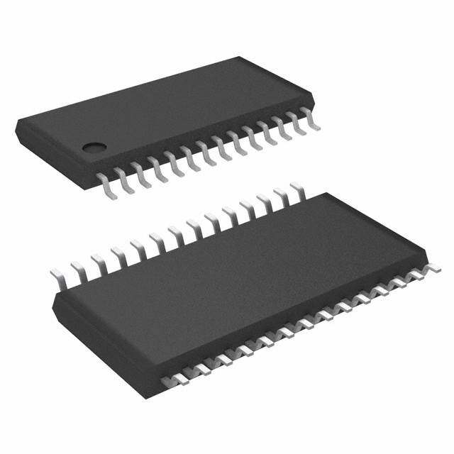
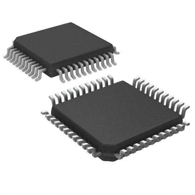
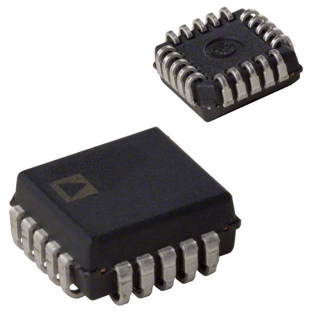
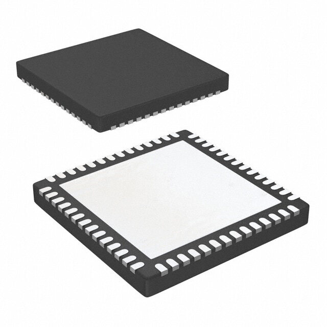
ICGOO在线商城 > 集成电路(IC) > 数据采集 - 模数转换器 > ADC0809CCV/NOPB
- 型号: ADC0809CCV/NOPB
- 制造商: Texas Instruments
- 库位|库存: xxxx|xxxx
- 要求:
| 数量阶梯 | 香港交货 | 国内含税 |
| +xxxx | $xxxx | ¥xxxx |
查看当月历史价格
查看今年历史价格
ADC0809CCV/NOPB产品简介:
ICGOO电子元器件商城为您提供ADC0809CCV/NOPB由Texas Instruments设计生产,在icgoo商城现货销售,并且可以通过原厂、代理商等渠道进行代购。 ADC0809CCV/NOPB价格参考。Texas InstrumentsADC0809CCV/NOPB封装/规格:数据采集 - 模数转换器, 8 Bit Analog to Digital Converter 8 Input 1 SAR 28-PLCC (11.51x11.51)。您可以下载ADC0809CCV/NOPB参考资料、Datasheet数据手册功能说明书,资料中有ADC0809CCV/NOPB 详细功能的应用电路图电压和使用方法及教程。
Texas Instruments的ADC0809CCV/NOPB是一款经典的8位模数转换器(ADC),广泛应用于各种数据采集系统中。它具有8个模拟输入通道,可以通过地址线选择其中一个通道进行转换,适用于多路信号采集的应用场景。以下是其主要应用场景:

1. 工业自动化:在工业控制系统中,ADC0809可以用于采集传感器数据,如温度、压力、湿度等物理量,并将其转换为数字信号,供微控制器或计算机处理。例如,在自动化生产线中,它可以实时监控环境参数,确保生产过程的稳定性和安全性。

2. 医疗设备:在医疗仪器中,ADC0809可用于将生物电信号(如心电图、脑电图等)转换为数字信号,以便进一步分析和诊断。它的低功耗和高可靠性使其非常适合便携式医疗设备。

3. 环境监测:在环境监测系统中,ADC0809可以连接多种传感器,如空气质量传感器、水质传感器等,实时采集环境数据并传输给中央控制系统,帮助环保部门及时掌握环境变化情况。

4. 智能家居:在智能家居系统中,ADC0809可以用于采集各种传感器数据,如温湿度、光照强度等,实现对家居环境的智能控制。例如,通过采集室内温度数据,自动调节空调或加热设备的工作状态。

5. 农业自动化:在现代农业中,ADC0809可以用于土壤湿度、光照强度等参数的采集,帮助农民优化灌溉和施肥方案,提高农作物产量和质量。

6. 汽车电子:在汽车电子系统中,ADC0809可以用于采集发动机温度、油压等关键参数,确保车辆运行的安全性和可靠性。它还可以用于车载娱乐系统的音频信号采集。

总之,ADC0809CCV/NOPB凭借其简单易用、性能稳定的特点,成为许多嵌入式系统和数据采集应用的理想选择。
| 参数 | 数值 |
| 产品目录 | 集成电路 (IC)半导体 |
| 描述 | IC ADC 8BIT MPU 8CH MUX 28-PLCC模数转换器 - ADC 8B MPU Compatible ADC |
| 产品分类 | |
| 品牌 | Texas Instruments |
| 产品手册 | |
| 产品图片 |
|
| rohs | 符合RoHS无铅 / 符合限制有害物质指令(RoHS)规范要求 |
| 产品系列 | 数据转换器IC,模数转换器 - ADC,Texas Instruments ADC0809CCV/NOPB- |
| 数据手册 | |
| 产品型号 | ADC0809CCV/NOPB |
| 产品 | ADC |
| 产品目录页面 | |
| 产品种类 | 模数转换器 - ADC |
| 位数 | 8 |
| 供应商器件封装 | 28-PLCC(11.51x11.51) |
| 信噪比 | Yes |
| 其它名称 | *ADC0809CCV/NOPB |
| 分辨率 | 8 bit |
| 包装 | 管件 |
| 商标 | Texas Instruments |
| 安装类型 | 表面贴装 |
| 安装风格 | SMD/SMT |
| 封装 | Tube |
| 封装/外壳 | 28-LCC(J 形引线) |
| 封装/箱体 | PLCC-28 |
| 工作温度 | -40°C ~ 85°C |
| 工作电源电压 | 5 V |
| 工厂包装数量 | 35 |
| 接口类型 | Parallel |
| 数据接口 | 并联 |
| 最大功率耗散 | 875 mW |
| 最大工作温度 | + 85 C |
| 最小工作温度 | - 40 C |
| 标准包装 | 35 |
| 电压参考 | External |
| 电压源 | 单电源 |
| 系列 | ADC0809-N |
| 结构 | SAR |
| 转换器数 | 1 |
| 转换器数量 | 1 |
| 转换速率 | 10 kS/s |
| 输入数和类型 | 8 个单端,单极 |
| 输入类型 | Single-Ended |
| 通道数量 | 8 Channel |
| 采样率(每秒) | 10k |


- 商务部:美国ITC正式对集成电路等产品启动337调查
- 曝三星4nm工艺存在良率问题 高通将骁龙8 Gen1或转产台积电
- 太阳诱电将投资9.5亿元在常州建新厂生产MLCC 预计2023年完工
- 英特尔发布欧洲新工厂建设计划 深化IDM 2.0 战略
- 台积电先进制程称霸业界 有大客户加持明年业绩稳了
- 达到5530亿美元!SIA预计今年全球半导体销售额将创下新高
- 英特尔拟将自动驾驶子公司Mobileye上市 估值或超500亿美元
- 三星加码芯片和SET,合并消费电子和移动部门,撤换高东真等 CEO
- 三星电子宣布重大人事变动 还合并消费电子和移动部门
- 海关总署:前11个月进口集成电路产品价值2.52万亿元 增长14.8%


PDF Datasheet 数据手册内容提取
ADC0808-N, ADC0809-N www.ti.com SNAS535H–OCTOBER1999–REVISEDMARCH2013 ADC0808/ADC0809 8-Bit μP Compatible A/D Converters with 8-Channel Multiplexer CheckforSamples:ADC0808-N,ADC0809-N FEATURES DESCRIPTION 1 • EasyInterfacetoAllMicroprocessors The ADC0808, ADC0809 data acquisition component 2 is a monolithic CMOS device with an 8-bit analog-to- • OperatesRatiometricallyorwith5V or DC digital converter, 8-channel multiplexer and AnalogSpanAdjustedVoltageReference microprocessor compatible control logic. The 8-bit • NoZeroorFull-ScaleAdjustRequired A/D converter uses successive approximation as the • 8-ChannelMultiplexerwithAddressLogic conversion technique. The converter features a high impedance chopper stabilized comparator, a 256R • 0VtoV InputRange CC voltage divider with analog switch tree and a • OutputsmeetTTLVoltageLevelSpecifications successive approximation register. The 8-channel • ADC0808EquivalenttoMM74C949 multiplexer can directly access any of 8-single-ended analogsignals. • ADC0809EquivalenttoMM74C949-1 The device eliminates the need for external zero and KEY SPECIFICATIONS full-scale adjustments. Easy interfacing to microprocessors is provided by the latched and • Resolution:8Bits decoded multiplexer address inputs and latched TTL • TotalUnadjustedError:±½LSBand ±1LSB TRI-STATEoutputs. • SingleSupply:5VDC The design of the ADC0808, ADC0809 has been • LowPower:15mW optimizedbyincorporatingthemostdesirableaspects of several A/D conversion techniques. The ADC0808, • ConversionTime:100μs ADC0809 offers high speed, high accuracy, minimal temperature dependence, excellent long-term accuracy and repeatability, and consumes minimal power. These features make this device ideally suited to applications from process and machine control to consumer and automotive applications. For 16- channelmultiplexerwithcommonoutput(sample/hold port) see ADC0816 data sheet. (See AN-247 (LiteratureNumberSNOA595)formoreinformation.) Block Diagram Connection Diagrams 1 Pleasebeawarethatanimportantnoticeconcerningavailability,standardwarranty,anduseincriticalapplicationsof TexasInstrumentssemiconductorproductsanddisclaimerstheretoappearsattheendofthisdatasheet. Alltrademarksarethepropertyoftheirrespectiveowners. 2 PRODUCTIONDATAinformationiscurrentasofpublicationdate. Copyright©1999–2013,TexasInstrumentsIncorporated Products conform to specifications per the terms of the Texas Instruments standard warranty. Production processing does not necessarilyincludetestingofallparameters.
ADC0808-N, ADC0809-N SNAS535H–OCTOBER1999–REVISEDMARCH2013 www.ti.com Figure1.PDIPPackage Figure2.PLCC SeePackageN0028E Package SeePackageFN0028A Thesedeviceshavelimitedbuilt-inESDprotection.Theleadsshouldbeshortedtogetherorthedeviceplacedinconductivefoam duringstorageorhandlingtopreventelectrostaticdamagetotheMOSgates. Absolute Maximum Ratings(1)(2)(3) SupplyVoltage(V )(4) 6.5V CC VoltageatAnyPinExceptControlInputs −0.3Vto(V +0.3V) CC VoltageatControlInputs −0.3Vto+15V (START,OE,CLOCK,ALE,ADDA,ADDB,ADDC) StorageTemperatureRange −65°Cto+150°C PackageDissipationatT =25°C 875mW A LeadTemp.(Soldering,10seconds) PDIPPackage(plastic) 260°C PLCCPackage VaporPhase(60seconds) 215°C Infrared(15seconds) 220°C ESDSusceptibility(5) 400V (1) AbsoluteMaximumRatingsindicatelimitsbeyondwhichdamagetothedevicemayoccur.DCandACelectricalspecificationsdonot applywhenoperatingthedevicebeyonditsspecifiedoperatingconditions. (2) AllvoltagesaremeasuredwithrespecttoGND,unlessotherwisespecified. (3) IfMilitary/Aerospacespecifieddevicesarerequired,pleasecontacttheTISalesOffice/Distributorsforavailabilityandspecifications. (4) AZenerdiodeexists,internally,fromV toGNDandhasatypicalbreakdownvoltageof7V . CC DC (5) Humanbodymodel,100pFdischargedthrougha1.5kΩresistor. Operating Conditions (1)(2) TemperatureRange T ≤T ≤T MIN A MAX −40°C≤T ≤+85°C A RangeofV 4.5V to6.0V CC DC DC (1) AbsoluteMaximumRatingsindicatelimitsbeyondwhichdamagetothedevicemayoccur.DCandACelectricalspecificationsdonot applywhenoperatingthedevicebeyonditsspecifiedoperatingconditions. (2) AllvoltagesaremeasuredwithrespecttoGND,unlessotherwisespecified. Electrical Characteristics – Converter Specifications ConverterSpecifications:V =5V =V ,V =GND,T ≤T ≤T andf =640kHzunlessotherwisestated. CC DC REF+ REF(−) MIN A MAX CLK Symbol Parameter Conditions Min Typ Max Units ADC0808 25°C ±½ LSB TotalUnadjustedError(1) T toT ±¾ LSB MIN MAX (1) Totalunadjustederrorincludesoffset,full-scale,linearity,andmultiplexererrors.SeeFigure5.NoneoftheseA/Dsrequiresazeroor full-scaleadjust.However,ifanallzerocodeisdesiredforananaloginputotherthan0.0V,orifanarrowfull-scalespanexists(for example:0.5Vto4.5Vfull-scale)thereferencevoltagescanbeadjustedtoachievethis.SeeFigure15. 2 SubmitDocumentationFeedback Copyright©1999–2013,TexasInstrumentsIncorporated ProductFolderLinks:ADC0808-N ADC0809-N
ADC0808-N, ADC0809-N www.ti.com SNAS535H–OCTOBER1999–REVISEDMARCH2013 Electrical Characteristics – Converter Specifications (continued) ConverterSpecifications:V =5V =V ,V =GND,T ≤T ≤T andf =640kHzunlessotherwisestated. CC DC REF+ REF(−) MIN A MAX CLK Symbol Parameter Conditions Min Typ Max Units ADC0809 0°Cto70°C ±1 LSB TotalUnadjustedError(1) T toT ±1¼ LSB MIN MAX InputResistance FromRef(+)toRef(−) 1.0 2.5 kΩ AnalogInputVoltageRange See (2)V(+)orV(−) GND−0.1 V +0.1 V CC DC V Voltage,TopofLadder MeasuredatRef(+) V V +0.1 V REF(+) CC CC Voltage,CenterofLadder (V /2)−0.1 V /2 (V /2)+0.1 V CC CC CC V Voltage,BottomofLadder MeasuredatRef(−) −0.1 0 V REF(−) I ComparatorInputCurrent f=640kHz,(3) −2 ±0.5 2 μA IN c (2) Twoon-chipdiodesaretiedtoeachanaloginputwhichwillforwardconductforanaloginputvoltagesonediodedropbelowgroundor onediodedropgreaterthantheV nsupply.Thespecallows100mVforwardbiasofeitherdiode.Thismeansthataslongasthe CC analogV doesnotexceedthesupplyvoltagebymorethan100mV,theoutputcodewillbecorrect.Toachieveanabsolute0V to IN DC 5V inputvoltagerangewillthereforerequireaminimumsupplyvoltageof4.900V overtemperaturevariations,initialtoleranceand DC DC loading. (3) Comparatorinputcurrentisabiascurrentintooroutofthechopperstabilizedcomparator.Thebiascurrentvariesdirectlywithclock frequencyandhaslittletemperaturedependence(Figure8).SeeANALOGCOMPARATORINPUTS Electrical Characteristics – Digital Levels and DC Specifications DigitalLevelsandDCSpecifications:ADC0808CCN,ADC0808CCV,ADC0809CCNandADC0809CCV,4.75≤V ≤5.25V, CC −40°C≤T ≤+85°Cunlessotherwisenoted A Symbol Parameter Conditions Min Typ Max Units ANALOGMULTIPLEXER V =5V,V =5V, CC IN I OFFChannelLeakageCurrent T =25°C 10 200 nA OFF(+) A T toT 1.0 μA MIN MAX V =5V,V =0, CC IN I OFFChannelLeakageCurrent T =25°C −200 −10 nA OFF(−) A T toT −1.0 μA MIN MAX CONTROLINPUTS V Logical“1”InputVoltage (V −1.5) V IN(1) CC V Logical“0”InputVoltage 1.5 V IN(0) Logical“1”InputCurrent(TheControl I V =15V 1.0 μA IN(1) Inputs) IN Logical“0”InputCurrent(TheControl I V =0 −1.0 μA IN(0) Inputs) IN I SupplyCurrent f =640kHz 0.3 3.0 mA CC CLK DATAOUTPUTSANDEOC(INTERRUPT) V =4.75V CC V Logical“1”OutputVoltage I =−360µA 2.4 V OUT(1) OUT I =−10µA 4.5 V OUT V Logical“0”OutputVoltage I =1.6mA 0.45 V OUT(0) O V Logical“0”OutputVoltageEOC I =1.2mA 0.45 V OUT(0) O V =5V 3 μA O I TRI-STATEOutputCurrent OUT V =0 −3 μA O Electrical Characteristics – Timing Specifications TimingSpecificationsV =V =5V,V =GND,t=t=20nsandT =25°Cunlessotherwisenoted. CC REF(+) REF(−) r f A Symbol Parameter Conditions MIn Typ Max Units t StartTimeDelayfromClock (Figure7) 300 900 ns STCLK Copyright©1999–2013,TexasInstrumentsIncorporated SubmitDocumentationFeedback 3 ProductFolderLinks:ADC0808-N ADC0809-N
ADC0808-N, ADC0809-N SNAS535H–OCTOBER1999–REVISEDMARCH2013 www.ti.com Electrical Characteristics – Timing Specifications (continued) TimingSpecificationsV =V =5V,V =GND,t=t=20nsandT =25°Cunlessotherwisenoted. CC REF(+) REF(−) r f A Symbol Parameter Conditions MIn Typ Max Units t MinimumStartPulseWidth (Figure7) 100 200 ns WS t MinimumALEPulseWidth (Figure7) 100 200 ns WALE t MinimumAddressSet-UpTime (Figure7) 25 50 ns s t MinimumAddressHoldTime (Figure7) 25 50 ns H t AnalogMUXDelayTimeFromALE R =0Ω(Figure7) 1 2.5 μs D S t ,t OEControltoQLogicState C =50pF,R =10k(Figure10) 125 250 ns H1 H0 L L t ,t OEControltoHi-Z C =10pF,R =10k(Figure10) 125 250 ns 1H 0H L L t ConversionTime f=640kHz,(Figure7)(1) 90 100 116 μs c c f ClockFrequency 10 640 1280 kHz c Clock t EOCDelayTime (Figure7) 0 8+2μS EOC Periods C InputCapacitance AtControlInputs 10 15 pF IN C TRI-STATEOutputCapacitance AtTRI-STATEOutputs 10 15 pF OUT (1) TheoutputsofthedataregisterareupdatedoneclockcyclebeforetherisingedgeofEOC. 4 SubmitDocumentationFeedback Copyright©1999–2013,TexasInstrumentsIncorporated ProductFolderLinks:ADC0808-N ADC0809-N
ADC0808-N, ADC0809-N www.ti.com SNAS535H–OCTOBER1999–REVISEDMARCH2013 Functional Description MULTIPLEXER The device contains an 8-channel single-ended analog signal multiplexer. A particular input channel is selected by using the address decoder. Table 1 shows the input states for the address lines to select any channel. The addressislatchedintothedecoderonthelow-to-hightransitionoftheaddresslatchenablesignal. Table1.AnalogChannelSelection SELECTEDANALOG ADDRESSLINE CHANNEL C B A IN0 L L L IN1 L L H IN2 L H L IN3 L H H IN4 H L L IN5 H L H IN6 H H L IN7 H H H CONVERTER CHARACTERISTICS TheConverter The heart of this single chip data acquisition system is its 8-bit analog-to-digital converter. The converter is designed to give fast, accurate, and repeatable conversions over a wide range of temperatures. The converter is partitioned into 3 major sections: the 256R ladder network, the successive approximation register, and the comparator.Theconverter'sdigitaloutputsarepositivetrue. The 256R ladder network approach (Figure 3) was chosen over the conventional R/2R ladder because of its inherent monotonicity, which ensures no missing digital codes. Monotonicity is particularly important in closed loop feedback control systems. A non-monotonic relationship can cause oscillations that will be catastrophic for thesystem.Additionally,the256Rnetworkdoesnotcauseloadvariationsonthereferencevoltage. The bottom resistor and the top resistor of the ladder network in Figure 3 are not the same value as the remainder of the network. The difference in these resistors causes the output characteristic to be symmetrical with the zero and full-scale points of the transfer curve. The first output transition occurs when the analog signal hasreached+½ LSBandsucceedingoutputtransitionsoccurevery1LSBlateruptofull-scale. The successive approximation register (SAR) performs 8 iterations to approximate the input voltage. For any SAR type converter, n-iterations are required for an n-bit converter. Figure 4 shows a typical example of a 3-bit converter. In the ADC0808, ADC0809, the approximation technique is extended to 8 bits using the 256R network. TheA/Dconverter'ssuccessiveapproximationregister(SAR)isresetonthepositiveedgeofthestartconversion start pulse. The conversion is begun on the falling edge of the start conversion pulse. A conversion in process will be interrupted by receipt of a new start conversion pulse. Continuous conversion may be accomplished by tyingtheend-of-conversion(EOC)outputtotheSCinput.Ifusedinthismode,anexternalstartconversionpulse should be applied after power up. End-of-conversion will go low between 0 and 8 clock pulses after the rising edgeofstartconversion. The most important section of the A/D converter is the comparator. It is this section which is responsible for the ultimate accuracy of the entire converter. It is also the comparator drift which has the greatest influence on the repeatability of the device. A chopper-stabilized comparator provides the most effective method of satisfying all theconverterrequirements. Thechopper-stabilizedcomparatorconvertstheDCinputsignalintoanACsignal.Thissignalisthenfedthrough a high gain AC amplifier and has the DC level restored. This technique limits the drift component of the amplifier since the drift is a DC component which is not passed by the AC amplifier. This makes the entire A/D converter extremelyinsensitivetotemperature,longtermdriftandinputoffseterrors. Copyright©1999–2013,TexasInstrumentsIncorporated SubmitDocumentationFeedback 5 ProductFolderLinks:ADC0808-N ADC0809-N
ADC0808-N, ADC0809-N SNAS535H–OCTOBER1999–REVISEDMARCH2013 www.ti.com Figure6showsatypicalerrorcurvefortheADC0808. Figure3. ResistorLadderandSwitchTree Figure4.3-BitA/DTransferCurve Figure5.3-BitA/DAbsoluteAccuracyCurve Figure6. TypicalErrorCurve 6 SubmitDocumentationFeedback Copyright©1999–2013,TexasInstrumentsIncorporated ProductFolderLinks:ADC0808-N ADC0809-N
ADC0808-N, ADC0809-N www.ti.com SNAS535H–OCTOBER1999–REVISEDMARCH2013 Timing Diagram Figure7. Copyright©1999–2013,TexasInstrumentsIncorporated SubmitDocumentationFeedback 7 ProductFolderLinks:ADC0808-N ADC0809-N
ADC0808-N, ADC0809-N SNAS535H–OCTOBER1999–REVISEDMARCH2013 www.ti.com Typical Performance Characteristics ComparatorI IN vs V IN (V =V =5V) CC REF Figure8. MultiplexerR ON vs V IN (V =V =5V) CC REF Figure9. 8 SubmitDocumentationFeedback Copyright©1999–2013,TexasInstrumentsIncorporated ProductFolderLinks:ADC0808-N ADC0809-N
ADC0808-N, ADC0809-N www.ti.com SNAS535H–OCTOBER1999–REVISEDMARCH2013 TRI-STATE Test Circuits and Timing Diagrams t ,t t ,t 1H H1 0H H0 t ,C =10pF t ,C =10pF 1H L 0H L t ,C =50pF t ,C =50pF H1 L H0 L tr tr 90% 90% 50% 50% 10% 10% tH1 tH0 50% 50% Figure10. TRI-STATETestCircuitsandTimingDiagrams Copyright©1999–2013,TexasInstrumentsIncorporated SubmitDocumentationFeedback 9 ProductFolderLinks:ADC0808-N ADC0809-N
ADC0808-N, ADC0809-N SNAS535H–OCTOBER1999–REVISEDMARCH2013 www.ti.com APPLICATIONS INFORMATION OPERATION RATIOMETRICCONVERSION The ADC0808, ADC0809 is designed as a complete Data Acquisition System (DAS) for ratiometric conversion systems. In ratiometric systems, the physical variable being measured is expressed as a percentage of full-scale which is not necessarily related to an absolute standard. The voltage input to the ADC0808 is expressed by the equation • V =InputvoltageintotheADC0808 IN • V =Full-scalevoltage fs • V =Zerovoltage Z • D =Datapointbeingmeasured X • D =Maximumdatalimit MAX • D =Minimumdatalimit (1) MIN A good example of a ratiometric transducer is a potentiometer used as a position sensor. The position of the wiper is directly proportional to the output voltage which is a ratio of the full-scale voltage across it. Since the data is represented as a proportion of full-scale, reference requirements are greatly reduced, eliminating a large source of error and cost for many applications. A major advantage of the ADC0808, ADC0809 is that the input voltage range is equal to the supply range so the transducers can be connected directly across the supply and theiroutputsconnecteddirectlyintothemultiplexerinputs,(Figure11). Ratiometric transducers such as potentiometers, strain gauges, thermistor bridges, pressure transducers, etc., are suitable for measuring proportional relationships; however, many types of measurements must be referred to an absolute standard such as voltage or current. This means a system reference must be used which relates the full-scale voltage to the standard volt. For example, if V =V =5.12V, then the full-scale range is divided into CC REF 256standardsteps.Thesmalleststandardstepis1LSBwhichisthen20mV. RESISTORLADDERLIMITATIONS The voltages from the resistor ladder are compared to the selected into 8 times in a conversion. These voltages are coupled to the comparator via an analog switch tree which is referenced to the supply. The voltages at the top,centerandbottomoftheladdermustbecontrolledtomaintainproperoperation. The top of the ladder, Ref(+), should not be more positive than the supply, and the bottom of the ladder, Ref(−), should not be more negative than ground. The center of the ladder voltage must also be near the center of the supply because the analog switch tree changes from N-channel switches to P-channel switches. These limitationsareautomaticallysatisfiedinratiometricsystemsandcanbeeasilymetingroundreferencedsystems. Figure 12 shows a ground referenced system with a separate supply and reference. In this system, the supply must be trimmed to match the reference voltage. For instance, if a 5.12V is used, the supply should be adjusted tothesamevoltagewithin0.1V. Figure11. RatiometricConversionSystem 10 SubmitDocumentationFeedback Copyright©1999–2013,TexasInstrumentsIncorporated ProductFolderLinks:ADC0808-N ADC0809-N
ADC0808-N, ADC0809-N www.ti.com SNAS535H–OCTOBER1999–REVISEDMARCH2013 The ADC0808 needs less than a milliamp of supply current so developing the supply from the reference is readily accomplished. In Figure 13 a ground referenced system is shown which generates the supply from the reference. The buffer shown can be an op amp of sufficient drive to supply the milliamp of supply current and the desired bus drive, or if a capacitive bus is driven by the outputs a large capacitor will supply the transient supply currentasseeninFigure14.TheLM301isovercompensatedtoinsurestabilitywhenloadedbythe10 μFoutput capacitor. The top and bottom ladder voltages cannot exceed V and ground, respectively, but they can be symmetrically CC less than V and greater than ground. The center of the ladder voltage should always be near the center of the CC supply. The sensitivity of the converter can be increased, (i.e., size of the LSB steps decreased) by using a symmetrical reference system. In Figure 15, a 2.5V reference is symmetrically centered about V /2 since the CC same current flows in identical resistors. This system with a 2.5V reference allows the LSB bit to be half the size ofa5Vreferencesystem. Figure12. GroundReferenced ConversionSystemUsingTrimmedSupply Figure13. GroundReferencedConversionSystemwith ReferenceGeneratingV Supply CC Copyright©1999–2013,TexasInstrumentsIncorporated SubmitDocumentationFeedback 11 ProductFolderLinks:ADC0808-N ADC0809-N
ADC0808-N, ADC0809-N SNAS535H–OCTOBER1999–REVISEDMARCH2013 www.ti.com Figure14. TypicalReferenceandSupplyCircuit R =R A B *Ratiometrictransducers Figure15. SymmetricallyCenteredReference CONVERTEREQUATIONS ThetransitionbetweenadjacentcodesNandN+1isgivenby: (2) ThecenterofanoutputcodeNisgivenby: (3) TheoutputcodeNforanarbitraryinputaretheintegerswithintherange: Where: • V =Voltageatcomparatorinput IN • V =VoltageatRef(+) REF(+) • V =VoltageatRef(−) REF(−) • V =Totalunadjustederrorvoltage(typically TUE • V ÷512) (4) REF(+) 12 SubmitDocumentationFeedback Copyright©1999–2013,TexasInstrumentsIncorporated ProductFolderLinks:ADC0808-N ADC0809-N
ADC0808-N, ADC0809-N www.ti.com SNAS535H–OCTOBER1999–REVISEDMARCH2013 ANALOGCOMPARATORINPUTS The dynamic comparator input current is caused by the periodic switching of on-chip stray capacitances. These are connected alternately to the output of the resistor ladder/switch tree network and to the comparator input as partoftheoperationofthechopperstabilizedcomparator. The average value of the comparator input current varies directly with clock frequency and with V as shown in IN Figure8. If no filter capacitors are used at the analog inputs and the signal source impedances are low, the comparator input current should not introduce converter errors, as the transient created by the capacitance discharge will die outbeforethecomparatoroutputisstrobed. If input filter capacitors are desired for noise reduction and signal conditioning they will tend to average out the dynamic comparator input current. It will then take on the characteristics of a DC bias current whose effect can bepredictedconventionally. Typical Application *Addresslatchesneededfor8085andSC/MPinterfacingtheADC0808toamicroprocessor Table2.MicroprocessorInterfaceTable PROCESSOR READ WRITE INTERRUPT(COMMENT) 8080 MEMR MEMW INTR(ThruRSTCircuit) 8085 RD WR INTR(ThruRSTCircuit) Z-80 RD WR INT(ThruRSTCircuit,Mode0) SC/MP NRDS NWDS SA(ThruSenseA) 6800 VMA•φ2•R/W VMA•φ•R/W IRQAorIRQB(ThruPIA) Copyright©1999–2013,TexasInstrumentsIncorporated SubmitDocumentationFeedback 13 ProductFolderLinks:ADC0808-N ADC0809-N
ADC0808-N, ADC0809-N SNAS535H–OCTOBER1999–REVISEDMARCH2013 www.ti.com REVISION HISTORY ChangesfromRevisionG(March2013)toRevisionH Page • ChangedlayoutofNationalDataSheettoTIformat.......................................................................................................... 13 14 SubmitDocumentationFeedback Copyright©1999–2013,TexasInstrumentsIncorporated ProductFolderLinks:ADC0808-N ADC0809-N
PACKAGE OPTION ADDENDUM www.ti.com 6-Feb-2020 PACKAGING INFORMATION Orderable Device Status Package Type Package Pins Package Eco Plan Lead/Ball Finish MSL Peak Temp Op Temp (°C) Device Marking Samples (1) Drawing Qty (2) (6) (3) (4/5) ADC0808CCV/NOPB ACTIVE PLCC FN 28 35 Green (RoHS SN Level-2A-245C-4 -40 to 85 ADC0808 & no Sb/Br) WEEK CCV ADC0808CCVX/NOPB ACTIVE PLCC FN 28 750 Green (RoHS SN Level-2A-245C-4 -40 to 85 ADC0808 & no Sb/Br) WEEK CCV ADC0809CCV/NOPB ACTIVE PLCC FN 28 35 Green (RoHS SN Level-2A-245C-4 -40 to 85 ADC0809 & no Sb/Br) WEEK CCV ADC0809CCVX/NOPB ACTIVE PLCC FN 28 750 Green (RoHS SN Level-2A-245C-4 -40 to 85 ADC0809 & no Sb/Br) WEEK CCV (1) The marketing status values are defined as follows: ACTIVE: Product device recommended for new designs. LIFEBUY: TI has announced that the device will be discontinued, and a lifetime-buy period is in effect. NRND: Not recommended for new designs. Device is in production to support existing customers, but TI does not recommend using this part in a new design. PREVIEW: Device has been announced but is not in production. Samples may or may not be available. OBSOLETE: TI has discontinued the production of the device. (2) RoHS: TI defines "RoHS" to mean semiconductor products that are compliant with the current EU RoHS requirements for all 10 RoHS substances, including the requirement that RoHS substance do not exceed 0.1% by weight in homogeneous materials. Where designed to be soldered at high temperatures, "RoHS" products are suitable for use in specified lead-free processes. TI may reference these types of products as "Pb-Free". RoHS Exempt: TI defines "RoHS Exempt" to mean products that contain lead but are compliant with EU RoHS pursuant to a specific EU RoHS exemption. Green: TI defines "Green" to mean the content of Chlorine (Cl) and Bromine (Br) based flame retardants meet JS709B low halogen requirements of <=1000ppm threshold. Antimony trioxide based flame retardants must also meet the <=1000ppm threshold requirement. (3) MSL, Peak Temp. - The Moisture Sensitivity Level rating according to the JEDEC industry standard classifications, and peak solder temperature. (4) There may be additional marking, which relates to the logo, the lot trace code information, or the environmental category on the device. (5) Multiple Device Markings will be inside parentheses. Only one Device Marking contained in parentheses and separated by a "~" will appear on a device. If a line is indented then it is a continuation of the previous line and the two combined represent the entire Device Marking for that device. (6) Lead/Ball Finish - Orderable Devices may have multiple material finish options. Finish options are separated by a vertical ruled line. Lead/Ball Finish values may wrap to two lines if the finish value exceeds the maximum column width. Important Information and Disclaimer:The information provided on this page represents TI's knowledge and belief as of the date that it is provided. TI bases its knowledge and belief on information provided by third parties, and makes no representation or warranty as to the accuracy of such information. Efforts are underway to better integrate information from third parties. TI has taken and Addendum-Page 1
PACKAGE OPTION ADDENDUM www.ti.com 6-Feb-2020 continues to take reasonable steps to provide representative and accurate information but may not have conducted destructive testing or chemical analysis on incoming materials and chemicals. TI and TI suppliers consider certain information to be proprietary, and thus CAS numbers and other limited information may not be available for release. In no event shall TI's liability arising out of such information exceed the total purchase price of the TI part(s) at issue in this document sold by TI to Customer on an annual basis. Addendum-Page 2
MECHANICAL DATA MPDI008 – OCTOBER 1994 N (R-PDIP-T**) PLASTIC DUAL-IN-LINE PACKAGE 24 PIN SHOWN A 24 13 0.560 (14,22) 0.520 (13,21) 1 12 0.060 (1,52) TYP 0.200 (5,08) MAX 0.610 (15,49) 0.020 (0,51) MIN 0.590 (14,99) Seating Plane 0.100 (2,54) 0.125 (3,18) MIN 0°–15° 0.021 (0,53) 0.010 (0,25) M 0.015 (0,38) 0.010 (0,25) NOM PINS ** 24 28 32 40 48 52 DIM 1.270 1.450 1.650 2.090 2.450 2.650 A MAX (32,26) (36,83) (41,91) (53,09) (62,23) (67,31) 1.230 1.410 1.610 2.040 2.390 2.590 A MIN (31,24) (35,81) (40,89) (51,82) (60,71) (65,79) 4040053/B 04/95 NOTES: A. All linear dimensions are in inches (millimeters). B. This drawing is subject to change without notice. C. Falls within JEDEC MS-011 D. Falls within JEDEC MS-015 (32 pin only) • POST OFFICE BOX 655303 DALLAS, TEXAS 75265
None
4215153/B 05/2017 PACKAGE OUTLINE FN0028A PLCC - 4.57 mm max height SCALE 1.000 PLASTIC CHIP CARRIER .180 MAX B .450-.456 [4.57] [11.43-11.58] .020 MIN NOTE 3 [0.51] A (.008) 4 1 28 [0.2] 5 25 PIN 1 ID .450-.456 (OPTIONAL) .382-.438 [11.43-11.58] [9.71-11.12] NOTE 3 11 19 12 18 .090-.120 TYP [2.29-3.04] 28X .026-.032 [0.66-0.81] C SEATING PLANE .004 [0.1] C 28X .013-.021 [0.33-0.53] 24X .050 .007 [0.18] C A B [1.27] .485-.495 [12.32-12.57] TYP 4215153/B 05/2017 NOTES: 1. All linear dimensions are in inches. Any dimensions in brackets are in millimeters. Any dimensions in parenthesis are for reference only. Controlling dimensions are in inches. Dimensioning and tolerancing per ASME Y14.5M. 2. This drawing is subject to change without notice. 3. Dimension does not include mold protrusion. Maximum allowable mold protrusion .01 in [0.25 mm] per side. 4. Reference JEDEC registration MS-018. www.ti.com
4215153/B 05/2017 EXAMPLE BOARD LAYOUT FN0028A PLCC - 4.57 mm max height PLASTIC CHIP CARRIER SYMM (R.002 ) TYP 28X (.094) 4 1 28 [0.05] [2.4] 28X (.026 ) [0.65] 5 25 SYMM (.429 ) 24X (.050 ) [10.9] [1.27] 11 19 12 18 (.429 ) [10.9] LAND PATTERN EXAMPLE EXPOSED METAL SHOWN SCALE:6X .002 MIN .002 MAX EXPOSED METAL EXPOSED METAL [0.05] [0.05] ALL AROUND ALL AROUND METAL SOLDER MASK SOLDER MASK METAL UNDER OPENING OPENING SOLDER MASK NON SOLDER MASK SOLDER MASK DEFINED DEFINED (PREFERRED) SOLDER MASK DETAILS 4215153/B 05/2017 NOTES: (continued) 5. Publication IPC-7351 may have alternate designs. 6. Solder mask tolerances between and around signal pads can vary based on board fabrication site. www.ti.com
EXAMPLE STENCIL DESIGN FFNN00002288AA PPLLCCCC -- 44..5577 mmmm mmaaxx hheeiigghhtt PPLLAASSTTIICC CCHHIIPP CCAARRRRIIEERR SYMM (R.002 ) TYP 28X (.094) 4 1 28 [0.05] [2.4] 28X (.026 ) [0.65] 5 25 SYMM (.429 ) 24X (.050 ) [10.9] [1.27] 11 19 12 18 (.429 ) [10.9] SOLDER PASTE EXAMPLE BASED ON 0.125 mm THICK STENCIL SCALE:6X 4215153/B 05/2017 NOTES: (continued) 7. Laser cutting apertures with trapezoidal walls and rounded corners may offer better paste release. IPC-7525 may have alternate design recommendations. 8. Board assembly site may have different recommendations for stencil design. www.ti.com
IMPORTANTNOTICEANDDISCLAIMER TI PROVIDES TECHNICAL AND RELIABILITY DATA (INCLUDING DATASHEETS), DESIGN RESOURCES (INCLUDING REFERENCE DESIGNS), APPLICATION OR OTHER DESIGN ADVICE, WEB TOOLS, SAFETY INFORMATION, AND OTHER RESOURCES “AS IS” AND WITH ALL FAULTS, AND DISCLAIMS ALL WARRANTIES, EXPRESS AND IMPLIED, INCLUDING WITHOUT LIMITATION ANY IMPLIED WARRANTIES OF MERCHANTABILITY, FITNESS FOR A PARTICULAR PURPOSE OR NON-INFRINGEMENT OF THIRD PARTY INTELLECTUAL PROPERTY RIGHTS. These resources are intended for skilled developers designing with TI products. You are solely responsible for (1) selecting the appropriate TI products for your application, (2) designing, validating and testing your application, and (3) ensuring your application meets applicable standards, and any other safety, security, or other requirements. These resources are subject to change without notice. TI grants you permission to use these resources only for development of an application that uses the TI products described in the resource. Other reproduction and display of these resources is prohibited. No license is granted to any other TI intellectual property right or to any third party intellectual property right. TI disclaims responsibility for, and you will fully indemnify TI and its representatives against, any claims, damages, costs, losses, and liabilities arising out of your use of these resources. TI’s products are provided subject to TI’s Terms of Sale (www.ti.com/legal/termsofsale.html) or other applicable terms available either on ti.com or provided in conjunction with such TI products. TI’s provision of these resources does not expand or otherwise alter TI’s applicable warranties or warranty disclaimers for TI products. Mailing Address: Texas Instruments, Post Office Box 655303, Dallas, Texas 75265 Copyright © 2020, Texas Instruments Incorporated
 Datasheet下载


