ICGOO在线商城 > 集成电路(IC) > 线性 - 放大器 - 仪表,运算放大器,缓冲器放大器 > ADA4940-2ACPZ-R7
 Datasheet下载
- 型号: ADA4940-2ACPZ-R7
- 制造商: Analog
- 库位|库存: xxxx|xxxx
- 要求:
| 数量阶梯 | 香港交货 | 国内含税 |
| +xxxx | $xxxx | ¥xxxx |
查看当月历史价格
查看今年历史价格
ADA4940-2ACPZ-R7产品简介:
ICGOO电子元器件商城为您提供ADA4940-2ACPZ-R7由Analog设计生产,在icgoo商城现货销售,并且可以通过原厂、代理商等渠道进行代购。 ADA4940-2ACPZ-R7价格参考¥32.00-¥38.40。AnalogADA4940-2ACPZ-R7封装/规格:线性 - 放大器 - 仪表,运算放大器,缓冲器放大器, Differential Amplifier 2 Circuit Differential 24-LFCSP-WQ (4x4)。您可以下载ADA4940-2ACPZ-R7参考资料、Datasheet数据手册功能说明书,资料中有ADA4940-2ACPZ-R7 详细功能的应用电路图电压和使用方法及教程。
ADA4940-2ACPZ-R7是Analog Devices Inc.推出的一款高性能、低功耗、全差分运算放大器,属于线性放大器类别中的差分放大器/缓冲器,常用于精密信号调理和高速数据采集系统。其典型应用场景包括:

1. 数据采集系统:适用于中高精度模数转换器(ADC)的驱动器,尤其在16位至24位Σ-Δ型或SAR型ADC前端电路中,提供低噪声、低失真的差分信号转换。

2. 工业测量与过程控制:用于传感器信号调理,如压力、温度、应变等微弱信号的放大与转换,满足工业自动化对高精度和稳定性的要求。

3. 医疗电子设备:在心电图(ECG)、脑电图(EEG)等生物电信号采集系统中,利用其低输入偏置电流和低噪声特性,实现对人体微弱生理信号的精确放大。

4. 便携式与电池供电设备:因其低功耗特性(每通道仅约1.5mA工作电流),适合用于手持仪器、无线传感器节点等对功耗敏感的应用。

5. 通信系统前端:可用于接收链路中的信号缓冲与驱动,支持宽带信号处理,具备良好的失真抑制能力。

6. 测试与测量仪器:在示波器、信号发生器、数字万用表等设备中,作为高保真信号路径的关键增益级或驱动级。

该器件采用紧凑的8引脚LFCSP封装(ACPZ),支持宽电源电压范围(3V至12V),具有出色的直流精度(低失调电压、低温漂)和交流性能(带宽达300MHz),可在-40°C至+125°C工业级温度范围内稳定工作,适用于高可靠性要求的环境。
| 参数 | 数值 |
| -3db带宽 | 260MHz |
| 产品目录 | 集成电路 (IC)半导体 |
| 描述 | IC OPAMP DIFF 260MHZ 24LFCSP差分放大器 Ultra Low Distortion Low Pwr ADC Dvr |
| 产品分类 | Linear - Amplifiers - Instrumentation, OP Amps, Buffer Amps集成电路 - IC |
| 品牌 | Analog Devices Inc |
| 产品手册 | |
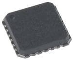
| 产品图片 |
|
| rohs | 符合RoHS无铅 / 符合限制有害物质指令(RoHS)规范要求 |
| 产品系列 | 放大器 IC,差分放大器,Analog Devices ADA4940-2ACPZ-R7- |
| 数据手册 | |
| 产品型号 | ADA4940-2ACPZ-R7 |
| PCN其它 | |
| 产品培训模块 | http://www.digikey.cn/PTM/IndividualPTM.page?site=cn&lang=zhs&ptm=25960http://www.digikey.cn/PTM/IndividualPTM.page?site=cn&lang=zhs&ptm=30008http://www.digikey.cn/PTM/IndividualPTM.page?site=cn&lang=zhs&ptm=26202 |
| 产品种类 | 差分放大器 |
| 供应商器件封装 | 24-LFCSP-VQ(4x4) |
| 共模抑制比—最小值 | 86 dB |
| 其它名称 | ADA4940-2ACPZ-R7DKR |
| 包装 | Digi-Reel® |
| 压摆率 | 95 V/µs |
| 可用增益调整 | 1 V/V |
| 商标 | Analog Devices |
| 增益带宽积 | - |
| 安装类型 | 表面贴装 |
| 安装风格 | SMD/SMT |
| 封装 | Reel |
| 封装/外壳 | 24-VFQFN 裸露焊盘,CSP |
| 封装/箱体 | LFCSP-24 |
| 工作温度 | -40°C ~ 125°C |
| 工作电源电压 | 3 V to 7 V |
| 工厂包装数量 | 1500 |
| 带宽 | 260 MHz |
| 放大器类型 | 差分 |
| 最大双重电源电压 | 7 V |
| 最大工作温度 | + 125 C |
| 最大输入电阻 | 50 MOhms |
| 最小工作温度 | - 40 C |
| 标准包装 | 1 |
| 特色产品 | http://www.digikey.com/product-highlights/cn/zh/analog-devices-ada4940-amplifiers/1876 |
| 电压-电源,单/双 (±) | 3 V ~ 7 V |
| 电压-输入失调 | 60µV |
| 电流-电源 | 1.25mA |
| 电流-输入偏置 | 1.1µA |
| 电流-输出/通道 | 46mA |
| 电源电流 | 1.25 mA |
| 电路数 | 2 |
| 稳定时间 | 34 ns |
| 系列 | ADA4940-2 |
| 视频文件 | http://www.digikey.cn/classic/video.aspx?PlayerID=1364138032001&width=640&height=505&videoID=2245193153001 |
| 转换速度 | 95 V/us |
| 输入补偿电压 | 0.06 mV |
| 输出类型 | 差分 |
| 通道数量 | 2 Channel |


- 商务部:美国ITC正式对集成电路等产品启动337调查
- 曝三星4nm工艺存在良率问题 高通将骁龙8 Gen1或转产台积电
- 太阳诱电将投资9.5亿元在常州建新厂生产MLCC 预计2023年完工
- 英特尔发布欧洲新工厂建设计划 深化IDM 2.0 战略
- 台积电先进制程称霸业界 有大客户加持明年业绩稳了
- 达到5530亿美元!SIA预计今年全球半导体销售额将创下新高
- 英特尔拟将自动驾驶子公司Mobileye上市 估值或超500亿美元
- 三星加码芯片和SET,合并消费电子和移动部门,撤换高东真等 CEO
- 三星电子宣布重大人事变动 还合并消费电子和移动部门
- 海关总署:前11个月进口集成电路产品价值2.52万亿元 增长14.8%


PDF Datasheet 数据手册内容提取
Ultralow Power, Low Distortion, Fully Differential ADC Drivers Data Sheet ADA4940-1/ADA4940-2 FEATURES FUNCTIONAL BLOCK DIAGRAMS ADA4940-1 Small signal bandwidth: 260 MHz S S S S V V V V Ultralow power 1.25mA – – – – 6 5 4 3 Extremely low harmonic distortion 1 1 1 1 −122 dB THD at 50 kHz –FB 1 12 DISABLE −96 dB THD at 1 MHz +IN 2 11 –OUT Low input voltage noise: 3.9 nV/√Hz –IN 3 10 +OUT 0.35 mV maximum offset voltage +FB 4 9 VOCM Balanced outputs Settling time to 0.1%: 34 ns 5 6 7 8 S S S S V V V V Rail-to-rail output: −V + 0.1 V to +V − 0.1 V + + + + S S AFldejxuibstlaeb ploe woeurt psuupt cpolimesm: 3o Vn- tmoo 7d Ve (vLoFlCtaSgPe) N1.O C–TVOESNS ONREC GTR TOHUEN EDX.POSED PAD TO 08452-001 Figure 1. ADA4940-1 Disable pin to reduce power consumption 1 E AADPAP4L9I4C0A-1T iIsO aNvaSi lable in LFCSP and SOIC packages N+1I –FB1–VS1–VS1 ABLDSI T1–OU 24 23 22 21 20 19 Low power PulSAR®/SAR ADC drivers –IN11 18+OUT1 Single-ended-to-differential conversion +FB12 17VOCM1 Differential buffers +VS13 16–VS2 ADA4940-2 Line drivers +VS14 15–VS2 Medical imaging –FB25 14DISABLE2 +IN26 13–OUT2 Industrial process controls Portable electronics 7 8 9 10 11 12 GENERAL DESCRIPTION –N2I +FB2+VS2+VS2 OCM2 OUT2 Tdihffee AreDntAia4l9 a4m0-p1li/fAieDrsA w49it4h0 v-2er ayr elo lwow p onwoiesre c, olonwsu dmisptotirotnio. nT fhuelyly N1.O C–TVOESNS ONREC GTR TOHUEN EDX.POSVED+ PAD TO 07429-202 Figure 2. ADA4940-2 are an ideal choice for driving low power, high resolution, high The ADA4940-1 is available in a 3 mm × 3 mm, 16-lead LFCSP performance SAR and Σ-Δ analog-to-digital converters (ADCs) and an 8-lead SOIC. The ADA4940-2 is available in a 4 mm × with resolutions up to 16 bits from dc to 1 MHz on only 1.25 mA 4 mm, 24-lead LFCSP. The pinouts are optimized to facilitate of quiescent current. The adjustable level of the output common- printed circuit board (PCB) layout and minimize distortion. mode voltage allows the ADA4940-1/ADA4940-2 to match the The ADA4940-1/ADA4940-2 are specified to operate over the input common-mode voltage of multiple ADCs. The internal −40°C to +125°C temperature range. common-mode feedback loop provides exceptional output balance, Table 1. Similar Products to ADA4940-1/ADA4940-2 as well as suppression of even-order harmonic distortion products. I Bandwidth Slew Rate Noise SUPPLY With the ADA4940-1/ADA4940-2, differential gain configurations Product (mA) (MHz) (V/μs) (nV/√Hz) are easily realized with a simple external feedback network of AD8137 3 110 450 8.25 four resistors determining the closed-loop gain of the amplifier. ADA4932-1 9 560 2800 3.6 The ADA4940-1/ADA4940-2 are fabricated using Analog Devices, ADA4941-1 2.2 31 22 5.1 Inc., SiGe complementary bipolar process, enabling them to Table 2. Complementary Products to ADA4940-1/ADA4940-2 achieve very low levels of distortion with an input voltage noise Power Throughput Resolution SNR of only 3.9 nV/√Hz. The low dc offset and excellent dynamic Product (mW) (MSPS) (Bits) (dB) performance of the ADA4940-1/ADA4940-2 make them well AD7982 7.0 1 18 98 suited for a variety of data acquisition and signal processing AD7984 10.5 1.333 18 96.5 applications. AD7621 65 3 16 88 AD7623 45 1.333 16 88 Rev. E Document Feedback Information furnished by Analog Devices is believed to be accurate and reliable. However, no responsibility is assumed by Analog Devices for its use, nor for any infringements of patents or other One Technology Way, P.O. Box 9106, Norwood, MA 02062-9106, U.S.A. rights of third parties that may result from its use. Specifications subject to change without notice. No license is granted by implication or otherwise under any patent or patent rights of Analog Devices. Tel: 781.329.4700 ©2011–2018 Analog Devices, Inc. All rights reserved. Trademarks and registered trademarks are the property of their respective owners. Technical Support www.analog.com
ADA4940-1/ADA4940-2 Data Sheet TABLE OF CONTENTS Features .............................................................................................. 1 Applications Information .............................................................. 23 Applications ....................................................................................... 1 Analyzing an Application Circuit ............................................ 23 General Description ......................................................................... 1 Setting the Closed-Loop Gain .................................................. 23 Functional Block Diagrams ............................................................. 1 Estimating the Output Noise Voltage ...................................... 23 Revision History ............................................................................... 3 Impact of Mismatches in the Feedback Networks ................. 24 Specifications ..................................................................................... 4 Calculating the Input Impedance of an Application Circuit 24 V = 5 V .......................................................................................... 4 Input Common-Mode Voltage Range ..................................... 25 S V = 3 V .......................................................................................... 6 Input and Output Capacitive AC Coupling ............................ 26 S Absolute Maximum Ratings ............................................................ 8 Setting the Output Common-Mode Voltage .......................... 26 Thermal Resistance ...................................................................... 8 DISABLE Pin .............................................................................. 26 Maximum Power Dissipation ..................................................... 8 Driving a Capacitive Load ......................................................... 26 ESD Caution .................................................................................. 8 Driving a High Precision ADC ................................................ 27 Pin Configurations and Function Descriptions ........................... 9 Layout, Grounding, and Bypassing .............................................. 28 Typical Performance Characteristics ........................................... 11 ADA4940-1 LFCSP Example .................................................... 28 Test Circuits ..................................................................................... 20 Outline Dimensions ....................................................................... 29 Terminology .................................................................................... 21 Ordering Guide .......................................................................... 30 Definition of Terms .................................................................... 21 Theory of Operation ...................................................................... 22 Rev. E | Page 2 of 30
Data Sheet ADA4940-1/ADA4940-2 REVISION HISTORY 4/2018—Rev. D to Rev. E Changes to Figure 37, Figure38, Figure 39, and Figure 41 ........ 15 Changes to Figure 2........................................................................... 1 Changes to Figure 49, Figure 50, and Figure 51 .......................... 17 Changes to Figure 6......................................................................... 10 Added Figure 55 and Figure 57 ..................................................... 18 Updated Outline Dimensions ........................................................ 29 Changes to Differential V , Differential CMRR, and V OS OCM CMRR Section ................................................................................. 20 5/2016—Rev. C to Rev. D Changes to Calculating the Input Impedance of an Application Changes to Figure 1........................................................................... 1 Circuit Section ................................................................................. 23 Deleted Figure 2................................................................................. 1 Changes to Figure 71 ...................................................................... 25 Added Figure 2; Renumbered Sequentially ................................... 1 Changes to Driving a High Precision ADC Section and Updated Outline Dimensions ........................................................ 29 Figure 73 ........................................................................................... 26 Changes to Ordering Guide ........................................................... 30 Changed ADA4940-1 Example Section to ADA4940-1 LFCSP Example Section .............................................................................. 27 9/2013—Rev. B to Rev. C Changes to Ordering Guide ........................................................... 29 Updated Outline Dimensions ........................................................ 30 Changes to Ordering Guide ........................................................... 31 12/2011—Rev. 0 to Rev. A Changes to Features Section, General Description Section, and 3/2012—Rev. A to Rev. B Table 1 ................................................................................................. 1 Reorganized Layout ........................................................... Universal Replaced Figure 1 and Figure 2 ....................................................... 1 Added ADA4940-1 8-Lead SOIC Package ..................... Universal Changes to V = ±2.5 V (or +5 V) Section and Table 3 ............... 3 S Changes to Features Section, Table 1, and Figure 1; Replaced Changes to Table 6 ............................................................................ 5 Figure 2 ............................................................................................... 1 Replaced Figure 7, Figure 8, Figure 9, and Figure 10 ................... 9 Changed V = ±2 V(or +5 V) Section to V = +5 V Section ....... 3 Replaced Figure 14, Figure 15, and Figure 17 ............................. 10 S S Changes to V = +5 V Section and Table 3 .................................... 3 Replaced Figure 24 and Figure 27 ................................................. 12 S Changes to Table 4 and Table 5 ....................................................... 4 Changes to Figure 37 ...................................................................... 14 Changes to V = 3 V Section and Table 6 ....................................... 5 Replaced Figure 43 and Figure 46 ................................................. 15 S Changes to Table 7 and Table 8 ....................................................... 6 Replaced Figure 53 .......................................................................... 18 Added Figure 5 and Table 12, Renumbered Sequentially ............ 9 Changes to Estimating the Output Noise Voltage Section, Table 14, Changes to Figure 7, Figure 8, and Figure 9 ................................ 10 Table 15, and Calculating the Input Impedance of an Application Added Figure 15 and Figure 18; Changes to Figure 13, Circuit Section ................................................................................. 21 Figure 14, and Figure 16 ................................................................. 11 Changes to Input Common-Mode Voltage Range Section ....... 22 Changes to Figure 19 and Figure 20 ............................................. 12 Changes to Driving a High Precision ADC Section and Changes to Figure 25, Figure 26, and Figure 27; Added Figure 65 ........................................................................................... 24 Figure 28, Figure 29, and Figure 30 .............................................. 13 Changes to Figure 31, Figure 32, Figure 33, Figure 34, Figure 35, 10/2011—Revision 0: Initial Version and Figure 36 ................................................................................... 14 Rev. E | Page 3 of 30
ADA4940-1/ADA4940-2 Data Sheet SPECIFICATIONS V = 5 V S V = midsupply, R = R = 1 kΩ, R = 1 kΩ, T = 25°C, LFCSP package, unless otherwise noted. T to T = −40°C to +125°C. OCM F G L, dm A MIN MAX (See Figure 61 for the definition of terms.) +D or –D to V Performance IN IN OUT, dm Table 3. Parameter Test Conditions/Comments Min Typ Max Unit DYNAMIC PERFORMANCE −3 dB Small Signal Bandwidth V = 0.1 V p-p, G = 1 260 MHz OUT, dm V = 0.1 V p-p, G = 2 220 MHz OUT, dm V = 0.1 V p-p, G = 5 75 MHz OUT, dm −3 dB Large Signal Bandwidth V = 2 V p-p, G = 1 25 MHz OUT, dm V = 2 V p-p, G = 2 22 MHz OUT, dm V = 2 V p-p, G = 5 19 MHz OUT, dm Bandwidth for 0.1 dB Flatness V = 2 V p-p, G = 1 and G = 2 14.5 MHz OUT, dm Slew Rate V = 2 V step 95 V/µs OUT, dm Settling Time to 0.1% V = 2 V step 34 ns OUT, dm Overdrive Recovery Time G = 2, V = 6 V p-p, triangle wave 86 ns IN, dm NOISE/HARMONIC PERFORMANCE HD2/HD3 V = 2 V p-p, f = 10 kHz −125/−118 dBc OUT, dm C V = 2 V p-p, f = 50 kHz −123/−126 dBc OUT, dm C V = 2 V p-p, f = 50 kHz, G = 2 −124/−117 dBc OUT, dm C V = 2 V p-p, f = 1 MHz −102/−96 dBc OUT, dm C V = 2 V p-p, f = 1 MHz, G = 2 −100/–92 dBc OUT, dm C IMD3 V = 2 V p-p, f = 1.9 MHz, f = 2.1 MHz −99 dBc OUT, dm 1 2 Input Voltage Noise f = 100 kHz 3.9 nV/√Hz Input Current Noise f = 100 kHz 0.81 pA/√Hz Crosstalk V = 2 V p-p, f = 1 MHz −110 dB OUT, dm C INPUT CHARACTERISTICS Input Offset Voltage V = V = V = 0 V −0.35 ±0.06 +0.35 mV IP IN OCM Input Offset Voltage Drift T to T 1.2 µV/°C MIN MAX Input Bias Current −1.6 −1.1 µA Input Bias Current Drift T to T −4.5 nA/°C MIN MAX Input Offset Current −500 ±50 +500 nA Input Common-Mode Voltage Range −V − 0.2 to V S +V − 1.2 S Input Resistance Differential 33 kΩ Common mode 50 MΩ Input Capacitance 1 pF Common-Mode Rejection Ratio (CMRR) ΔV /ΔV , ∆V = ±1 V dc 86 119 dB OS, dm IN, cm IN, cm Open-Loop Gain 91 99 dB OUTPUT CHARACTERISTICS Output Voltage Swing Each single-ended output −V + 0.1 to −V + 0.07 to V S S +V − 0.1 +V − 0.07 S S Linear Output Current f = 1 MHz, R = 22 Ω, SFDR = −60 dBc 46 mA peak L, dm Output Balance Error f = 1 MHz, ΔV /ΔV −65 −60 dB OUT, cm OUT, dm Rev. E | Page 4 of 30
Data Sheet ADA4940-1/ADA4940-2 V to V Performance OCM OUT, cm Table 4. Parameter Test Conditions/Comments Min Typ Max Unit V DYNAMIC PERFORMANCE OCM −3 dB Small Signal Bandwidth V = 0.1 V p-p 36 MHz OUT, cm −3 dB Large Signal Bandwidth V = 1 V p-p 29 MHz OUT, cm Slew Rate V = 1 V p-p 52 V/µs OUT, cm Input Voltage Noise f = 100 kHz 83 nV/√Hz Gain ΔV /ΔV , ΔV = ±1 V 0.99 1 1.01 V/V OUT, cm OCM OCM V CHARACTERISTICS OCM Input Common-Mode Voltage Range −V + 0.8 to V S +V − 0.7 S Input Resistance 250 kΩ Offset Voltage V = V − V ; V = V = V = 0 V −6 ±1 +6 mV OS, cm OUT, cm OCM IP IN OCM Input Offset Voltage Drift T to T 20 µV/°C MIN MAX Input Bias Current −7 +4 +7 µA CMRR ΔV /ΔV , ΔV = ±1 V 86 100 dB OS, dm OCM OCM General Performance Table 5. Parameter Test Conditions/Comments Min Typ Max Unit POWER SUPPLY Operating Range LFCSP 3 7 V SOIC 3 6 V Quiescent Current per Amplifier Enabled 1.05 1.25 1.38 mA Quiescent Current Drift T to T 4.25 µA/°C MIN MAX Disabled 13.5 28.5 µA +PSRR ΔV /ΔV, ΔV = 1 V p-p 80 90 dB OS, dm S S −PSRR ΔV /ΔV, ΔV = 1 V p-p 80 96 dB OS, dm S S DISABLE (DISABLE PIN) DISABLE Input Voltage Disabled ≤(−VS + 1) V Enabled ≥(−V + 1.8) V S Turn-Off Time 10 µs Turn-On Time 0.6 µs DISABLE Pin Bias Current per Amplifier Enabled DISABLE = +2.5 V 2 5 µA Disabled DISABLE = −2.5 V −10 −5 µA OPERATING TEMPERATURE RANGE −40 +125 °C Rev. E | Page 5 of 30
ADA4940-1/ADA4940-2 Data Sheet V = 3 V S V = midsupply, R = R = 1 kΩ, R = 1 kΩ, T = 25°C, LFCSP package, unless otherwise noted. T to T = −40°C to +125°C. OCM F G L, dm A MIN MAX (See Figure 61 for the definition of terms.) +D or –D to V Performance IN IN OUT, dm Table 6. Parameter Test Conditions/Comments Min Typ Max Unit DYNAMIC PERFORMANCE −3 dB Small Signal Bandwidth V = 0.1 V p-p 240 MHz OUT, dm V = 0.1 V p-p, G = 2 200 MHz OUT, dm V = 0.1 V p-p, G = 5 70 MHz OUT, dm −3 dB Large Signal Bandwidth V = 2 V p-p 24 MHz OUT, dm V = 2 V p-p, G = 2 20 MHz OUT, dm V = 2 V p-p, G = 5 17 MHz OUT, dm Bandwidth for 0.1 dB Flatness V = 0.1 V p-p 14 MHz OUT, dm Slew Rate V = 2 V step 90 V/µs OUT, dm Settling Time to 0.1% V = 2 V step 37 ns OUT, dm Overdrive Recovery Time G = 2, V = 3.6 V p-p, triangle wave 85 ns IN, dm NOISE/HARMONIC PERFORMANCE HD2/HD3 V = 2 V p-p, f = 50 kHz (HD2/HD3) −115/−121 dBc OUT, dm C V = 2 V p-p, f = 1 MHz (HD2/HD3) −104/−96 dBc OUT, dm C IMD3 V = 2 V p-p, f = 1.9 MHz, f = 2.1 MHz −98 dBc OUT, dm 1 2 Input Voltage Noise f = 100 kHz 3.9 nV/√Hz Input Current Noise f = 100 kHz 0.84 pA/√Hz Crosstalk V = 2 V p-p, f = 1 MHz −110 dB OUT, dm C INPUT CHARACTERISTICS Input Offset Voltage V = V = V = 1.5 V −0.4 ±0.06 +0.4 mV IP IN OCM Input Offset Voltage Drift T to T 1.2 µV/°C MIN MAX Input Bias Current −1.6 −1.1 µA Input Bias Current Drift T to T −4.5 nA/°C MIN MAX Input Offset Current −500 ±50 +500 nA Input Common-Mode Voltage Range −V − 0.2 to V S +V − 1.2 S Input Resistance Differential 33 kΩ Common mode 50 MΩ Input Capacitance 1 pF Common-Mode Rejection Ratio (CMRR) ΔV /ΔV , ∆V = ±0.25 V dc 86 114 dB OS, dm IN, cm IN, cm Open-Loop Gain 91 99 dB OUTPUT CHARACTERISTICS Output Voltage Swing Each single-ended output −V + 0.08 to −V + 0.04 to V S S +V − 0.08 +V − 0.04 S S Linear Output Current f = 1 MHz, R = 26 Ω, SFDR = −60 dBc 38 mA peak L, dm Output Balance Error f = 1 MHz, ΔV /ΔV −65 −60 dB OUT, cm OUT, dm Rev. E | Page 6 of 30
Data Sheet ADA4940-1/ADA4940-2 V to V Performance OCM OUT, cm Table 7. Parameter Test Conditions/Comments Min Typ Max Unit V DYNAMIC PERFORMANCE OCM −3 dB Small Signal Bandwidth V = 0.1 V p-p 36 MHz OUT, cm −3 dB Large Signal Bandwidth V = 1 V p-p 26 MHz OUT, cm Slew Rate V = 1 V p-p 48 V/µs OUT, cm Input Voltage Noise f = 100 kHz 92 nV/√Hz Gain ΔV /ΔV , ΔV = ±0.25 V 0.99 1 1.01 V/V OUT, cm OCM OCM V CHARACTERISTICS OCM Input Common-Mode Voltage Range −V + 0.8 to V S +V − 0.7 S Input Resistance 250 kΩ Offset Voltage V = V − V ; V = V = V = 1.5 V −7 ±1 +7 mV OS, cm OUT, cm OCM IP IN OCM Input Offset Voltage Drift T to T 20 µV/°C MIN MAX Input Bias Current −5 +1 +5 µA CMRR ΔV /ΔV , ΔV = ±0.25 V 80 100 dB OS,dm OCM OCM General Performance Table 8. Parameter Test Conditions/Comments Min Typ Max Unit POWER SUPPLY Operating Range LFCSP 3 7 V SOIC 3 6 V Quiescent Current per Amplifier Enabled 1 1.18 1.33 mA T to T 4.25 µA/°C MIN MAX Disabled 7 22 µA +PSRR ΔV /ΔV, ΔV = 0.25 V p-p 80 90 dB OS, dm S S −PSRR ΔV /ΔV, ΔV = 0.25 V p-p 80 96 dB OS, dm S S DISABLE (DISABLE PIN) DISABLE Input Voltage Disabled ≤(−VS + 1) V Enabled ≥(−V + 1.8) V S Turn-Off Time 16 µs Turn-On Time 0.6 µs DISABLE Pin Bias Current per Amplifier Enabled DISABLE = +3 V 0.3 1 µA Disabled DISABLE = 0 V −6 −3 µA OPERATING TEMPERATURE RANGE −40 +125 °C Rev. E | Page 7 of 30
ADA4940-1/ADA4940-2 Data Sheet ABSOLUTE MAXIMUM RATINGS The power dissipated in the package (P ) is the sum of the D Table 9. quiescent power dissipation and the power dissipated in the Parameter Rating package due to the load drive for all outputs. The quiescent Supply Voltage 8 V power dissipation is the voltage between the supply pins (±V) S V ±V OCM S times the quiescent current (I). The load current consists of the S Differential Input Voltage 1.2 V differential and common-mode currents flowing to the load, as Operating Temperature Range −40°C to +125°C well as currents flowing through the external feedback networks Storage Temperature Range −65°C to +150°C and internal common-mode feedback loop. The internal Lead Temperature (Soldering, 10 sec) 300°C resistor tap used in the common-mode feedback loop places a Junction Temperature 150°C negligible differential load on the output. Consider rms voltages ESD and currents when dealing with ac signals. Field Induced Charged Device Model (FICDM) 1250 V Airflow reduces θ . In addition, more metal directly in contact Human Body Model (HBM) 2000 V JA with the package leads from metal traces, through holes, ground, Stresses at or above those listed under Absolute Maximum and power planes reduces the θ . JA Ratings may cause permanent damage to the product. This is a Figure 3 shows the maximum safe power dissipation in the stress rating only; functional operation of the product at these package vs. the ambient temperature for the 8-lead SOIC (θ = JA or any other conditions above those indicated in the operational 158°C/W, single) the 16-lead LFCSP (θ = 91.3°C/W, single) JA section of this specification is not implied. Operation beyond and 24-lead LFCSP (θ = 65.1°C/W, dual) packages on a JEDEC JA the maximum operating conditions for extended periods may standard 4-layer board. θ values are approximations. JA affect product reliability. 3.5 THERMAL RESISTANCE θ is specified for the worst-case conditions, that is, θ is W) 3.0 spJAecified for the device soldered on a circuit board in JsAtill air. ON ( ADA4940-2 (LFCSP) TI 2.5 A P Table 10. SI ADA4940-1 (LFCSP) S 2.0 Package Type θJA Unit R DI E 8-Lead SOIC (Single)/4-Layer Board 158 °C/W W 1.5 O 16-Lead LFCSP (Single)/4-Layer Board 91.3 °C/W M P U 1.0 24-Lead LFCSP (Dual)/4-Layer Board 65.1 °C/W M XI MA 0.5 ADA4940-1 (SOIC) MAXIMUM POWER DISSIPATION TAhDeA m49a4x0im-2u pma cskaafeg epso iws elirm diitsesdip bayti othne i ans tshoec iAatDedA r4i9se4 0in-1 / 0–40 –20 0AMB2IE0NT TE4M0PERA60TURE 8(°0C) 100 120 08452-004 Figure 3. Maximum Safe Power Dissipation vs. Ambient Temperature junction temperature (T) on the die. At approximately 150°C, J which is the glass transition temperature, the plastic changes its properties. Even temporarily exceeding this temperature limit ESD CAUTION can change the stresses that the package exerts on the die, permanently shifting the parametric performance of the ADA4940-1/ADA4940-2. Exceeding a junction temperature of 150°C for an extended period can result in changes in the silicon devices, potentially causing failure. Rev. E | Page 8 of 30
Data Sheet ADA4940-1/ADA4940-2 PIN CONFIGURATIONS AND FUNCTION DESCRIPTIONS ADA4940-1 S S S S PIN 1 V V V V INDICATOR – – – – 6 5 4 3 1 1 1 1 –FB 1 12 DISABLE +IN 2 11 –OUT –IN 3 10 +OUT +FB 4 9 VOCM 5 6 7 8 S S S S V V V V + + + + N1.O C–TVOESNS ONREC GTR TOHUEN EDX.POSED PAD TO 08452-101 Figure 4. ADA4940-1 Pin Configuration (16-Lead LFCSP) Table 11. ADA4940-1 Pin Function Descriptions (16-Lead LFCSP) Pin No. Mnemonic Description 1 −FB Negative Output for Feedback Component Connection. 2 +IN Positive Input Summing Node. 3 −IN Negative Input Summing Node. 4 +FB Positive Output for Feedback Component Connection. 5 to 8 +V Positive Supply Voltage. S 9 V Output Common-Mode Voltage. OCM 10 +OUT Positive Output for Load Connection. 11 −OUT Negative Output for Load Connection. 12 DISABLE Disable Pin. 13 to 16 −V Negative Supply Voltage. S Exposed pad (EPAD) Connect the exposed pad to −V or ground. S –IN 1 8 +IN VOCM 2 7 DISABLE +O+UVTS 34 ADA4940-1 65 ––VOSUT 08452-003 Figure 5. ADA4940-1 Pin Configuration (8-Lead SOIC) Table 12. ADA4940-1 Pin Function Descriptions (8-Lead SOIC) Pin No. Mnemonic Description 1 −IN Negative Input Summing Node 2 V Output Common-Mode Voltage OCM 3 +V Positive Supply Voltage S 4 +OUT Positive Output for Load Connection 5 −OUT Negative Output for Load Connection 6 −V Negative Supply Voltage S 7 DISABLE Disable Pin 8 +IN Positive Input Summing Node Rev. E | Page 9 of 30
ADA4940-1/ADA4940-2 Data Sheet 1 E 1NI+ 1BF–V–1SV–1S LBASID 1TUO– 42 32 22 12 02 91 –IN11 18+OUT1 +FB12 17VOCM1 +VS13 16–VS2 ADA4940-2 +VS14 15–VS2 –FB25 14DISABLE2 +IN26 13–OUT2 7 8 9 01 11 21 2NI– 2BF+V+2SV+2S 2MCO 2TUO V + N1.O C–TVOESNS ONREC GTR TOHUEN EDX.POSED PAD TO 08452-102 Figure 6. ADA4940-2 Pin Configuration (24-Lead LFCSP) Table 13. ADA4940-2 Pin Function Descriptions (24-Lead LFCSP) Pin No. Mnemonic Description 1 −IN1 Negative Input Summing Node 1. 2 +FB1 Positive Output Feedback Pin 1. 3, 4 +V Positive Supply Voltage 1. S1 5 −FB2 Negative Output Feedback Pin 2. 6 +IN2 Positive Input Summing Node 2. 7 −IN2 Negative Input Summing Node 2. 8 +FB2 Positive Output Feedback Pin 2. 9, 10 +V Positive Supply Voltage 2. S2 11 V Output Common-Mode Voltage 2. OCM2 12 +OUT2 Positive Output 2. 13 −OUT2 Negative Output 2. 14 DISABLE2 Disable Pin 2. 15, 16 −V Negative Supply Voltage 2. S2 17 V Output Common-Mode Voltage 1. OCM1 18 +OUT1 Positive Output 1. 19 −OUT1 Negative Output 1. 20 DISABLE1 Disable Pin 1. 21, 22 −V Negative Supply Voltage 1. S1 23 −FB1 Negative Output Feedback Pin 1. 24 +IN1 Positive Input Summing Node 1. Exposed pad (EPAD) Connect the exposed pad to −V or ground. S Rev. E | Page 10 of 30
Data Sheet ADA4940-1/ADA4940-2 TYPICAL PERFORMANCE CHARACTERISTICS T = 25°C, V = ±2.5 V, G = 1, R = R = 1 kΩ, R = 52.3 Ω (when used), R = 1 kΩ, unless otherwise noted. See Figure 59 and Figure 60 for the A S F G T L test circuits. 3 3 2 G = 1, RL = 1kΩ 2 1 1 B) 0 B) 0 G = 2, RL = 1kΩ N (d –1 N (d –1 GAI –2 G = 1, RL = 200Ω GAI –2 ED –3 ED –3 Z Z ALI –4 G = 2, RL = 1kΩ ALI –4 RM –5 RM –5 G = 2, RL = 200Ω O O N –6 G = 2, RL = 200Ω N –6 –7 –7 G = 1, RL = 200Ω G = 1, RL = 1kΩ –8 VOUT, dm = 0.1V p-p –8 VOUT = 2V p-p –90.1 1 FREQUE1N0CY (MHz) 100 1000 08452-006 –90.1 1 FREQUE1N0CY (MHz) 100 1000 08452-009 Figure 7. Small Signal Frequency Response for Various Gains and Loads Figure 10. Large Signal Frequency Response for Various Gains and Loads (LFCSP) 3 3 VS = ±3.5V 2 2 1 1 VS = ±3.5V 0 0 VS = ±2.5V –1 –1 B) –2 B) –2 VS = ±2.5V AIN (d –3 VS = ±1.5V AIN (d –3 VS = ±1.5V G –4 G –4 –5 –5 –6 –6 –7 –7 –8 –8 –90.1VOUT, dm = 0.1V1 p-p FREQUE1N0CY (MHz) 100 1000 08452-007 –90.1VOUT = 2V p-p1 FREQUE1N0CY (MHz) 100 1000 08452-010 Figure 8. Small Signal Frequency Response for Various Supplies (LFCSP) Figure 11. Large Signal Frequency Response for Various Supplies 3 3 2 2 –40°C 1 1 0 0 –40°C –1 +25°C –1 +25°C B) –2 B) –2 N (d –3 N (d –3 +125°C AI +125°C AI G –4 G –4 –5 –5 –6 –6 –7 –7 –8 VOUT, dm = 0.1V p-p –8 VOUT, dm = 2V p-p –91 10FREQUENCY (MHz1)00 1000 08452-008 –91 10FREQUENCY (MHz1)00 1000 08452-011 Figure 9. Small Signal Frequency Response for Various Temperatures (LFCSP) Figure 12. Large Signal Frequency Response for Various Temperatures Rev. E | Page 11 of 30
ADA4940-1/ADA4940-2 Data Sheet 4 3 SOIC-1 LFCSP-1 3 LFCSP-1 2 LFCSP-2: CH1 2 1 LFCSP-2: CH2 SOIC-1 1 0 0 LFCSP-2: CH2 –1 –1 B) B) –2 N (d –2 LFCSP-2:CH1 N (d –3 AI –3 AI G G –4 –4 –5 –5 –6 –6 –7 –7 –8 VOUT, dm = 0.1V p-p –8 VOUT = 2V p-p –90.1 1 FREQUE1N0CY (MHz) 100 1000 08452-012 –91 10FREQUENCY (MHz1)00 1000 08452-015 Figure 13. Small Signal Frequency Response for Various Packages Figure 16. Large Signal Frequency Response for Various Packages 3 3 2 VOCM = 0V 2 VVOOCCMM == –01VV 1 1 VOCM = +1V 0 0 VOCM = –1V –1 –1 B) –2 B) –2 N (d –3 VOCM = +1V N (d –3 AI AI G –4 G –4 –5 –5 –6 –6 –7 –7 –8 VOUT, dm = 0.1V p-p –8 VOUT, dm = 2V p-p –90.1 1 FREQUE1N0CY (MHz) 100 1000 08452-013 –90.1 1 FREQUE1N0CY (MHz) 100 1000 08452-016 Figure 14. Small Signal Frequency Response at Various VOCM Levels (LFCSP) Figure 17. Large Signal Frequency Response at Various VOCM Levels 4 4 VOCM = 0V SOIC: RL = 1kΩ 3 3 SOIC: RL = 200Ω 2 2 1 1 0 0 B) –1 VOCM = –1V B) –1 LFCSP: RL = 1kΩ N (d –2 VOCM = +1V N (d –2 LFCSP: RL = 200Ω AI –3 AI –3 G G –4 –4 –5 –5 –6 –6 –7 –7 –8 VOUT, dm = 0.1V p-p –8 VOUT, dm = 0.1V p-p –90.1 1 FREQUE1N0CY (MHz) 100 1000 08452-205 –90.1 1 FREQUE1N0CY (MHz) 100 1000 08452-203 Figure 15. Small Signal Frequency Response for Various VOCM (SOIC) Figure 18. Small Signal Frequency Response for Various Packages and Loads Rev. E | Page 12 of 30
Data Sheet ADA4940-1/ADA4940-2 4 4 3 CCOM1 = CCOM2 = 2pF 3 CCOM1 = CCOM2 = 0pF CCOM1 = CCOM2 = 0.5pF 2 2 CCOM1 = CCOM2 = 1pF 1 1 CCOM1 = CCOM2 = 2pF 0 0 –1 CCOM1 = CCOM2 = 1pF –1 B) B) N (d –2 CCOM1 = CCOM2 = 0.5pF N (d –2 AI –3 CCOM1 = CCOM2 = 0pF AI –3 G G –4 –4 –5 –5 –6 –6 –7 –7 –8 CDIFF = 0pF –8 CDIFF = 0pF VOUT = 0.1V p-p VOUT = 2V p-p –91 10FREQUENCY (MHz1)00 1000 08452-014 –91 10FREQUENCY (MHz1)00 1000 08452-017 Figure 19. Small Signal Frequency Response for Various Capacitive Loads Figure 22. Large Signal Frequency Response for Various Capacitive Loads (LFCSP) 0.25 0.25 0.20 0.20 0.15 0.15 dB) 0.10 dB) 0.10 N ( N ( GAI 0.05 GAI 0.05 G = 1, RL = 1kΩ ED 0 ED 0 Z Z LI LI A–0.05 A–0.05 NORM–0.10 GG = = 2 ,2 ,R RL L= = 2 010kΩΩ NORM–0.10 G = 2, RL = 200Ω G = 2, RL = 1kΩ –0.15 G = 1, RL = 200Ω –0.15 G = 1, RL = 200Ω –0.20 –0.20 VOUT, dm = 0.1V p-p G = 1, RL = 1kΩ VOUT, dm = 2V p-p –0.250.1 1 FREQUE1N0CY (MHz) 100 1000 08452-018 –0.250.1 1 FREQUE1N0CY (MHz) 100 1000 08452-021 Figure 20. 0.1 dB Flatness Small Signal Frequency Response for Figure 23. 0.1 dB Flatness Large Signal Frequency Response for Various Gains and Loads (LFCSP) Various Gains and Loads 3 3 2 2 1 1 0 0 –1 VS = ±2.5V –1 VS = ±2.5V B) –2 B) –2 N (d –3 VS = ±1.5V N (d –3 VS = ±1.5V AI AI G –4 G –4 –5 –5 –6 –6 –7 –7 –8 VOUT, dm = 0.1V p-p –8 VOUT, dm = 1V p-p –91 10FREQUENCY (MHz1)00 1000 08452-019 –91 10FREQUENCY (MHz1)00 1000 08452-022 Figure 21. VOCM Small Signal Frequency Response for Various Supplies Figure 24. VOCM Large Signal Frequency Response for Various Supplies Rev. E | Page 13 of 30
ADA4940-1/ADA4940-2 Data Sheet –20 –20 –30 VOUT, dm = 2V p-p –30 VOUT, dm = 2V p-p HD3, G = 2 Bc) –40 Bc) –40 HD3, G = 1 N (d –50 N (d –50 RTIO –60 HD3, G = 2 RTIO –60 O –70 O –70 DIST –80 HD3, G = 1 DIST –80 C C NI –90 HD2, G = 2 NI –90 HD2, G = 2 O O RM –100 HD2, G = 1 RM –100 HD2, G = 1 A A H –110 H –110 –120 –120 –1300.01 0.1 FREQUENCY (M1Hz) 10 08452-023 –1300.01 0.1 FREQUENCY (M1Hz) 10 08452-200 Figure 25. Harmonic Distortion vs. Frequency for Various Gains (LFCSP) Figure 28. Harmonic Distortion vs. Frequency vs. Gain (SOIC) –20 –20 –30 VOUT, dm = 2V p-p –30 VOUT, dm = 2V p-p ORTION (dBc) ––––76540000 HD3, RL = 200Ω ORTION (dBc) ––––76540000 HD3, RL = 200Ω HARMONIC DIST ––11––10980000 HD2, RL H=D 13k,Ω RL = 1kΩ HD2, RL = 200Ω HARMONIC DIST ––11––10980000 HD2, RL = 1HkDΩ2, RL = 200Ω –120 –120 –1300.01 0.1 FREQUENCY (M1Hz) 10 08452-020 –1300.01 0.1 FHRDE3Q, URELN =C 1Yk Ω(M1Hz) 10 08452-201 Figure 26. Harmonic Distortion vs. Frequency for Various Loads (LFCSP) Figure 29. Harmonic Distortion vs. Frequency for Various Loads (SOIC) –20 –20 VOUT, dm = 2V p-p VOUT, dm = 2V p-p –30 –30 Bc) –40 Bc) –40 N (d –50 N (d –50 RTIO –60 RTIO –60 O –70 O –70 ST ST DI –80 DI –80 NIC –90 HD2, VS = ±3.5V NIC –90 O O ARM–100 HD2, VS = ±1.5HVD3, VS = ±1.5V ARM –100 HD2, ±2.5V H–110 HD3, VS = ±3.5V HD2, VS = ±2.5V H –110 HD2, ±1.5V –120 –120 HD3, VS = ±2.5V HD3, ±1.5V HD3, ±2.5V –1300.01 0.1 FREQUENCY (M1Hz) 10 08452-024 –1300.01 0.1 FREQUENCY (M1Hz) 10 08452-202 Figure 27. Harmonic Distortion vs. Frequency for Various Supplies (LFCSP) Figure 30. Harmonic Distortion vs. Frequency for Various Supplies (SOIC) Rev. E | Page 14 of 30
Data Sheet ADA4940-1/ADA4940-2 –20 –20 c) –30 VOUT, dm = 2V p-p –30 f = 1MHz VS = ±1.5V HD2 AMIC RANGE (dB ––––76540000 ORTION (dBc) ––––76540000 VS V=VS S± =1= . +5+3V3V VH,, D 00V3V HHDD23 DYN –80 DIST –80 VS = ±2.5V HD2 VS = ±3.5V HD2 REE –90 SOIC: RL = 200Ω NIC –90 RIOUS-F ––111000 SOIC: RL = 1kΩ HARMO––110100 VVSS == ±±32..55VV HHDD33 U –120 SP –120 LFCSP: RL = 1kΩ –130 –1300.01 0.1 FREQLUFECNSCPY: R(ML1H =z 2)00Ω 10 08452-030 –1400 1 2 3 V4OUT, dm5 (V p-6p) 7 8 9 10 08452-027 Figure 31. Spurious-Free Dynamic Range vs. Frequency at Figure 34. Harmonic Distortion vs. VOUT, dm for Various Supplies, f = 1 MHz RL = 200 Ω and RL = 1 kΩ (LFCSP) –20 –20 –30 VOUT, dm = 2V p-p –30 +VVOSU T=, d+m3V =, 2–VV Sp =-p 0V –40 –40 ON (dBc) ––6500 ON (dBc) ––6500 ORTI ––8700 HD3AT 1MHz ORTI –70 MONIC DIST ––11–109000 HD2AT 1MHz MONIC DIST –1––098000 HD2AT 1MHzHD3AT 1MHz AR –120 AR –110 H H HD2AT 100kHz –130 –120 HD3AT 100kHz –140 HD2AT 100kHz HD3AT 100kHz –130 –150–2.5 –2.0 –1.5 –1.0 –0.5VOC0M (V)0.5 1.0 1.5 2.0 2.5 08452-025 –1400 0.5 1.0 VOC1.M5 (V) 2.0 2.5 3.0 08452-028 Figure 32. Harmonic Distortion vs. VOCM for 100 kHz and 1 MHz, Figure 35. Harmonic Distortion vs. VOCM for 100 kHz and 1 MHz, 3 V Supply ±2.5 V Supplies (LFCSP) (LFCSP) –20 –20 –30 HD3AT VOUT, dm = 8V p-p –30 VOUT, dm = 2V p-p RTION (dBc) –––654000 HDHH2DDA23TAA VTTO VVUOOTUU, TTd,,m dd mm= 4==V 84 pVV- ppp--pp RTION (dBc) ––––76540000 O –70 O ST HD2AT VOUT, dm = 2V p-p ST –80 HD3, RF = RG = 499Ω DI –80 DI C C –90 NI –90 NI ARMO –100 HD3AT VOUT, dm = 2V p-p ARMO ––111000 HD2, RF = RG = 499Ω HD3, RF = RG = 1kΩ H H –110 –120 –120 –130 HD2, RF = RG = 1kΩ –1300.01 0.1 FREQUENCY (M1Hz) 10 08452-026 –1400.01 0.1 FREQUENCY (M1Hz) 10 08452-029 Figure 33. Harmonic Distortion vs. Frequency for Various VOUT, dm (LFCSP) Figure 36. Harmonic Distortion vs. Frequency for Various RF and RG (LFCSP) Rev. E | Page 15 of 30
ADA4940-1/ADA4940-2 Data Sheet 10 –60 0 V(EONUVTE, dLmO =P E2)V p-p VOUT, dm = 2V p-p –10 –70 c) B –20 d M ( –30 –80 CTRU –40 K (dB) –90 CHANNEL 1 TO CHANNEL 2 E –50 L P A S T MALIZED –––876000 CROSS ––111000 R O –90 CHANNEL 2 TO CHANNEL 1 N –100 –120 –110 –1201.5 1.6 1.7 1.8 FR1E.9QUE2N.0CY (M2.H1z) 2.2 2.3 2.4 2.5 08452-033 –1300.1 1 FREQUENCY (M1H0z) 100 08452-039 Figure 37. 2 MHz Intermodulation Distortion (LFCSP) Figure 40. Crosstalk vs. Frequency, ADA4940-2 130 120 120 110 100 110 LFCSP 90 100 B) B) 80 –PSRR R (d 90 R (d 70 R R M 80 S C SOIC P 60 +PSRR 70 50 60 40 50 30 400.1 1 FREQUENCY (M1H0z) 100 08452-100 200.1 1 FREQUENCY (M1H0z) 100 08452-034 Figure 38. CMRR vs. Frequency Figure 41. PSRR vs. Frequency –10 100 0 VOUT, dm = 2V p-p 90 –15 –20 80 –30 70 –45 B) –30 60 –60 d UT BALANCE ( ––5400 GAIN (dB) 23450000 ––––1197020550 ASE (Degrees) TP 10 –135 PH U O –60 0 –150 –10 –165 –70 –20 –180 –30 –195 –800.1 1 FREQUENCY (M1H0z) 100 08452-032 –4010k 100k F1RMEQUENCY 1(0HMz) 100M 1G–210 08452-035 Figure 39. Output Balance vs. Frequency Figure 42. Open-Loop Gain and Phase vs. Frequency Rev. E | Page 16 of 30
Data Sheet ADA4940-1/ADA4940-2 8 2.0 0.5 G = +2 1.6 0.4 6 VOUT, dm 1.2 INPUT 0.3 4 V) 0.8 0.2 E ( PUT VOLTAG –202 2 × VIN VOLTAGE (V) –00..440 OUTPUT %ERROR –000.1.1 ERROR (%) T U O –0.8 –0.2 –4 –1.2 –0.3 –6 –1.6 –0.4 VOUT, dm = 2V p-p –80 100 200 300 400TIM5E0 0(ns)600 700 800 900 1000 08452-041 –2.00 10 20 30 TIM4E0 (ns) 50 60 70 80–0.5 08452-065 Figure 43. Output Overdrive Recovery, G = 2 Figure 46. 0.1% Settling Time 100 100 Hz) √ 10 V/ Ω) E (n CE ( OIS AN N D T VOLTAGE 10 UTPUT IMPE 1 PU O 0.1 N I 110 100 1kFREQU1E0NkCY (Hz)100k 1M 10M 08452-037 0.010.1 1 FREQUENCY (M1H0z) 100 08452-040 Figure 44. Voltage Noise Spectral Density, Referred to Input Figure 47. Closed-Loop Output Impedance Magnitude vs. Frequency, G = 1 1.50 0 2.50 0 1.25 –OUT, VICM = 1V –0.25 2.25 R1 R2 –FB+D2I.S5AVBLE 0–V2.5V –0.25 1.00 –0.50 2.00 +IN –OUT DISABLE –0.50 OUTPUT VOLTAGE (V)––00000.....52257055050 DISABLE VICM RR011.1µFRR+–22IINN V–+OFFCBBM+–D22I..S55+–AVVOOBUULTTE 0–V2.5V ––––––211110......075207050505 DISABLE PIN VOLTAGE (V) OUTPUT VOLTAGE (V) 011110......025757050505 VICM R01.1µFR–2INV+OFCBM–2.5+VOUT –OUT, VICM = 1V ––––––211110......075207505050 DISABLE PIN VOLTAGE (V) –0.75 +OUT, VICM = 1V –2.25 0.25 +OUT, VICM = 1V –2.25 –1.00 –2.50 0 –2.50 –1.250 10 20 30 40TIM5E0 (µs)60 70 80 90 100–2.75 08452-038 –0.250 0.2 0.4 0.6 0.8TIM1E.0 (µs)1.2 1.4 1.6 1.8 2.0–2.75 08452-057 Figure 45. DISABLE Pin Turn-Off Time Figure 48. DISABLE Pin Turn-On Time Rev. E | Page 17 of 30
ADA4940-1/ADA4940-2 Data Sheet 100 1.5 G = 1, RL = 200Ω 80 G = 2, RL = 200Ω 1.0 60 OUTPUT VOLTAGE (mV) ––422400000 G =G 1 =, R2L, R=L 1 =k Ω1kΩ OUTPUT VOLTAGE (V) –00..550 GG == 11,, RRLL == 21k0Ω0Ω –60 –1.0 GG == 22,, RRLL == 12k0Ω0Ω –80 VOUT, dm = 0.1V p-p VOUT, dm = 2V p-p –1000 10 20 30 40 50 60TI7M0E 8(n0s)90 100110120130140150 08452-042 –1.50 20 40 60 80 100120T1IM40E1 (6n0s)180200220240260280300 08452-045 Figure 49. Small Signal Transient Response for Various Gains and Loads Figure 52. Large Signal Transient Response for Various Gains and Loads (LFCSP) 100 1.5 80 VS = ±3.5V VS = ±1.5V VS = ±1.5V 1.0 60 mV) 40 V) VS = ±2.5V OUTPUT VOLTAGE ( ––4220000 VS = ±2.5V OUTPUT VOLTAGE (–00..550 –60 –1.0 –80 VS = ±3.5V VOUT, dm= 0.1V VOUT, dm = 2V p-p –1000 10 20 30 40 50 60TI7M0E (8n0s)90 100110120130140150 08452-043 –1.50 20 40 60 80 100120T1IM40E 1(6n0s)180200220240260280300 08452-046 Figure 50. Small Signal Transient Response for Various Supplies (LFCSP) Figure 53. Large Signal Transient Response for Various Supplies 100 1.5 80 1.0 60 OUTPUT VOLTAGE (mV) ––422400000 CCCCCCCCOOOOMMMM1111 ==== CCCCCCCCOOOOMMMM2222 ==== 0012p.pp5FFFpF OUTPUT VOLTAGE (V) –00..550 CCCCCCCCOOOOMMMM1111 ==== CCCCCCCCOOOOMMMM2222 ==== 0012p.pp5FFFpF –60 –1.0 –80 CDIFF = 0pF CDIFF = 0pF VOUT, dm = 0.1V p-p VOUT, dm = 2V p-p –1000 10 20 30 40 50 60TI7M0E 8(n0s)90 100110120130140150 08452-044 –1.50 20 40 60 80 100120T1IM40E1 (6n0s)180200220240260280300 08452-047 Figure 51. Small Signal Transient Response for Various Capacitive Loads Figure 54. Large Signal Transient Response for Various Capacitive Loads (LFCSP) Rev. E | Page 18 of 30
Data Sheet ADA4940-1/ADA4940-2 100 100 LFCSP-1 LFCSP-1 80 LFCSP-2: CH1 80 LFCSP-2: CH1 LFCSP-2: CH2 LFCSP-2: CH2 SOIC-1 SOIC-1 60 60 V) V) m 40 m 40 E ( E ( G 20 G 20 A A T T OL 0 OL 0 V V UT –20 UT –20 P P T T U –40 U –40 O O –60 –60 –80 –80 VOUT, dm = 0.1V p-p VOUT, dm = 0.1V p-p –1000 10 20 30 40 50 60TI7M0E 8(n0s)90 100110120130140150 08452-204 –1000 10 20 30 40 50 60TI7M0E 8(n0s)90 100110120130140150 08452-206 Figure 55. Small Signal Transient Response for Various Packages, CL = 0 pF Figure 57. Small Signal Transient Response for Various Packages, CL = 2 pF 100 1.00 80 VS = ±2.5V 0.75 VS = ±2.5V 60 OUTPUT VOLTAGE (mV) ––422400000 VS = ±1.5V OUTPUT VOLTAGE (V)–000...2255500 VS = ±1.5V –0.50 –60 –0.75 –80 VOUT, dm = 0.1V p-p VOUT, dm = 1V p-p –1000 10 20 30 40 50 60TI7M0E 8(n0s)90 100110120130140150 08452-048 –1.000 20 40 60 80 100120T1IM40E1 (6n0s)180200220240260280300 08452-053 Figure 56. VOCM Small Signal Transient Response Figure 58. VOCM Large Signal Transient Response Rev. E | Page 19 of 30
ADA4940-1/ADA4940-2 Data Sheet TEST CIRCUITS 1kΩ NETWORK NETWORK ANALYZER +2.5V ANALYZER OUTPUT INPUT 50Ω 1kΩ 475Ω 50Ω VIN 52.3Ω VOCM ADA4940-1/ 54.9Ω ADA4940-2 1kΩ 54.9Ω 50Ω 25.5Ω 475Ω 1kΩ–2.5V 08452-067 Figure 59. Equivalent Basic Test Circuit 1kΩ DC-COUPLED +2.5V GENERATOR 100Ω 50Ω 50Ω LOW-PASS 1kΩ 475Ω 2:1 DUAL HP FILTER FILTER LP VIN 52.3Ω VOCM AADDAA44994400--12/ 54.9Ω CT 1kΩ 475Ω 54.9Ω 25.5Ω 1kΩ–2.5V 08452-056 Figure 60. Test Circuit for Distortion Measurements Rev. E | Page 20 of 30
Data Sheet ADA4940-1/ADA4940-2 TERMINOLOGY DEFINITION OF TERMS Common-Mode Offset Voltage The common-mode offset voltage is defined as the difference –FB between the voltage applied to the V terminal and the RF OCM common mode of the output voltage. +DIN RG +IN –OUT – VOS, cm = VOUT, cm − VOCM +VOCM AADDAA44994400--12/ RVOL,U dTm, dm Differential VOS, Differential CMRR, and VOCM CMRR + –DIN RG –IN +OUT The differential mode and common-mode voltages each have their own error sources. The differential offset (V ) is the RF +FB 08452-090 vDoilftfaegree nertiraolr CbMetwReRe nr etfhlee c+tsIN th aen cdh −aInNge t eorfm VinOSa, ldsm o ifn Ot Shr, eedms apmonplsiefi etor. Figure 61. Circuit Definitions changes to the common-mode voltage at the input terminals Differential Voltage +DIN and −DIN. Differential voltage refers to the difference between two node CMRR ΔVIN,cm voltages. For example, the differential output voltage (or DIFF ΔV OS,dm equivalently, output differential mode voltage) is defined as V CMRR reflects the change of V in response to OCM OS, dm V = (V − V ) OUT, dm +OUT −OUT changes to the common-mode voltage at the output terminals. where V and V refer to the voltages at the +OUT and −OUT te+rOmUTinals w−iOthUT respect to a common reference. CMRR ΔVOCM VOCM ΔV Similarly, the differential input voltage is defined as OS,dm Balance V = (+D − (−D )) IN, dm IN IN Balance is a measure of how well the differential signals are Common-Mode Voltage (CMV) matched in amplitude; the differential signals are exactly 180° CMV refers to the average of two node voltages. The output apart in phase. By this definition, the output balance is the common-mode voltage is defined as magnitude of the output common-mode voltage divided by V = (V + V )/2 the magnitude of the output differential mode voltage. OUT, cm +OUT −OUT Similarly, the input common-mode voltage is defined as V OutputBalanceError OUT,cm VIN, cm = (+DIN + (−DIN))/2 V OUT,dm Rev. E | Page 21 of 30
ADA4940-1/ADA4940-2 Data Sheet THEORY OF OPERATION The differential feedback loop forces the voltages at +IN and −IN The ADA4940-1/ADA4940-2 are high speed, low power to equal each other. This fact sets the following relationships: differential amplifiers fabricated on Analog Devices advanced dielectrically isolated SiGe bipolar process. They provide two +D V IN =− −OUT closely balanced differential outputs in response to either R R G F differential or single-ended input signals. An external feedback −D V network that is similar to a voltage feedback operational IN =− +OUT amplifier sets the differential gain. The output common-mode RG RF voltage is independent of the input common-mode voltage and Subtracting the previous equations gives the relationship that is set by an external voltage at the V terminal. The PNP OCM shows R and R setting the differential gain. F G input stage allows input common-mode voltages between the R negative supply and 1.2 V below the positive supply. A rail-to- (V − V ) = (+D – (−D )) × F +OUT −OUT IN IN R rail output stage supplies a wide output voltage range. G The DISABLE pin can reduce the supply current of the The common-mode feedback loop drives the output common- amplifier to 13.5 µA. mode voltage that is sampled at the midpoint of the output Figure 62 shows the ADA4940-1/ADA4940-2 architecture. voltage divider to equal the voltage at VOCM. This results in the The differential feedback loop consists of the differential trans- following relationships: conductance GDIFF working through the GO output buffers and V+OUT = VOCM + VOUT,dm the RF/RG feedback networks. The common-mode feedback 2 loop is set up with a voltage divider across the two differential V−OUT = VOCM − VOUT,dm outputs to create an output voltage midpoint and a common- 2 mode transconductance, G . CM Note that the differential amplifier’s summing junction input RG RF voltages, +IN and −IN, are set by both the output voltages and +DIN CC the input voltages. R R V =+D F +V G +IN INR +R −OUTR +R GO –OUT F G F G R R +IN GDIFF GCM V−IN =−DINRF +FRG+V+OUTRF +GRG –IN VOCM VREF GO +OUT –DIN RG CC RF 08452-058 Figure 62. ADA4940-1/ADA4940-2 Architectural Block Rev. E | Page 22 of 30
Data Sheet ADA4940-1/ADA4940-2 APPLICATIONS INFORMATION ANALYZING AN APPLICATION CIRCUIT VnRG1 RG1 RF1 VnRF1 The ADA4940-1/ADA4940-2 use open-loop gain and negative inIN+ feedback to force their differential and common-mode output + voltages in such a way as to minimize the differential and common- mode error voltages. The differential error voltage is defined as inIN– VnIN AADDAA44994400--12/ VnOD the voltage between the differential inputs labeled +IN and −IN (see Figure 61). For most purposes, this voltage is zero. Similarly, the difference between the actual output common-mode voltage and VOCM tahsesu vmolptatgioe nasp,p alnieyd atpop VliOcCaMti iosn a lcsior czueirto c. aSnta brtei nagn afrlyozmed t.h ese two VnRG2 RG2 RF2 VnRF2 VnCM 08452-050 Figure 63. ADA4940-1/ADA4940-2 Noise Model SETTING THE CLOSED-LOOP GAIN As with conventional op amp, the output noise voltage densities Determine the differential mode gain of the circuit in Figure 61 can be estimated by multiplying the input-referred terms at +IN by using the following equation: and −IN by the appropriate output factor, VOUT,dm = RF where: V R 2 IN,dm G G = is the circuit noise gain. N (β +β ) This assumes that the input resistors (R ) and feedback resistors 1 2 G R R (RF) on each side are equal. β1= R +G1R and β2 = R +G2R are the feedback factors. ESTIMATING THE OUTPUT NOISE VOLTAGE F1 G1 F2 G2 When R /R = R /R , then β1 = β2 = β, and the noise gain F1 G1 F2 G2 Estimate the differential output noise of the ADA4940-1/ becomes ADA4940-2 by using the noise model in Figure 63. The input- referred noise voltage density, vnIN, is modeled as a differential G = 1 =1+ RF input, and the noise currents, i and i , appear between N β R nIN− nIN+ G each input and ground. The noise currents are assumed equal Note that the output noise from V goes to zero in this case. OCM and produce a voltage across the parallel combination of the gain The total differential output noise density, v , is the root-sum- nOD and feedback resistances. v is the noise voltage density at the nCM square of the individual output noise terms. V pin. Each of the four resistors contributes (4kTR)1/2. Table 14 OCM x summarizes the input noise sources, the multiplication factors, 8 v = ∑v2 and the output-referred noise density terms. For more noise nOD nOi i=1 calculation information, go to the Analog Devices Differential Amplifier Calculator (DiffAmpCalc™), click ADIDiffAmpCalculator.zip, and follow the on-screen prompts. Table 14. Output Noise Voltage Density Calculations Input Noise Output Output-Referred Noise Input Noise Contribution Input Noise Term Voltage Density Multiplication Factor Voltage Density Term Differential Input v v G v = G (v ) nIN nIN N nO1 N nIN Inverting Input i i × (R ||R ) G v = G [i × (R ||R )] nIN− nIN− G2 F2 N nO2 N nIN− G2 F2 Noninverting Input i i × (R ||R ) G v = G [i × (R ||R )] nIN+ nIN+ G1 F1 N nO3 N nIN+ G1 F1 V Input v v G (β − β) v = G (β − β)(v ) OCM nCM nCM N 1 2 nO4 N 1 2 nCM Gain Resistor R v (4kTR )1/2 G (1 − β) v = G (1 − β)(4kTR )1/2 G1 nRG1 G1 N 2 nO5 N 2 G1 Gain Resistor R v (4kTR )1/2 G (1 − β) v = G (1 − β)(4kTR )1/2 G2 nRG2 G2 N 1 nO6 N 1 G2 Feedback Resistor R v (4kTR )1/2 1 v = (4kTR )1/2 F1 nRF1 F1 nO7 F1 Feedback Resistor R v (4kTR )1/2 1 v = (4kTR )1/2 F2 nRF2 F2 nO8 F2 Rev. E | Page 23 of 30
ADA4940-1/ADA4940-2 Data Sheet Table 15 and Table 16 list several common gain settings, recommended resistor values, input impedances, and output noise density for both balanced and unbalanced input configurations. Table 15. Differential Ground-Referenced Input, DC-Coupled, R = 1 kΩ (See Figure 64) L Nominal Gain (dB) R (Ω) R (Ω) R (Ω) Differential Output Noise Density (nV/√Hz) RTI (nV/√Hz) F G IN, dm 0 1000 1000 2000 11.3 11.3 6 1000 500 1000 15.4 7.7 10 1000 318 636 20.0 6.8 14 1000 196 392 27.7 5.5 Table 16. Single-Ended Ground-Referenced Input, DC-Coupled, R = 50 Ω, R = 1 kΩ (See Figure 65) S L Nominal Gain (dB) R (Ω) R (Ω) R (Ω) R (Ω) R (Ω)1 Differential Output Noise Density (nV/√Hz) RTI (nV/√Hz) F G T IN, se G1 0 1000 1000 52.3 1333 1025 11.2 11.2 6 1000 500 53.6 750 526 15.0 7.5 10 1000 318 54.9 512 344 19.0 6.3 14 1000 196 59.0 337 223 25.3 5 1 RG1 = RG + (RS||RT) IMPACT OF MISMATCHES IN THE FEEDBACK For an unbalanced, single-ended input signal (see Figure 65), NETWORKS the input impedance is Even if the external feedback networks (RF/RG) are mismatched, the internal common-mode feedback loop still forces the outputs R = RG IN,se R troem reamina ienq buaalla anncded 1. 8T0h°e o aumt polfi tpuhdaesse o. fT thhee siingpnuatl-st aot- eoaucthp uotu,t put 1−2×(RGF+RF) differential mode gain varies proportionately to the feedback RF mismatch, but the output balance is unaffected. +VS As well as causing a noise contribution from V , ratio-matching OCM RG +IN errors in the external resistors result in a degradation of the ability +DIN VOCM ADA4940-1/ of the circuit to reject input common-mode signals, much the ADA4940-2 VOUT, dm same as for a four resistors difference amplifier made from a –DIN RG –IN conventional op amp. In addition, if the dc levels of the input and output common- RF 08452-051 mode voltages are different, matching errors result in a small Figure 64. ADA4940-1/ADA4940-2 Configured for Balanced (Differential) Inputs differential mode, output offset voltage. When G = 1, with a RF ground-referenced input signal and the output common-mode +VS level set to 2.5 V, an output offset of as much as 25 mV (1% of RS RG +IN the difference in common-mode levels) can result if 1% tolerance resistors are used. Resistors of 1% tolerance result in a worst- RT VOCM AADDAA44994400--12/ VOUT, dm case input CMRR of about 40 dB, a worst-case differential mode RG output offset of 25 mV due to the 2.5 V level-shift, and no –IN significant degradation in output balance error. RS RT RF 08452-052 CALCULATING THE INPUT IMPEDANCE OF AN Figure 65. ADA4940-1/ADA4940-2 Configured for APPLICATION CIRCUIT Unbalanced (Single-Ended) Input The effective input impedance of a circuit depends on whether The input impedance of the circuit is effectively higher than it the amplifier is being driven by a single-ended or differential would be for a conventional op amp connected as an inverter signal source. For balanced differential input signals, as shown because a fraction of the differential output voltage appears at in Figure 64, the input impedance (R ) between the inputs the inputs as a common-mode signal, partially bootstrapping IN, dm (+DIN and −DIN) is simply RIN, dm = 2 × RG. the voltage across the input resistor RG1. Rev. E | Page 24 of 30
Data Sheet ADA4940-1/ADA4940-2 Terminating a Single-Ended Input RS RTH 50Ω RT 25.5Ω This section describes how to properly terminate a single-ended VS 52.3Ω VTH iannpdu Rt Gto = t h1 ek AΩD. AAn4 e9x4a0m-1p/lAe uDsAin4g9 a4n0 i-n2p wuti tsho ua rgcaei nw iotfh 1 a, tReFr m= i1n aktΩed 2V p-p 1.02V p-p 08452-061 output voltage of 1 V p-p and source resistance of 50 Ω illustrates Figure 68. Calculating the Thevenin Equivalent the three steps that must be followed. Because the terminated R = R = R||R = 25.5 Ω. Note that V is greater than TS TH S T TH output voltage of the source is 1 V p-p, the open-circuit output 1 V p-p, which was obtained with R = 50 Ω. The modified T voltage of the source is 2 V p-p. The source shown in Figure 66 circuit with the Thevenin equivalent (closest 1% value used for indicates this open-circuit voltage. R ) of the terminated source and R in the lower feedback TH TS RF loop is shown in Figure 69. RIN, se 1kΩ RF 1.33kΩ +VS 1kΩ RS RG +VS 2V pV-pS 50Ω V1OkΩCM AADDAA44994400--12 RL VOUT, dm 2R5.T5HΩ 1RkGΩ RG 1.02V VpT-pH VOCM AADDAA44994400--12 RL VOUT, dm 1kΩ RG –VS 25R.5TΩS 1kΩ Figure 66. Calculating Single-E1nRkdFΩed Input Impedance, RIN 08452-059 1RkFΩ–VS 08452-062 1. The input impedance is calculated by Figure 69. Thevenin Equivalent and Matched Gain Resistors Figure 69 presents a tractable circuit with matched feedback loops that can be easily evaluated. R = RG = 1000 = 1.33kΩ IN,se 1− RF 1− 1000 It is useful to point out two effects that occur with a terminated 2×(RG+RF) 2×(1000 + 1000) input. The first is that the value of RG is increased in both loops, lowering the overall closed-loop gain. The second is that V 2. To match the 50 Ω source resistance, calculate the TH is a little larger than 1 V p-p, as it would be if R = 50 Ω. termination resistor, R , using R ||1.33 kΩ = 50 Ω. T T T These two effects have opposite impacts on the output voltage, The closest standard 1% value for R is 52.3 Ω. T and for large resistor values in the feedback loops (~1 kΩ), the RF effects essentially cancel each other out. For small R and R , F G RIN, se 1kΩ or high gains, however, the diminished closed-loop gain is not 50Ω +VS cancelled completely by the increased V . This can be seen by TH RS RG evaluating Figure 69. 2V pV-pS 50Ω 52.3RΩT V1OkΩCM AADDAA44994400--12 RL VOUT, dm The desired differential output in this example is 1 V p-p RG because the terminated input signal was 1 V p-p and the 1kΩ closed-loop gain = 1. The actual differential output voltage, however, is equal to (1.02 V p-p)(1000/1025.5) = 0.996 V p-p. –VS This is within the tolerance of the resistors, so no change to 1RkFΩ 08452-060 the feedback resistor, RF, is required. Figure 67. Adding Termination Resistor RT INPUT COMMON-MODE VOLTAGE RANGE 3. Figure 67 shows that the effective R in the upper feedback G The ADA4940-1/ADA4940-2 input common-mode range is loop is now greater than the R in the lower loop due to the G shifted down by approximately 1 V , in contrast to other ADC BE addition of the termination resistors. To compensate for the drivers with centered input ranges, such as the ADA4939-1/ imbalance of the gain resistors, add a correction resistor (R ) TS ADA4939-2. The downward-shifted input common-mode range in series with R in the lower loop. R is the Thevenin G TS is especially suited to dc-coupled, single-ended-to-differential, equivalent of the source resistance, R, and the termination S and single-supply applications. resistance, R , and is equal to R||R . T S T For ±2.5 V or +5 V supply operation, the input common-mode range at the summing nodes of the amplifier is specified as −2.7 V to +1.3 V or −0.2 V to 3.8 V, and is specified as −0.2 V to +1.8 V with a +3 V supply. Rev. E | Page 25 of 30
ADA4940-1/ADA4940-2 Data Sheet INPUT AND OUTPUT CAPACITIVE AC COUPLING +VS Although the ADA4940-1/ADA4940-2 is best suited to dc- coupled applications, it is nonetheless possible to use it in ac- coupled circuits. Input ac coupling capacitors can be inserted between the source and R . This ac coupling blocks the flow G of the dc common-mode feedback current and causes the AMPLIFIER BIAS CURRENT ADA4940-1/ADA4940-2 dc input common-mode voltage to DISABLE equal the dc output common-mode voltage. These ac coupling cfaacptaocrist omrsa tmchuesdt .b Oe uptlapcuetd a cin c obuopthli nlogo cpasp taoc kiteoerps tchaen f ebeed pblaaccke d in –VS 08452-063 series between each output and its respective load. Figure 70. DISABLE Pin Circuit DRIVING A CAPACITIVE LOAD SETTING THE OUTPUT COMMON-MODE VOLTAGE A purely capacitive load reacts with the bond wire and pin The V pin of the ADA4940-1/ADA4940-2 is internally OCM inductance of the ADA4940-1/ADA4940-2, resulting in high biased at a voltage approximately equal to the midsupply point, frequency ringing in the transient response and loss of phase [(+V) + (−V)]/2. Relying on this internal bias results in an S S margin. One way to minimize this effect is to place a resistor in output common-mode voltage that is within approximately series with each output to buffer the load capacitance. The resistor 100 mV of the expected value. and load capacitance form a first-order, low-pass filter; therefore, In cases where more accurate control of the output common-mode the resistor value must be as small as possible. In some cases, level is required, it is recommended that an external source, or the ADCs require small series resistors to be added on their inputs. resistor divider (10 kΩ or greater resistors), be used. The output Figure 71 illustrates the capacitive load vs. the series resistance common-mode offset listed in the Specifications section assumes required to maintain a minimum 45° of phase margin. that the V input is driven by a low impedance voltage source. OCM 120 It is also possible to connect the VOCM input to a common-mode VIN R3 R4 +2.5V level (CML) output of an ADC. However, care must be taken to –FB 100 +IN –OUT RS ensure that the output has sufficient drive capability. The input CL impedance of the VOCM pin is approximately 250 kΩ. CE (Ω) 80 0.1µF –IN VOCM +OUT RS CL DISABLE PIN N +FB A R1 R2 T –2.5V The ADA4940-1/ADA4940-2 feature a DISABLE pin that can SIS 60 E be used to minimize the quiescent current consumed when the S R E device is not being used. DISABLE is asserted by applying a low RI 40 E S logic level to the DISABLE pin. The threshold between high and low logic levels is nominally 1.4 V above the negative supply rail. 20 See Table 5 and Table 8 for the threshold limits. eTnhaeb DleIsS tAheB LamE ppliinfi efera ftourr enso arnm ianlt oeprnearal tpiounll.- uTph en eAtwDoAr4k9 t4h0a-t1 / 05 10 LOAD CAPACIT1A0N0CE (pF) 1000 08452-064 Figure 71. Capacitive Load vs. Series Resistance (LFCSP) ADA4940-2 DISABLE pin can be left floating (that is, no external connection is required) and does not require an external pull-up resistor to ensure normal on operation (see Figure 70). When the ADA4940-1/ADA4940-2 is disabled, the output is high impedance. Note that the outputs are tied to the inputs through the feedback resistors and to the source using the gain resistors. In addition, there are back-to-back diodes on the input pins that limit the differential voltage to 1.2 V. Rev. E | Page 26 of 30
Data Sheet ADA4940-1/ADA4940-2 DRIVING A HIGH PRECISION ADC mode voltage of 2.5 V, each ADA4940-1 output swings between 0 V and 5 V, opposite in phase, providing a gain of 1 and a The ADA4940-1/ADA4940-2 are ideally suited for broadband 10 V p-p differential signal to the ADC input. The differential RC dc-coupled applications. The circuit in Figure 73 shows a front- section between the ADA4940-1 output and the ADC provides end connection for an ADA4940-1 driving an AD7982, which is single-pole, low-pass filtering with a corner frequency of 1.79 MHz an 18-bit, 1 MSPS successive approximation, analog-to-digital and extra buffering for the current spikes that are output from the converter (ADC) that operates from a single power supply, 3 V ADC input when its sample-and-hold (SHA) capacitors are to 5 V. It contains a low power, high speed, 18-bit sampling discharged. ADC and a versatile serial interface port. The reference voltage, REF, is applied externally and can be set independent of the The total system power in Figure 73 is under 35 mW. A large supply voltage. As shown in Figure 73, the ADA4940-1 is dc- portion of that power is the current coming from supplies to the coupled on the input and the output, which eliminates the need output, which is set at 2.5 V, going back to the input through the for a transformer to drive the ADC. The amplifier performs a feedback and gain resistors. To reduce that power to 25 mW, single-ended-to-differential conversion if needed and level increase the value of the feedback and gain resistor from 1 kΩ shifts the input signal to match the input common mode of the to 2 kΩ and set the value of the resistors R5 and R6 to 3 kΩ. The ADC. The ADA4940-1 is configured with a dual 7 V supply ADR435 is used to regulate the +6 V supply to +5 V, which ends (+6 V and −1 V) and a gain that is set by the ratio of the up powering the ADC and setting the reference voltage for the feedback resistor to the gain resistor. In addition, the circuit VOCM pin. can be used in a single-ended-input-to-differential output or Figure 72 shows the FFT of a 20 kHz differential input tone differential-input-to-differential output configuration. If needed, sampled at 1 MSPS. The second and third harmonics are down a termination resistor in parallel with the source input can be at −118 dBc and −122 dBc. used. Whether the input is a single-ended input or differential, 0 the input impedance of the amplifier can be calculated as shown in the Terminating a Single-Ended Input section. If R1 = R2 = R3 = –20 R4 = 1 kΩ, the single-ended input impedance is approximately –40 1.33 kΩ, which, in parallel with a 52.3 Ω termination resistor, provides a 50 Ω termination for the source. An additional 25.5 Ω dB) –60 E ( (1025.5 Ω total) at the inverting input balances the parallel D U –80 T impedance of the 50 Ω source and the termination resistor driving LI P the noninverting input. However, if a differential source input is AM –100 used, the differential input impedance is 2 kΩ. In this case, two –120 52.3 Ω termination resistors are used to terminate the inputs. –140 In this example, the signal generator has a 10 V p-p symmetric, gnrooisuen rde-druefcetrieonnc aendd b sipeto elaxrt eoruntaplulyt .w Tihthe 1V%OC rMe sinisptourts i sto b 2y.p5a Vss etdo for –1600 20k F4R0EkQUENCY (6H0zk) 80k 100k 08452-069 maximize the output dynamic range. With an output common- Figure 72. Distortion Measurement of a 20 kHz Input Tone (See CN-0237) +6V ADR435 +5V +DIN +6V 10µF R3 R4 –FB +2.5V +IN R5 –OUT 33Ω REF VDD IN+ VOCM 2.7nF ADA4940-1 AD7982 R6 0.1µF 2.7nF IN– +OUT 33Ω GND –IN SERIAL +FB INTERFACE –DIN R1 R2 –1V 08452-066 Figure 73. ADA4940-1 (LFCSP) Driving the AD7982 ADC Rev. E | Page 27 of 30
ADA4940-1/ADA4940-2 Data Sheet LAYOUT, GROUNDING, AND BYPASSING As a high speed device, the ADA4940-1/ADA4940-2 are Bypass the power supply pins as close to the device as possible sensitive to the PCB environment in which they operate. and directly to a nearby ground plane. Use high frequency ceramic Realizing their superior performance requires attention to chip capacitors. Use two parallel bypass capacitors (1000 pF and the details of high speed PCB design. 0.1 µF) for each supply. Place the 1000 pF capacitor closer to the ADA4940-1 LFCSP EXAMPLE device. Further away, provide low frequency bypassing using 10 µF tantalum capacitors from each supply to ground. The first requirement is a solid ground plane that covers as Ensure that signal routing is short and direct to avoid parasitic much of the board area around the ADA4940-1 as possible. effects. Wherever complementary signals exist, provide a However, clear the area near the feedback resistors (R), gain F symmetrical layout to maximize balanced performance. When resistors (R ), and the input summing nodes (Pin 2 and Pin 3) G routing differential signals over a long distance, ensure that of all ground and power planes (see Figure 74). Clearing the PCB traces are close together, and twist any differential wiring ground and power planes minimizes any stray capacitance at such that loop area is minimized. Doing this reduces radiated these nodes and prevents peaking of the response of the energy and makes the circuit less susceptible to interference. amplifier at high frequencies. The thermal resistance, θ , is specified for the device, including 1.30 JA the exposed pad, soldered to a high thermal conductivity 4-layer 0.80 circuit board, as described in EIA/JESD 51-7. 1.300.80 08452-087 Figure 75. Recommended PCB Thermal Attach Pad Dimensions (mm) 08452-086 Figure 74. Ground and Power Plane Voiding in Vicinity of RF and RG 1.30 TOP METAL GROUND PLANE 0.30 PLATED VIA HOLE POWER PLANE BOTTOM METAL 08452-088 Figure 76. Cross-Section of 4-Layer PCB Showing Thermal Via Connection to Buried Ground Plane (Dimensions in mm) Rev. E | Page 28 of 30
Data Sheet ADA4940-1/ADA4940-2 OUTLINE DIMENSIONS DETAIL A 3.10 0.30 (JEDEC 95) 3.00 SQ 0.23 PIN 1 2.90 0.18 INDICATOR 0.50 13 16 PININD I1CATOR AREA OPTIONS BSC 12 1 (SEE DETAIL A) 1.45 EXPPAODSED 1.30 SQ 1.15 9 4 0.50 8 5 0.20 MIN TOP VIEW 0.40 BOTTOM VIEW 0.30 FOR PROPER CONNECTION OF 0.80 THE EXPOSED PAD, REFER TO 0.75 SIDE VIEW 0.05 MAX THE PIN CONFIGURATION AND 0.70 FUNCTION DESCRIPTIONS 0.02 NOM SECTION OF THIS DATA SHEET. COPLANARITY SEATING 0.08 PKG-004337 PLANE COMPLIANTTOJED0E.2C0 SRTEAFNDARDS MO-220-WEED-6 10-11-2017-B Figure 77. 16-Lead Lead Frame Chip Scale Package [LFCSP] 3 mm × 3 mm Body and 0.75 mm Package Height (CP-16-21) Dimensions shown in millimeters 5.00(0.1968) 4.80(0.1890) 8 5 4.00(0.1574) 6.20(0.2441) 3.80(0.1497) 1 4 5.80(0.2284) 1.27B(0S.C0500) 1.75(0.0688) 00..5205((00..00109969)) 45° 0.25(0.0098) 1.35(0.0532) 8° 0.10(0.0040) 0° COPLANARITY 0.51(0.0201) 0.10 SEATING 0.31(0.0122) 0.25(0.0098) 10..2470((00..00510507)) PLANE 0.17(0.0067) COMPLIANTTOJEDECSTANDARDSMS-012-AA C(RINOEFNPEATRRREOENNLCLTEIHNEOGSNDELISYM)AEANNRDSEIAORRNOESUNANORDETEDAIN-POMPFRIFLOLMPIMIRLELIATIMTEEERTFSEO;RIRNECUQHSUEDIVIINMAELDENENSSTIIOGSNNFS.OR 012407-A Figure 78. 8-Lead Standard Small Outline Package [SOIC_N] Narrow Body (R-8) Dimensions shown in millimeters and (inches) Rev. E | Page 29 of 30
ADA4940-1/ADA4940-2 Data Sheet DETAIL A (JEDEC 95) 4.10 0.30 4.00 SQ 0.25 PIN 1 3.90 0.18 INDICATOR 0.50 19 24 PI(NSINDE EI1C DAETTAOIRL AAR)EA OPTIONS BSC 18 1 EXPOSED 2.65 PAD 2.50 SQ 2.45 13 6 0.50 12 7 0.20 MIN TOP VIEW BOTTOM VIEW 0.40 3.16 MIN 0.30 0.80 FOR PROPER CONNECTION OF 0.75 SIDE VIEW 0.05 MAX THE EXPOSED PAD, REFER TO 0.70 0.02 NOM TFHUEN CPTINIO CNO DNEFSIGCURRIPATTIOIONNS AND COPLANARITY SECTION OF THIS DATA SHEET. 0.08 SEATING PKG-004462 PLANE COMPLIANTTOJED0E.2C0 SRTEAFNDARDS MO-220-WGGD. 10-19-2017-B Figure 79. 24-Lead Lead Frame Chip Scale Package [LFCSP] 4 mm × 4 mm Body and 0.75 mm Package Height (CP-24-7) Dimensions shown in millimeters ORDERING GUIDE Model1 Temperature Range Package Description Package Option Ordering Quantity Marking Code ADA4940-1ACPZ-R2 −40°C to +125°C 16-Lead LFCSP CP-16-21 250 H29 ADA4940-1ACPZ-RL −40°C to +125°C 16-Lead LFCSP CP-16-21 5,000 H29 ADA4940-1ACPZ-R7 −40°C to +125°C 16-Lead LFCSP CP-16-21 1,500 H29 ADA4940-1ARZ −40°C to +125°C 8-Lead SOIC_N R-8 98 ADA4940-1ARZ-RL −40°C to +125°C 8-Lead SOIC_N R-8 2,500 ADA4940-1ARZ-R7 −40°C to +125°C 8-Lead SOIC_N R-8 1,000 ADA4940-2ACPZ-R2 −40°C to +125°C 24-Lead LFCSP CP-24-7 250 ADA4940-2ACPZ-RL −40°C to +125°C 24-Lead LFCSP CP-24-7 5,000 ADA4940-2ACPZ-R7 −40°C to +125°C 24-Lead LFCSP CP-24-7 1,500 1 Z = RoHS Compliant Part. ©2011–2018 Analog Devices, Inc. All rights reserved. Trademarks and registered trademarks are the property of their respective owners. D08452-0-4/18(E) Rev. E | Page 30 of 30
Mouser Electronics Authorized Distributor Click to View Pricing, Inventory, Delivery & Lifecycle Information: A nalog Devices Inc.: ADA4940-1ACPZ-R7 ADA4940-1ARZ ADA4940-2ACPZ-R7 ADA4940-1ACPZ-RL ADA4940-1ARZ-R7 ADA4940- 1ARZ-RL ADA4940-2ACPZ-RL ADA4940-1ACPZ-R2 ADA4940-2ACPZ-R2