
 Datasheet下载
- 型号: ADA4420-6ARQZ
- 制造商: Analog
- 库位|库存: xxxx|xxxx
- 要求:
| 数量阶梯 | 香港交货 | 国内含税 |
| +xxxx | $xxxx | ¥xxxx |
查看当月历史价格
查看今年历史价格
ADA4420-6ARQZ产品简介:
ICGOO电子元器件商城为您提供ADA4420-6ARQZ由Analog设计生产,在icgoo商城现货销售,并且可以通过原厂、代理商等渠道进行代购。 ADA4420-6ARQZ价格参考。AnalogADA4420-6ARQZ封装/规格:线性 - 视频处理, Video IC 16-QSOP Package。您可以下载ADA4420-6ARQZ参考资料、Datasheet数据手册功能说明书,资料中有ADA4420-6ARQZ 详细功能的应用电路图电压和使用方法及教程。
ADA4420-6ARQZ是Analog Devices Inc.推出的一款高性能视频滤波驱动器,属于线性 - 视频处理类产品。该器件集成了6阶低通滤波器,专为高质量视频信号处理设计,广泛应用于需要清晰模拟视频传输的场景。

其主要应用场景包括:高清电视(HDTV)和显示器中的视频信号调理,用于消除高频噪声并防止混叠;机顶盒、DVD播放器、数字电视等消费类电子设备中的复合视频(CVBS)、S视频和分量视频信号驱动与滤波;安防监控系统中的模拟摄像头信号处理,提升图像清晰度与稳定性;以及车载娱乐系统中的视频前端处理,确保在复杂电磁环境下仍能提供稳定的视频输出。

ADA4420-6ARQZ支持多种视频标准(如NTSC、PAL、SECAM),具备低功耗、高输出驱动能力和优异的通道间隔离特性,可有效减少串扰。其紧凑的48引脚LFCSP封装适合空间受限的应用。此外,该器件具有断电模式功能,在系统待机时可降低功耗,提高能效。

综上所述,ADA4420-6ARQZ适用于各类需要高质量模拟视频信号滤波与驱动的设备,尤其适合对图像质量、集成度和功耗有较高要求的工业、消费及汽车电子应用。
| 参数 | 数值 |
| 产品目录 | 集成电路 (IC)半导体 |
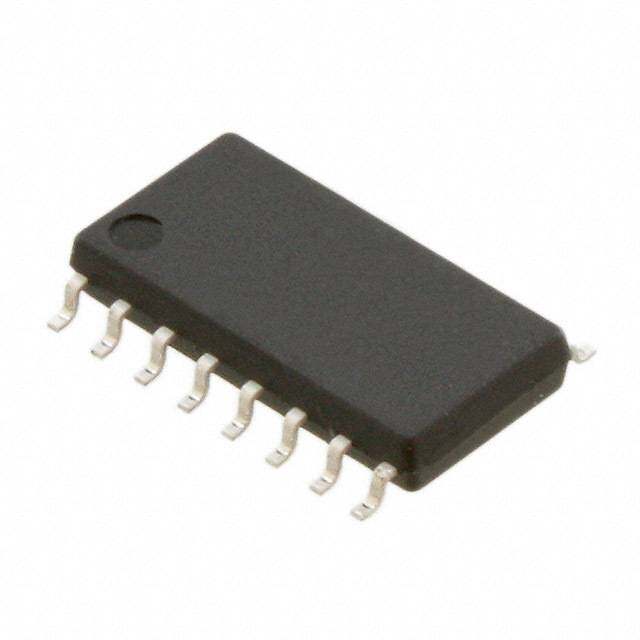
| 描述 | IC FILTER VIDEO 6CH HD/SD 16QSOP视频 IC 6-CH HD/SD Video Filter |
| 产品分类 | |
| 品牌 | Analog Devices |
| 产品手册 | |
| 产品图片 |
|
| rohs | 符合RoHS无铅 / 符合限制有害物质指令(RoHS)规范要求 |
| 产品系列 | 多媒体 IC,视频 IC,Analog Devices ADA4420-6ARQZ- |
| 数据手册 | |
| 产品型号 | ADA4420-6ARQZ |
| 产品目录页面 | |
| 产品种类 | 视频 IC |
| 供应商器件封装 | 16-QSOP |
| 包装 | 管件 |
| 商标 | Analog Devices |
| 安装类型 | 表面贴装 |
| 安装风格 | SMD/SMT |
| 封装 | Tube |
| 封装/外壳 | 16-SSOP(0.154",3.90mm 宽) |
| 封装/箱体 | QSOP-16 |
| 工作电源电压 | 4.75 V to 5.25 V |
| 工厂包装数量 | 98 |
| 带宽 | 10 MHz |
| 应用 | DVD,HD,机顶盒,录音机 |
| 最大工作温度 | + 85 C |
| 最小工作温度 | - 40 C |
| 标准包装 | 98 |
| 电源电流 | 31 mA |
| 类型 | Video Filters |
| 系列 | ADA4420-6 |


PDF Datasheet 数据手册内容提取
Low Cost 6-Channel HD/SD Video Filter ADA4420-6 FEATURES FUNCTIONAL BLOCK DIAGRAM Sixth-order filters INSD1 OUTSD1 Transparent input sync tip clamp ×1 SD ×2 −1 dB bandwidth of 26 MHz typical for HD CLAMP HD rejection @ 75 MHz: 48 dB typical INSD2 OUTSD2 NTSC differential gain: 0.19% ×1 SD ×2 NTSC differential phase: 0.76° CLAMP Rail-to-rail outputs INSD3 OUTSD3 Low quiescent current: 32 mA typical ×1 SD ×2 Disable feature CLAMP DIS Output dc offset INHD1 OUTHD1 APPLICATIONS ×1 HD ×2 CLAMP Set-top boxes DVD players and recorders INHD2 OUTHD2 ×1 HD ×2 HDTVs CLAMP Projectors Personal video recorders INHD3 OUTHD3 ×1 HD ×2 CLAMP ADA4420-6 07532-001 Figure 1. GENERAL DESCRIPTION The ADA4420-6 is a low cost video reconstruction filter specifically Each channel features a transparent sync tip clamp, allowing ac designed for consumer applications. It consists of six independent coupling of the inputs without requiring dc restoration. sixth-order Butterworth filters/buffers, three for standard The output drivers on the ADA4420-6 have rail-to-rail output definition (Y/C or CVBS) and three for high definition capabilities with 6 dB gain. A built-in offset of 250 mV allows component signals (YPrPb or RGB). the outputs to be dc-coupled, eliminating the need for large The ADA4420-6 operates from a single 5 V supply and has a coupling capacitors. Each output is capable of driving two 75 Ω low quiescent current of 32 mA, making it ideal for applications doubly terminated cables. where power consumption is critical. A disable feature allows The ADA4420-6 is available in either a 16-lead QSOP or a 20-lead for further power conservation by reducing the supply current TSSOP, and operates in the extended industrial temperature to less than 8 μA typical when the device is not in use. range of −40°C to +85°C. Rev. A Information furnished by Analog Devices is believed to be accurate and reliable. However, no responsibility is assumed by Analog Devices for its use, nor for any infringements of patents or other One Technology Way, P.O. Box 9106, Norwood, MA 02062-9106, U.S.A. rights of third parties that may result from its use. Specifications subject to change without notice. No license is granted by implication or otherwise under any patent or patent rights of Analog Devices. Tel: 781.329.4700 www.analog.com Trademarks and registered trademarks are the property of their respective owners. Fax: 781.461.3113 ©2008–2011 Analog Devices, Inc. All rights reserved.
ADA4420-6 TABLE OF CONTENTS Features..............................................................................................1 Typical Performance Characteristics..............................................7 Applications.......................................................................................1 Test Circuits.....................................................................................10 General Description.........................................................................1 Applications Information..............................................................11 Functional Block Diagram..............................................................1 Overview.....................................................................................11 Revision History...............................................................................2 Disable.........................................................................................11 Specifications.....................................................................................3 Input and Output Coupling......................................................11 Absolute Maximum Ratings............................................................4 Printed Circuit Board (PCB) Layout.......................................11 Thermal Resistance......................................................................4 Video Encoder Reconstruction Filter......................................11 Maximum Power Dissipation.....................................................4 Outline Dimensions.......................................................................13 ESD Caution..................................................................................4 Ordering Guide..........................................................................14 Pin Configuration and Function Descriptions.............................5 REVISION HISTORY 5/11—Rev. 0 to Rev. A Added 20-Lead TSSOP Package.......................................Universal Changes to General Description Section......................................1 Changes to Disable Assert Voltage, Disable Assert Time, Disable De-Assert Time Parameters............................................................3 Changes to Table 3, Maximum Power Dissipation Section, and Figure 2.......................................................................................4 Added Figure 4 and Table 5.............................................................6 Changes to Figure 18, Figure 19, and Figure 20.........................10 Updated Outline Dimensions.......................................................13 Changes to Ordering Guide..........................................................14 8/08—Revision 0: Initial Version Rev. A | Page 2 of 16
ADA4420-6 SPECIFICATIONS V = 5 V, T = 25°C, V = 2.0 V p-p, R = 150 Ω, dc-coupled inputs, ac-coupled outputs, unless otherwise noted. See Figure 18, Figure 19, S A O L and Figure 20 for the test circuits. Table 1. Parameter Test Conditions/Comments Min Typ Max Unit OVERALL PERFORMANCE DC Voltage Gain All channels 5.8 6.0 6.2 dB Input Voltage Range, All Inputs 0 to 2.1 V Output Voltage Range, All Outputs 0.25 to 4.6 V Linear Output Current per Channel 30 mA Filter Input Bias Current 1 μA SD CHANNEL DYNAMIC PERFORMANCE −1 dB Bandwidth 8.6 MHz −3 dB Bandwidth 8.5 10 MHz Out-of-Band Rejection f = 27 MHz 42 45 dB Crosstalk f = 1 MHz −68 dB Total Harmonic Distortion f = 1 MHz, V = 1.4 V p-p, dc-coupled outputs 0.02 % O Signal-to-Noise Ratio f = 100 kHz to 6 MHz, unweighted 70 dB Propagation Delay 57 ns Group Delay Variation f = 100 kHz to 5 MHz 16 ns Differential Gain NTSC; ac-coupled inputs, dc-coupled outputs; 0.19 % see Figure 19 Differential Phase NTSC; ac-coupled inputs, dc-coupled outputs; 0.76 Degrees see Figure 19 HD CHANNEL DYNAMIC PERFORMANCE −1 dB Bandwidth 26 MHz −3 dB Bandwidth 27 31 MHz Out-of-Band Rejection f = 75 MHz 43 48 dB Crosstalk f = 1 MHz −68 dB Total Harmonic Distortion f = 10 MHz, V = 1.4 V p-p, dc-coupled outputs 0.57 % O Signal-to-Noise Ratio f = 100 kHz to 30 MHz, unweighted 66 dB Propagation Delay 15 ns Group Delay Variation f = 100 kHz to 30 MHz 11 ns DC CHARACTERISTICS Operating Voltage 4.75 to 5.25 V Quiescent Supply Current Active, DIS = 1 32 36 mA Disabled, DIS = 0 7 13 μA PSRR HD channel, referred to output 35 41 dB SD channel, referred to output 40 45 dB Output DC Offset All channels 135 250 375 mV Disable Assert Voltage DIS = 0 to 1 1.9 V Disable Assert Time DIS = 0 to 1 20 ns Disable De-Assert Time DIS = 1 to 0 450 ns Disable Input Bias Current Disabled, DIS = 0 −6.8 μA Input-to-Output Isolation Disabled, DIS = 0, f = 5 MHz −96 dB Rev. A | Page 3 of 16
ADA4420-6 ABSOLUTE MAXIMUM RATINGS The power dissipated in the package (P ) is the sum of the D Table 2. quiescent power dissipation and the power dissipated in the Parameter Rating package due to the load drive for all outputs. The quiescent Supply Voltage 5.5 V power is the voltage between the supply pins (VS) times the Power Dissipation See Figure 2 quiescent current (IS). The power dissipated due to load drive Storage Temperature Range −65°C to +125°C depends on the particular application. For each output, the Operating Temperature Range −40°C to +85°C power due to load drive is calculated by multiplying the load Lead Temperature (Soldering, 10 sec) 300°C current by the associated voltage drop across the device. The power dissipated due to the loads is equal to the sum of the Junction Temperature 150°C power dissipations due to each individual load. RMS voltages Stresses above those listed under Absolute Maximum Ratings and currents must be used in these calculations. may cause permanent damage to the device. This is a stress Airflow increases heat dissipation, effectively reducing θ . rating only; functional operation of the device at these or any JA Figure 2 shows the maximum power dissipation in the package other conditions above those indicated in the operational vs. the ambient temperature for the 16-lead QSOP (105°C/W) section of this specification is not implied. Exposure to absolute and the 20-lead TSSOP (143°C/W) on a JEDEC standard 4-layer maximum rating conditions for extended periods may affect board. θ values are approximate. device reliability. JA 2.0 THERMAL RESISTANCE 1.8 θJA is specified for the device soldered to a high thermal W) conductivity 4-layer (2s2p) circuit board, as described in N ( 1.6 O EIA/JESD 51-7. PATI 1.4 16-LEAD QSOP SI 1.2 S Table 3. DI R 1.0 Package Type θJA θ JC Unit WE O 0.8 16-Lead QSOP 105 23 °C/W P 20-LEAD TSSOP 20-Lead TSSOP 143 45 °C/W UM 0.6 M AXI 0.4 M MAXIMUM POWER DISSIPATION 0.2 The maximum safe power dissipation in the ADA4420-6 0 package is limited by the associated rise in junction temperature 0 10 20 A3M0BIEN4T0 TEM5P0ERAT60URE (7°0C) 80 90 100 07532-016 (TJ) on the die. At approximately 150°C, which is the glass Figure 2. Maximum Power Dissipation vs. transition temperature, the plastic changes its properties. Even Ambient Temperature for a 4-Layer Board temporarily exceeding this temperature limit can change the stresses that the package exerts on the die, permanently shifting ESD CAUTION the parametric performance of the ADA4420-6. Exceeding a junction temperature of 150°C for an extended time can result in changes in the silicon devices, potentially causing failure. Rev. A | Page 4 of 16
ADA4420-6 PIN CONFIGURATION AND FUNCTION DESCRIPTIONS INSD1 1 16 OUTSD1 INSD2 2 15 OUTSD2 INSD3 3 14 OUTSD3 VCC 4 ADA4420-6 13 GND TOP VIEW DIS 5 12 GND (Not to Scale) INHD1 6 11 OUTHD1 INHD2 7 10 OUTHD2 INHD3 8 9 OUTHD3 07532-002 Figure 3. 16-Lead QSOP Pin Configuration Table 4. 16-Pin QSOP Pin Function Descriptions Pin No. Mnemonic Description 1 INSD1 Standard Definition Input 1 2 INSD2 Standard Definition Input 2 3 INSD3 Standard Definition Input 3 4 VCC Power Supply 5 DIS Disable/Power-Down Input 6 INHD1 High Definition Input 1 7 INHD2 High Definition Input 2 8 INHD3 High Definition Input 3 9 OUTHD3 High Definition Output 3 10 OUTHD2 High Definition Output 2 11 OUTHD1 High Definition Output 1 12 GND Ground 13 GND Ground 14 OUTSD3 Standard Definition Output 3 15 OUTSD2 Standard Definition Output 2 16 OUTSD1 Standard Definition Output 1 Rev. A | Page 5 of 16
ADA4420-6 INSD1 1 20 OUTSD1 INSD2 2 19 OUTSD2 INSD3 3 18 OUTSD3 NC 4 17 GND VCC 5 ADA4420-6 16 GND TOP VIEW DIS 6 (Not to Scale) 15 NC INHD1 7 14 OUTHD1 INHD2 8 13 OUTHD2 INHD3 9 12 OUTHD3 NC 10 11 NC NDCO =N ONTO CCOONNNNEECCTT.TO THIS PIN. 07532-003 Figure 4. 20-Lead TSSOP Pin Configuration Table 5. 20-lead TSSOP Pin Function Descriptions Pin No. Mnemonic Description 1 INSD1 Standard Definition Input 1. 2 INSD2 Standard Definition Input 2. 3 INSD3 Standard Definition Input 3. 4 NC Do not connect to this pin. 5 VCC Power Supply. 6 DIS Disable/Power Down Input. 7 INHD1 High Definition Input 1. 8 INHD2 High Definition Input 2. 9 INHD3 High Definition Input 3. 10 NC Do not connect to this pin. 11 NC Do not connect to this pin. 12 OUTHD3 High Definition Output 3. 13 OUTHD2 High Definition Output 2. 14 OUTHD1 High Definition Output 1. 15 NC No Connection. 16 GND Ground. 17 GND Ground. 18 OUTSD3 Standard Definition Output 3. 19 OUTSD2 Standard Definition Output 2. 20 OUTSD1 Standard Definition Output 1. Rev. A | Page 6 of 16
ADA4420-6 TYPICAL PERFORMANCE CHARACTERISTICS V = 5 V, T = 25°C, V = 2.0 V p-p, R = 150 Ω, dc-coupled inputs, ac-coupled outputs, unless otherwise noted. See Figure 18, Figure 19, S A O L and Figure 20 for the test circuits. 10 1.0 HD CHANNELS, SD CHANNELS, 0 RL = 75Ω 0.5 RL = 75Ω HD CHANNELS, HD CHANNELS, RL = 75Ω –10 RL = 150Ω 0 B) N (dB) ––3200 SD CHANNELS, SRDL =C H75AΩNNELS, ED GAIN (d––10..05 SRDL =C H15A0NΩNELS, HRDL =C 1H5A0NΩNELS, GAI –40 RL = 150Ω LIZ MA–1.5 –50 R O N–2.0 –60 –70 –2.5 –80 –3.0 1 FR1E0QUENCY (MHz) 100 07532-004 1 FREQUE1N0CY (MHz) 100 07532-007 Figure 5. Frequency Response vs. Load (RL) Figure 8. Flatness vs. Load (RL) 10 1.0 0 0.5 –10 0 B) –20 N (d–0.5 N (dB) –30 ED GAI–1.0 GAI –40 LIZ MA–1.5 –50 R O HD –40°C N–2.0 HD –40°C –60 HD +25°C HD +25°C HD +85°C HD +85°C –70 SSDD –+4205°°CC –2.5 SSDD –+4205°°CC SD +85°C SD +85°C –80 –3.0 1 FREQ10UENCY (MHz) 100 07532-005 1 FREQUE1N0CY (MHz) 100 07532-008 Figure 6. Frequency Response vs. Temperature Figure 9. Flatness vs. Temperature 10 10 HD DC-COUPLED 0 0 –10 –10 HD AC-COUPLED –20 –20 dB) –30 dB) –30 N ( N ( AI –40 AI –40 G G –50 –50 –60 –60 –70 SSHHDDDD VVVVOOOO ==== 21120.0.0000VVmm ppVV-- pppp--pp –70 SDSD D ACC-C-COOUUPLPELDED –80 –80 1 FREQ10UENCY (MHz) 100 07532-006 1 FREQ10UENCY (MHz) 100 07532-017 Figure 7. Frequency Response vs. Amplitude Figure 10. Frequency Response vs. Output Coupling Rev. A | Page 7 of 16
ADA4420-6 100 6 90 5 80 SD CHANNELS 70 4 ns) V) AY ( 60 GE ( 3 L A DE 50 SD CHANNELS LT OUP 40 S VO 2 HD CHANNELS R DI G 30 1 HD CHANNELS 20 0 10 0 –1 0.1 1FREQUENCY (MHz)10 100 07532-009 –600 –400 –200 0 2T0I0ME (n40s0) 600 800 1000 120007532-012 Figure 11. Group Delay vs. Frequency Figure 13. Enable Time 10k 36 DIS = 0 35 34 Ω) A) DANCE ( 1k RENT (m 33 MPE CUR 32 UT I LY 31 UTP 100 UPP O S 30 29 10 28 0.1 1 FREQUENCY (M1H0z) 100 07532-011 –60 –40 –20 TE0MPERA20TURE (4°0C) 60 80 100 07532-013 Figure 12. Output Impedance vs. Frequency Figure 14. Supply Current vs. Temperature Rev. A | Page 8 of 16
ADA4420-6 0 4.70 –10 4.68 V) –20 E (4.66 G A T4.64 B) –30 OL LK (d –40 ON V4.62 A TI4.60 T A ROSS –50 ATUR4.58 C –60 SD CHANNELS T S4.56 U –70 TP4.54 U O –80 HD CHANNELS 4.52 –90 4.50 0.1 1 FREQUE1N0CY (MHz) 100 100007532-014 –60 –40 –20 TE0MPERA2T0URE (°4C0) 60 80 100 07532-010 Figure 15. Crosstalk vs. Frequency Figure 17. Output Saturation Voltage vs. Temperature 6 5 SD CHANNELS 4 V) E ( G 3 A T L O S V 2 HD CHANNELS DI 1 0 –1 –200 –160 –120 –80 –40TIME0 (ns)40 80 120 160 200 07532-015 Figure 16. Disable Time Rev. A | Page 9 of 16
ADA4420-6 TEST CIRCUITS AGILENT E3631A POWER SUPPLY +6V ±25V + – + COM – ADA4420-6 TEST CIRCUIT VCC (SEE FIGURE 18) VCC GND DIS INxDx OUTxDx 0.1µF 10µF 50Ω VIN 220µF PORT 1 PORT 2 49.9Ω ADA4420-6 VOUT BIAS 118Ω CONNECT 86.6Ω PORT 1 DIS GND 07532-018 AGILENT 8753D VECTOR NETWORK ANALYZER 07532-020 Figure 18. DC-Coupled Input, AC-Coupled Output Figure 20. Test Circuit for Frequency Response and Group Delay VCC 0.1µF 10µF VIN 0.1µF 49.9Ω ADA4420-6 VOUT 118Ω 86.6Ω DIS GND 07532-019 Figure 19. AC-Coupled Input, DC-Coupled Output Rev. A | Page 10 of 16
ADA4420-6 APPLICATIONS INFORMATION OVERVIEW 75Ω ADA4420-6 75Ω 220µF CABLE With its high impedance inputs and high output drive, the ADA4420-6 is ideally suited to video reconstruction and anti- 75Ω 75Ω alias filtering applications. The high impedance inputs give 75Ω 220µF CABLE designers flexibility with regard to how the input signals are ttehrem AiDnaAte4d4.2 D0-e6v iccaens bwei tlho aDdAedC icnu wrrheantte svoeur rrcees iostuatnpcuet sp trhoavti dfeeesd 75Ω 07532-022 the best performance, and devices with voltage outputs can be Figure 21. Driving Two AC-Coupled Loads with Two Coupling Capacitors optimally terminated as well. The ADA4420-6 outputs can each 75Ω drive up to two source-terminated, 75 Ω loads and; therefore, can ADA4420-6 75Ω CABLE directly drive the outputs from set-top boxes and DVDs without 470µF 75Ω the need for a separate output buffer. 75Ω CABLE 75Ω DISABLE Tsahvee pAoDwAer4 4w2h0e-n6 ain pcalrutdiceusl aar d diesvaibclee ifse natout rien tuhsaet. cWanh ebne duisseabdl etod , 75Ω 07532-023 Figure 22. Driving Two AC-Coupled Loads with One Common Coupling Capacitor the ADA4420-6 typically draws only 7 μA from the supply. The disable feature is asserted by pulling the DIS pin low. PRINTED CIRCUIT BOARD (PCB) LAYOUT Table 6 summarizes the operation of the disable feature. As with all high speed applications, attention to the PCB layout is of paramount importance. When designing with the ADA4420-6, Table 6. Disable Function adhere to standard high speed layout practices. A solid ground DIS Pin Connection Status plane is recommended, and surface-mount, ceramic power supply V or Floating Enabled decoupling capacitors should be placed as close as possible to the CC GND Disabled supply pins. Connect all of the ADA4420-6 GND pins to the ground plane with traces that are as short as possible. Controlled INPUT AND OUTPUT COUPLING impedance traces of the shortest length possible should be used to connect to the signal I/O pins and should not pass over any Inputs to the ADA4420-6 can be ac- or dc-coupled. For dc-coupled voids in the ground plane. A 75 Ω impedance level is typically inputs, the signal must be completely contained within the input used in video applications. When driving transmission lines, range of 0 V to 2.1 V. When using ac-coupled inputs, the lowest include series termination resistors on the signal outputs of the point of the signal is clamped to approximately 0 V. The ADA4420-6 ADA4420-6. outputs can be either ac- or dc-coupled. When the ADA4420-6 receives its inputs from a device with When driving single ac-coupled loads in standard 75 Ω video current outputs, the required load resistor value for the output distribution systems, a minimum capacitance of 220 μF is current is often different from the characteristic impedance of recommended to avoid line and field droop. There are two ac the signal traces. In this case, if the interconnections are short coupling options when driving two loads from one output. One (<< 0.1 wavelength), the trace does not have to be terminated in option simply uses the same value capacitor on the second load, its characteristic impedance. Traces of 75 Ω can be used in this while the other option uses a common coupling capacitor that instance, provided their lengths are an inch or two at most. This is at least twice the value used for the single load (see Figure 21 is easily achieved because the ADA4420-6 and the device feeding it and Figure 22). are usually adjacent to each other, and connections can be made When driving two parallel 150 Ω loads (75 Ω effective load), the that are less than one inch in length. 3 dB bandwidth of the filters typically varies from that of the filters VIDEO ENCODER RECONSTRUCTION FILTER with a single 150 Ω load (see Figure 5). The ADA4420-6 is easily applied as a reconstruction filter at the DAC outputs of a video encoder. Figure 23 illustrates how to use the ADA4420-6 in this type of application following an ADV734x series video encoder, with a single-supply and ac-coupled outputs. Rev. A | Page 11 of 16
ADA4420-6 AMDULVT7IF3O4xRMAT DAC 1 INHD1 ×1 HD ×2 OUTHD1 2+20μF 75Ω Y VIDEO ENCODER 300Ω DAC 2 INHD2 ×1 HD ×2 OUTHD2 2+20μF 75Ω Pb 300Ω DAC 3 INHD3 ×1 HD ×2 OUTHD3 2+20μF 75Ω Pr 300Ω DIS ADA4420-6 INSD1 OUTSD1 220μF 75Ω DAC 4 ×1 SD ×2 + CVBS 300Ω INSD2 OUTSD2 220μF 75Ω DAC 5 ×1 SD ×2 + 300Ω S-VIDEO INSD3 OUTSD3 220μF 75Ω DAC 6 ×1 SD ×2 + RSET1 RSET2 300Ω 4.12kΩ 4.12kΩ 07532-021 Figure 23. The ADA4420-6 Applied as a Reconstruction Filter Following an ADV734x Series Video Encoder Rev. A | Page 12 of 16
ADA4420-6 OUTLINE DIMENSIONS 0.197(5.00) 0.193(4.90) 0.189(4.80) 16 9 0.158(4.01) 0.154(3.91) 0.150(3.81) 0.244(6.20) 1 0.236(5.99) 8 0.228(5.79) 0.010(0.25) 0.020(0.51) 0.065(1.65) 0.069(1.75) 0.006(0.15) 0.010(0.25) 0.049(1.25) 0.053(1.35) 0.010(0.25) CO0P.00L.00A40N(40A.(10R0.I1)T0Y) 0.02B5S(C0.64) 0.012(0.30) SPELAATNIENG 80°° 00..005106((10..2471)) 0R.E04F1(1.04) 0.008(0.20) COMPLIANTTOJEDECSTANDARDSMO-137-AB C(RINOEFNPEATRRREOENNLCLTEIHNEOGSNDELISYM)AEANNRDSEIAORRNOESUNANORDETEDAIN-POIPNFRFCOHINPECRSHI;AMTEEQILUFLOIIVMRAELUTEESNRETDISNIMFDOEERNSSIGIONN.S 01-28-2008-A Figure 24. 16-Lead Shrink Small Outline Package [QSOP] (RQ-16) Dimensions shown in inches and (millimeters) 6.60 6.50 6.40 20 11 4.50 4.40 4.30 6.40 BSC 1 10 PIN 1 0.65 BSC 0.15 1.20 MAX 0.20 0.05 0.09 0.75 0.30 8° 0.60 COPLANARITY 0.19 SEATING 0° 0.45 0.10 PLANE COMPLIANT TO JEDEC STANDARDS MO-153-AC Figure 25. 20-Lead Thin Shrink Small Outline Package [TSSOP] (RU-20) Dimensions shown in millimeters Rev. A | Page 13 of 16
ADA4420-6 ORDERING GUIDE Temperature Model1 Range Package Description Package Option Ordering Quantity ADA4420-6ARQZ −40°C to +85°C 16-Lead Shrink Small Outline Package (QSOP) RQ-16 Tube (98) ADA4420-6ARQZ-R7 −40°C to +85°C 16-Lead Shrink Small Outline Package (QSOP) RQ-16 1,000 ADA4420-6ARQZ-RL −40°C to +85°C 16-Lead Shrink Small Outline Package (QSOP) RQ-16 2,500 ADA4420-6ARUZ −40°C to +85°C 20-Lead Thin Shrink Small Outline Package (TSSOP) RU-20 Tube (75) ADA4420-6ARUZ-R7 −40°C to +85°C 20-Lead Thin Shrink Small Outline Package (TSSOP) RU-20 1,000 ADA4420-6ARUZ-RL −40°C to +85°C 20-Lead Thin Shrink Small Outline Package (TSSOP) RU-20 2,500 1 Z = RoHS Compliant Part. Rev. A | Page 14 of 16
ADA4420-6 NOTES Rev. A | Page 15 of 16
ADA4420-6 NOTES ©2008–2011 Analog Devices, Inc. All rights reserved. Trademarks and registered trademarks are the property of their respective owners. D07532-0-5/11(A) Rev. A | Page 16 of 16