ICGOO在线商城 > 集成电路(IC) > 线性 - 放大器 - 仪表,运算放大器,缓冲器放大器 > ADA4062-2ACPZ-R7
 Datasheet下载
- 型号: ADA4062-2ACPZ-R7
- 制造商: Analog
- 库位|库存: xxxx|xxxx
- 要求:
| 数量阶梯 | 香港交货 | 国内含税 |
| +xxxx | $xxxx | ¥xxxx |
查看当月历史价格
查看今年历史价格
ADA4062-2ACPZ-R7产品简介:
ICGOO电子元器件商城为您提供ADA4062-2ACPZ-R7由Analog设计生产,在icgoo商城现货销售,并且可以通过原厂、代理商等渠道进行代购。 ADA4062-2ACPZ-R7价格参考¥8.24-¥17.66。AnalogADA4062-2ACPZ-R7封装/规格:线性 - 放大器 - 仪表,运算放大器,缓冲器放大器, J-FET 放大器 2 电路 10-LFCSP-UQ(1.6x1.3)。您可以下载ADA4062-2ACPZ-R7参考资料、Datasheet数据手册功能说明书,资料中有ADA4062-2ACPZ-R7 详细功能的应用电路图电压和使用方法及教程。
ADA4062-2ACPZ-R7 是由 Analog Devices Inc. 生产的一款双通道低噪声、低功耗运算放大器,属于线性 - 放大器 - 仪表、运算放大器、缓冲器放大器类别。其主要应用场景包括:

1. 医疗设备:
   ADA4062-2ACPZ-R7 的低噪声特性和高精度使其非常适合用于医疗电子设备,例如心电图(ECG)、脑电图(EEG)和超声波设备中的信号调理电路。这些应用需要对微弱的生物电信号进行精确放大,同时避免引入噪声。

2. 工业自动化与控制:
   在工业领域中,该器件可用于传感器信号放大,例如温度传感器、压力传感器和加速度传感器等。其低偏移电压和漂移特性确保了在复杂工业环境下的高精度测量。

3. 数据采集系统 (DAQ):
   这款放大器适用于多通道数据采集系统,能够对来自不同传感器的输入信号进行缓冲和放大,同时保持低噪声和高稳定性,从而提高系统的整体性能。

4. 音频处理:
   虽然 ADA4062-2ACPZ-R7 并非专门设计为音频放大器,但其低失真和低噪声特性使其可以用于高品质音频前置放大器或麦克风信号放大器中。

5. 便携式设备:
   由于其低功耗特性,这款放大器非常适合电池供电的便携式设备,如手持测试仪器、可穿戴健康监测设备等。它能够在保证性能的同时延长设备的续航时间。

6. 汽车电子:
   在汽车行业中,ADA4062-2ACPZ-R7 可用于车载传感器信号处理,例如胎压监测系统(TPMS)、发动机控制单元(ECU)和其他需要高精度信号放大的场景。

综上所述,ADA4062-2ACPZ-R7 凭借其低噪声、低功耗和高精度的特点,广泛应用于需要高性能信号处理的各种领域,特别是在对噪声敏感或需要长时间稳定工作的环境中表现优异。
| 参数 | 数值 |
| -3db带宽 | - |
| 产品目录 | 集成电路 (IC) |
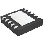
| 描述 | IC OPAMP JFET 1.4MHZ 10-LFCSP |
| 产品分类 | Linear - Amplifiers - Instrumentation, OP Amps, Buffer Amps |
| 品牌 | Analog Devices Inc |
| 数据手册 | |
| 产品图片 |
|
| 产品型号 | ADA4062-2ACPZ-R7 |
| rohs | 无铅 / 符合限制有害物质指令(RoHS)规范要求 |
| 产品系列 | - |
| 产品培训模块 | http://www.digikey.cn/PTM/IndividualPTM.page?site=cn&lang=zhs&ptm=30008http://www.digikey.cn/PTM/IndividualPTM.page?site=cn&lang=zhs&ptm=26202 |
| 供应商器件封装 | 10-LFCSP-UQ(1.6x1.3) |
| 其它名称 | ADA4062-2ACPZ-R7DKR |
| 包装 | Digi-Reel® |
| 压摆率 | 3.3 V/µs |
| 增益带宽积 | 1.4MHz |
| 安装类型 | 表面贴装 |
| 封装/外壳 | 10-UFQFN,CSP |
| 工作温度 | -40°C ~ 125°C |
| 放大器类型 | J-FET |
| 标准包装 | 1 |
| 电压-电源,单/双 (±) | 8 V ~ 36 V, ±4 V ~ 18 V |
| 电压-输入失调 | 750µV |
| 电流-电源 | 165µA |
| 电流-输入偏置 | 2pA |
| 电流-输出/通道 | 20mA |
| 电路数 | 2 |
| 视频文件 | http://www.digikey.cn/classic/video.aspx?PlayerID=1364138032001&width=640&height=505&videoID=2245193153001http://www.digikey.cn/classic/video.aspx?PlayerID=1364138032001&width=640&height=505&videoID=2245193159001 |
| 设计资源 | |
| 输出类型 | - |


- 商务部:美国ITC正式对集成电路等产品启动337调查
- 曝三星4nm工艺存在良率问题 高通将骁龙8 Gen1或转产台积电
- 太阳诱电将投资9.5亿元在常州建新厂生产MLCC 预计2023年完工
- 英特尔发布欧洲新工厂建设计划 深化IDM 2.0 战略
- 台积电先进制程称霸业界 有大客户加持明年业绩稳了
- 达到5530亿美元!SIA预计今年全球半导体销售额将创下新高
- 英特尔拟将自动驾驶子公司Mobileye上市 估值或超500亿美元
- 三星加码芯片和SET,合并消费电子和移动部门,撤换高东真等 CEO
- 三星电子宣布重大人事变动 还合并消费电子和移动部门
- 海关总署:前11个月进口集成电路产品价值2.52万亿元 增长14.8%


PDF Datasheet 数据手册内容提取
Low Power JFET-Input Op Amps ADA4062-2/ADA4062-4 FEATURES PIN CONFIGURATIONS Low input bias current: 50 pA maximum OUT A 1 8 V+ Offset voltage ADA4062-2 –IN A 2 7 OUT B Of12fs..e55t mm voVVl tmmaaagxxeii mmdruuifmmt: 5ffoo μrr VBA/ °ggCrr aatdydpee i (cAaDl A4062-2 SOIC package) +INV A– 34 (NToOt Pto V SIEcaWle) 65 –+IINN BB 07670-001 Figure 1. 8-Lead Narrow-Body SOIC and 8-Lead MSOP Slew rate: 3.3 V/μs typical A CMRR: 90 dB typical T U C + Low supply current: 165 μA typical O N V 0 1 1 9 High input impedance Unity-gain stable –IN A2 8OUT B ±5 V to ±15 V dual-supply operation ADA4062-2 Packaging +IN A3 TOP VIEW 7–IN B (Not to Scale) 8-lead SOIC, 8-lead MSOP, 10-lead LFCSP, 14-lead TSSOP, and APP1L6I-CleAaTd ILOFCNSSP packages NC = NO CONNECT –V4 5CN B N6I+ 07670-065 Figure 2. 10-Lead LFCSP Power controls and monitoring Active filters OUT A 1 14 OUT D Industrial/process controls –IN A 2 13 –IN D Body probe electronics +IN A 3 ADA4062-4 12 +IN D Data acquisition V+ 4 (NToOt Pto V SIEcaWle) 11 V– Integrators +IN B 5 10 +IN C Input buffering –IN B 6 9 –IN C GENERAL DESCRIPTION OUT B 7 8 OUT C 07670-064 The ADA4062-2 and ADA4062-4 are dual and quad JFET-input Figure 3. 14-Lead TSSOP amplifiers with industry-leading performance. They offer lower A D T T power, offset voltage, drift, and ultralow bias current. The NC OU OU NC ADA4062-2 B grade (SOIC package) features a typical low offset 61 51 41 31 voltage of 0.5 mV, an offset drift of 5 μV/°C, and a bias current –INA 1 12 –IND of 2 pA. +INA 2 ADA4062-4 11 +IND The ADA4062 family is ideal for various applications, including V+ 3 (NToOt Pto V SIEcaWle) 10 V– process controls, industrial and instrumentation equipment, +INB 4 9 +INC active filtering, data conversion, buffering, and power control 5 6 7 8 and monitoring. With a low supply current of 165 μA per B B C C N T T N amplifier, they are well suited for lower power applications. –I OU OU –I Ttehme pAeDraAtu4r0e6 r2a fnagmei loyf i−s 4al0s°oC s ptoec +if1ie2d5 °foCr. tThhe ee xAteDnAde4d0 6in2d-2u sitsr ial N12..O NITTC EISS= RNEOCOCOMNMNEENCDTE.D TO CONNECT THE EXPOSED PAD TO V–. 07670-068 Figure 4. 16-Lead LFCSP available in lead-free, 8-lead SOIC, 8-lead MSOP, and 10-lead LFCSP (1.6 mm × 1.3 mm × 0.55 mm) packages, while the Table 1. Low Power Op Amps ADA4062-4 is available in lead-free, 14-lead TSSOP and Precision Precision High 16-lead LFCSP packages. CMOS High Bandwidth Bandwidth Single AD8663 AD8641 Dual AD8667 AD8642 AD8682 Quad AD8669 AD8643 AD8684 Rev. B Information furnished by Analog Devices is believed to be accurate and reliable. However, no responsibility is assumed by Analog Devices for its use, nor for any infringements of patents or other One Technology Way, P.O. Box 9106, Norwood, MA 02062-9106, U.S.A. rights of third parties that may result from its use. Specifications subject to change without notice. No license is granted by implication or otherwise under any patent or patent rights of Analog Devices. Tel: 781.329.4700 www.analog.com Trademarks and registered trademarks are the property of their respective owners. Fax: 781.461.3113 ©2008–2010 Analog Devices, Inc. All rights reserved.
ADA4062-2/ADA4062-4 TABLE OF CONTENTS Features .............................................................................................. 1 ESD Caution...................................................................................5 Applications ....................................................................................... 1 Typical Performance Characteristics ..............................................6 General Description ......................................................................... 1 Applications Information .............................................................. 15 Pin Configurations ........................................................................... 1 Notch Filter ................................................................................. 15 Revision History ............................................................................... 2 High-Side Signal Conditioning ................................................ 15 Specifications ..................................................................................... 3 Micropower Instrumentation Amplifier ................................. 15 Electrical Characteristics ............................................................. 3 Phase Reversal ............................................................................ 16 Absolute Maximum Ratings ............................................................ 5 Schematic ......................................................................................... 17 Thermal Resistance ...................................................................... 5 Outline Dimensions ....................................................................... 18 Power Sequencing ........................................................................ 5 Ordering Guide .......................................................................... 20 REVISION HISTORY 2/10—Rev. A to Rev. B 7/09—Rev. 0 to Rev. A Added 16-Lead LFCSP Package........................................ Universal Added ADA4062-4 ............................................................. Universal Changes to Features Section, General Description Section, and Added 14-Lead TSSOP Package ....................................... Universal Table 1 ................................................................................................ 1 Added 10-Lead LFCSP Package ....................................... Universal Changes to Offset Voltage Drift Parameter, Table 2 .................... 3 Changes to Features Section and Table 1 ....................................... 1 Changes to Table 4 ............................................................................ 5 Changes to Table 2 ............................................................................. 3 Changes to Typical Performance Characteristics Layout ............ 6 Changes to Thermal Resistance Section ........................................ 5 Added Figure 6 and Figure 9; Renumbered Sequentially ........... 6 Changes to Figure 5, Figure 6, Figure 8, and Figure 9 .................. 6 Changes to Figure 7, Figure 8, and Figure 10 ............................... 6 Changes to Figure 37 and Figure 40............................................. 11 Changes to Figure 25 and Figure 28 ............................................... 9 Changes to Figure 41 and Figure 44............................................. 12 Changes to Figure 37 and Figure 40 ............................................. 11 Changes to Figure 47, Figure 48, Figure 50, and Figure 51....... 13 Changes to Figure 41 to Figure 46 ................................................ 12 Added Figure 49 and Figure 52; Renumbered Sequentially ..... 13 Changes to Figure 47 and Figure 50 ............................................. 13 Changes to Figure 57 and Figure 59............................................. 15 Changes to Figure 53 to Figure 58 ................................................ 14 Changes to Phase Reversal Section and Figure 61 ..................... 16 Changes to Notch Filter Section and Micropower Instrumentation Changes to Figure 63 ...................................................................... 17 Amplifier Section ............................................................................ 15 Updated Outline Dimensions ....................................................... 18 Updated Outline Dimensions ....................................................... 18 Changes to Ordering Guide .......................................................... 19 Changes to Ordering Guide .......................................................... 20 10/08—Revision 0: Initial Version Rev. B | Page 2 of 20
ADA4062-2/ADA4062-4 SPECIFICATIONS ELECTRICAL CHARACTERISTICS V = ±15 V, V = 0 V, T = 25°C, unless otherwise noted. SY CM A Table 2. Parameter Symbol Conditions Min Typ Max Unit INPUT CHARACTERISTICS Offset Voltage V OS B Grade (ADA4062-2, 8-Lead SOIC Only) 0.5 1.5 mV −40°C ≤ T ≤ +125°C 3 mV A A Grade 0.75 2.5 mV −40°C ≤ T ≤ +125°C 5 mV A Offset Voltage Drift ∆V /∆T −40°C ≤ T ≤ +125°C 5 μV/°C OS A Input Bias Current I 2 50 pA B −40°C ≤ T ≤ +125°C 5 nA A Input Offset Current I 0.5 25 pA OS −40°C ≤ T ≤ +125°C 2.5 nA A Input Voltage Range −40°C ≤ T ≤ +125°C −11.5 +15 V A Common-Mode Rejection Ratio CMRR B Grade (ADA4062-2, 8-Lead SOIC Only) V = −11.5 V to +11.5 V 80 90 dB CM −40°C ≤ T ≤ +125°C 80 dB A A Grade V = −11.5 V to +11.5 V 73 90 dB CM −40°C ≤ T ≤ +125°C 70 dB A Large-Signal Voltage Gain A R = 10 kΩ, V = −10 V to +10 V 76 83 dB VO L O −40°C ≤ T ≤ +125°C 72 dB A Input Resistance R 10 TΩ IN Input Capacitance, Differential Mode C 1.5 pF INDM Input Capacitance, Common Mode C 4.8 pF INCM OUTPUT CHARACTERISTICS Output Voltage High V R = 10 kΩ to V 13 13.5 V OH L CM −40°C ≤ T ≤ +125°C 12.5 V A Output Voltage Low V R = 10 kΩ to V −13.8 −13 V OL L CM −40°C ≤ T ≤ +125°C −12.5 V A Short-Circuit Current I 20 mA SC Closed-Loop Output Impedance Z f = 1 kHz, A = 1 1 Ω OUT V POWER SUPPLY Power Supply Rejection Ratio PSRR B Grade (ADA4062-2, 8-Lead SOIC Only) V = ±4 V to ±18 V 80 90 dB SY −40°C ≤ T ≤ +125°C 80 dB A A Grade V = ±4 V to ±18 V 74 90 dB SY −40°C ≤ T ≤ +125°C 70 dB A Supply Current per Amplifier I I = 0 mA 165 220 μA SY O −40°C ≤ T ≤ +125°C 260 μA A DYNAMIC PERFORMANCE Slew Rate SR R = 10 kΩ, C = 100 pF, A = 1 3.3 V/μs L L V Settling Time t To 0.1%, V = 10 V step, C = 100 pF, 3.5 μs S IN L R = 10 kΩ, A = 1 L V Gain Bandwidth Product GBP R = 10 kΩ, A = 1 1.4 MHz L V Phase Margin Φ R = 10 kΩ, A = 1 78 Degrees M L V Channel Separation (ADA4062-2 Only) CS f = 1 kHz 135 dB Channel Separation (ADA4062-4 Only) CS f = 1 kHz 130 dB Rev. B | Page 3 of 20
ADA4062-2/ADA4062-4 Parameter Symbol Conditions Min Typ Max Unit NOISE PERFORMANCE Voltage Noise e p-p f = 0.1 Hz to 10 Hz 1.5 μV p-p n Voltage Noise Density e f = 1 kHz 36 nV/√Hz n Current Noise Density i f = 1 kHz 5 fA/√Hz n Rev. B | Page 4 of 20
ADA4062-2/ADA4062-4 ABSOLUTE MAXIMUM RATINGS THERMAL RESISTANCE Table 3. Parameter Rating θ is specified for the worst-case conditions, that is, a device JA Supply Voltage ±18 V soldered in a circuit board for surface-mount packages. It was Input Voltage ±V measured using a standard 4-layer board. SY Differential Input Voltage ±V SY Table 4. Thermal Resistance Input Current ±10 mA Package Type θ θ Unit Output Short-Circuit Duration to GND Indefinite JA JC 8-Lead SOIC 120 45 °C/W Storage Temperature Range −65°C to +150°C 8-Lead MSOP 142 45 °C/W Operating Temperature Range −40°C to +125°C 10-Lead LFCSP 132 46 °C/W Junction Temperature Range −65°C to +150°C 14-Lead TSSOP 112 35 °C/W Lead Temperature (Soldering, 60 sec) 300°C 16-Lead LFCSP 75 12 °C/W Stresses above those listed under Absolute Maximum Ratings POWER SEQUENCING may cause permanent damage to the device. This is a stress rating only; functional operation of the device at these or any The supply voltages of the op amps must be established other conditions above those indicated in the operational simultaneously with, or before, any input signals are applied. If section of this specification is not implied. Exposure to absolute this is not possible, the input current must be limited to 10 mA. maximum rating conditions for extended periods may affect device reliability. ESD CAUTION Rev. B | Page 5 of 20
ADA4062-2/ADA4062-4 TYPICAL PERFORMANCE CHARACTERISTICS T = 25°C, unless otherwise noted. A 70 280 VSY = ±5V VSY = ±15V VCM = 0V VCM = 0V 60 BASED ON 600 OP AMPS 240 BASED ON 600 OP AMPS RS 50 RS 200 E E F F LI LI MP 40 MP 160 A A F F O O R 30 R 120 E E B B M M U 20 U 80 N N 10 40 0–4 –3 –2 –1 VOS 0(mV) 1 2 3 4 07670-054 0–4 –3 –2 –1 VOS 0(mV) 1 2 3 4 07670-003 Figure 5. Input Offset Voltage Distribution Figure 8. Input Offset Voltage Distribution 40 40 ADA4062-2 ONLY ADA4062-2 ONLY VSY = ±5V VSY = ±15V –40°C ≤ TA ≤ +125°C –40°C ≤ TA ≤ +125°C BASED ON 200 OP AMPS BASED ON 200 OP AMPS S 30 S 30 R R E E F F LI LI P P M M F A 20 F A 20 O O R R E E B B M M U U N 10 N 10 0–2 0 2 TCVOS 4(µV/°C) 6 8 10 07670-055 0–2 0 2 TCVOS 4(µV/°C) 6 8 10 07670-005 Figure 6. Input Offset Voltage Drift Distribution Figure 9. Input Offset Voltage Drift Distribution 25 25 ADA4062-4 ONLY ADA4062-4 ONLY VSY = ±5V VSY = ±15V –40°C ≤ T≤ 125°C –40°C ≤ T≤ 125°C 20 BASED ON 200 OPAMPS 20 BASED ON 200 OPAMPS S S R R E E FI FI LI 15 LI 15 P P M M A A F F O O R 10 R 10 E E B B M M U U N N 5 5 0 0 0 2 4 6 TCV8OS (µV1/0°C) 12 14 16 18 07670-070 0 2 4 6 TCV8OS (µV1/0°C) 12 14 16 18 07670-069 Figure 7. Input Offset Voltage Drift Distribution Figure 10. Input Offset Voltage Drift Distribution Rev. B | Page 6 of 20
ADA4062-2/ADA4062-4 5 5 VSY = ±5V VSY = ±15V 4 4 3 3 2 2 1 1 V) V) m m (S 0 (S 0 O O V –1 V –1 –2 –2 –3 –3 –4 –4 –5–4 –3 –2 –1 0VCM (V1) 2 3 4 5 07670-056 –5–15 –12 –9 –6 –3 VCM0 (V) 3 6 9 12 15 07670-006 Figure 11. Input Offset Voltage vs. Common-Mode Voltage Figure 14. Input Offset Voltage vs. Common-Mode Voltage 10000 10000 VSY = ±5V VSY = ±15V 1000 1000 100 100 A) A) p p (B (B I 10 I 10 1 1 0.1–50 –25 0 TEMP25ERATUR5E0(°C) 75 100 125 07670-012 0.1–50 –25 0 TEMP2E5RATUR5E0(°C) 75 100 125 07670-009 Figure 12. Input Bias Current vs. Temperature Figure 15. Input Bias Current vs. Temperature 3 5 VSY = ±5V VSY = ±15V 2 4 1 3 A) A) p p (B (B I 0 I 2 –1 1 –2–3 –2 –1 0 VCM1 (V) 2 3 4 5 07670-013 0–12–10 –8 –6 –4 –2 0VCM 2(V) 4 6 8 10 12 14 16 07670-010 Figure 13. Input Bias Current vs. Common-Mode Voltage Figure 16. Input Bias Current vs. Common-Mode Voltage Rev. B | Page 7 of 20
ADA4062-2/ADA4062-4 10 10 VSY = ±5V VSY = ±15V V) V) L ( L ( AI AI R R Y Y L L P P UP V+ – VOH UP V+ – VOH S S O O T 1 T 1 GE VOL – V– GE VOL – V– A A T T L L O O V V T T U U P P T T U U O O 0.10.01 0.1 LOAD CUR1RENT (mA) 10 100 07670-014 0.10.01 0.1 LOAD CUR1RENT (mA) 10 100 07670-011 Figure 17. Output Voltage to Supply Rail vs. Load Current Figure 20. Output Voltage to Supply Rail vs. Load Current 220 200 +125°C 200 190 +85°C 180 180 A) A) µ 160 µ P ( P ( 170 T/AM 140 +25°C T/AM 160 VSY = ±15V N 120 N RE –40°C RE 150 UR 100 UR VSY = ±5V C C 140 Y 80 Y L L P P 130 P 60 P U U S 40 S 120 20 110 00 2 4 S6UPPLY8 VOLT1A0GE (±1V2) 14 16 18 07670-146 100–50 –25 0 T2E5MPERA50TURE (7°5C) 100 125 150 07670-149 Figure 18. Supply Current/Amp vs. Supply Voltage Figure 21. Supply Current/Amp vs. Temperature 2.0 2.0 L (V) RVSLY = = 1 0±5kΩV L (V) V+ – VOH RVSLY = = 1 0±k15ΩV AI AI R 1.5 R 1.5 PLY V+ – VOH PLY UP UP VOL – V– S S TO 1.0 VOL – V– TO 1.0 E E G G A A L L T T O O V V T 0.5 T 0.5 U U P P T T U U O O 0–50 –25 0 TEMP2E5RATUR5E0(°C) 75 100 125 07670-018 0–50 –25 0 TEMP25ERATUR5E0 (°C) 75 100 125 07670-015 Figure 19. Output Voltage to Supply Rail vs. Temperature Figure 22. Output Voltage to Supply Rail vs. Temperature Rev. B | Page 8 of 20
ADA4062-2/ADA4062-4 120 120 120 120 VSY = ±5V VSY = ±15V 100 PHASE 100 100 PHASE 100 80 80 80 80 60 60 60 60 N (dB) 40 GAIN 40 Degrees) N (dB) 40 GAIN 40 Degrees) GAI 20 20 SE ( GAI 20 20 SE ( A A 0 0 PH 0 0 PH –20 –20 –20 –20 –40 –40 –40 –40 –601k 10k F1R00EkQUENCY (1HMz) 10M 100M–60 07670-019 –601k 10k F1R00EkQUENCY 1(HMz) 10M 100M–60 07670-016 Figure 23. Open-Loop Gain and Phase vs. Frequency Figure 26. Open-Loop Gain and Phase vs. Frequency 50 50 VSY = ±5V VSY = ±15V AV = +100 AV = +100 40 40 30 30 AV = +10 AV = +10 B) 20 B) 20 N (d N (d GAI 10 GAI 10 AV = +1 AV = +1 0 0 –10 –10 –20 –20 10 100 1k FR1E0QkUENC1Y0 0(Hkz) 1M 10M 100M 07670-020 10 100 1k FR1E0QkUENC1Y0 0(kHz) 1M 10M 100M 07670-017 Figure 24. Closed-Loop Gain vs. Frequency Figure 27. Closed-Loop Gain vs. Frequency 1000 1000 VSY = ±5V VSY = ±15V 100 100 AV = +100 AV = +100 Ω) Ω) (OUT 10 AV = +10 (OUT 10 AV = +10 Z Z 1 AV = +1 1 AV = +1 0.1100 1k F1R0EkQUENCY1 (0H0zk) 1M 10M07670-021 0.1100 1k F1R0EkQUENCY1 (0H0zk) 1M 10M07670-018 Figure 25. Output Impedance vs. Frequency Figure 28. Output Impedance vs. Frequency Rev. B | Page 9 of 20
ADA4062-2/ADA4062-4 100 100 VSY = ±5V VSY = ±15V 90 90 80 80 70 70 B) 60 B) 60 d d R ( 50 R ( 50 R R M M C 40 C 40 30 30 20 20 10 10 0 0 100 1k F1R0EkQUENCY1 (0H0zk) 1M 10M 07670-025 100 1k F1R0EkQUENCY1 (0H0zk) 1M 10M 07670-022 Figure 29. CMRR vs. Frequency Figure 32. CMRR vs. Frequency 120 140 VSY = ±5V VSY = ±15V 100 120 100 80 80 B) 60 B) d d RR ( PSRR+ RR ( 60 PSRR+ S 40 S P P 40 PSRR– 20 20 PSRR– 0 0 –2010 100 1kFREQU1E0NkCY (Hz)100k 1M 10M 07670-026 –2010 100 1kFREQU1E0NkCY (Hz)100k 1M 10M 07670-023 Figure 30. PSRR vs. Frequency Figure 33. PSRR vs. Frequency 60 60 VSY = ±5V VSY = ±15V AV = +1 AV = +1 RL = 10kΩ RL = 10kΩ 50 50 %) 40 %) 40 T ( T ( O O HO 30 HO 30 S S R R E E V V O 20 O 20 10 10 010 100 CL (pF) 1000 10000 07670-030 010 100 CL (pF) 1000 10000 07670-027 Figure 31. Small-Signal Overshoot vs. Load Capacitance Figure 34. Small-Signal Overshoot vs. Load Capacitance Rev. B | Page 10 of 20
ADA4062-2/ADA4062-4 DIV) VVSINY == 4±V5 Vp-p DIV) VVSINY == 2±01V5 Vp-p V/ AV = +1 V/ AV = +1 GE (1 RCLL == 1100k0pΩF GE (5 RCLL == 1100k0pΩF A A T T L L O O V V TIME (4µs/DIV) 07670-031 TIME (10µs/DIV) 07670-028 Figure 35. Large-Signal Transient Response Figure 38. Large-Signal Transient Response mV/DIV) AVVSIVNY = == + 1±1050VmV p-p mV/DIV) VVASIVNY = == + 1±10105mVV p-p E (20 RCLL == 1100k0pΩF E (20 RCLL == 1100k0pΩF G G A A T T L L O O V V TIME (10µs/DIV) 07670-032 TIME (10µs/DIV) 07670-029 Figure 36. Small-Signal Transient Response Figure 39. Small-Signal Transient Response 4 4 2 AVSVY = =– ±150V 2 VASVY = =– ±1105V INPUT INPUT 0 0 OLTAGE (V) OLTAGE (V) OLTAGE (V) OUTPUT OLTAGE (V) INPUT V OUTPUT 0–2 OUTPUT V INPUT V –05 OUTPUT V –10 –4 –15 TIME (2µs/DIV) –6 07670-036 TIME (2µs/DIV) –20 07670-033 Figure 37. Negative Overload Recovery Figure 40. Negative Overload Recovery Rev. B | Page 11 of 20
ADA4062-2/ADA4062-4 2 2 VSY = ±5V VSY = ±15V INPUT AV =–10 INPUT AV =–10 0 0 –2 –2 AGE (V) AGE (V) AGE (V) 15 AGE (V) OLT OLT OLT OLT UT V 4 UT V UT V 10 UT V INP 2 OUTP INP 5 OUTP OUTPUT OUTPUT 0 0 TIME (2µs/DIV) –2 07670-037 TIME (2µs/DIV) –5 07670-034 Figure 41. Positive Overload Recovery Figure 44. Positive Overload Recovery INPUT V) INPUT V) DI DI V/ V/ 1 5 E ( +20mV E ( +100mV G G OLTA OUTPUT 0V OLTA OUTPUT 0V V V –20mV –100mV ERROR BAND ERROR BAND VSY = ±5V VSY = ±15V CL = 100pF CL = 100pF RL = 10kΩ TIME (2µs/DIV) 07670-075 RL = 10kΩ TIME (2µs/DIV) 07670-077 Figure 42. Positive Settling Time to 0.1% Figure 45. Positive Settling Time to 0.1% VSY = ±5V VSY = ±15V INPUT CL = 100pF INPUT CL = 100pF RL = 10kΩ RL = 10kΩ V) V) DI DI V/ V/ 1 5 E ( +20mV E ( +100mV G G LTA OUTPUT 0V LTA OUTPUT 0V O O V V –20mV –100mV ERROR BAND ERROR BAND TIME (2µs/DIV) 07670-076 TIME (2µs/DIV) 07670-078 Figure 43. Negative Settling Time to 0.1% Figure 46. Negative Settling Time to 0.1% Rev. B | Page 12 of 20
ADA4062-2/ADA4062-4 1000 1000 VSY = ±5V VSY = ±15V Hz) Hz) √ √ V/ V/ n n Y ( Y ( T T SI SI N N E E D 100 D 100 E E S S OI OI N N E E G G A A T T L L O O V V 101 10FREQUENCY (Hz)100 1k 07670-043 101 10FREQUENCY (Hz)100 1k 07670-040 Figure 47. Voltage Noise Density Figure 50. Voltage Noise Density VSY = ±5V VSY = ±15V V) V) DI DI V/ V/ µ µ 5 5 0. 0. E ( E ( G G A A T T L L O O V V E E S S OI OI N N T T U U P P N N I I TIME (1s/DIV) 07670-044 TIME (1s/DIV) 07670-041 Figure 48. 0.1 Hz to 10 Hz Noise Figure 51. 0.1 Hz to 10 Hz Noise 0 0 VSY = ±5V 100kΩ VSY = ±15V 100kΩ –20 VRILN == 150Vk Ωp-p 1kΩ –20 RVILN == 1100kVΩ p-p 1kΩ ADA4062-2 ONLY ADA4062-2 ONLY B) –40 B) –40 N (d RL N (d RL TIO –60 TIO –60 A A R R PA –80 PA –80 E E S S EL –100 EL –100 N N N N A A H–120 H–120 C C –140 –140 –160100 1kFREQUENCY (Hz)10k 100k 07670-049 –160100 1kFREQUENCY (Hz)10k 100k 07670-046 Figure 49. Channel Separation vs. Frequency (ADA4062-2 Only) Figure 52. Channel Separation vs. Frequency (ADA4062-2 Only) Rev. B | Page 13 of 20
ADA4062-2/ADA4062-4 0 0 VSY = ±5V 100kΩ VSY = ±15V 100kΩ –20 RVILN == 150Vk Ωp-p 1kΩ –20 VRILN == 1100kVΩ p-p 1kΩ ADA4062-4 ONLY ADA4062-4 ONLY B) –40 B) –40 N (d RL N (d RL TIO –60 TIO –60 A A R R PA –80 PA –80 E E S S EL –100 EL –100 N N N N HA–120 HA–120 C C –140 –140 –160100 1kFREQUENCY (Hz)10k 100k 07670-067 –160100 1kFREQUENCY (Hz)10k 100k 07670-066 Figure 53. Channel Separation vs. Frequency (ADA4062-4 Only) Figure 56. Channel Separation vs. Frequency (ADA4062-4 Only) 100 10 VS = ±5V f = 1kHz RL = 10kΩ 10 1 %) 1 %) + N ( + N ( 0.1 D D TH 0.1 TH 0.01 0.01 VS = ±15V f = 1kHz RL = 10kΩ 0.001 0.001 0.001 0.01 AMPLITU0D.1E (V rms) 1 10 07670-071 0.001 0.01 AMPLITU0D.1E (V rms) 1 10 07670-072 Figure 54. THD + N vs. Amplitude Figure 57 THD + N vs. Amplitude 1 1 VSY = ±5V VS = ±15V VIN = 0.5V rms VIN= 2V rms RL = 10kΩ RL = 10kΩ 0.1 0.1 %) %) N ( N ( + + D D H H T T 0.01 0.01 0.001 0.001 10 100 FREQUE1NkCY (Hz) 10k 100k 07670-073 100 1k FREQU1E0NkCY (Hz) 100k 1M 07670-074 Figure 55. THD + N vs. Frequency Figure 58. THD + N vs. Frequency Rev. B | Page 14 of 20
ADA4062-2/ADA4062-4 APPLICATIONS INFORMATION NOTCH FILTER HIGH-SIDE SIGNAL CONDITIONING A notch filter rejects a specific interfering frequency and can be Many applications require the sensing of signals near the positive implemented using a single op amp. Figure 59 shows a 60 Hz rail. The ADA4062-x can be used in high-side current sensing notch filter that uses the twin-T network with the ADA4062-x applications. Figure 61 shows a high-side signal conditioning configured as a voltage follower. The ADA4062-x works as a buffer circuit using the ADA4062-x. The ADA4062-x has an input that provides high input resistance and low output impedance. common-mode range that includes the positive supply (−11.5 V ≤ The low bias current (2 pA typical) and high input resistance VCM ≤ +15 V). In the circuit, the voltage drop across a low value (10 TΩ typical) of the ADA4062-x enable large resistors and small resistor, such as the 0.1 Ω shown in Figure 61, is amplified by a capacitors to be used. factor of 5 using the ADA4062-x. 0.1Ω Alternatively, different combinations of resistor and capacitor +15V 500kΩ values can be used to achieve the desired notch frequency. 100kΩ RL +15V However, the major drawback to this circuit topology is the need to ensure that all the resistors and capacitors be closely 100kΩ VO ADA4062-x moffastecth aendd. I df rthifet yc aaurese n tohte c cloirsceulyit m toa tacthteendu, atthee a nt oat cfrhe qfrueeqnuceyn cy 500kΩ –15V 07670-058 other than the ideal notch frequency. Figure 61. High-Side Signal Conditioning Therefore, to achieve the desired performance, 1% or better MICROPOWER INSTRUMENTATION AMPLIFIER component tolerances are usually required. In addition, a notch The ADA4062-2 is a dual amplifier and is perfectly suited for filter requires an op amp with a bandwidth of at least 100× to applications that require lower supply currents. For supply 200× the center frequency. Hence, using the ADA4062-x with voltages of ±15 V, the supply current per amplifier is 165 μA a bandwidth of 1.4 MHz is excellent for a 60 Hz notch filter. typical. The ADA4062-2 also offers a typical low offset voltage Figure 60 shows the frequency response of the notch filter. At drift of 5 μV/°C and a very low bias current of 2 pA, which 60 Hz, the notch filter has about 50 dB attenuation of signal. make it well suited for instrumentation amplifiers. +VSY Figure 62 shows the classic 2-op-amp instrumentation amplifier with four resistors using the ADA4062-2. The key to high CMRR R1 R2 804kΩ 804kΩ VO for this instrumentation amplifier are resistors that are well IN C3 ADA4062-x matched to both the resistive ratio and relative drift. For true 6.6nF R3 –VSY difference amplification, matching of the resistor ratio is very 402kΩ important, where R3/R4 = R1/R2. Assuming perfectly matched resistors, the gain of the circuit is 1 + R2/R1, which is approximately C1 C2 3.3nF 3.3nF 100. Tighter matching of two op amps in one package, as is the 1 fO =2π R1 C1 case with the ADA4062-2, offers a significant boost in performance R1 = R2 = 2R3 over the classical 3-op-amp configuration. Overall, the circuit only C1 = C2 =C23 07670-060 requires about 330 μA of supply current. Figure 59. Notch Filter Circuit R3 10.1kΩ R2 1MΩ 20 +15V R4 10 1MΩ R1 +15V 10.1kΩ 1/2 0 ADA4062-2 1/2 VO –10 ADA4062-2 V1 –15V B) –20 V2 –15V d GAIN ( –––345000 VTTUYYOSPP E=II CCM1AA0A0LLT(::VC –02H1. 5E–3m .DV8V V1R ) <E< S│VIVOS2 T< –O +VR11S3│.5<V 135mV 07670-059 Figure 62. Micropower Instrumentation Amplifier –60 –70 –8010 FREQU1E0N0CY (Hz) 1k 07670-057 Figure 60. Frequency Response of the Notch Filter Rev. B | Page 15 of 20
ADA4062-2/ADA4062-4 PHASE REVERSAL VIN VSY = ±15V Phase reversal occurs in some amplifiers when the input common- mode voltage range is exceeded. When the voltage driving the VOUT input to these amplifiers exceeds the maximum input common- V) mode voltage range, the output of the amplifiers changes polarity. DI V/ 5 Most JFET input amplifiers have phase reversal if either input E ( G exceeds the input common-mode range. A T L O For the ADA4062-x, the output does not phase reverse if one V or both of the inputs exceeds the input voltage range but remains within the positive supply rail and 0.5 V above the negative svuopltpalgye roafi l±. I1n5 oVt,h tehre w inoprdust ,v foolrt aagne acpapnl ibcea taios nh iwghit ha sa +s1u5p pVly TIME (40µs/DIV) 07670-063 without any output phase reversal. However, when the voltage Figure 64. No Phase Reversal of the inputs is driven beyond −14.5 V, phase reversal occurs due to saturation of the input stage leading to forward biasing of the gate-drain diode. Phase reversal in ADA4062-x can be prevented by using a Schottky diode to clamp the input terminals to each other. In the simple buffer circuit in Figure 63, D1 protects the op amp against phase reversal, and R limits the input current that flows into the op amp. +VSY R D1 10kΩ IN5711 VO ADA4062-x –VSY 07670-053 Figure 63. Phase Reversal Solution Circuit Rev. B | Page 16 of 20
ADA4062-2/ADA4062-4 SCHEMATIC V+ OUT –IN +IN V– 07670-062 Figure 65. Simplified Schematic of the ADA4062-x Rev. B | Page 17 of 20
ADA4062-2/ADA4062-4 OUTLINE DIMENSIONS 3.20 3.00 2.80 8 5 5.15 3.20 4.90 3.00 4.65 2.80 1 4 PIN1 IDENTIFIER 0.65BSC 0.95 15°MAX 0.85 1.10MAX 0.75 0.80 0.15 0.40 6° 0.23 0.55 CO0P.0L5ANARITY 0.25 0° 0.09 0.40 0.10 COMPLIANTTOJEDECSTANDARDSMO-187-AA 100709-B Figure 66. 8-Lead Mini Small Outline Package [MSOP] (RM-8) Dimensions shown in millimeters 5.00(0.1968) 4.80(0.1890) 8 5 4.00(0.1574) 6.20(0.2441) 3.80(0.1497) 1 4 5.80(0.2284) 1.27(0.0500) 0.50(0.0196) BSC 1.75(0.0688) 0.25(0.0099) 45° 0.25(0.0098) 1.35(0.0532) 8° 0.10(0.0040) 0° COPLANARITY 0.51(0.0201) 0.10 SEATING 0.31(0.0122) 0.25(0.0098) 10..2470((00..00510507)) PLANE 0.17(0.0067) COMPLIANTTOJEDECSTANDARDSMS-012-AA C(RINOEFNPEATRRREOENNLCLTEIHNEOGSNDELISYM)AEANNRDSEIOARRNOESUNANORDETEDAIN-POMPFRIFLOLMPIMIRLELIATIMTEEERTFSEO;RIRNECUQHSUEDIVIINMAELDENENSSTIIOGSNNFS.OR 012407-A Figure 67. 8-Lead Standard Small Outline Package [SOIC_N] Narrow Body (R-8) Dimensions shown in millimeters and (inches) 0.55 0.20 TDYIAP 1.30 0.40 PIN 1 0.30 IDENTIFIER 9 1 1.60 0.35 0.30 0.40 BSC 6 4 0.25 TOP VIEW BOTTOM VIEW 0.60 0.55 0.50 0.05 MAX 0.02 NOM SEATING 0.20 BSC PLANE 033007-A Figure 68. 10-Lead Lead Frame Chip Scale Package [LFCSP_UQ] 1.30 mm × 1.60 mm, Body, Ultra Thin Quad (CP-10-10) Dimensions shown in millimeters Rev. B | Page 18 of 20
ADA4062-2/ADA4062-4 5.10 5.00 4.90 14 8 4.50 4.40 6.40 BSC 4.30 1 7 PIN 1 0.65 BSC 1.05 1.00 1M.2A0X 0.20 0.80 0.09 0.75 0.15 8° 0.60 0.05 0.30 SPLEAATNIENG 0° 0.45 COPLANARITY 0.19 0.10 COMPLIANT TO JEDEC STANDARDS MO-153-AB-1 061908-A Figure 69. 14-Lead Thin Shrink Small Outline Package [TSSOP] (RU-14) Dimensions shown in millimeters 3.10 0.30 3.00SQ 0.23 PIN1 2.90 0.18 INDICATOR PIN1 0.50 13 16 INDICATOR BSC 12 1 EXPOSED 1.75 PAD 1.60SQ 1.45 9 4 0.50 8 5 0.20MIN TOPVIEW 0.40 BOTTOMVIEW 0.30 0.80 FORPROPERCONNECTIONOF 0.75 THEEXPOSEDPAD,REFERTO 0.05MAX THEPINCONFIGURATIONAND 0.70 0.02NOM FUNCTIONDESCRIPTIONS SECTIONOFTHISDATASHEET. COPLANARITY SEATING 0.08 PLANE 0.20REF COMPLIANTTOJEDECSTANDARDSMO-220-WEED-6. 01-13-2010-D Figure 70. 16-Lead Lead Frame Chip Scale Package [LFCSP_WQ] 3 mm × 3 mm Body, Very Very Thin Quad (CP-16-22) Dimensions shown in millimeters Rev. B | Page 19 of 20
ADA4062-2/ADA4062-4 ORDERING GUIDE Model1 Temperature Range Package Description Package Option Branding ADA4062-2ARMZ −40°C to +125°C 8-Lead MSOP RM-8 A25 ADA4062-2ARMZ-RL −40°C to +125°C 8-Lead MSOP RM-8 A25 ADA4062-2ARMZ-RL7 −40°C to +125°C 8-Lead MSOP RM-8 A25 ADA4062-2ARZ −40°C to +125°C 8-Lead SOIC_N R-8 ADA4062-2ARZ-R7 −40°C to +125°C 8-Lead SOIC_N R-8 ADA4062-2ARZ-RL −40°C to +125°C 8-Lead SOIC_N R-8 ADA4062-2BRZ −40°C to +125°C 8-Lead SOIC_N R-8 ADA4062-2BRZ-R7 −40°C to +125°C 8-Lead SOIC_N R-8 ADA4062-2BRZ-RL −40°C to +125°C 8-Lead SOIC_N R-8 ADA4062-2ACPZ-R2 −40°C to +125°C 10-Lead LFCSP_UQ CP-10-10 J ADA4062-2ACPZ-RL −40°C to +125°C 10-Lead LFCSP_UQ CP-10-10 J ADA4062-2ACPZ-R7 −40°C to +125°C 10-Lead LFCSP_UQ CP-10-10 J ADA4062-4ARUZ −40°C to +125°C 14-Lead TSSOP RU-14 ADA4062-4ARUZ-RL −40°C to +125°C 14-Lead TSSOP RU-14 ADA4062-4ACPZ-R2 −40°C to +125°C 16-Lead LFCSP_WQ CP-16-22 A2K ADA4062-4ACPZ-R7 −40°C to +125°C 16-Lead LFCSP_WQ CP-16-22 A2K ADA4062-4ACPZ-RL −40°C to +125°C 16-Lead LFCSP_WQ CP-16-22 A2K 1 Z = RoHS Compliant Part. ©2008–2010 Analog Devices, Inc. All rights reserved. Trademarks and registered trademarks are the property of their respective owners. D07670-0-2/10(B) Rev. B | Page 20 of 20