ICGOO在线商城 > 集成电路(IC) > 线性 - 放大器 - 仪表,运算放大器,缓冲器放大器 > TC7650CPD
 Datasheet下载
- 型号: TC7650CPD
- 制造商: Microchip
- 库位|库存: xxxx|xxxx
- 要求:
| 数量阶梯 | 香港交货 | 国内含税 |
| +xxxx | $xxxx | ¥xxxx |
查看当月历史价格
查看今年历史价格
TC7650CPD产品简介:
ICGOO电子元器件商城为您提供TC7650CPD由Microchip设计生产,在icgoo商城现货销售,并且可以通过原厂、代理商等渠道进行代购。 TC7650CPD价格参考¥28.89-¥38.08。MicrochipTC7650CPD封装/规格:线性 - 放大器 - 仪表,运算放大器,缓冲器放大器, 零漂移 放大器 1 电路 14-PDIP。您可以下载TC7650CPD参考资料、Datasheet数据手册功能说明书,资料中有TC7650CPD 详细功能的应用电路图电压和使用方法及教程。
TC7650CPD 是由 Microchip Technology 提供的一款线性放大器,属于仪表、运算放大器和缓冲器放大器类别。该器件具有低功耗、高精度和宽电源电压范围的特点,适用于多种应用场景。以下是其主要的应用领域及特点:

 1. 工业自动化与控制
   - 传感器信号调理:TC7650CPD 可用于处理来自压力、温度或位移传感器的微弱信号,通过放大和滤波提高信号质量,为后续的控制系统提供精确的数据。
   - 数据采集系统:在工业数据采集系统中,该放大器可用于将模拟信号转换为适合 ADC 输入的电平。

 2. 医疗设备
   - 生物电势信号放大:如心电图(ECG)、脑电图(EEG)等设备中,TC7650CPD 能够放大人体微弱的生物电信号,同时保持低噪声特性。
   - 便携式医疗仪器:由于其低功耗设计,非常适合用于电池供电的便携式医疗设备。

 3. 消费电子
   - 音频信号处理:可用于耳机放大器或麦克风前置放大器,提供高质量的音频信号处理能力。
   - 触摸屏控制器:在触摸屏应用中,该放大器可以增强触摸信号的灵敏度,改善用户体验。

 4. 汽车电子
   - 车载传感器接口:例如胎压监测系统(TPMS)或发动机控制单元(ECU),TC7650CPD 可以对传感器输出进行放大和调节。
   - 信息娱乐系统:用于音频信号的放大和处理,提升车内音响效果。

 5. 通信设备
   - 信号增益模块:在无线通信或有线网络设备中,该放大器可用于信号增益调整,确保信号传输的稳定性和可靠性。
   - 滤波与匹配电路:配合其他元件实现信号滤波和阻抗匹配功能。

 核心优势:
- 低功耗:适合电池供电设备,延长工作时间。
- 高精度:具备低偏移电压和高共模抑制比(CMRR),适合精密测量。
- 宽电源电压范围:支持单电源或多电源操作,适应不同应用场景需求。
- 小型封装:节省 PCB 空间,便于设计紧凑型产品。

综上所述,TC7650CPD 凭借其优异的性能,在工业、医疗、消费电子、汽车和通信等领域有着广泛的应用前景。
| 参数 | 数值 |
| -3db带宽 | - |
| 产品目录 | 集成电路 (IC)半导体 |
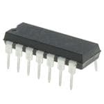
| 描述 | IC OPAMP CHOPPER 2MHZ 14DIP运算放大器 - 运放 Low VOS CMOS |
| 产品分类 | Linear - Amplifiers - Instrumentation, OP Amps, Buffer Amps集成电路 - IC |
| 品牌 | Microchip Technology |
| 产品手册 | |
| 产品图片 |
|
| rohs | 符合RoHS无铅 / 符合限制有害物质指令(RoHS)规范要求 |
| 产品系列 | 放大器 IC,运算放大器 - 运放,Microchip Technology TC7650CPD- |
| 数据手册 | http://www.microchip.com/mymicrochip/filehandler.aspx?ddocname=en011515 |
| 产品型号 | TC7650CPD |
| 产品目录页面 | |
| 产品种类 | 运算放大器 - 运放 |
| 供应商器件封装 | 14-PDIP |
| 共模抑制比—最小值 | 120 dB |
| 关闭 | No Shutdown |
| 包装 | 管件 |
| 压摆率 | 2.5 V/µs |
| 双重电源电压 | +/- 3 V, +/- 5 V |
| 商标 | Microchip Technology |
| 增益带宽生成 | 2 MHz |
| 增益带宽积 | 2MHz |
| 安装类型 | 通孔 |
| 安装风格 | Through Hole |
| 封装 | Tube |
| 封装/外壳 | 14-DIP(0.300",7.62mm) |
| 封装/箱体 | PDIP-14 |
| 工作温度 | 0°C ~ 70°C |
| 工作电源电压 | 4.5 V to 16 V, +/- 2.25 V to +/- 8 V |
| 工厂包装数量 | 30 |
| 技术 | CMOS |
| 放大器类型 | 断路器(零漂移) |
| 最大双重电源电压 | +/- 8 V |
| 最大工作温度 | + 70 C |
| 最小双重电源电压 | +/- 2.25 V |
| 最小工作温度 | 0 C |
| 标准包装 | 30 |
| 电压-电源,单/双 (±) | 4.5 V ~ 16 V, ±2.25 V ~ 8 V |
| 电压-输入失调 | 0.7µV |
| 电流-电源 | 2mA |
| 电流-输入偏置 | 1.5pA |
| 电流-输出/通道 | - |
| 电源电流 | 3.5 mA |
| 电路数 | 1 |
| 转换速度 | 2.5 V/us |
| 输入偏压电流—最大 | 10 pA |
| 输入补偿电压 | 5 uV |
| 输出类型 | - |
| 通道数量 | 1 Channel |


- 商务部:美国ITC正式对集成电路等产品启动337调查
- 曝三星4nm工艺存在良率问题 高通将骁龙8 Gen1或转产台积电
- 太阳诱电将投资9.5亿元在常州建新厂生产MLCC 预计2023年完工
- 英特尔发布欧洲新工厂建设计划 深化IDM 2.0 战略
- 台积电先进制程称霸业界 有大客户加持明年业绩稳了
- 达到5530亿美元!SIA预计今年全球半导体销售额将创下新高
- 英特尔拟将自动驾驶子公司Mobileye上市 估值或超500亿美元
- 三星加码芯片和SET,合并消费电子和移动部门,撤换高东真等 CEO
- 三星电子宣布重大人事变动 还合并消费电子和移动部门
- 海关总署:前11个月进口集成电路产品价值2.52万亿元 增长14.8%


PDF Datasheet 数据手册内容提取
TC7650 Chopper Stabilized Operational Amplifier Features Package Type • Low Input Offset Voltage: 0.7µV Typ 8-Pin DIP • Low Input Offset Voltage Drift: 0.05V/°C Max • Low Input Bias Current: 10pA Max CA 1 8 CB • High Impedance Differential CMOS Inputs: 1012 –INPUT 2 7 VDD • High Open Loop Voltage Gain: 120dB Min. • Low Input Noise Voltage: 2.0Vp-p +INPUT 3 TC7650CPA 6 OUTPUT • High Slew Rate: 2.5V/sec. VSS 4 5 OUTPUT CLAMP • Low Power Operation: 20mW • Output Clamp Speeds Recovery Time • Compensated Internally for Stable Unity Gain 14-Pin DIP Operation • Direct Replacement for ICL7650 CB 1 14 INT/EXT • Available in 8-Pin Plastic DIP and 14-Pin Plastic CA 2 13 EXT CLK IN DIP Packages NC 3 12 INT CLK OUT Applications –INPUT 4 TC7650CPD 11 VDD • Instrumentation +INPUT 5 10 OUTPUT • Medical Instrumentation • Embedded Control NC 6 9 OUTPUT CLAMP • Temperature Sensor Amplifier VSS 7 8 CRETN • Strain Gage Amplifier Device Selection Table NC = NO INTERNAL CONNECTION Part Temperature Package Max V Number Range OS TC7650CPA 8-Pin PDIP 0°C to +70°C 5V TC7650CPD 14-Pin PDIP 0°C to +70°C 5V 2001-2012 Microchip Technology Inc. DS21463C-page 1
TC7650 General Description The TC7650 nulling scheme corrects both DC V OS errors and V drift errors with temperature. A nulling The TC7650 CMOS chopper stabilized operational OS amplifier alternately corrects its own V errors and the amplifier practically removes offset voltage error terms OS main amplifier V error. Offset nulling voltages are from system error calculations. The 5V maximum V OS OS stored on two user supplied external capacitors. The specification, for example, represents a 15 times capacitors connect to the internal amplifier V null improvement over the industry standard OP07E. The OS points. The main amplifier input signal is never 50nV/°C offset drift specification is over 25 times lower switched. Switching spikes are not present at the than the OP07E. The increased performance elimi- TC7650 output. nates V trim procedures, periodic potentiometer OS adjustment and the reliability problems caused by dam- The 14-pin dual-in-line package (DIP) has an external aged trimmers. oscillator input to drive the nulling circuitry for optimum noise performance. Both the 8 and 14-pin DIPs have The TC7650 performance advantages are achieved an output voltage clamp circuit to minimize overload without the additional manufacturing complexity and recovery time. cost incurred with laser or "zener zap" V trim tech- OS niques. Functional Block Diagram Output 14-Pin DIP Only Clamp Output Clamp INT/EXT Circuit Oscillator EXT CLK IN CLK OUT Main Amplifier A B Inputs Output NULL CB Intermod Compensation B B B A CA Null Amplifier TC7650 A Null *CRETN *For 8-Pin DIP, connect to Vss DS21463C-page 2 2001-2012 Microchip Technology Inc.
TC7650 1.0 ELECTRICAL *Stresses above those listed under “Absolute Maximum Ratings” may cause permanent damage to the device. CHARACTERISTICS These are stress ratings only and functional operation of the device at these or any other conditions above those indi- ABSOLUTE MAXIMUM RATINGS* cated in the operation sections of the specifications is not implied. Exposure to Absolute Maximum Rating conditions Total Supply Voltage (V to V ).......................+18V DD SS for extended periods my affect device reliability. Input Voltage....................(V +0.3V) to (V – 0.3V) DD SS Storage Temperature Range..............-65°C to +150°C Voltage on Oscillator Control Pins...............V to V DD SS Duration of Output Short Circuit.....................Indefinite Current Into Any Pin............................................10mA While Operating (Note 3)............................100µA Package Power Dissipation (T 70°C) A 8-Pin Plastic DIP.......................................730mW 14-Pin Plastic DIP.....................................800mW Operating Temperature Range C Device..........................................0°C to +70°C TC7652 ELECTRICAL SPECIFICATIONS Electrical Characteristics: VDD = +5V, VSS = -5V, CA = CB = 0.1F, TA = +25°C, unless otherwise indicated. Symbol Parameter Min. Typ Max Units Test Conditions Input VOS Input Offset Voltage — ±0.7 ±5 — TA = +25°C — ±1.0 — V Over Operating Temp Range VOS/T Input Offset Voltage Average — 0.01 0.05 V/°C Operating Temperature Range Temperature Coefficient Offset Voltage vs. Time — 100 — nV/ month IBIAS Input Bias Current — 1.5 10 pA TA = +25°C — 35 150 pA 0°C TA +70°C — 100 400 pA -25°C TA +85°C IOS Input Offset Current — 0.5 — pA eNP-P Input Noise Voltage — 2 — VP-P RS = 100, 0 to 10Hz IN Input Noise Current — 0.01 — pA/Hz f = 10Hz RIN Input Resistance — 1012 CMVR Common Mode Voltage Range -5 -5.2 to +2 +1.6 V CMRR Common Mode Rejection Ratio 120 130 — dB CMVR = -5V to +1.5V Output A Large Signal Voltage Gain 120 130 — dB RL = 10k VOUT Output Voltage Swing (Note 2) ±4.7 ±4.85 — V RL = 10k — ±4.95 — V RL = 100k Clamp ON Current 25 70 200 A RL = 100k (Note 1) Clamp OFF Current — 1 — pA -4V < VOUT < +4V (Note 1) Dynamic BW Unity Gain Bandwidth — 2.0 — MHz Unity Gain (+1) SR Slew Rate — 2.5 — V/sec CL = 50pF, RL = 10k tR Rise Time — 0.2 — sec Overshoot — 20 — % fCH Internal Chopping Frequency 120 200 375 Hz Pins 12–14 Open (DIP) Supply VDD, VSS Operating Supply Range 4.5 — 16 V IS Supply Current — 2 3.5 mA No Load PSRR Power Supply Rejection Ratio 120 130 dB VS = ±3V to ±8V Note 1: See "Output Clamp" discussion. 2: Output clamp not connected. See typical characteristics curves for output swing versus clamp current characteristics. 3: Limiting input current to 100A is recommended to avoid latch-up problems. 2001-2012 Microchip Technology Inc. DS21463C-page 3
TC7650 2.0 PIN DESCRIPTIONS The descriptions of the pins are listed in Table 2-1. TABLE 2-1: PIN FUNCTION TABLE Pin Number Symbol Description 8-pin DIP 14-pin DIP 1,8 2,1 C , C Nulling capacitor pins A B 2 4 -INPUT Inverting Input 3 5 +INPUT Non-inverting Input 4 7 V Negative Power Supply SS 5 9 OUTPUT Output Voltage Clamp CLAMP 6 10 OUTPUT Output 7 11 V Positive Power Supply DD — 3,6 NC No internal connection — 8 C Capacitor current return pin RETN — 12 INT CLK OUT Internal Clock Output — 13 EXT CLK IN External Clock Input — 14 INT/EXT Select Internal or External Clock 3.0 DETAILED DESCRIPTION After the nulling amplifier is zeroed, the main amplifier is zeroed; the A switches open and B switches close. 3.1 Theory of Operation The output voltage equation is: Figure 3-1 shows the major elements of the TC7650. EQUATION 3-2: There are two amplifiers (the main amplifier and the nulling amplifier), and both have offset null capability. The main amplifier is connected full-time from the input V = A V + (V+ - V-) + A (V+ - V-) + A V OUT M OSM N N OSE to the output. The nulling amplifier, under the control of the chopping frequency oscillator and clock circuit, alternately nulls itself and the main amplifier. Two exter- EQUATION 3-3: nal capacitors provide the required storage of the null- ing potentials and the necessary nulling loop time + - VOSM+VOSN V = A A V –V +------------------------------------------- constants. The nulling arrangement operates over the OUT M N A N full common mode and power supply ranges, and is also independent of the output level, thus giving excep- As desired, the device offset voltages are reduced by tionally high CMRR, PSRR and A . VOL the high open loop gain of the nulling amplifier. Careful balancing of the input switches minimizes chopper frequency charge injection at the input termi- 3.2 Output Stage/Loading nals, and the feed forward type injection into the com- pensation capacitor that can cause output spikes in this The output circuit is a high impedance stage (approxi- type of circuit. mately 18k). With loads less than this, the chopper The circuit's offset voltage compensation is easily amplifier behaves in some ways like a trans-conduc- shown. With the nulling inputs shorted, a voltage tance amplifier whose open-loop gain is proportional to almost identical to the nulling amplifier offset voltage is load resistance. For example, the open loop gain will stored on C . The effective offset voltage at the null be 17dB lower with a 1k load than with a 10k load. A amplifier input is: If the amplifier is used strictly for DC, the lower gain is of little consequence, since the DC gain is typically greater than 120dB, even with a 1k load. In wideband EQUATION 3-1: applications, the best frequency response will be V = --------1----------V achieved with a load resistor of 10k or higher. This OSE A +1 OSN N results in a smooth 6dB/octave response from 0.1Hz to 2MHz, with phase shifts of less than 10° in the transi- DS21463C-page 4 2001-2012 Microchip Technology Inc.
TC7650 tion region, where the main amplifier takes over from ing sum and difference frequencies, and causing dis- the null amplifier. The clock frequency sets the transi- turbances to the gain and phase versus frequency tion region. characteristics near the chopping frequency. These effects are substantially reduced in the TC7650 by 3.3 Intermodulation feeding the nulling circuit with a dynamic current corre- sponding to the compensation capacitor current in such Previous chopper stabilized amplifiers have suffered a way as to cancel that portion of the input signal due from intermodulation effects between the chopper fre- to a finite AC gain. The intermodulation and gain/phase quency and input signals. These arise because the disturbances are held to very low values, and can gen- finite AC gain of the amplifier results in a small AC sig- erally be ignored. nal at the input. This is seen by the zeroing circuit as an error signal, which is chopped and fed back, thus inject- FIGURE 3-1: TC7650 CONTAINS A NULLING AND MAIN AMPLIFIER. OFFSET CORRECTION VOLTAGES ARE STORED ON TWO EXTERNAL CAPACITORS. V+ Main + Amplifier Analog Input Null VOUT - V- Gain = A M B TC7650 + B C B Null A - A Null C A Amplifier Gain = A , Offset = V N OSN FIGURE 3-2: NULLING CAPACITOR 3.5 Clock Operation CONNECTION The internal oscillator is set for a 200Hz nominal chop- VDD VSS VDD ping frequency on both the 8- and 14-pin DIPs. With the 14-pin DIP TC7650, the 200 Hz internal chopping fre- 4 11 2 7 quency is available at the internal clock output (Pin 12). - - 7 A 400Hz nominal signal will be present at the external 10 6 TC7650 TC7650 clock input pin (Pin 13) with INT/EXT high or open. This 5 + 1 3 + 4 is the internal clock signal before a divide-by-two oper- 8 CB ation. 8 2 1 VSS The 14-pin DIP device can be driven by an external clock. The INT/EXT input (Pin 14) has an internal pull- CA CB CA up and may be left open for internal clock operation. If an external clock is used, INT/EXT must be tied to V 14-PIN PACKAGE 8-PIN PACKAGE SS (Pin 7) to disable the internal clock. The external clock signal is applied to the external clock input (Pin 13). 3.4 Nulling Capacitor Connection The external clock amplitude should swing between The offset voltage correction capacitors are connected VDD and ground for power supplies up to ±6V and to C and C . The common capacitor connection is between V+ and V+ -6V for higher supply voltages. A B made to VSS (Pin 4) on the 8-pin packages and to At low frequencies the external clock duty cycle is not capacitor return (CRETN, Pin 8) on the 14-pin packages. critical, since an internal divide-by-two gives the The common connection should be made through a desired 50% switching duty cycle. The offset storage separate PC trace or wire to avoid voltage drops. The correction capacitors are charged only when the exter- capacitors outside foil, if possible, should be connected nal clock input is high. A 50% to 80% external clock to C or V . RETN SS 2001-2012 Microchip Technology Inc. DS21463C-page 5
TC7650 positive duty cycle is desired for frequencies above FIGURE 3-5: INVERTING AMPLIFIER WITH 500Hz to ensure transients settle before the internal OPTIONAL CLAMP switches open. R2 The external clock input can also be used as a strobe input. If a strobe signal is connected at the external Clamp clock input so that it is LOW during the time an overload R1 signal is applied, neither capacitor will be charged. The Input leakage currents at the capacitors pins are very low. At TC7650 C Output 25°C a typical TC7650 will drift less than 10V/sec. + R * C (R1 R2) ‡ 100 kΩ 3.6 Output Clamp For Full Clamp Effect Chopper-stabilized systems can show long recovery *Connect To VR– 0.1 µ F 0.1 µ F times from overloads. If the output is driven to either On 8-Pin DIP. supply rail, output saturation occurs. The inputs are no longer held at a "virtual ground." The V null circuit The output clamp circuit is shown in Figure 3-3, with OS treats the differential signal as an offset and tries to cor- typical inverting and non-inverting circuit connections rect it by charging the external capacitors. The nulling shown in Figures 3-4 and 3-5. Output voltage versus circuit also saturates. Once the input signal returns to clamp circuit current characteristics are shown in the normal, the response time is lengthened by the long typical operating curves. For the clamp to be fully effec- recovery time of the nulling amplifier and external tive, the impedance across the clamp output should be capacitors. greater than 100k. Through an external clamp connection, the TC7650 3.7 Latch-Up Avoidance eliminates the overload recovery problem by reducing the feedback network gain before the output voltage Junction-isolated CMOS circuits inherently include a reaches either supply rail. parasitic 4-layer (p-n-p-n) structure which has charac- teristics similar to an SCR. Under certain circum- FIGURE 3-3: INTERNAL CLAMP CIRCUIT stances this junction may be triggered into a low- Internal impedance state, resulting in excessive supply current. Positive Clamp Bias ≈ V+ - VT ≈ V+ - 0.7 To avoid this condition, no voltage greater than 0.3V P-Channel beyond the supply rails should be applied to any pin. In general, the amplifier supplies must be established Output either at the same time or before any input signals are Clamp Pin applied. If this is not possible, the drive circuits must N-Channel limit input current flow to under 0.1mA to avoid latch- up. 3.8 Thermoelectric Potentials FIGURE 3-4: NON-INVERTING AMPLIFIER WITH OPTIONAL CLAMP Precision DC measurements are ultimately limited by *Connect To VSS 0.1µF thermoelectric potentials developed in thermocouple On 8-Pin DIP. junctions of dissimilar metals, alloys, silicon, etc. Unless all junctions are at the same temperature, ther- C * moelectric voltages, typically around 0.1V/°C, but up Input + R to tens of V/°C for some materials, will be generated. TC7650C Output In order to realize the benefits extremely-low offset volt- R2 ages provide, it is essential to take special precautions Clamp to avoid temperature gradients. All components should be enclosed to eliminate air movement, especially R3 R3 + (R1/R2) ‡ 100 kΩ R1 ttehmos.e cLaouws edt hbeyr pmooweelerc dtrisics ipacotin-egf feicleiemnet ntcso innn theect sioynss- For Full Clamp Effect should be used where possible and power supply volt- ages and power dissipation should be kept to a mini- mum. High impedance loads are preferable, and separation from surrounding heat dissipating elements is advised. DS21463C-page 6 2001-2012 Microchip Technology Inc.
TC7650 3.9 Pin Compatibility FIGURE 3-6: INPUT GUARD CONNECTION On the 8-pin mini-DIP TC7650, the external null stor- Inverting Amplifier age capacitors are connected to pins 1 and 8. On most R1 R2 other operational amplifiers these are left open or are Input used for offset potentiometer or compensation capaci- tor connections. - For OP05 and OP07 operational amplifiers, the Output replacement of the offset null potentiometer between + pins 1 and 8 by two capacitors from the pins to V will SS convert the OP05/07 pin configurations for TC7650 R3* operation. For LM108 devices, the compensation capacitor is replaced by the external nulling capacitors. The LM101/748/709 pinouts are modified similarly by removing any circuit connections to Pin 5. On the Noninverting Amplifier TC7650, Pin 5 is the output clamp connection. Other operational amplifiers may use this pin as an off- R2 set or compensation point. The minor modifications needed to retrofit a TC7650 R3* - into existing sockets operating at reduced power sup- ply voltages make prototyping and circuit verification Output straightforward. + R1 3.10 Input Guarding High impedance, low leakage CMOS inputs allow the Input Should Be Low Impedence For TsoCu7r6ce5s0. tSot ramya kleea kmageea spuarethmse cnatsn oinfc rheigahse-i minppeudta cnucre- NOTE: R3 = R1 R2 Optimum Guarding R1 + R2 rents and decrease input resistance unless inputs are guarded. A guard is a conductive PC trace surrounding Follower the input terminals. The ring connects to a low imped- ance point at the same potential as the inputs. Stray leakages are absorbed by the low impedance ring. The R3* equal potential between ring and inputs prevents input leakage currents. Typical guard connections are shown - in Figure 3-6. Output The 14-pin DIP configuration has been specifically Input + designed to ease input guarding. The pins adjacent to the inputs are unused. In applications requiring low leakage currents, boards should be cleaned thoroughly and blown dry after sol- dering. Protective coatings will prevent future board contamination. 3.11 Component Selection The two required capacitors, C and C , have optimum A B values, depending on the clock or chopping frequency. For the preset internal clock, the correct value is 0.1F. To maintain the same relationship between the chop- ping frequency and the nulling time constant, the capacitor values should be scaled in proportion to the external clock, if used. High quality film type capacitors (such as Mylar) are preferred; ceramic or other lower grade capacitors may be suitable in some applications. For fast settling on initial turn-on, low dielectric absorp- tion capacitors (such as polypropylene) should be used. With ceramic capacitors, several seconds may be required to settle to 1V. 2001-2012 Microchip Technology Inc. DS21463C-page 7
TC7650 4.0 TYPICAL CHARACTERISTICS Note: The graphs and tables provided following this note are a statistical summary based on a limited number of samples and are provided for informational purposes only. The performance characteristics listed herein are not tested or guaranteed. In some graphs or tables, the data presented may be outside the specified operating range (e.g., outside specified power supply range) and therefore outside the warranted range. Positive Clamp Current Negative Clamp Current vs. Output Voltage vs. Output Voltage 1 mA 1 mA 0.1 mA TA = +25˚C 0.1 mA TA = +25˚C VS = ±5V VS = ±5V 0.01 mA 0.01 mA T 1m A T 1m A N N E E R 0.1m A R 0.1m A R R U U C 0.01m A C 0.01m A P P M M A 1 nA A 1 nA L L C C 0.1 nA 0.1 nA 0.01 nA 0.01 nA 1 pA 1 pA 4.0 4.1 4.2 4.3 4.4 4.5 4.6 4.7 4.8 4.9 5.0 -4.0 -4.1 -4.2 -4.3 -4.4 -4.5 -4.6 -4.7 -4.8-4.9 -5.0 OUTPUT VOLTAGE (V) OUTPUT VOLTAGE (V) Supply Current vs. Gain/Phase vs. Frequency Supply Voltage 3.0 30 225 TA = +25˚C 20 180 A) 2.6 10 135 m RRENT ( 2.2 N (dB) –100 GAIN 9405 E (deg) LY CU 1.8 GAI ––3200 PHASE 0-45 PHAS P P SU 1.4 –40 -90 –50 CLOSED-LOOP -135 GAIN = 20 1.0 –60 -180 5 6 7 8 9 10 11 12 13 14 15 1k 10k 100k 1M 10M SUPPLY VOLTAGE (V) FREQUENCY (H z ) DS21463C-page 8 2001-2012 Microchip Technology Inc.
TC7650 5.0 PACKAGING INFORMATION 5.1 Package Marking Information Package marking information not available at this time. 5.2 Package Dimensions Note: For the most current package drawings, please see the Microchip Packaging Specification located at http://www.microchip.com/packaging 8-Pin Plastic DIP PIN 1 .260 (6.60) .240 (6.10) .045 (1.14) .070 (1.78) .030 (0.76) .040 (1.02) .310 (7.87) .400 (10.16) .290 (7.37) .348 (8.84) .200 (5.08) .140 (3.56) .040 (1.02) .020 (0.51) .015 (0.38) 3˚MIN. .150 (3.81) .008 (0.20) .115 (2.92) .400 (10.16) .310 (7.87) .110 (2.79) .022 (0.56) .090 (2.29) .015 (0.38) Dimensions: inches (mm) Note: For the most current package drawings, please see the Microchip Packaging Specification located at http://www.microchip.com/packaging 14-Pin PDIP (Narrow) PIN 1 .260 (6.60) .240 (6.10) .310 (7.87) .770 (19.56) .290 (7.37) .745 (18.92) .200 (5.08) .140 (3.56) .040 (1.02) .150 (3.81) .020 (0.51) ..001058 ((00..3280)) 3˚MIN. .115 (2.92) .400 (10.16) .310 (7.87) .110 (2.79) .070 (1.78) .022 (0.56) .090 (2.29) .045 (1.14) .015 (0.38) Dimensions: inches (mm) 2001-2012 Microchip Technology Inc. DS21463C-page 9
TC7650 6.0 REVISION HISTORY Revision C (December 2012) Added a note to each package outline drawing. DS21463C-page 10 2001-2012 Microchip Technology Inc.
TC7650 SALES AND SUPPORT Data Sheets Products supported by a preliminary Data Sheet may have an errata sheet describing minor operational differences and recommended workarounds. To determine if an errata sheet exists for a particular device, please contact one of the following: 1. Your local Microchip sales office 2. The Microchip Worldwide Site (www.microchip.com) Please specify which device, revision of silicon and Data Sheet (include Literature #) you are using. New Customer Notification System Register on our web site (www.microchip.com/cn) to receive the most current information on our products. 2001-2012 Microchip Technology Inc. DS21463C-page 11
TC7650 NOTES: DS21463C-page 12 2001-2012 Microchip Technology Inc.
Note the following details of the code protection feature on Microchip devices: • Microchip products meet the specification contained in their particular Microchip Data Sheet. • Microchip believes that its family of products is one of the most secure families of its kind on the market today, when used in the intended manner and under normal conditions. • There are dishonest and possibly illegal methods used to breach the code protection feature. All of these methods, to our knowledge, require using the Microchip products in a manner outside the operating specifications contained in Microchip’s Data Sheets. Most likely, the person doing so is engaged in theft of intellectual property. • Microchip is willing to work with the customer who is concerned about the integrity of their code. • Neither Microchip nor any other semiconductor manufacturer can guarantee the security of their code. Code protection does not mean that we are guaranteeing the product as “unbreakable.” Code protection is constantly evolving. We at Microchip are committed to continuously improving the code protection features of our products. Attempts to break Microchip’s code protection feature may be a violation of the Digital Millennium Copyright Act. If such acts allow unauthorized access to your software or other copyrighted work, you may have a right to sue for relief under that Act. Information contained in this publication regarding device Trademarks applications and the like is provided only for your convenience The Microchip name and logo, the Microchip logo, dsPIC, and may be superseded by updates. It is your responsibility to FlashFlex, KEELOQ, KEELOQ logo, MPLAB, PIC, PICmicro, ensure that your application meets with your specifications. PICSTART, PIC32 logo, rfPIC, SST, SST Logo, SuperFlash MICROCHIP MAKES NO REPRESENTATIONS OR and UNI/O are registered trademarks of Microchip Technology WARRANTIES OF ANY KIND WHETHER EXPRESS OR Incorporated in the U.S.A. and other countries. IMPLIED, WRITTEN OR ORAL, STATUTORY OR OTHERWISE, RELATED TO THE INFORMATION, FilterLab, Hampshire, HI-TECH C, Linear Active Thermistor, INCLUDING BUT NOT LIMITED TO ITS CONDITION, MTP, SEEVAL and The Embedded Control Solutions QUALITY, PERFORMANCE, MERCHANTABILITY OR Company are registered trademarks of Microchip Technology FITNESS FOR PURPOSE. Microchip disclaims all liability Incorporated in the U.S.A. arising from this information and its use. Use of Microchip Silicon Storage Technology is a registered trademark of devices in life support and/or safety applications is entirely at Microchip Technology Inc. in other countries. the buyer’s risk, and the buyer agrees to defend, indemnify and Analog-for-the-Digital Age, Application Maestro, BodyCom, hold harmless Microchip from any and all damages, claims, chipKIT, chipKIT logo, CodeGuard, dsPICDEM, suits, or expenses resulting from such use. No licenses are dsPICDEM.net, dsPICworks, dsSPEAK, ECAN, conveyed, implicitly or otherwise, under any Microchip ECONOMONITOR, FanSense, HI-TIDE, In-Circuit Serial intellectual property rights. Programming, ICSP, Mindi, MiWi, MPASM, MPF, MPLAB Certified logo, MPLIB, MPLINK, mTouch, Omniscient Code Generation, PICC, PICC-18, PICDEM, PICDEM.net, PICkit, PICtail, REAL ICE, rfLAB, Select Mode, SQI, Serial Quad I/O, Total Endurance, TSHARC, UniWinDriver, WiperLock, ZENA and Z-Scale are trademarks of Microchip Technology Incorporated in the U.S.A. and other countries. SQTP is a service mark of Microchip Technology Incorporated in the U.S.A. GestIC and ULPP are registered trademarks of Microchip Technology Germany II GmbH & Co. & KG, a subsidiary of Microchip Technology Inc., in other countries. All other trademarks mentioned herein are property of their respective companies. © 2001-2012, Microchip Technology Incorporated, Printed in the U.S.A., All Rights Reserved. Printed on recycled paper. ISBN: 9781620768402 QUALITY MANAGEMENT SYSTEM Microchip received ISO/TS-16949:2009 certification for its worldwide headquarters, design and wafer fabrication facilities in Chandler and CERTIFIED BY DNV Tempe, Arizona; Gresham, Oregon and design centers in California and India. The Company’s quality system processes and procedures == ISO/TS 16949 == are for its PIC® MCUs and dsPIC® DSCs, KEELOQ® code hopping devices, Serial EEPROMs, microperipherals, nonvolatile memory and analog products. In addition, Microchip’s quality system for the design and manufacture of development systems is ISO 9001:2000 certified. 2001-2012 Microchip Technology Inc. DS21463C-page 13
Worldwide Sales and Service AMERICAS ASIA/PACIFIC ASIA/PACIFIC EUROPE Corporate Office Asia Pacific Office India - Bangalore Austria - Wels 2355 West Chandler Blvd. Suites 3707-14, 37th Floor Tel: 91-80-3090-4444 Tel: 43-7242-2244-39 Chandler, AZ 85224-6199 Tower 6, The Gateway Fax: 91-80-3090-4123 Fax: 43-7242-2244-393 Tel: 480-792-7200 Harbour City, Kowloon India - New Delhi Denmark - Copenhagen Fax: 480-792-7277 Hong Kong Tel: 91-11-4160-8631 Tel: 45-4450-2828 Technical Support: Tel: 852-2401-1200 Fax: 91-11-4160-8632 Fax: 45-4485-2829 http://www.microchip.com/ support Fax: 852-2401-3431 India - Pune France - Paris Web Address: Australia - Sydney Tel: 91-20-2566-1512 Tel: 33-1-69-53-63-20 www.microchip.com Tel: 61-2-9868-6733 Fax: 91-20-2566-1513 Fax: 33-1-69-30-90-79 Atlanta Fax: 61-2-9868-6755 Japan - Osaka Germany - Munich Duluth, GA China - Beijing Tel: 81-6-6152-7160 Tel: 49-89-627-144-0 Tel: 86-10-8569-7000 Fax: 49-89-627-144-44 Tel: 678-957-9614 Fax: 81-6-6152-9310 Fax: 678-957-1455 Fax: 86-10-8528-2104 Japan - Tokyo Italy - Milan China - Chengdu Tel: 39-0331-742611 Boston Tel: 81-3-6880- 3770 Tel: 86-28-8665-5511 Fax: 39-0331-466781 Westborough, MA Fax: 81-3-6880-3771 Tel: 774-760-0087 Fax: 86-28-8665-7889 Korea - Daegu Netherlands - Drunen Fax: 774-760-0088 China - Chongqing Tel: 82-53-744-4301 Tel: 31-416-690399 Chicago Tel: 86-23-8980-9588 Fax: 82-53-744-4302 Fax: 31-416-690340 Itasca, IL Fax: 86-23-8980-9500 Korea - Seoul Spain - Madrid Tel: 630-285-0071 China - Hangzhou Tel: 82-2-554-7200 Tel: 34-91-708-08-90 Fax: 630-285-0075 Tel: 86-571-2819-3187 Fax: 82-2-558-5932 or Fax: 34-91-708-08-91 Cleveland Fax: 86-571-2819-3189 82-2-558-5934 UK - Wokingham Independence, OH China - Hong Kong SAR Malaysia - Kuala Lumpur Tel: 44-118-921-5869 Tel: 216-447-0464 Tel: 852-2943-5100 Tel: 60-3-6201-9857 Fax: 44-118-921-5820 Fax: 216-447-0643 Fax: 852-2401-3431 Fax: 60-3-6201-9859 Dallas China - Nanjing Malaysia - Penang Addison, TX Tel: 86-25-8473-2460 Tel: 60-4-227-8870 Tel: 972-818-7423 Fax: 86-25-8473-2470 Fax: 60-4-227-4068 Fax: 972-818-2924 China - Qingdao Philippines - Manila Detroit Tel: 86-532-8502-7355 Tel: 63-2-634-9065 Farmington Hills, MI Fax: 86-532-8502-7205 Fax: 63-2-634-9069 Tel: 248-538-2250 Fax: 248-538-2260 China - Shanghai Singapore Tel: 86-21-5407-5533 Tel: 65-6334-8870 Indianapolis Fax: 86-21-5407-5066 Fax: 65-6334-8850 Noblesville, IN Tel: 317-773-8323 China - Shenyang Taiwan - Hsin Chu Fax: 317-773-5453 Tel: 86-24-2334-2829 Tel: 886-3-5778-366 Fax: 86-24-2334-2393 Fax: 886-3-5770-955 Los Angeles Mission Viejo, CA China - Shenzhen Taiwan - Kaohsiung Tel: 949-462-9523 Tel: 86-755-8864-2200 Tel: 886-7-213-7828 Fax: 949-462-9608 Fax: 86-755-8203-1760 Fax: 886-7-330-9305 Santa Clara China - Wuhan Taiwan - Taipei Santa Clara, CA Tel: 86-27-5980-5300 Tel: 886-2-2508-8600 Tel: 408-961-6444 Fax: 86-27-5980-5118 Fax: 886-2-2508-0102 Fax: 408-961-6445 China - Xian Thailand - Bangkok Toronto Tel: 86-29-8833-7252 Tel: 66-2-694-1351 Mississauga, Ontario, Fax: 86-29-8833-7256 Fax: 66-2-694-1350 Canada China - Xiamen Tel: 905-673-0699 Tel: 86-592-2388138 Fax: 905-673-6509 Fax: 86-592-2388130 China - Zhuhai Tel: 86-756-3210040 11/29/12 Fax: 86-756-3210049 DS21463C-page 14 2001-2012 Microchip Technology Inc.
Mouser Electronics Authorized Distributor Click to View Pricing, Inventory, Delivery & Lifecycle Information: M icrochip: TC7650CPA TC7650CPD