ICGOO在线商城 > 集成电路(IC) > 数据采集 - ADCs/DAC - 专用型 > AD9823KRUZ
 Datasheet下载
- 型号: AD9823KRUZ
- 制造商: Analog
- 库位|库存: xxxx|xxxx
- 要求:
| 数量阶梯 | 香港交货 | 国内含税 |
| +xxxx | $xxxx | ¥xxxx |
查看当月历史价格
查看今年历史价格
AD9823KRUZ产品简介:
ICGOO电子元器件商城为您提供AD9823KRUZ由Analog设计生产,在icgoo商城现货销售,并且可以通过原厂、代理商等渠道进行代购。 AD9823KRUZ价格参考¥26.56-¥55.64。AnalogAD9823KRUZ封装/规格:数据采集 - ADCs/DAC - 专用型, CDS (Correlated Double Sampler) 40M 14-TSSOP。您可以下载AD9823KRUZ参考资料、Datasheet数据手册功能说明书,资料中有AD9823KRUZ 详细功能的应用电路图电压和使用方法及教程。
AD9823KRUZ 是 Analog Devices Inc.(亚德诺半导体公司)生产的一款专用型数据采集器件,主要应用于图像处理领域,特别是高性能摄像和扫描设备中。该芯片集成了12位模数转换器(ADC)和相关双采样(CDS)电路,适用于需要高精度信号处理的场合。

其主要应用场景包括:

1. 工业相机与机器视觉:AD9823KRUZ适用于工业检测、自动化视觉系统,提供高精度图像信号采集,有助于提高图像质量和系统稳定性。

2. 医疗成像设备:如X光、超声波成像系统等,该芯片的高精度和低噪声特性有助于提升图像清晰度和诊断准确性。

3. 高端扫描仪与摄影设备:用于扫描仪或专业摄影设备中,实现高质量图像信号的采集与处理。

4. 安防监控系统:在高清视频监控系统中,AD9823KRUZ可提升图像采集性能,满足复杂环境下的清晰成像需求。

综上,AD9823KRUZ主要应用于对图像质量要求较高的专业领域,具备良好的动态性能和抗噪声能力,适合需要高精度模拟信号数字化处理的场景。
| 参数 | 数值 |
| ADC输入端数量 | 2 |
| 产品目录 | 集成电路 (IC)半导体 |
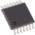
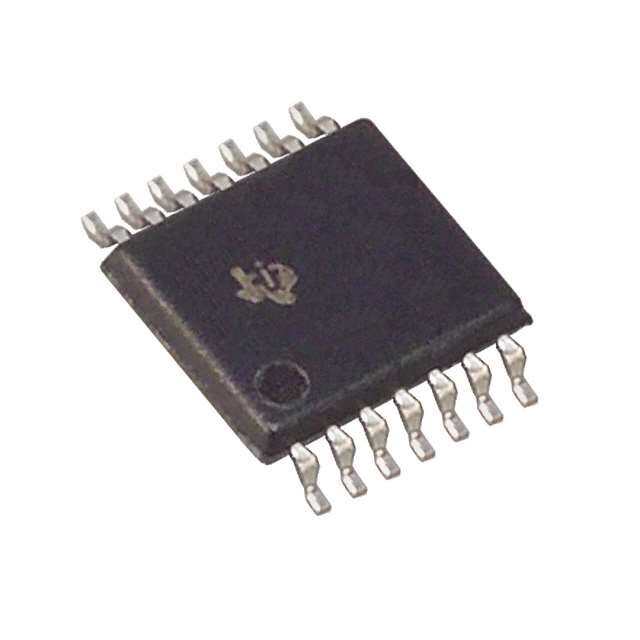
| 描述 | IC CDS FOR DGTL CAMERA 14-TSSOP视频模拟/数字化转换器集成电路 Correlated Double Sampler |
| 产品分类 | |
| 品牌 | Analog Devices |
| 产品手册 | |
| 产品图片 |
|
| rohs | 符合RoHS无铅 / 符合限制有害物质指令(RoHS)规范要求 |
| 产品系列 | 数据转换器IC,视频模拟/数字化转换器集成电路,Analog Devices AD9823KRUZ- |
| 数据手册 | |
| 产品型号 | AD9823KRUZ |
| 产品目录页面 | |
| 产品种类 | 视频模拟/数字化转换器集成电路 |
| 供应商器件封装 | 14-TSSOP |
| 分辨率 | 12 bit |
| 分辨率(位) | - |
| 功耗 | 50 mW |
| 包装 | 管件 |
| 商标 | Analog Devices |
| 安装类型 | 表面贴装 |
| 安装风格 | SMD/SMT |
| 封装 | Tube |
| 封装/外壳 | 14-TSSOP(0.173",4.40mm 宽) |
| 封装/箱体 | TSSOP-14 |
| 工作温度 | -25°C ~ 85°C |
| 工厂包装数量 | 96 |
| 接口类型 | CCD |
| 数据接口 | - |
| 最大功率耗散 | 50 mW |
| 最大工作温度 | + 85 C |
| 最小工作温度 | - 25 C |
| 标准包装 | 96 |
| 电压-电源 | 2.7 V ~ 3.6 V |
| 电压参考 | 0.5 V |
| 电压源 | 单电源 |
| 电源电压-最大 | 3.6 V |
| 电源电压-最小 | 2.7 V |
| 类型 | CDS - 关联双倍取样器 |
| 系列 | AD9823 |
| 转换器数量 | 2 |
| 转换速率 | 40 MS/s |
| 输入信号类型 | Single Ended |
| 输入电压 | 850 mV |
| 采样和保持 | No |
| 采样率(每秒) | 40M |


- 商务部:美国ITC正式对集成电路等产品启动337调查
- 曝三星4nm工艺存在良率问题 高通将骁龙8 Gen1或转产台积电
- 太阳诱电将投资9.5亿元在常州建新厂生产MLCC 预计2023年完工
- 英特尔发布欧洲新工厂建设计划 深化IDM 2.0 战略
- 台积电先进制程称霸业界 有大客户加持明年业绩稳了
- 达到5530亿美元!SIA预计今年全球半导体销售额将创下新高
- 英特尔拟将自动驾驶子公司Mobileye上市 估值或超500亿美元
- 三星加码芯片和SET,合并消费电子和移动部门,撤换高东真等 CEO
- 三星电子宣布重大人事变动 还合并消费电子和移动部门
- 海关总署:前11个月进口集成电路产品价值2.52万亿元 增长14.8%


PDF Datasheet 数据手册内容提取
Correlated Double Sampler (CDS) AD9823 FEATURES FUNCTIONAL BLOCK DIAGRAM 40 MHz correlated double sampler (CDS) Fixed 3.5 dB CDS gain AD9823 Low noise optical black clamp circuit 3.5dB FIXED GAIN 3 V single-supply operation OUTPUT 14-lead TSSOP package CCDIN CDS BUFFER OUTPUT APPLICATIONS BYP2 CLP Digital still cameras Digital video camcorders CLP CCTV cameras OUTPUT REFOUT BUFFER PC cameras Portable CCD imaging devices VDD INTERNAL INTERNAL TIMING REFERENCE GND SHP SHD BYP1 BYP3 04538-0-001 Figure 1. Functional Block Diagram PRODUCT DESCRIPTION The AD9823 is a correlated double sampler for digital camera The AD9823 is ideal for applications that need to place the CDS applications. It features a 40 MHz CDS amplifier with 3.5 dB of and VGA/ADC circuits on separate PC boards. The “pseudo fixed gain, an internal voltage reference supply, and timing differential” outputs of the AD9823 provide good signal control for the SHP and SHD sampling clocks. Output buffers integrity when interfaced with the differential input AD9821. are also included, providing drive strength for PCB traces and The AD9823 operates from a single 3 V power supply, typically direct connection to an image signal processor such as the dissipates 50 mW, and is packaged in a 14-lead TSSOP package. AD9821. Rev. 0 Information furnished by Analog Devices is believed to be accurate and reliable. However, no responsibility is assumed by Analog Devices for its use, nor for any infringements of patents or other rights of third parties that may result from its use. One Technology Way, P.O. Box 9106, Norwood, MA 02062-9106, U.S.A. Specifications subject to change without notice. No license is granted by implication or otherwise under any patent or patent rights of Analog Devices. Trademarks and Tel: 781.329.4700 www.analog.com registered trademarks are the property of their respective owners. Fax: 781.326.8703 © 2003 Analog Devices, Inc. All rights reserved.
AD9823 TABLE OF CONTENTS Specifications.....................................................................................3 Thermal Characteristics...............................................................5 General Specifications.................................................................3 ESD Caution...................................................................................5 Analog Specifications...................................................................3 Pin Configuration and Function Descriptions..............................6 Digital Specifications...................................................................3 SHP and SHD Timing..................................................................6 Timing Specifications..................................................................4 Outline Dimensions..........................................................................8 Absolute Maximum Ratings............................................................5 Ordering Guide.............................................................................8 REVISION HISTORY Revision 0: Initial Version Rev. 0 | Page 2 of 8
AD9823 SPECIFICATIONS GENERAL SPECIFICATIONS Table 1. Parameter Min Typ Max Unit Temperature Range Operating –25 +85 °C Storage –65 +150 °C Power Supply Voltage 2.7 3.6 V Power Consumption: f = 40 MHz, VDD = 3.0 V 50 mW SAMP Maximum Clock Rate 40 MHz Minimum Clock Rate 5 MHz ANALOG SPECIFICATIONS Table 2. T to T , VDD = 3.0 V, f = 40 MHz, unless otherwise noted. MIN MAX SAMP Parameter Min Typ Max Unit Notes Analog Input (CCDIN) Max Input Range Before Saturation1 850 mV p-p Allowable CCD Reset Transient1 500 mV Max CCD Black Pixel Amplitude1 100 mV Gain 2.5 3.5 4.5 dB Nonlinearity, 500 mV Input 1.0 % Max deviation from ideal straight line Input Referred Noise 100 µV rms Output noise divided by 3.5 dB gain Clamp Time Constant 190 µsec 0.1 µF BYP2 capacitor (proportional to capacitor value) Analog Outputs Typical Data Out Signal Range 0.5 1.5 V 0.5 V corresponds to black level REFOUT Voltage Level 0.5 V Fixed dc reference for signal output 1 Input signal characteristics defined as follows: 500mV TYP RESET TRANSIENT OPTIC1A0L0 mBLVA TCYKP PIXEINLPUT8 5S0IGmNVA TLY RPANGE 04538-0-002 All specifications subject to change without notice. DIGITAL SPECIFICATIONS Table 3. Parameter Symbol Min Typ Max Unit Logic Inputs (SHP, SHD, CLP) High Level Input Voltage V 2.1 V IH Low Level Input Voltage V 0.6 V IL High Level Input Current I 10 µA IH Low Level Input Current I 10 µA IL Input Capacitance C 10 pF IN Rev. 0 | Page 3 of 8
AD9823 TIMING SPECIFICATIONS Table 4. T to T , VDD = 3.0 V, f = 40 MHz, unless otherwise noted. MIN MAX SAMP Parameter (See Figure 3) Symbol Min Typ Max Unit Sample Clocks SHP, SHD Clock Period t 25 ns CP SHP Pulse Width t 5 6.25 ns SHP SHD Pulse Width t 5 6.25 ns SHD CLP Pulse Width1 t 4 10 pixels COB SHP Rising Edge to SHD Rising Edge t 12.0 12.5 ns S1 SHD Rising Edge to SHP Rising Edge t 12.0 12.5 ns S2 Internal Clock Delay t 3.0 ns ID Recommended Data CLK Timing (for AD9821) t 4.5 ns REC 1 Minimum CLP pulse width is for functional operation only. Wider typical pulses are recommended to achieve low noise clamp performance. Specifications subject to change without notice. Rev. 0 | Page 4 of 8
AD9823 ABSOLUTE MAXIMUM RATINGS Table 5. Parameter With Respect To Min Max Unit VDD GND −0.3 3.9 V SHP, SHD GND −0.3 VDD + 0.3 V BYP1, BYP2, BYP3 GND −0.3 VDD + 0.3 V CCDIN GND −0.3 VDD + 0.3 V DATAOUT, REFOUT GND −0.3 VDD + 0.3 V CLP GND −0.3 VDD + 0.3 V Junction Temperature 150 °C Lead Temperature (10 sec) 350 °C THERMAL CHARACTERISTICS Thermal Resistance 14-Pin, TSSOP Package θ = 89.2°C/W JA ESD CAUTION ESD (electrostatic discharge) sensitive device. Electrostatic charges as high as 4000 V readily accumulate on the human body and test equipment and can discharge without detection. Although this product features proprietary ESD protection circuitry, permanent damage may occur on devices subjected to high energy electrostatic discharges. Therefore, proper ESD precautions are recommended to avoid performance degradation or loss of functionality. Rev. 0 | Page 5 of 8
AD9823 PIN CONFIGURATION AND FUNCTION DESCRIPTIONS CLP 1 14 SHP NC 2 13 SHD VDD 3 AD9823 12 GND REFOUT 4 (NToOt Pto V SIEcaWle)11 CCDIN DATAOUT 5 10 NC BGYNPD1 67 98 BBYYPP32 04538-0-003 NC = NO CONNECT Figure 2. Pin Configurations Table 6. Pin Function Descriptions Pin Number Name Type1 Description 1 CLP DI Input Clamp Clock Input (active low, not latched internally). 2 NC NC No connection should be connected to GND or VDD. 3 VDD P Analog Supply. 4 REFOUT AO Output Reference Level. 5 DATAOUT AO Output Data Signal. 6 GND P Analog Ground. 7 BYP1 AO Internal Bias Level Decoupling. 8 BYP2 AO Internal Bias Level Decoupling. 9 BYP3 AO Internal Bias Level Decoupling. 10 NC NC No connection should be connected to GND or VDD. 11 CCDIN AI CCD Input. 12 GND P Analog Ground. 13 SHD DI CDS Sampling Clock Input (For CCD Data Level). 14 SHP DI CDS Sampling Clock Input (For CCD Ref Level). 1AI = Analog Input, AO = Analog Output, DI = Digital Input, DO = Digital Output, P = Power, NC = No Connect. SHP AND SHD TIMING CCD SIGNAL N N+1 N+2 N+9 N+10 t ID t ID t CP SHP tSHD tSHP tS1 tS2 SHD DATAOUT DATACLK (FOR AD9821) tREC 04538-0-004 Figure 3. SHP and SHD Timing Rev. 0 | Page 6 of 8
AD9823 HORIZONTAL EFFECTIVE PIXELS OPTICALBLACKPIXELS BLANKING DUMMY PIXELS EFFECTIVE PIXELS CCD SIGNAL CLP 04538-0-007 Figure 4. CLP Timing 3V ANALOG SUPPLY 4.7µF 0.1µF CLP SHP CLP 1 14 SHP NC SHD 2 13 SHD VDD 3 AD9823 12 GND (CONNECT TO VIN– ONR EADF9O8U21T) REFOUT 4 TOP VIEW 11 CCDIN 0.1µF CCDIN DATAOUT DATAOUT 5 (Not to Scale) 10 NC (CONNECT TO VIN+ ON AD9821) GND BYP3 6 9 BYP1 BYP2 7 8 0.1µF NC = NO CONNECT 0.1µF 0.1µF 04538-0-005 Figure 5. AD9823 Circuit Configuration 3V ANALOG SUPPLY 0.1µF 1.0µF SERIAL 3 1.0µF INTERFACE A 2 T Y SD KA B SDBT CCCDLTCVVRRC 3V 3V NNSSSSNDDVVN ANALOG SUPPLY ANALOG SUPPLY 484746454443424140393837 CLP DDD012 123 PIDINE N1TIFIER 333654TATEEVSSSTTS 0.1µF 4.7µF 0.1µF CLP 1 14SHP SSHHDP D3 4 33AVDD2 0.1µF NC 2 13SHD DD45 56 AD9821 3321BVIYNP–1 IMAGER INPUT, NEGATIVE REFVODUDT 34 ATODP9 V8IE2W3 1121GCCNDDIN 0.1µF OFRUOTPMUT DDDD678917890 (NToOtP to V SIEcWale 32220987VTTAEEIVNSSD+TTD1 IMAGER INPUT, POSITIVE DATABGOYNUPDT1 567(Not to Scale)1890NBB0.CYY1PPµF32 0.1µF CCD D1011 26AVSS 3V 0.1µF (MSB) D1112 25AVSS ANALOG SUPPLY DATA 12 131415161718192021222324 0.1µF 4.7µF OUTPUTS DSSK1CKBTTTC DSSLDNLOSSSN DRVDRVDVTACDVD PBCLPTETETE 3V A DRIVER D NC = INTERNALLY NOT CONNECTED SUPPLY 0.1µF 3 CLOCK INPUTS A0N.A1µLFOG3V SUPPLY 04538-0-006 Figure 6. Circuit Configuration with the AD9821 12-Bit Image Signal Processor Rev. 0 | Page 7 of 8
AD9823 OUTLINE DIMENSIONS 5.10 5.00 4.90 14 8 4.50 6.40 4.40 BSC 4.30 1 7 PIN 1 1.05 0.65 1.00 BSC 0.80 1.20 0.20 MAX 0.09 0.75 00..1055 00..3109 SPELAANTIENG COPLANARITY80°° 00..6405 0.10 COMPLIANT TO JEDEC STANDARDSMO-153AB-1 Figure 7. 14-Lead Thin Shrink Small Outline Package [TSSOP] (RU-14) Dimensions shown in millimeters ORDERING GUIDE Model Temperature Range Package Description Package Option AD9823BRUZ1 –25°C to +85°C TSSOP RU-14 1Z = Pb-free part. © 2003 Analog Devices, Inc. All rights reserved. Trademarks and registered trademarks are the property of their respective owners.. C04538-0-11/03(0) Rev. 0 | Page 8 of 8