ICGOO在线商城 > 集成电路(IC) > 数据采集 - 数模转换器 > AD9709ASTZ
 Datasheet下载
- 型号: AD9709ASTZ
- 制造商: Analog
- 库位|库存: xxxx|xxxx
- 要求:
| 数量阶梯 | 香港交货 | 国内含税 |
| +xxxx | $xxxx | ¥xxxx |
查看当月历史价格
查看今年历史价格
AD9709ASTZ产品简介:
ICGOO电子元器件商城为您提供AD9709ASTZ由Analog设计生产,在icgoo商城现货销售,并且可以通过原厂、代理商等渠道进行代购。 AD9709ASTZ价格参考¥65.20-¥101.45。AnalogAD9709ASTZ封装/规格:数据采集 - 数模转换器, 8 位 数模转换器 2 48-LQFP(7x7)。您可以下载AD9709ASTZ参考资料、Datasheet数据手册功能说明书,资料中有AD9709ASTZ 详细功能的应用电路图电压和使用方法及教程。
AD9709ASTZ 是由 Analog Devices Inc.(亚德诺半导体公司)生产的一款高性能 12 位数模转换器(DAC),属于数据采集 - 数模转换器类别。该型号具有以下应用场景:

 1. 通信系统
   - AD9709ASTZ 可用于无线通信系统中的信号生成,例如基站、中继器和调制解调器。其高分辨率和快速转换速度使其适合生成复杂的射频(RF)和中频(IF)信号。
   - 在软件定义无线电(SDR)系统中,该 DAC 可以生成可编程的波形,支持多种调制方式。

 2. 测试与测量设备
   - 在示波器、信号发生器和频谱分析仪等测试设备中,AD9709ASTZ 能够生成精确的模拟信号,用于校准或测试其他电子设备。
   - 其低失真和高线性度特性确保了测试结果的准确性。

 3. 工业自动化
   - 在工业控制系统中,AD9709ASTZ 可用于将数字控制信号转换为模拟信号,驱动执行器(如电机、阀门等)。
   - 它适用于需要高精度控制的应用场景,例如机器人控制、过程控制和运动控制。

 4. 医疗设备
   - 在医疗成像设备(如超声波、CT 和 MRI)中,AD9709ASTZ 可用于生成激励信号或处理重建图像所需的模拟信号。
   - 其稳定性和可靠性对于医疗应用至关重要。

 5. 音频处理
   - 该 DAC 可用于高质量音频设备中,将数字音频信号转换为模拟信号输出,适用于专业音响设备、家庭影院系统和录音设备。

 6. 雷达与导航系统
   - 在雷达和导航系统中,AD9709ASTZ 可用于生成脉冲信号或调制信号,支持目标检测和定位功能。

 总结
AD9709ASTZ 的主要优势在于其高分辨率、快速转换速度和低失真性能,这使得它在需要高精度和实时响应的应用中表现出色。无论是通信、工业还是医疗领域,这款 DAC 都能提供可靠的数模转换解决方案。
| 参数 | 数值 |
| 产品目录 | 集成电路 (IC)半导体 |
| 描述 | IC DAC 8BIT DUAL 125MSPS 48-LQFP数模转换器- DAC 8-Bit 125 MSPS Dual |
| DevelopmentKit | AD9709-EBZ |
| 产品分类 | |
| 品牌 | Analog Devices |
| 产品手册 | |
| 产品图片 |
|
| rohs | 符合RoHS无铅 / 符合限制有害物质指令(RoHS)规范要求 |
| 产品系列 | 数据转换器IC,数模转换器- DAC,Analog Devices AD9709ASTZTxDAC+® |
| 数据手册 | |
| 产品型号 | AD9709ASTZ |
| 产品培训模块 | http://www.digikey.cn/PTM/IndividualPTM.page?site=cn&lang=zhs&ptm=19145http://www.digikey.cn/PTM/IndividualPTM.page?site=cn&lang=zhs&ptm=18614http://www.digikey.cn/PTM/IndividualPTM.page?site=cn&lang=zhs&ptm=26125http://www.digikey.cn/PTM/IndividualPTM.page?site=cn&lang=zhs&ptm=26140http://www.digikey.cn/PTM/IndividualPTM.page?site=cn&lang=zhs&ptm=26150http://www.digikey.cn/PTM/IndividualPTM.page?site=cn&lang=zhs&ptm=26147 |
| 产品目录页面 | |
| 产品种类 | 数模转换器- DAC |
| 位数 | 8 |
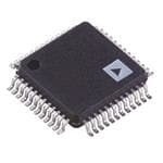
| 供应商器件封装 | 48-LQFP(7x7) |
| 分辨率 | 8 bit |
| 包装 | 托盘 |
| 商标 | Analog Devices |
| 安装类型 | 表面贴装 |
| 安装风格 | SMD/SMT |
| 封装 | Tray |
| 封装/外壳 | 48-LQFP |
| 封装/箱体 | LQFP-48 |
| 工作温度 | -40°C ~ 85°C |
| 工厂包装数量 | 250 |
| 建立时间 | 35ns |
| 接口类型 | Parallel |
| 数据接口 | 并联 |
| 最大功率耗散 | 450 mW |
| 最大工作温度 | + 85 C |
| 最小工作温度 | - 40 C |
| 标准包装 | 1 |
| 电压参考 | Internal, External |
| 电压源 | 模拟和数字 |
| 电源电压-最大 | 5.5 V |
| 电源电压-最小 | 3 V |
| 积分非线性 | +/- 0.5 LSB |
| 稳定时间 | 35 ns |
| 系列 | AD9709 |
| 结构 | Segment |
| 转换器数 | 2 |
| 转换器数量 | 2 |
| 输出数和类型 | 4 电流,单极4 电流,双极 |
| 输出类型 | Current |
| 配用 | /product-detail/zh/AD9709-EBZ/AD9709-EBZ-ND/1873561 |
| 采样比 | 125 MSPs |
| 采样率(每秒) | 125M |


- 商务部:美国ITC正式对集成电路等产品启动337调查
- 曝三星4nm工艺存在良率问题 高通将骁龙8 Gen1或转产台积电
- 太阳诱电将投资9.5亿元在常州建新厂生产MLCC 预计2023年完工
- 英特尔发布欧洲新工厂建设计划 深化IDM 2.0 战略
- 台积电先进制程称霸业界 有大客户加持明年业绩稳了
- 达到5530亿美元!SIA预计今年全球半导体销售额将创下新高
- 英特尔拟将自动驾驶子公司Mobileye上市 估值或超500亿美元
- 三星加码芯片和SET,合并消费电子和移动部门,撤换高东真等 CEO
- 三星电子宣布重大人事变动 还合并消费电子和移动部门
- 海关总署:前11个月进口集成电路产品价值2.52万亿元 增长14.8%


PDF Datasheet 数据手册内容提取
8-Bit, 125 MSPS, Dual TxDAC+ Digital-to-Analog Converter AD9709 FEATURES FUNCTIONAL BLOCK DIAGRAM 8-bit dual transmit digital-to-analog converter (DAC) DVDD1/ DCOM1/ DVDD2 DCOM2 AVDD ACOM CLK1 125 MSPS update rate Excellent SFDR to Nyquist @ 5 MHz output: 66 dBc 1 1 IOUTA1 Excellent gain and offset matching: 0.1% PORT1 LATCH DAC IOUTB1 REFIO Fully independent or single-resistor gain control FSADJ1 REFERENCE Dual port or interleaved data WRT1/IQWRT DIGITAL AD9709 FSADJ2 On-chip 1.2 V reference WRT2/IQSEL INTERFACE GAINCTRL BIAS Single 5 V or 3.3 V supply operation GENERATOR SLEEP Power dissipation: 380 mW @ 5 V PORT2 2 2 IOUTA2 Power-down mode: 50 mW @ 5 V LATCH DAC IOUTB2 48-lead LQFP MODE CLK2/IQ RESET 00606-001 APPLICATIONS Figure 1. Communications Base stations Digital synthesis Quadrature modulation 3D ultrasound GENERAL DESCRIPTION glitch energy and to maximize dynamic accuracy. Each DAC provides differential current output, thus supporting single- The AD97091 is a dual-port, high speed, 2-channel, 8-bit CMOS ended or differential applications. Both DACs can be DAC. It integrates two high quality 8-bit TxDAC+® cores, a voltage simultaneously updated and provide a nominal full-scale reference, and digital interface circuitry into a small 48-lead LQFP current of 20 mA. The full-scale currents between each DAC package. The AD9709 offers exceptional ac and dc performance are matched to within 0.1%. while supporting update rates of up to 125 MSPS. The AD9709 is manufactured on an advanced low-cost CMOS The AD9709 has been optimized for processing I and Q data in process. It operates from a single supply of 3.3 V or 5 V and communications applications. The digital interface consists of two consumes 380 mW of power. double-buffered latches as well as control logic. Separate write inputs allow data to be written to the two DAC ports independent PRODUCT HIGHLIGHTS of one another. Separate clocks control the update rate of the DACs. 1. The AD9709 is a member of a pin-compatible family of A mode control pin allows the AD9709 to interface to two separate dual TxDACs providing 8-, 10-, 12-, and 14-bit resolution. data ports, or to a single interleaved high speed data port. In inter- 2. Dual 8-Bit, 125 MSPS DACs. A pair of high performance leaving mode, the input data stream is demuxed into its original DACs optimized for low distortion performance provide I and Q data and then latched. The I and Q data is then converted for flexible transmission of I and Q information. by the two DACs and updated at half the input data rate. 3. Matching. Gain matching is typically 0.1% of full scale, and offset error is better than 0.02%. The GAINCTRL pin allows two modes for setting the full-scale 4. Low Power. Complete CMOS dual DAC function operates current (I ) of the two DACs. I for each DAC can be set OUTFS OUTFS at 380 mW from a 3.3 V or 5 V single supply. The DAC independently using two external resistors, or I for both OUTFS full-scale current can be reduced for lower power operation, DACs can be set by using a single external resistor. See the Gain and a sleep mode is provided for low power idle periods. Control Mode section for important date code information on 5. On-Chip Voltage Reference. The AD9709 includes a 1.20 V this feature. temperature-compensated band gap voltage reference. The DACs utilize a segmented current source architecture 6. Dual 8-Bit Inputs. The AD9709 features a flexible dual- combined with a proprietary switching technique to reduce port interface, allowing dual or interleaved input data. 1 Patent pending. Rev. B Information furnished by Analog Devices is believed to be accurate and reliable. However, no responsibility is assumed by Analog Devices for its use, nor for any infringements of patents or other One Technology Way, P.O. Box 9106, Norwood, MA 02062-9106, U.S.A. rights of third parties that may result from its use. Specifications subject to change without notice. No license is granted by implication or otherwise under any patent or patent rights of Analog Devices. Tel: 781.329.4700 www.analog.com Trademarks and registered trademarks are the property of their respective owners. Fax: 781.461.3113 ©2000–2009 Analog Devices, Inc. All rights reserved.
AD9709 TABLE OF CONTENTS Features .............................................................................................. 1 Analog Outputs .......................................................................... 14 Applications ....................................................................................... 1 Digital Inputs .............................................................................. 15 Functional Block Diagram .............................................................. 1 DAC Timing ................................................................................ 15 General Description ......................................................................... 1 Sleep Mode Operation ............................................................... 18 Product Highlights ........................................................................... 1 Power Dissipation....................................................................... 18 Revision History ............................................................................... 2 Applying the AD9709 .................................................................... 19 Specifications ..................................................................................... 3 Output Configurations .............................................................. 19 DC Specifications ......................................................................... 3 Differential Coupling Using a Transformer ............................ 19 Dynamic Specifications ............................................................... 4 Differential Coupling Using an Op Amp ................................ 19 Digital Specifications ................................................................... 5 Single-Ended, Unbuffered Voltage Output ............................. 20 Absolute Maximum Ratings ............................................................ 6 Single-Ended, Buffered Voltage Output Configuration ........ 20 Thermal Resistance ...................................................................... 6 Power and Grounding Considerations .................................... 20 ESD Caution .................................................................................. 6 Applications Information .............................................................. 22 Pin Configuration and Function Descriptions ............................. 7 Quadrature Amplitude Modulation (QAM) Using the Typical Performance Characteristics ............................................. 8 AD9709 ........................................................................................ 22 Terminology .................................................................................... 11 CDMA ......................................................................................... 23 Theory of Operation ...................................................................... 12 Evaluation Board ............................................................................ 24 Functional Description .............................................................. 12 General Description ................................................................... 24 Reference Operation .................................................................. 13 Schematics ................................................................................... 24 Gain Control Mode .................................................................... 13 Evaluation Board Layout ........................................................... 30 Setting the Full-Scale Current ................................................... 13 Outline Dimensions ....................................................................... 32 DAC Transfer Function ............................................................. 14 Ordering Guide .......................................................................... 32 REVISION HISTORY 9/09—Rev. A to Rev. B Replaced Reference Control Amplifier Section with Setting Changes to Power and Grounding Considerations Section ..... 20 the Full-Scale Current Section ...................................................... 13 Changes to Schematics Section ..................................................... 24 Changes to DAC Transfer Function Section............................... 14 Changes to Evaluation Board Layout Section ............................. 30 Changes to Interleaved Mode Timing Section ........................... 16 Added Figure 28 ............................................................................. 16 1/08—Rev. 0 to Rev. A Changes to Power and Grounding Considerations Section ..... 20 Updated Format .................................................................. Universal Changes to Figure 44 ...................................................................... 22 Changed Single Supply Operation to 5 V or 3.3 V ........ Universal Deleted Figure 43 ............................................................................ 17 Changes to Figure 1 .......................................................................... 1 Changes to CDMA Section ........................................................... 23 Added Timing Diagram Section .................................................... 5 Changes to Figure 45 Caption ...................................................... 23 Changes to Figure 3 and Table 6 ..................................................... 7 Changes to Figure 46 ...................................................................... 24 Change to Figure 12 ......................................................................... 9 Changes to Figure 48 ...................................................................... 26 Changes to Figure 18 to Figure 20 ................................................ 10 Updated Outline Dimensions ....................................................... 30 Changes to Functional Description Section ............................... 13 Changes to Ordering Guide .......................................................... 30 Changes to Reference Operation Section .................................... 13 Changes to Figure 23 and Figure 24 ............................................. 13 5/00—Revision 0: Initial Version Changes to Gain Control Mode Section ...................................... 13 Rev. B | Page 2 of 32
AD9709 SPECIFICATIONS DC SPECIFICATIONS T to T , AVDD = 3.3 V or 5 V, DVDD1 = DVDD2 = 3.3 V or 5 V, I = 20 mA, unless otherwise noted. MIN MAX OUTFS Table 1. Parameter Min Typ Max Unit RESOLUTION 8 Bits DC ACCURACY1 Integral Linearity Error (INL) −0.5 ±0.1 +0.5 LSB Differential Nonlinearity (DNL) −0.5 ±0.1 +0.5 LSB ANALOG OUTPUT Offset Error −0.02 +0.02 % of FSR Gain Error Without Internal Reference −2 ±0.25 +2 % of FSR Gain Error with Internal Reference −5 +1 +5 % of FSR Gain Match TA = 25°C −0.3 ±0.1 +0.3 % of FSR T to T −1.6 +1.6 % of FSR MIN MAX T to T −0.14 +0.14 dB MIN MAX Full-Scale Output Current2 2.0 20.0 mA Output Compliance Range −1.0 +1.25 V Output Resistance 100 kΩ Output Capacitance 5 pF REFERENCE OUTPUT Reference Voltage 1.14 1.20 1.26 V Reference Output Current3 100 nA REFERENCE INPUT Input Compliance Range 0.1 1.25 V Reference Input Resistance 1 MΩ Small-Signal Bandwidth 0.5 MHz TEMPERATURE COEFFICIENTS Offset Drift 0 ppm of FSR/°C Gain Drift Without Internal Reference ±50 ppm of FSR/°C Gain Drift with Internal Reference ±100 ppm of FSR/°C Reference Voltage Drift ±50 ppm/°C POWER SUPPLY Supply Voltages AVDD 3 5 5.5 V DVDD1, DVDD2 2.7 5 5.5 V Analog Supply Current (I ) 71 75 mA AVDD Digital Supply Current (I )4 5 7 mA DVDD Digital Supply Current (I )5 15 mA DVDD Supply Current Sleep Mode (I ) 8 12 mA AVDD Power Dissipation4 (5 V, I = 20 mA) 380 410 mW OUTFS Power Dissipation5 (5 V, I = 20 mA) 420 450 mW OUTFS Power Dissipation6 (5 V, I = 20 mA) 450 mW OUTFS Power Supply Rejection Ratio7—AVDD −0.4 +0.4 % of FSR/V Power Supply Rejection Ratio7—DVDD1, DVDD2 −0.025 +0.025 % of FSR/V OPERATING RANGE −40 +85 °C 1 Measured at IOUTA, driving a virtual ground. 2 Nominal full-scale current, IOUTFS, is 32 times the IREF current. 3 An external buffer amplifier with input bias current <100 nA should be used to drive any external load. 4 Measured at fCLK = 25 MSPS and fOUT = 1.0 MHz. 5 Measured at fCLK = 100 MSPS and fOUT = 1 MHz. 6 Measured as unbuffered voltage output with IOUTFS = 20 mA and RLOAD = 50 Ω at IOUTA and IOUTB, fCLK = 100 MSPS, and fOUT = 40 MHz. 7 ±10% power supply variation. Rev. B | Page 3 of 32
AD9709 DYNAMIC SPECIFICATIONS T to T , AVDD = 3.3 V or 5 V, DVDD1 = DVDD2 = 3.3 V or 5 V, I = 20 mA, differential transformer-coupled output, 50 Ω MIN MAX OUTFS doubly terminated, unless otherwise noted. Table 2. Parameter Min Typ Max Unit DYNAMIC PERFORMANCE Maximum Output Update Rate (f ) 125 MSPS CLK Output Settling Time (t ) to 0.1%1 35 ns ST Output Propagation Delay (t ) 1 ns PD Glitch Impulse 5 pV-s Output Rise Time (10% to 90%)1 2.5 ns Output Fall Time (90% to 10%)1 2.5 ns Output Noise (I = 20 mA) 50 pA/√Hz OUTFS Output Noise (I = 2 mA) 30 pA/√Hz OUTFS AC LINEARITY Spurious-Free Dynamic Range to Nyquist f = 100 MSPS, f = 1.00 MHz CLK OUT 0 dBFS Output 63 68 dBc –6 dBFS Output 62 dBc –12 dBFS Output 56 dBc –18 dBFS Output 50 dBc f = 65 MSPS, f = 1.00 MHz 68 dBc CLK OUT f = 65 MSPS, f = 2.51 MHz 68 dBc CLK OUT f = 65 MSPS, f = 5.02 MHz 66 dBc CLK OUT f = 65 MSPS, f = 14.02 MHz 60 dBc CLK OUT f = 65 MSPS, f = 25 MHz 50 dBc CLK OUT f = 125 MSPS, f = 25 MHz 63 dBc CLK OUT f = 125 MSPS, f = 40 MHz 55 dBc CLK OUT Signal to Noise and Distortion Ratio f = 50 MHz, f = 1 MHz 50 dB CLK OUT Total Harmonic Distortion f = 100 MSPS, f = 1.00 MHz −67 −63 dBc CLK OUT f = 50 MSPS, f = 2.00 MHz −63 dBc CLK OUT f = 125 MSPS, f = 4.00 MHz −63 dBc CLK OUT f = 125 MSPS, f = 10.00 MHz −63 dBc CLK OUT Multitone Power Ratio (Eight Tones at 110 kHz Spacing) f = 65 MSPS, f = 2.00 MHz to 2.99 MHz CLK OUT 0 dBFS Output 58 dBc –6 dBFS Output 51 dBc –12 dBFS Output 46 dBc –18 dBFS Output 41 dBc Channel Isolation f = 125 MSPS, f = 10 MHz 85 dBc CLK OUT f = 125 MSPS, f = 40 MHz 77 dBc CLK OUT 1 Measured single-ended into 50 Ω load. Rev. B | Page 4 of 32
AD9709 DIGITAL SPECIFICATIONS T to T , AVDD = 3.3 V or 5 V, DVDD1 = DVDD2 = 3.3 V or 5 V I = 20 mA, unless otherwise noted. MIN MAX OUTFS Table 3. Parameter Min Typ Max Unit DIGITAL INPUTS Logic 1 Voltage @ DVDD1 = DVDD2 = 5 V 3.5 5 V Logic 1 Voltage @ DVDD1 = DVDD2 = 3.3 V 2.1 3 V Logic 0 Voltage @ DVDD1 = DVDD2 = 5 V 0 1.3 V Logic 0 Voltage @ DVDD1 = DVDD2 = 3.3 V 0 0.9 V Logic 1 Current −10 +10 μA Logic 0 Current −10 +10 μA Input Capacitance 5 pF Input Setup Time (t) 2.0 ns S Input Hold Time (t ) 1.5 ns H Latch Pulse Width (t , t ) 3.5 ns LPW CPW Timing Diagram See Table 3 and the DAC Timing section for more information about the timing specifications. tS tH DATA IN (WRT2) (WRT1/IQWRT) tLPW (CLK2) (CLK1/IQCLK) tCPW IOUTA IOUOTRB tPD 00606-002 Figure 2. Timing for Dual and Interleaved Modes Rev. B | Page 5 of 32
AD9709 ABSOLUTE MAXIMUM RATINGS Table 4. THERMAL RESISTANCE With Parameter Respect To Rating θ is specified for the worst-case conditions, that is, a device JA AVDD ACOM −0.3 V to +6.5 V soldered in a circuit board for surface-mount packages. DVDD1, DVDD2 DCOM1/DCOM2 −0.3 V to +6.5 V Table 5. Thermal Resistance ACOM DCOM1/DCOM2 −0.3 V to +0.3 V AVDD DVDD1/DVDD2 −6.5 V to +6.5 V Package Type θJA Unit MODE, CLK1/IQCLK, DCOM1/DCOM2 −0.3 V to DVDD1/ 48-Lead LQFP 91 °C/W CLK2/IQRESET, DVDD2 + 0.3 V WRT1/IQWRT, ESD CAUTION WRT2/IQSEL Digital Inputs DCOM1/DCOM2 −0.3 V to DVDD1/ DVDD2 + 0.3 V I /I , ACOM −1.0 V to AVDD + 0.3 V OUTA1 OUTA2 I /I OUTB1 OUTB2 REFIO, FSADJ1, ACOM −0.3 V to AVDD + 0.3 V FSADJ2 GAINCTRL, SLEEP ACOM −0.3 V to AVDD + 0.3 V Junction Temperature 150°C Storage Temperature −65°C to +150°C Range Lead Temperature 300°C (10 sec) Stresses above those listed under Absolute Maximum Ratings may cause permanent damage to the device. This is a stress rating only; functional operation of the device at these or any other conditions above those indicated in the operational section of this specification is not implied. Exposure to absolute maximum rating conditions for extended periods may affect device reliability. Rev. B | Page 6 of 32
AD9709 PIN CONFIGURATION AND FUNCTION DESCRIPTIONS L R 1 T 2 MODE AVDD IOUTA1IOUTB1FSADJ REFIO GAINC FSADJ IOUTB2IOUTA2ACOM SLEEP 48 47 46 45 44 43 42 41 40 39 38 37 DB7P1 (MSB) 1 36 NC PIN 1 DB6P1 2 INDICATOR 35 NC DB5P1 3 34 NC DB4P1 4 33 NC DB3P1 5 32 NC AD9709 DB2P1 6 31 NC TOP VIEW DB1P1 7 (Not to Scale) 30 DB0P2 (LSB) DB0P1 8 29 DB1P2 NC 9 28 DB2P2 NC 10 27 DB3P2 NC 11 26 DB4P2 NC 12 25 DB5P2 13 14 15 16 17 18 19 20 21 22 23 24 NC = NO CONNECT NC NC DCOM1 DVDD1 WRT1/IQWRT CLK1/IQCLK CLK2/IQRESET WRT2/IQSEL DCOM2 DVDD2 DB7P2 (MSB) DB6P2 00606-003 Figure 3. Pin Configuration Table 6. Pin Function Descriptions Pin No. Mnemonic Description 1 to 8 DB7P1 to DB0P1 Data Bit Pins (Port 1) 9 to 14, 31 to 36 NC No Connection 15, 21 DCOM1, DCOM2 Digital Common 16, 22 DVDD1, DVDD2 Digital Supply Voltage 17 WRT1/IQWRT Input Write Signal for Port 1 (IQWRT in Interleaving Mode) 18 CLK1/IQCLK Clock Input for DAC1 (IQCLK in Interleaving Mode) 19 CLK2/IQRESET Clock Input for DAC2 (IQRESET in Interleaving Mode) 20 WRT2/IQSEL Input Write Signal for Port 2 (IQSEL in Interleaving Mode) 23 to 30 DB7P2 to DB0P2 Data Bit Pins (Port 2) 37 SLEEP Power-Down Control Input 38 ACOM Analog Common 39, 40 I , I Port 2 Differential DAC Current Outputs OUTA2 OUTB2 41 FSADJ2 Full-Scale Current Output Adjust for DAC2 42 GAINCTRL Master/Slave Resistor Control Mode. 43 REFIO Reference Input/Output 44 FSADJ1 Full-Scale Current Output Adjust for DAC1 45, 46 I , I Port 1 Differential DAC Current Outputs OUTB1 OUTA1 47 AVDD Analog Supply Voltage 48 MODE Mode Select (1 = dual port, 0 = interleaved) Rev. B | Page 7 of 32
AD9709 TYPICAL PERFORMANCE CHARACTERISTICS AVDD = 3.3 V or 5 V, DVDD = 3.3 V, I = 20 mA, 50 Ω doubly terminated load, differential output, T = 25°C, SFDR up to Nyquist, OUTFS A unless otherwise noted. 75 75 70 fCLK = 25MSPS 70 0dBFS 65 65 Bc) fCLK = 5MSPS Bc) d d –6dBFS R ( 60 R ( 60 D D F F S S 55 fCLK = 65MSPS 55 –12dBFS fCLK = 125MSPS 50 50 45 45 0.1 1 fOUT (MHz) 10 100 00606-005 0 5 10 1f5OUT (MH2z0) 25 30 35 00606-008 Figure 4. SFDR vs. fOUT @ 0 dBFS Figure 7. SFDR vs. fOUT @ 65 MSPS 75 75 70 70 0dBFS 0dBFS 65 65 Bc) –6dBFS Bc) –6dBFS d d R ( 60 R ( 60 D D F F S –12dBFS S –12dBFS 55 55 50 50 45 45 0 0.5 1.0fOUT (MHz)1.5 2.0 2.5 00606-006 0 10 20 3f0OUT (MH4z0) 50 60 70 00606-009 Figure 5. SFDR vs. fOUT @ 5 MSPS Figure 8. SFDR vs. fOUT @ 125 MSPS 75 75 70 70 IOUTFS = 20mA 0dBFS 65 65 DR (dBc) 60 –6dBFS DR (dBc) 60 IOUTFS = 10mA SF SF 55 –12dBFS 55 IOUTFS = 5mA 50 50 45 45 0 2 4 fOUT 6(MHz) 8 10 12 00606-007 0 5 10 1f5OUT (MH2z0) 25 30 35 00606-010 Figure 6. SFDR vs. fOUT @ 25 MSPS Figure 9. SFDR vs. fOUT and IOUTFS @ 65 MSPS and 0 dBFS Rev. B | Page 8 of 32
AD9709 75 70 70 5MSPS/0.46MHz 65 65 10MSPS/0.91MHz 60 Bc) 60 Bc) R (d 25MSPS/2.27MHz D (d 55 IOUTFS = 20mA FD 55 65MSPS/5.91MHz NA S SI 50 50 45 45 IOUTFS = 5mA 125MSPS/11.37MHz IOUTFS = 10mA 40–25 –22 –19 –16 A–O1U3T (dB–1F0S) –7 –4 –1 2 00606-011 400 20 40 f6C0LK (MSP8S0) 100 120 140 00606-014 Figure 10. Single-Tone SFDR vs. AOUT @ fOUT = fCLK/11 Figure 13. SINAD vs. fCLK and IOUTFS @ fOUT = 5 MHz and 0 dBFS 75 0.06 70 0.04 5MSPS/1.0MHz 0.02 65 0 SFDR (dBc) 6505 10MSPS/2.0MHz 125MSPS/5.0MHz INL (LSBs) ––00..0042 50 –0.06 65MSPS/13.0MHz 45 –0.08 40–25 –20 –1A5OUT2 (5dMBSFPS–S)10/5.0MHz –5 0 00606-012 –0.100 32 64 96 C1O2D8E 160 192 224 256 00606-015 Figure 11. Single-Tone SFDR vs. AOUT @ fOUT = fCLK/5 Figure 14. Typical INL 75 0.07 70 0.06 0.965MHz/1.035MHz @ 7MSPS 0.05 65 0.04 Bc) 60 Bs) d S DR ( L (L 0.03 F 55 N S D 0.02 16.9MHz/19.1MHz @ 125MSPS 50 0.01 8.8MHz/9.8MHz @ 65MSPS 45 0 3.3MHz/3.4MHz @ 25MSPS 40 –0.01 –25 –20 –1A5OUT (dBFS–)10 –5 0 00606-013 0 50 100 CODE 150 200 250 00606-016 Figure 12. Dual-Tone SFDR vs. AOUT @ fOUT = fCLK/7 Figure 15. Typical DNL Rev. B | Page 9 of 32
AD9709 75 0 –10 70 fOUT = 10MHz –20 65 –30 c) fOUT = 25MHz m) SFDR (dB 60 fOUT = 40MHz SFDR (dB ––5400 55 –60 fOUT = 60MHz –70 50 –80 45–50 –30 –10 TEM1P0ERATUR3E0 (°C) 50 70 90 00606-017 –900 10 20FREQU3E0NCY (MH4z0) 50 60 00606-020 Figure 16. SFDR vs. Temperature @ fCLK = 125 MSPS, 0 dBFS Figure 19. Dual-Tone SFDR @ fCLK = 125 MSPS 0.05 1.0 0 –10 –20 0.03 GAIN ERROR 0.5 %FS) OFFSET ERROR FS) –30 OR ( R (% Bm) –40 ET ERR 0 0 N ERRO SFDR (d –50 FFS GAI –60 O –0.03 –0.5 –70 –80 –0.05–40 –20 0TEMPER20ATURE (°4C0) 60 80 –1.0 00606-018 –900 10 20FREQU3E0NCY (MH4z0) 50 60 00606-021 Figure 17. Gain and Offset Error vs. Temperature @ fCLK = 125 MSPS Figure 20. Four-Tone SFDR @ fCLK = 125 MSPS 0 –10 –20 –30 Bm) –40 d DR ( –50 SF –60 –70 –80 –90 –100 0 10 20FREQU3E0NCY (MH4z0) 50 60 00606-019 Figure 18. Single-Tone SFDR @ fCLK = 125 MSPS Rev. B | Page 10 of 32
AD9709 TERMINOLOGY Temperature Drift Linearity Error (Integral Nonlinearity or INL) Temperature drift is specified as the maximum change from the Linearity error is defined as the maximum deviation of the ambient (25°C) value to the value at either T or T . For offset actual analog output from the ideal output, determined by a MIN MAX and gain drift, the drift is reported in part per million (ppm) of straight line drawn from zero to full-scale. full-scale range (FSR) per degree Celsius. For reference drift, the Differential Nonlinearity (DNL) drift is reported in ppm per degree Celsius (pm/°C). DNL is the measure of the variation in analog value, normalized Power Supply Rejection (PSR) to full scale, associated with a 1 LSB change in digital input code. PSR is the maximum change in the full-scale output as the Monotonicity supplies are varied from nominal to minimum and maximum A DAC is monotonic if the output either increases or remains specified voltages. constant as the digital input increases. Settling Time Offset Error Settling time is the time required for the output to reach and Offset error is the deviation of the output current from the ideal of remain within a specified error band about its final value, zero. For I , 0 mA output is expected when the inputs are all 0s. OUTA measured from the start of the output transition. For I , 0 mA output is expected when all inputs are set to 1s. OUTB Glitch Impulse Gain Error Asymmetrical switching times in a DAC give rise to undesired Gain error is the difference between the actual and ideal output output transients that are quantified by a glitch impulse. It is spans. The actual span is determined by the output when all specified as the net area of the glitch in picovolts per second (pV-s). inputs are set to 1s minus the output when all inputs are set to 0s. Spurious-Free Dynamic Range Output Compliance Range The difference, in decibels (dB), between the rms amplitude of The output compliance range is the range of allowable voltage at the output signal and the peak spurious signal over the specified the output of a current-output DAC. Operation beyond the bandwidth. maximum compliance limits may cause either output stage Total Harmonic Distortion (THD) saturation or breakdown resulting in nonlinear performance. THD is the ratio of the rms sum of the first six harmonic components to the rms value of the measured input signal. It is expressed as a percentage or in decibels (dB). Rev. B | Page 11 of 32
AD9709 THEORY OF OPERATION 5V CLK1/IQCLK CLK2/IQRESET SLEEP AVDD RS2EkTΩ1 0.1µF FRSEAFIDOJ1 CSAUOPRRMURRROAECSNYET DIVCILDKDEARC1 SWSEITGDCMAHECEN1ST FEODRASDWL9SIT7BC0H9IIOOUUTTAB11 50Ω MinTi-1C-i1rTcuits TOSNAOPENRETA HEWCLPQTYO3URZ5RIEU8VKR9MAA/LENT LATCH CUPRMROESNT IOUTA2 50Ω RSET2 FSADJ2 SAORURRACYE DAC2 SWSEITGDCMAHECEN2ST FEODR SWLSITBCH IOUTB2 2kΩ LATCH MODE MULTIPLEXING LOGIC 1.2V REF DVDD1/ 5V WRT1/ CHANNEL 1 LATCH CHANNEL 2 LATCH DCOM1/ DVDD2 GAINCTRL IQWRT DCOM2 ACOM PORT 1 PORT 2 WRT2/ IQSEL DVDD1/DVDD2 50Ω DCOM1/DCOM2 DIGITAL RETIMED CLOCK OUTPUT* DATA LGEECNPREUORLYSA ET92O1R0 WTITAEHWK TOGRP2OT02INO1IXN 4 * DEADIWGGGITE2A 0OL2F 1D 5CA0LT%OA DCTUKRT ARYNE CSTIYITMCIEOLDNE SSC UOLCONHC F KTA.HLALTING 00606-004 Figure 21. Basic AC Characterization Test Setup for AD9709, Testing Port 1 in Dual Port Mode, Using Independent GAINCTRL Resistors on FSADJ1 and FSADJ2 5V CLK1/IQCLK CLK2/IQRESET AVDD SLEEP RSET1 CLK VDIFF = VOUTA – VOUTB IREF1 2kΩ0.1µF FRSEAFDIOJ1 CSAUOPRRMURRROAECSNYET DIVIDDEARC1 SSWEITGDCMAHECEN1ST FEODR SWLSITBCH IIOOUUTTBA11 VOUT1B VOUTR510ALΩ1A RSET2 CUPRMROESNT LATCH IOUTA2 VOUT2A 5R0LΩ1B IREF2 2kΩ FSADJ2 SAORURRACYE LDAATCC2H SSWEITGDCMAHECEN2ST FEODR SWLSITBCH IOUTB2 VOUTR2BL2B R50LΩ2A AD9709 MULTIPLEXING LOGIC DDVVDDDD12/ 5V 50Ω 1.2V REF ACOM CHANNEL 1 LATCH CHANNEL 2 LATCH DCOM1/ DCOM2 GAINCTRL WIQRWTR1T/ PORDTI G1ITAL DATA INPUPTOSRT 2 IWQRSTE2L/ MODE 00606-022 Figure 22. Simplified Block Diagram FUNCTIONAL DESCRIPTION All of these current sources are switched to one of the two output nodes (that is, I or I ) via the PMOS differential OUTA OUTB Figure 22 shows a simplified block diagram of the AD9709. The current switches. The switches are based on a new architecture AD9709 consists of two DACs, each one with its own independent that drastically improves distortion performance. This new digital control logic and full-scale output current control. Each switch architecture reduces various timing errors and provides DAC contains a PMOS current source array capable of providing matching of complementary drive signals to the inputs of the up to 20 mA of full-scale current (I ). OUTFS differential current switches. The array is divided into 31 equal currents that make up the five The analog and digital sections of the AD9709 have separate most significant bits (MSBs). The next four bits, or middle bits, power supply inputs (that is, AVDD and DVDD1/DVDD2) that consist of 15 equal current sources whose value is 1/16th of an can operate independently over a 3.3 V to 5 V range. The digital MSB current source. The remaining LSB is a binary weighted section, which is capable of operating up to a 125 MSPS clock fraction of the middle bit current sources. Implementing the rate, consists of edge-triggered latches and segment decoding middle and lower bits with current sources instead of an R-2R logic circuitry. The analog section includes the PMOS current ladder enhances the dynamic performance for multitone or low sources, the associated differential switches, a 1.20 V band gap amplitude signals and helps maintain the high output impedance voltage reference, and two reference control amplifiers. of each DAC (that is, >100 kΩ). Rev. B | Page 12 of 32
AD9709 The full-scale output current of each DAC is regulated by GAIN CONTROL MODE separate reference control amplifiers and can be set from 2 mA The AD9709 allows the gain of each channel to be set to 20 mA via an external network connected to the full-scale independently by connecting one R resistor to FSADJ1 and SET adjust (FSADJ) pin. The external network in combination with another R resistor to FSADJ2. To add flexibility and reduce SET both the reference control amplifier and voltage reference system cost, a single R resistor can be used to set the gain of SET (V ) sets the reference current (I ), which is replicated to REFIO REF both channels simultaneously. the segmented current sources with the proper scaling factor. When GAINCTRL is low (that is, connected to analog ground), The full-scale current (I ) is 32 × I . OUTFS REF the independent channel gain control mode using two resistors REFERENCE OPERATION is enabled. In this mode, individual RSET resistors should be The AD9709 contains an internal 1.20 V band gap reference. connected to FSADJ1 and FSADJ2. When GAINCTRL is high This can easily be overridden by a low noise external reference (that is, connected to AVDD), the master/slave channel gain with no effect on performance. REFIO serves as either an input control mode using one network is enabled. In this mode, a or output depending on whether the internal or an external single network is connected to FSADJ1, and the FSADJ2 pin reference is used. To use the internal reference, simply decouple must be left unconnected. the REFIO pin to ACOM with a 0.1 μF capacitor. The internal Note that only parts with a date code of 9930 or later have the reference voltage will be present at REFIO. If the voltage at master/slave gain control function. For parts with a date code REFIO is to be used elsewhere in the circuit, an external buffer before 9930, Pin 42 must be connected to AGND, and the part amplifier with an input bias current of less than 100 nA should operates in the two-resistor, independent gain control mode. be used. An example of the use of the internal reference is SETTING THE FULL-SCALE CURRENT shown in Figure 23. OPTIONAL Both of the DACs in the AD9709 contain a control amplifier EXTERNAL GAINCTRL AVDD REFERENCE that is used to regulate the full-scale output current (IOUTFS). The BUFFER AD9709 control amplifier is configured as a V-I converter, as shown in 1.2V REFERENCE REF SECTION Figure 23, so that its current output (I ) is determined by the ratio REF REFIO ADDITIONAL CURRENT of the VREFIO and an external resistor, RSET. EXTELRONAADL 0.1µF 256Ω FFSSAADDJJ12/ SAORURRACYE I =VREFIO IRRESFET 22nF ACOM 00606-023 The DARECF fullR-sScETale current, IOUTFS, is an output current 32 times Figure 23. Internal Reference Configuration larger than the reference current, I . REF An external reference can be applied to REFIO as shown in I =32×I OUTFS REF Figure 24. The external reference can provide either a fixed The control amplifier allows a wide (10:1) adjustment span of reference voltage to enhance accuracy and drift performance or I from 2 mA to 20 mA by setting I between 62.5 μA and a varying reference voltage for gain control. Note that the 0.1 μF OUTFS REF 625 μA. The wide adjustment range of I provides several compensation capacitor is not required because the internal OUTFS benefits. The first relates directly to the power dissipation of reference is overridden and the relatively high input impedance the AD9709, which is proportional to I (refer to the Power of REFIO minimizes any loading of the external reference. OUTFS Dissipation section). The second relates to the 20 dB adjustment, GAINCTRL AVDD which is useful for system gain control purposes. AD9709 AVDD 1R.E2VF RESFEECRTEIONNCE It should be noted that when the RSET resistors are 2 kΩ or less, the 22 nF capacitor and 256 Ω resistor shown in Figure 23 and REEXFTEERRENNACLE REFIO CSUORURRECNET Figure 24 are not required and the reference current can be set 256Ω FSADJ1/ ARRAY by the RSET resistors alone. For RSET values greater than 2 kΩ, the FSADJ2 IREF ACOM 22 nF capacitor and 256 Ω resistor networks are required to 22nF RSET 00606-024 eRnesguarred ltehses sotfa bthileit vya oluf eth oef rReSfEeTr,e hnocwe ecvoenrt,r iof lt hame RplSiEfTi erre(ssi)s.t or is Figure 24. External Reference Configuration located more than ~10 cm away from the pin, use of the 22 nF capacitor and 256 Ω resistor is recommended. Rev. B | Page 13 of 32
AD9709 DAC TRANSFER FUNCTION differential amplifier configuration. The ac performance of the AD9709 is optimum and specified using a differential Both DACs in the AD9709 provide complementary current out- transformer-coupled output in which the voltage swing at I puts, I and I . I provides a near full-scale current OUTA OUTA OUTB OUTA and I is limited to ±0.5 V. If a single-ended unipolar output output, I , when all bits are high (that is, DAC CODE = 256) OUTB OUTFS is desirable, I should be selected. while I , the complementary output, provides no current. OUTA OUTB The current output appearing at I and I is a function of The distortion and noise performance of the AD9709 can be OUTA OUTB both the input code and I and can be expressed as enhanced when it is configured for differential operation. The OUTFS common-mode error sources of both I and I can be I = (DAC CODE/256) × I (1) OUTA OUTB OUTA OUTFS significantly reduced by the common-mode rejection of a I = (255 − DAC CODE)/256 × I (2) OUTB OUTFS transformer or differential amplifier. These common-mode where DAC CODE = 0 to 255 (that is, decimal representation). error sources include even-order distortion products and noise. The enhancement in distortion performance becomes more I is a function of the reference current (I ), which is OUTFS REF significant as the frequency content of the reconstructed nominally set by a reference voltage (V ) and an external REFIO waveform increases. This is due to the first-order cancellation of resistor (R ). It can be expressed as SET various dynamic common-mode distortion mechanisms, digital I = 32 × I (3) OUTFS REF feedthrough, and noise. where Performing a differential-to-single-ended conversion via a I = V /R (4) transformer also provides the ability to deliver twice the REF REFIO SET reconstructed signal power to the load (that is, assuming no The two current outputs typically drive a resistive load directly source termination). Because the output currents of I and or via a transformer. If dc coupling is required, I and I OUTA OUTA OUTB I are complementary, they become additive when processed should be connected directly to matching resistive loads, R , OUTB LOAD differentially. A properly selected transformer allows the AD9709 that are tied to the analog common, ACOM. Note that R LOAD to provide the required power and voltage levels to different loads. can represent the equivalent load resistance seen by I or OUTA I , as would be the case in a doubly terminated 50 Ω or 75 Ω The output impedance of I and I is determined by the OUTB OUTA OUTB cable. The single-ended voltage output appearing at the I equivalent parallel combination of the PMOS switches OUTA and I nodes is associated with the current sources and is typically 100 kΩ in OUTB parallel with 5 pF. It is also slightly dependent on the output V = I × R (5) OUTA OUTA LOAD voltage (that is, V and V ) due to the nature of a PMOS OUTA OUTB V = I × R (6) OUTB OUTB LOAD device. As a result, maintaining I and/or I at a virtual OUTA OUTB Note the full-scale value of V and V must not exceed the ground via an I-V op amp configuration results in the optimum OUTA OUTB specified output compliance range to maintain the specified dc linearity. Note that the INL/DNL specifications for the distortion and linearity performance. AD9709 are measured with I maintained at a virtual ground OUTA via an op amp. V = (I − I ) × R (7) DIFF OUTA OUTB LOAD I and I also have a negative and positive voltage Equation 7 highlights some of the advantages of operating the OUTA OUTB compliance range that must be adhered to in order to achieve AD9709 differentially. First, the differential operation helps cancel optimum performance. The negative output compliance range common-mode error sources associated with I and I , OUTA OUTB of −1.0 V is set by the breakdown limits of the CMOS process. such as noise, distortion, and dc offsets. Second, the differential Operation beyond this maximum limit may result in a code-dependent current and subsequent voltage, V , is twice DIFF breakdown of the output stage and affect the reliability of the the value of the single-ended voltage output (that is, V or OUTA AD9709. V ), thus providing twice the signal power to the load. OUTB The positive output compliance range is slightly dependent on Note that the gain drift temperature performance for a single- the full-scale output current, I . When I is decreased ended (V and V ) or differential output (V ) of the OUTFS OUTFS OUTA OUTB DIFF from 20 mA to 2 mA, the positive output compliance range AD9709 can be enhanced by selecting temperature tracking degrades slightly from its nominal 1.25 V to 1.00 V. The optimum resistors for R and R due to their ratiometric relationship. LOAD SET distortion performance for a single-ended or differential output ANALOG OUTPUTS is achieved when the maximum full-scale signal at I and I OUTA OUTB The complementary current outputs, I and I , in each does not exceed 0.5 V. Applications requiring the AD9709 output OUTA OUTB DAC can be configured for single-ended or differential (that is, VOUTA and/or VOUTB) to extend its output compliance range operation. IOUTA and IOUTB can be converted into complementary should size RLOAD accordingly. Operation beyond this compliance single-ended voltage outputs, V and V , via a load range adversely affects the linearity performance of the AD9709 OUTA OUTB resistor, R , as described in Equation 5 through Equation 7. and subsequently degrade its distortion performance. LOAD The differential voltage, V , existing between V and V DIFF OUTA OUTB can be converted to a single-ended voltage via a transformer or Rev. B | Page 14 of 32
AD9709 DIGITAL INPUTS The rising edge of CLK should occur before or simultaneously with the rising edge of WRT. If the rising edge of CLK occurs The digital inputs of the AD9709 consist of two independent after the rising edge of WRT, a minimum delay of 2 ns should channels. For the dual port mode, each DAC has its own be maintained from rising edge of WRT to rising edge of CLK. dedicated 8-bit data port: WRT line and CLK line. In the interleaved timing mode, the function of the digital control pins Timing specifications for dual port mode are given in Figure 26 changes as described in the Interleaved Mode Timing section. and Figure 27. The 8-bit parallel data inputs follow straight binary coding t t S H where DB7P1 and DB7P2 are the most significant bits (MSBs) DATA IN and DB0P1 and DB0P2 are the least significant bits (LSBs). I produces a full-scale output current when all data bits are OUTA at Logic 1. IOUTB produces a complementary output with the WRT1/WRT2 tLPW full-scale current split between the two outputs as a function of CLK1/CLK2 the input code. tCPW The digital interface is implemented using an edge-triggered IOUTA meitahseter rt hslea vries ilnatgc hed. Tgeh eo rD eAveCr yo uottphuerts r aisrien ugp eddagtee do ff othlleo wclioncgk , IOUOTRB tPD 00606-025 Figure 26. Dual Port Mode Timing depending on whether dual or interleaved mode is used. The DAC outputs are designed to support a clock rate as high as DATA IN D1 D2 D3 D4 D5 125 MSPS. The clock can be operated at any duty cycle that meets the specified latch pulse width. The setup and hold times WRT1/WRT2 can also be varied within the clock cycle as long as the specified minimum times are met, although the location of these transition CLK1/CLK2 edges may affect digital feedthrough and distortion performance. Btreasnts piteiorfnosr mona nthcee fias ltlyinpgic eadllgye a ocfh aie 5v0ed% w dhuetyn ctyhcel ein cplouct kd. ata IIOOUUOTTRAB XX D1 D2 D3 D4 00606-026 DAC TIMING Figure 27. Dual Mode Timing The AD9709 can operate in two timing modes, dual and Interleaved Mode Timing interleaved, which are described in the following sections. The When the MODE pin is at Logic 0, the AD9709 operates in block diagram in Figure 25 represents the latch architecture in interleaved mode (refer to Figure 25). In addition, WRT1 the interleaved timing mode. functions as IQWRT, CLK1 functions as IQCLK, WRT2 functions as IQSEL, and CLK2 functions as IQRESET. DAITNAT EINR,L PEOARVTE D1 PLINOAPTRUCTTH 1 DLAATCC1H Data enters the device on the rising edge of IQWRT. The DAC1 logic level of IQSEL steers the data to either Channel Latch 1 DEINTERLEAVED IQWRT PORT 2 DATA OUT (IQSEL = 1) or to Channel Latch 2 (IQSEL = 0). For proper IQSEL LINAPTUCTH DLAATCC2H operation, IQSEL should only change state when IQWRT and IQCLK are low. IQRIQECSLEKT ÷2 DAC2 00606-027 When IQRESET is high, IQCLK is disabled. When IQRESET Figure 25. Latch Structure in Interleaved Mode goes low, the next rising edge on IQCLK updates both DAC latches with the data present at their inputs. In the interleaved Dual Port Mode Timing mode, IQCLK is divided by 2 internally. Following this first When the MODE pin is at Logic 1, the AD9709 operates in dual rising edge, the DAC latches are only updated on every other port mode (refer to Figure 21). The AD9709 functions as two rising edge of IQCLK. In this way, IQRESET can be used to distinct DACs. Each DAC has its own completely independent synchronize the routing of the data to the DACs. digital input and control lines. Similar to the order of CLK and WRT in dual port mode, The AD9709 features a double-buffered data path. Data enters the IQCLK should occur before or simultaneously with IQWRT. device through the channel input latches. This data is then trans- ferred to the DAC latch in each signal path. After the data is loaded into the DAC latch, the analog output settles to its new value. For general consideration, the WRT lines control the channel input latches, and the CLK lines control the DAC latches. Both sets of latches are updated on the rising edge of their respective control signals. Rev. B | Page 15 of 32
AD9709 Timing specifications for interleaved mode are shown in Figure 28 INTERLEAVED DATA xx D1 D2 D3 D4 D5 and Figure 30. The digital inputs are CMOS compatible with logic thresholds, IQSEL V , set to approximately half the digital positive supply THRESHOLD (DVDDx) or IQWRT V = DVDDx/2 (±20%) THRESHOLD IQCLK t t S H IQRESET DATA IN DAC OUTPUT xx PORT 1 D1 D3 500 ps IQSEL DAC OPUOTRPTU T2 xx D2 D4 00606-029 Figure 30. Interleaved Mode Timing The internal digital circuitry of the AD9709 is capable of operating tH* IQWRT at a digital supply of 3.3 V or 5 V. As a result, the digital inputs tLPW can also accommodate TTL levels when DVDD1/DVDD2 is set to accommodate the maximum high level voltage (V ) of the OH(MAX) IQCLK TTL drivers. A DVDD1/DVDD2 of 3.3 V typically ensures proper compatibility with most TTL logic families. Figure 31 shows the 500ps equivalent digital input circuit for the data and clock inputs. IOUTA t The sleep mode input is similar with the exception that it OR PD contains an active pull-down circuit, thus ensuring that the *AIOPUPTLBIES TO FALLING EDGE OF IQCLK/IQWRT AND IQSEL ONLY. 00606-056 AD9709 remains enabled if this input is lDeVfDt Dd1isconnected. Figure 28. 5 V or 3.3 V Interleaved Mode Timing At 5 V it is permissible to drive IQWRT and IQCLK together as shown in Figure 29, but at 3.3 V the interleaved data transfer is DIGITAL INPUT not reliable. tS tH 00606-030 Figure 31. Equivalent Digital Input DATA IN Because the AD9709 is capable of being clocked up to 125 MSPS, the quality of the clock and data input signals are important in achieving the optimum performance. Operating the AD9709 IQSEL with reduced logic swings and a corresponding digital supply (DVDD1/DVDD2) results in the lowest data feedthrough and IQWRT tH* on-chip digital noise. The drivers of the digital data interface circuitry should be specified to meet the minimum setup and t LPW hold times of the AD9709 as well as its required minimum and maximum input logic level thresholds. IQCLK IOUTA tPD OR IO*UATPBPLIES TO FALLING EDGE OF IQCLK/IQWRT AND IQSEL ONLY. 00606-028 Figure 29. 5 V Only Interleaved Mode Timing Rev. B | Page 16 of 32
AD9709 Digital signal paths should be kept short, and run lengths should be Input Clock and Data Timing Relationship matched to avoid propagation delay mismatch. The insertion of SNR in a DAC is dependent on the relationship between the a low value (that is, 20 Ω to 100 Ω) resistor network between position of the clock edges and the point in time at which the the AD9709 digital inputs and driver outputs may be helpful in input data changes. The AD9709 is rising-edge triggered and reducing any overshooting and ringing at the digital inputs that therefore exhibits SNR sensitivity when the data transition is contribute to digital feedthrough. For longer board traces and close to this edge. In general, the goal when applying the AD9709 is high data update rates, stripline techniques with proper to make the data transition close to the falling clock edge. This impedance and termination resistors should be considered to becomes more important as the sample rate increases. Figure 32 maintain “clean” digital inputs. shows the relationship of SNR to clock/data placement. The external clock driver circuitry provides the AD9709 with a 60 low-jitter clock input meeting the minimum and maximum logic levels while providing fast edges. Fast clock edges help minimize 50 jitter manifesting itself as phase noise on a reconstructed waveform. Therefore, the clock input should be driven by the fastest logic 40 family suitable for the application. c) B Note that the clock input can also be driven via a sine wave, which R (d 30 N is centered around the digital threshold (that is, DVDDx/2) and S meets the minimum and maximum logic threshold. This typically 20 results in a slight degradation in the phase noise, which becomes 10 more noticeable at higher sampling rates and output frequencies. In addition, at higher sampling rates, the 20% tolerance of the 0 dthige ietaffle lcotgivice tchlorecskh douldt ys hcoyculled a bned c, osunbsisdeeqrueedn btleyc, acuuste i nitt oaf tfhecet s –4 –3 TIM–2E ORFIS DI–NA1GTA C CLOHAC0NKG EED GR1EEL (AnsT)IVE2 TO 3 4 00606-031 required data setup and hold times. Figure 32. SNR vs. Clock Placement @ fOUT = 20 MHz and fCLK = 125 MSPS Rev. B | Page 17 of 32
AD9709 SLEEP MODE OPERATION 80 The AD9709 has a power-down function that turns off the 70 output current and reduces the supply current to less than 8.5 mA over the specified supply range of 3.3 V to 5 V and 60 temperature range. This mode can be activated by applying a A) 50 Logic Level 1 to the SLEEP pin. The SLEEP pin logic threshold m ( D is equal to 0.5 × AVDD. This digital input also contains an active AVD 40 pull-down circuit that ensures the AD9709 remains enabled if I this input is left disconnected. The AD9709 requires less than 30 50 ns to power down and approximately 5 μs to power back up. 20 POWER DISSIPATION 10 Tfahceto prso,w inecr lduidsisnipga tion, PD, of the AD9709 is dependent on several 0 5 10IOUTFS (mA1)5 20 25 00606-032 • the power supply voltages (AVDD and DVDD1/DVDD2) Figure 33. IAVDD vs. IOUTFS 35 • the full-scale current output (I ) OUTFS • the update rate (f ) CLK 30 • the reconstructed digital input waveform 125MSPS 25 The power dissipation is directly proportional to the analog 100MSPS supply current, IAVDD, and the digital supply current, IDVDD. IAVDD mA) 20 is directly proportional to IOUTFS, as shown in Figure 33, and is (DD 65MSPS insensitive to fCLK. IDV 15 Conversely, IDVDD is dependent on the digital input waveform, 10 25MSPS f , and digital supply (DVDD1/DVDD2). Figure 34 and CLK Figure 35 show I as a function of full-scale sine wave output 5 DVDD 5MSPS ratios (f /f ) for various update rates with DVDD1 = OUT CLK 0 DNVotDe Dho2w = I 5DV VDD a ins dr eDdVucDedD b1y = m DoVreD tDha2n = a 3 f.a3c Vto, rr eosfp 2e cwtihveenly . 0 0.1 R0A.2TIO (fOUT/f0C.L3K) 0.4 0.5 00606-033 DVDD1/DVDD2 is reduced from 5 V to 3.3 V. Figure 34. IDVDD vs. Ratio @ DVDD1 = DVDD2 = 5 V 18 125MSPS 16 14 100MSPS 12 mA) 10 (D 65MSPS VD 8 D I 6 25MSPS 4 5MSPS 2 0 0 0.1 R0A.2TIO (fOUT/f0C.L3K) 0.4 0.5 00606-034 Figure 35. IDVDD vs. Ratio @ DVDD1 = DVDD2 = 3.3 V Rev. B | Page 18 of 32
AD9709 APPLYING THE AD9709 OUTPUT CONFIGURATIONS R , can be inserted in applications where the output of the DIFF transformer is connected to the load, R , via a passive The following sections illustrate some typical output configura- LOAD reconstruction filter or cable. R is determined by the tions for the AD9709. Unless otherwise noted, it is assumed that DIFF transformer’s impedance ratio and provides the proper source I is set to a nominal 20 mA. For applications requiring the OUTFS termination that results in a low VSWR. Note that approximately optimum dynamic performance, a differential output half the signal power will be dissipated across R . configuration is suggested. A differential output configuration DIFF can consist of either an RF transformer or a differential op amp DIFFERENTIAL COUPLING USING AN OP AMP configuration. The transformer configuration provides the An op amp can also be used as shown in Figure 37 to perform a optimum high frequency performance and is recommended for differential-to-single-ended conversion. The AD9709 is configured any application allowing for ac coupling. The differential op with two equal load resistors, R , of 25 Ω each. The differential LOAD amp configuration is suitable for applications requiring dc voltage developed across I and I is converted to a single- OUTA OUTB coupling, bipolar output, signal gain, and/or level shifting, ended signal via the differential op amp configuration. An optional within the bandwidth of the chosen op amp. capacitor can be installed across I and I , forming a real pole OUTA OUTB A single-ended output is suitable for applications requiring a in a low-pass filter. The addition of this capacitor also enhances the unipolar voltage output. A positive unipolar output voltage results op amp’s distortion performance by preventing the DAC’s high- if I and/or I is connected to an appropriately sized load slewing output from overloading the op amp’s input. OUTA OUTB resistor, RLOAD, referred to ACOM. This configuration may be 500Ω AD9709 more suitable for a single-supply system requiring a dc-coupled, 225Ω ground-referred output voltage. Alternatively, an amplifier can be IOUTA configured as an I-V converter, thus converting I or I into a AD8047 OUTA OUTB 225Ω negative unipolar voltage. This configuration provides the best dc IOUTB COPT linearity because IOUTA or IOUTB is maintained at a virtual ground. 500Ω NDoIFteF tEhRatE INOUTTAI AprLo vCidOeUs sPliLghINtlyG b UettSeIrN pGer fAor mance than IOUTB. 25Ω 25Ω 00606-036 Figure 37. DC Differential Coupling Using an Op Amp TRANSFORMER The common-mode rejection of this configuration is typically An RF transformer can be used as shown in Figure 36 to perform determined by the resistor matching. In this circuit, the differential a differential-to-single-ended signal conversion. A differentially op amp circuit using the AD8047 is configured to provide some coupled transformer output provides the optimum distortion additional signal gain. The op amp must operate from a dual performance for output signals whose spectral content lies within supply because its output is approximately ±1.0 V. A high speed the pass band of the transformer. An RF transformer such as the amplifier capable of preserving the differential performance of Mini-Circuits® T1-1T provides excellent rejection of common- the AD9709 while meeting other system level objectives (that is, mode distortion (that is, even-order harmonics) and noise over cost and power) should be selected. The op amp’s differential a wide frequency range. It also provides electrical isolation and gain, gain setting resistor values, and full-scale output swing the ability to deliver twice the power to the load. Transformers capabilities should be considered when optimizing this circuit. with different impedance ratios can also be used for impedance matching purposes. Note that the transformer provides ac The differential circuit shown in Figure 38 provides the coupling only. necessary level shifting required in a single-supply system. In this case, AVDD, which is the positive analog supply for both AD9709 Mini-Circuits the AD9709 and the op amp, is used to level shift the differential T1-1T IOUTA output of the AD9709 to midsupply (that is, AVDD/2). The AD8041 is a suitable op amp for this application. RLOAD 500Ω IOUTB AD9709 ORDPITFFIONAL 00606-035 IOUTA 225Ω Figure 36. Differential Output Using a Transformer AD8041 225Ω IOUTB The center tap on the primary side of the transformer must be COPT 1kΩ connected to ACOM to provide the necessary dc current path AVDD faot rI ObUoTtAh a InOdU TIAO UaTnBd ( tIhOUaTt Bi.s T, VheO UcToAm anpdle VmOeUnTtBa)r syw vionlgta sgyems ampepteraicrainllgy 25Ω 25Ω 500Ω 00606-037 Figure 38. Single-Supply DC Differential Coupled Circuit around ACOM and should be maintained with the specified output compliance range of the AD9709. A differential resistor, Rev. B | Page 19 of 32
AD9709 SINGLE-ENDED, UNBUFFERED VOLTAGE OUTPUT POWER AND GROUNDING CONSIDERATIONS Figure 39 shows the AD9709 configured to provide a unipolar Power Supply Rejection output range of approximately 0 V to 0.5 V for a doubly terminated Many applications seek high speed and high performance under 50 Ω cable, because the nominal full-scale current, IOUTFS, of 20 mA less than ideal operating conditions. In these applications, the flows through the equivalent RLOAD of 25 Ω. In this case, RLOAD implementation and construction of the printed circuit board is represents the equivalent load resistance seen by IOUTA or IOUTB. as important as the circuit design. Proper RF techniques must The unused output (IOUTA or IOUTB) can be connected directly to be used for device selection, placement, and routing as well as ACOM or via a matching RLOAD. Different values of IOUTFS and power supply bypassing and grounding to ensure optimum RLOAD can be selected as long as the positive compliance range is performance. Figure 52 and Figure 53 illustrate the recommended adhered to. One additional consideration in this mode is the circuit board layout, including ground, power, and signal INL (see the Analog Outputs section). For optimum INL input/output. performance, the single-ended, buffered voltage output One factor that can measurably affect system performance is configuration is suggested. the ability of the DAC output to reject dc variations or ac noise AD9709 superimposed on the analog or digital dc power distribution. IOUTFS = 20mA VOUTA = 0V TO 0.5V This is referred to as the power supply rejection ratio (PSRR). IOUTA For dc variations of the power supply, the resulting performance 50Ω 50Ω IOUTB of the DAC directly corresponds to a gain error associated with 25Ω 00606-038 itsh ec oDmAmCo’sn f uinll -aspcpalliec cautirornesn tw, hIOeUrTeF St.h Ae Cp onwoeisre d oisnt rtihbeu tdico nsu ips plies Figure 39. 0 V to 0.5 V Unbuffered Voltage Output generated by a switching power supply. Typically, switching SINGLE-ENDED, BUFFERED VOLTAGE OUTPUT power supply noise occurs over the spectrum from tens of CONFIGURATION kilohertz to several megahertz. The PSRR vs. frequency of the AD9709 AVDD supply over this frequency range is shown in Figure 40 shows a buffered single-ended output configuration Figure 41. in which the U1 op amp performs an I-V conversion on the 90 AD9709 output current. U1 maintains I (or I ) at a OUTA OUTB virtual ground, thus minimizing the nonlinear output impedance effect on the INL performance of the DAC, as 85 discussed in the Analog Outputs section. Although this single- ended configuration typically provides the best dc linearity performance, its ac distortion performance at higher DAC dB) update rates may be limited by the slewing capabilities of U1. RR ( 80 S U1 provides a negative unipolar output voltage, and its full- P scale output voltage is simply the product of R and I . The FB OUTFS 75 full-scale output should be set within U1’s voltage output swing capabilities by scaling I and/or R . An improvement in ac OUTFS FB distortion performance may result with a reduced I because OUTFS 70 the signal current U1 has to sink will bCeO PsTubsequently reduced. 0.2 0.3 0.4 0.5FREQ0U.6ENCY0. 7(MHz)0.8 0.9 1.0 1.1 00606-040 Figure 41. AVDD Power Supply Rejection Ratio vs. Frequency RFB Note that the data in Figure 41 is given in terms of current out 200Ω AD9709 vs. voltage in. Noise on the analog power supply has the effect IOUTFS = 10mA of modulating the internal current sources and therefore the IOUTA output current. The voltage noise on AVDD, therefore, is added U1 IOUTB VOUT = IOUTFS × RFB in a nonlinear manner to the desired IOUT. PSRR is very code 200Ω 00606-039 dloewp efnredqeunetn, tchyu pso pwroerd usucpinpgly m nioxiisneg t eof fheicgths etrh farte cqaune nmcoiedsu. lWatoer st- Figure 40. Unipolar Buffered Voltage Output case PSRR for either one of the differential DAC outputs occurs when the full-scale current is directed toward that output. As a result, the PSRR measurement in Figure 41 represents a worst- case condition in which the digital inputs remain static and the full-scale output current of 20 mA is directed to the DAC output being measured. Rev. B | Page 20 of 32
AD9709 An example serves to illustrate the effect of supply noise on the (AVDD) to the analog common (ACOM) as close to the chip as analog supply. Suppose a switching regulator with a switching physically possible. Similarly, decouple DVDD1/DVDD2, the frequency of 250 kHz produces 10 mV of noise and, for simplicity’s digital supply (DVDD1/DVDD2) to the digital common sake, all of this noise is concentrated at 250 kHz (that is, ignore (DCOM1/DCOM2) as close to the chip as possible. harmonics). To calculate how much of this undesired noise will For applications that require a single 5 V or 3.3 V supply for appear as current noise superimposed on the DAC full-scale both the analog and digital supplies, a clean analog supply can current, I , one must determine the PSRR in decibels using OUTFS be generated using the circuit shown in Figure 42. The circuit Figure 41 at 250 kHz. To calculate the PSRR for a given R , LOAD consists of a differential LC filter with separate power supply such that the units of PSRR are converted from A/V to V/V, and return lines. Lower noise can be attained by using low-ESR adjust the curve in Figure 41 by the scaling factor 20 × log(R ). LOAD type electrolytic and tantalum capacitors. For instance, if R is 50 Ω, the PSRR is reduced by 34 dB LOAD (that is, the PSRR of the DAC at 250 kHz, which is 85 dB in FBEERARDITSE ELECTROLYTIC CERAMIC Figure 41, becomes 51 dB VOUT/VIN). TTLLO/CGMICOS 10µF AVDD CIRCUITS 100µF TO 0.1µF Proper grounding and decoupling should be a primary 22µF ACOM objective in any high speed, high resolution system. The TANTALUM AD9709 features separate analog and digital supply and ground pcuinrsr etnot os pinti ma siyzest tehme .m Ina ngaegneemrael,n dt eocfo aunpalleo tgh aen adn adlioggit asul pgrpolyu nd POWER5 VSUPPLY 00606-041 Figure 42. Differential LC Filter for Single 5 V and 3.3 V Applications Rev. B | Page 21 of 32
AD9709 APPLICATIONS INFORMATION QUADRATURE AMPLITUDE MODULATION (QAM) 8 USING THE AD9709 DAC QAM is one of the most widely used digital modulation DOSRP CARRIER 0° Σ TO ASIC FREQUENCY 90° MIXER schemes in digital communications systems. This modulation 8 technique can be found in FDM as well as spread spectrum DAC (frtheqaut eisn, cCyD thMatA i)s bmaoseddu lsaytsetdem ins .b Aot Qh AamMp sliitgundael (ist haa ct airs,r iAerM NFYILQTUEIRSST QMUOADDURLAATTUORRE 00606-044 modulation) and phase (that is, PM modulation). It can be Figure 43. Typical Analog QAM Architecture generated by independently modulating two carriers of identical In this implementation, it is much more difficult to maintain frequency but with a 90° phase difference. This results in an proper gain and phase matching between the I and Q channels. in-phase (I) carrier component and a quadrature (Q) carrier The circuit implementation shown in Figure 44 helps improve component at a 90° phase shift with respect to the I component. the matching between the I and Q channels, and it shows a path The I and Q components are then summed to provide a QAM for upconversion using the AD8346 quadrature modulator. The signal at the specified carrier frequency. AD9709 provides both I and Q DACs with a common reference A common and traditional implementation of a QAM that will improve the gain matching and stability. RCAL can be modulator is shown in Figure 43. The modulation is performed used to compensate for any mismatch in gain between the two in the analog domain in which two DACs are used to generate channels. The mismatch may be attributed to the mismatch the baseband I and Q components. Each component is then between RSET1 and RSET2, the effective load resistance of each typically applied to a Nyquist filter before being applied to a channel, and/or the voltage offset of the control amplifier in each quadrature mixer. The matching Nyquist filters shape and limit DAC. The differential voltage outputs of both DACs in the each component’s spectral envelope while minimizing intersymbol AD9709 are fed into the respective differential inputs of the interference. The DAC is typically updated at the QAM symbol AD8346 via matching networks. rate, or at a multiple of the QAM symbol rate if an interpolating filter precedes the DAC. The use of an interpolating filter typically eases the implementation and complexity of the analog filter, which can be a significant contributor to mismatches in gain and phase between the two baseband channels. A quadrature mixer modulates the I and Q components with the in-phase and quadrature carrier frequencies and then sums the two outputs to provide the QAM signal. AVDD ROHDE & SCHWARZ 0.1µF FSEA30B OR EQUIVALENT DDCCOOMM12/ DDVVDDDD12/ ACOMAVDD IOUTA RLLA RL RBRA RA BBIP VPBF SPECTRUM ANALYZER TAEWKWTGIRT2OH02N1IX ORT I CE LI ADTACCH DAIC CA CB RB VOUT OPTION 4 P A + WCRLTK11//IIQQWCLRKT ORT Q DIGITAL INTERF LQA DTAACCHD9709 DQAC IIOOUUTTBA CARRLL LLAA RRCLLB RRBBCFIRLTAER RA BBBBQINP SPPLHIATSTEER LLOOIIPN P IOUTB LA BBQN RL RL WRT2/IQSEL VDIFF = 1.82V p-p AD8346 SLEEP MODE FSADJ1 FSADJ2 REFIO DIFFERENTIAL RLC FILTER RL = 200Ω ROHDE & SCHWARZ 256Ω 256Ω 0.1µF RA = 2500Ω SIGNAL GENERATOR 2kΩ 2kΩ RB = 500Ω 22nF 22nF RP = 200Ω 20kΩ 20kΩ CA = 280pF AVDD CB = 45pF LA = 10µH NOTES IOUTFS = 11mA AD976x RL RA AD8346 AVDD = 5.0V 2 1 .. RDWFRAAITOC, HR MF B0 UO,. L1AH%LNM- SDMTC EARAKTLL C OEAHR ROINNEUGX TTX,HP 1XIU%NXT D F AC ISCLUECMRRU RRIREEEASNSC TOISY =RT A OIEOVRQUA TUINLFIESVAT.ABWLLEEONRTK.S VCM = 1.2V 0 TO IOUTFS VDAC RB VMOD 00606-045 Figure 44. Baseband QAM Implementation Using an AD9709 and AD8346 Rev. B | Page 22 of 32
AD9709 I and Q digital data can be fed into the AD9709 in two ways. In Distortion in the transmit path can lead to power being transmitted dual port mode, the digital I information drives one input port, out of the defined band. The ratio of power transmitted in-band to and the digital Q information drives the other input port. If no out-of-band is often referred to as adjacent channel power (ACP). interpolation filter precedes the DAC, the symbol rate is the rate This is a regulatory issue due to the possibility of interference at which the system clock drives the CLK and WRT pins on the with other signals being transmitted by air. Regulatory bodies AD9709. In interleaved mode, the digital input stream at Port 1 define a spectral mask outside of the transmit band, and the ACP contains the I and the Q information in alternating digital words. must fall under this mask. If distortion in the transmit path causes Using IQSEL and IQRESET, the AD9709 can be synchronized the ACP to be above the spectral mask, filtering or different to the I and Q data streams. The internal timing of the AD9709 component selection is needed to meet the mask requirements. routes the selected I and Q data to the correct DAC output. In Figure 45 displays the results of using the application circuit shown interleaved mode, if no interpolation filter precedes the AD9709, in Figure 44 to reconstruct a wideband CDMA (W-CDMA) test the symbol rate is half that of the system clock driving the digital vector using a bandwidth of 8 MHz that is centered at 2.4 GHz data stream and the IQWRT and IQCLK pins on the AD9709. and sampled at 65 MHz. The IF frequency at the DAC output is CDMA 15.625 MHz. The adjacent channel power ratio (ACPR) for the given test vector is measured at greater than 54 dB. Code division multiple access (CDMA) is an air transmit/receive scheme where the signal in the transmit path is modulated with a –30 pseudorandom digital code (sometimes referred to as the spreading –40 code). The effect of this is to spread the transmitted signal across –50 a wide spectrum. Similar to a discrete multitone (DMT) wave- –60 form, a CDMA waveform containing multiple subscribers can == –70 be characterized as having a high peak to average ratio (that is, crest factor), thus demanding highly linear components in the dB) –80 ( transmit signal path. The bandwidth of the spectrum is defined –90 by the CDMA standard being used, and in operation it is –100 implemented by using a spreading code with particular –110 characteristics. c11 c11 cu1 –120 cu1 C0 C0 –130 CENTER 2.4GHz FRE3QMUHEzNCY SPAN 30MHz 00606-046 Figure 45. CDMA Signal, 8 MHz Chip Rate Sampled at 65 MSPS, Recreated at 2.4 GHz, Adjacent Channel Power > 54 dB Rev. B | Page 23 of 32
AD9709 EVALUATION BOARD GENERAL DESCRIPTION This board allows the user flexibility to operate the AD9709 in various configurations. Possible output configurations include The AD9709-EB is an evaluation board for the AD9709 8-bit transformer coupled, resistor terminated, and single-ended and dual DAC. Careful attention to layout and circuit design, differential outputs. The digital inputs can be used in dual port combined with a prototyping area, allow the user to easily and or interleaved mode and are designed to be driven from various effectively evaluate the AD9709 in any application where high word generators, with the on-board option to add a resistor resolution, high speed conversion is required. network for proper load termination. When operating the AD9709, best performance is obtained when running the digital supply (DVDD1/DVDD2) at 3.3 V and the analog supply (AVDD) at 5 V. SCHEMATICS RED RED L1 L2 DVDDIN TB1 1 DVDD AVDDIN TB1 3 AVDD BEAD BEAD C9 C10 DCASE VAL DCASE VAL VOLT VOLT BLK BLK BLK BLK BLK BLK TB1 2 TB1 4 BLK BLK DGND AGND 1 RCOM 1 RCOM 1 RCOM 1 RCOM INP31 2 22R1 INP23 2 22R1 INP9 2 22R1 INP1 2 22R1 INP32 3 R2 INP24 3 R2 INP10 3 R2 INP2 3 R2 INP33 4 R3 INP25 4 R3 INP11 4 R3 INP3 4 R3 INP34 5 R4 INP26 5 R4 INP12 5 R4 INP4 5 R4 INP35 6 R5 INP27 6 R5 INP13 6 R5 INP5 6 R5 INP36 7 R6 INP28 7 R6 INP14 7 R6 INP6 7 R6 8 R7 INP29 8 R7 8 R7 INP7 8 R7 INCK2 9 R8 INP30 9 R8 INCK1 9 R8 INP8 9 R8 10RP15R9 10RP10R9 10RP9R9 10RP16R9 00606-146 Figure 46. Power Decoupling and Clocks on AD9709 Evaluation Board (1) Rev. B | Page 24 of 32
AD9709 741-60600 9 7 D;8D;16 Q Q_ DGNDVD C8 CC0805.01UF 10PRE11J13U6CLK12KCLR14N74F112 DVDD C7CC0805.1UF S DD 5 6 D;8D;16 DV 31 ABSW1 2C 4PRE3QJ1U6CLK2Q_KDCLR15SN74F112DGNDVDCSW22 AB 13 DVDD CLOCK DIVIDER WRT1CLK1CLK2WRT2SLEEP JP2 JP1 DVD /2 D D V C34CC0805.01UF 13D 12 DCLKIN2 DVDD C33CC0805.1UF 7+IN10U2OUT SO16-IN8DS90LV048B 5+IN11U2OUT SO16-IN6DS90LV048B 3+INU214OUT SO16-IN4DS90LV048B DVDD3060CRR30VAL 16ENVCCU29GNDENSO16DS90LV048B P9 J P16 J P5 J KIN1 P4 DCL 15OUT SO16S90LV048B JP17 J JP3 +INU2 -IND R450 1 2 5080CR R350 5080CR R191KRC0603 R181K RC0603 C195.1080CC C185.1080CC 5080CRR1R25050 5080CRR1350 UP 1 2 3 5080CR 1KRC0603 1K RC0603 T1-1TC 6 5 4T3 50 RC0603 JP14 R16 R17 R63 WHT WHT WHT WHT DVDD DVDD JP13 WHT SMA200UP S1 DGND;3,4,5 SMA200UP S2 DGND;3,4,5 SMA200UP S3 DGND;3,4,5 SMA200UP S4 DGND;3,4,5 SLEEP T1INWRT K1INCLK K2INSET T2INSEL WRIQ CL1Q CLRE WRIQ Figure 47. Power Decoupling and Clocks on AD9709 Evaluation Board (2) Rev. B | Page 25 of 32
AD9709 L6 DNP R23 51 C31 DNP O2N LC0805 RC0603 CC0603 DNP DNP JP19 CC0805 CC0805 C24 C23 L5 DNP R21 51 R22 DNP O2P LC0805 RC0603 RC0603 MODULATED OUTPUT AGND2;3,4,5 C28 R27 0 SMAEDGE AVDD2 .1UF CC0603 RC0603 J1 C20 C29 6 5 4 3 2 1 0 100PF BCASE21100VUF CC0603C10207PFCC0603 1IBBPQBBPAG1NIBBNQBBND21;1G1AG4B71G1BG4A1LOINVPS21U3LOIPVOUT1G3VPS1AD83499ENBLG2 RC0603 2 R1K28 AAVGDNRTDDEP22D6 AVDD2 2 12 3 4 5 6 7 8 TP5 JP18 BLK .1UF 2 LOCAL OSC INPUT CC0603 AGND2;3,4,5 C30 R29 0 SMAEDGE 2 C26 CC0603100PF 31SETCT14-1-1P354 RC0603 R20 RC0603 J2 C25 100PF 50 2 CC0603 JP21 2 JP22 2 L4 DNP R26 51 C32 DNP O1N LC0805 RC0603 CC0603 DNP DNP JP20 CC0805 CC0805 C22 C21 L3 DNP R25 51 R24 DNP O1P LC0805 RC0603 RC0603 00606-148 Figure 48. Modulator on AD9709 Evaluation Board Rev. B | Page 26 of 32
AD9709 941-60600 3060CRR33R49470470 DUTP1DUTP2DUTP3DUTP4DUTP5DUTP6DUTP7DUTP8DUTP9DUTP10DUTP11DUTP12DUTP13DUTP14DCLKIN1 3060CRR50470 3060CRR51470 3060CRR52470 3060CRR53470 3060CRR54470 3060CRR55470 3060CRR56470 3060CRR57470 3060CRR58470 3060CRR59470 3060CRR60470 3060CRR61470 1510 1310 1110 910 1510 1310 1110 3060CRR62470 16102RP514104RP512106RP510108RP516102RP614104RP612106RP6 910 3060CR 1RP5 3RP5 5RP5 RP5 RP6 RP6 RP6 RP6 7 1 3 5 8 INP1INP2INP3INP4INP5INP6INP7INP8INP9INP10INP11INP12INP13INP14 INCK1 S E 7 AR RP6 SP 1010 13579111315171921232527293133353739 A P1 RIBBONRA HDR040RADR040R H 246810121416182022242628303234363840 Figure 49. Digital Input Signaling (1) Rev. B | Page 27 of 32
AD9709 051-60600 3060CRR41R42470470 DUTP23DUTP24DUTP25DUTP26DUTP27DUTP28DUTP29DUTP30DUTP31DUTP32DUTP33DUTP34DUTP35DUTP36DCLKIN2 3060CR R40470 3060CRR43470 3060CRR44470 3060CRR45470 3060CRR46470 3060CRR39470 3060CRR38470 3060CRR47470 3060CRR37470 3060CRR36470 3060CRR48470 3060CRR35470 3060CRR34470 3060CR INP23116INP2410RP7152INP2510RP7314INP2610RP7134INP2710RP7512INP2810RP7116INP2910RP7710INP3010RP798INP3110RP7116INP3210RP8152INP3310RP8314INP3410RP8134INP3510RP8512P3610RP811610RP8 N I 910 RP8 8 K2 C N I RES 7RP8 PA 1010 S 13579111315171921232527293133353739 A P2 RIBBONRA HDR040RADR040R H 246810121416182022242628303234363840 Figure 50. Digital Input Signaling (2) Rev. B | Page 28 of 32
AD9709 2 151-60600 T 1 U AGND;3,4,5SMA200UP OUTS6 REFIO WHT C14 CC0805.1UF AGND;3,4,5SMA200UP OS11 T H W T H W BL1 T5342561 T1-1TCUP BL2 15256 RC0805 14256 RC0805 JP10 BL3 T6342561 T1-1TCUP BL4 R R 1.92K RC0805 NF NF 1.92K RC0805 2 2 R11VAL R9HT C1625080CC C1725080CC R10 HT R12VAL W W PUC70CR PUC70CR R650 R850 5080CRR5C550 CC0805 10PF C6 CC080510PF 5080CR7R 50 VDD A 5080CR 5080CR R3110 RC0805 3JP23 O1PC4O1NCC080510PFJP6JP7 C15JP12JP11CC080510PF O2N O2P 10R32 RC0805 JP24 C13C12.1UF.01UFCC0805CC0805 ACOMJP151BA2AVDD EJP83BA2 SLEEPDUTP36DUTP35DUTP34DUTP33DUTP32DUTP31DUTP30DUTP29DUTP28DUTP27DUTP26DUTP25 C11 CC0805VAL D O1 M 876543210987654321098765 444444444333333333322222 DVDD DVDD MODEAVDDIA1IB1FSADJ1REFIOACOM1FSADJ2IB2IA2ACOMSLEEPDB0P267DB1P2DB2P2DB3P2DB4P2DB5P2DB6P2DB7P2DB8P2DB9P2DB10P2DB11P2 5/ F 1 6 C3C2 CC0805CC0805.01UF.1U DB13P1MSBDB12P1DB11P1DB10P1DB9P1DB8P1DB7P1DB6P1DB5P1DB4P1DB3P1DB2P1UDB1P1AD9763/DB0P1DCOM1DVDD1WRT1CLK1CLK2WRT2DCOM2DVDD2DB13P2MSBDB12P2 C1 CC0805VAL 123456789101112131415161718192021222324 DUTP1DUTP2DUTP3DUTP4DUTP5DUTP6DUTP7DUTP8DUTP9DUTP10DUTP11DUTP12DUTP13DUTP14 WRT1CLK1CLK2WRT2 DUTP23DUTP24 Figure 51. Device Under Test/Analog Output Signal Conditioning Rev. B | Page 29 of 32
AD9709 EVALUATION BOARD LAYOUT 00606-152 Figure 52. Assembly, Top Side Rev. B | Page 30 of 32
AD9709 00606-153 Figure 53. Assembly, Bottom Side Rev. B | Page 31 of 32
AD9709 OUTLINE DIMENSIONS 9.20 0.75 9.00 SQ 1.60 0.60 MAX 8.80 0.45 48 37 1 36 PIN 1 7.20 1.45 TOP VIEW 7.00 SQ 1.40 0.20 (PINS DOWN) 6.80 0.09 1.35 7° 3.5° 12 25 00..1055 SPELAANTEING 0C.O08PLA0°NARITY VIEW A 0.5103 240.27 BSC 0.22 LEAD PITCH 0.17 VIEW A ROTATED 90° CCW COMPLIANTTO JEDEC STANDARDS MS-026-BBC 051706-A Figure 54. 48-Lead Low Profile Quad Flat Package [LQFP] (ST-48) Dimensions shown in millimeters ORDERING GUIDE Model Temperature Range Package Description Package Option AD9709ASTZ1 –40°C to +85°C 48-Lead Low Profile Quad Flat Package [LQFP] ST-48 AD9709ASTZRL1 –40°C to +85°C 48-Lead Low Profile Quad Flat Package [LQFP] ST-48 AD9709-EBZ1 Evaluation Board 1 Z = RoHS Compliant Part. ©2000–2009 Analog Devices, Inc. All rights reserved. Trademarks and registered trademarks are the property of their respective owners. D00606-0-9/09(B) Rev. B | Page 32 of 32
Mouser Electronics Authorized Distributor Click to View Pricing, Inventory, Delivery & Lifecycle Information: A nalog Devices Inc.: AD9709-EBZ AD9709ASTZ AD9709ASTZRL