ICGOO在线商城 > 集成电路(IC) > 数据采集 - 数模转换器 > AD5370BSTZ
 Datasheet下载
- 型号: AD5370BSTZ
- 制造商: Analog
- 库位|库存: xxxx|xxxx
- 要求:
| 数量阶梯 | 香港交货 | 国内含税 |
| +xxxx | $xxxx | ¥xxxx |
查看当月历史价格
查看今年历史价格
AD5370BSTZ产品简介:
ICGOO电子元器件商城为您提供AD5370BSTZ由Analog设计生产,在icgoo商城现货销售,并且可以通过原厂、代理商等渠道进行代购。 AD5370BSTZ价格参考。AnalogAD5370BSTZ封装/规格:数据采集 - 数模转换器, 16 位 数模转换器 40 64-LQFP(10x10)。您可以下载AD5370BSTZ参考资料、Datasheet数据手册功能说明书,资料中有AD5370BSTZ 详细功能的应用电路图电压和使用方法及教程。
AD5370BSTZ 是由 Analog Devices Inc.(ADI)生产的一款 16 位电压输出数模转换器(DAC),属于数据采集系统中的核心器件。它具有高精度、低功耗和灵活的控制接口,适用于多种工业和通信领域。以下是其主要应用场景:

1. 工业自动化与控制
   AD5370BSTZ 可用于工业自动化设备中,例如可编程逻辑控制器(PLC)、分布式控制系统(DCS)和过程控制单元。通过精确的电压输出,它可以实现对电机速度、阀门开度和其他执行机构的精准控制。

2. 仪器仪表
   在精密测试与测量设备中,如数字万用表、信号发生器和数据记录仪,AD5370BSTZ 提供稳定的模拟信号输出,确保测量结果的准确性。

3. 通信系统
   在通信基站、调制解调器和其他射频设备中,该 DAC 可用于生成精确的模拟信号,支持复杂的调制方案和信号处理任务。

4. 医疗设备
   医疗成像设备(如超声波机、CT 扫描仪)和生命体征监测设备需要高精度的信号生成能力,AD5370BSTZ 能够满足这些需求,提供高质量的模拟输出。

5. 音频处理
   高保真音频设备中,AD5370BSTZ 的 16 位分辨率可以实现高质量的数字音频信号到模拟音频信号的转换,适用于专业音响系统或录音设备。

6. 汽车电子
   在现代汽车中,AD5370BSTZ 可用于车身控制模块(BCM)、信息娱乐系统和传感器信号调节,为车辆提供精确的模拟信号输出。

总结来说,AD5370BSTZ 凭借其高精度、多通道设计和灵活性,广泛应用于需要高性能模拟信号生成的领域,能够显著提升系统的性能和可靠性。
| 参数 | 数值 |
| 产品目录 | 集成电路 (IC)半导体 |
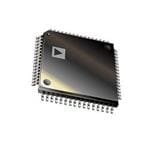
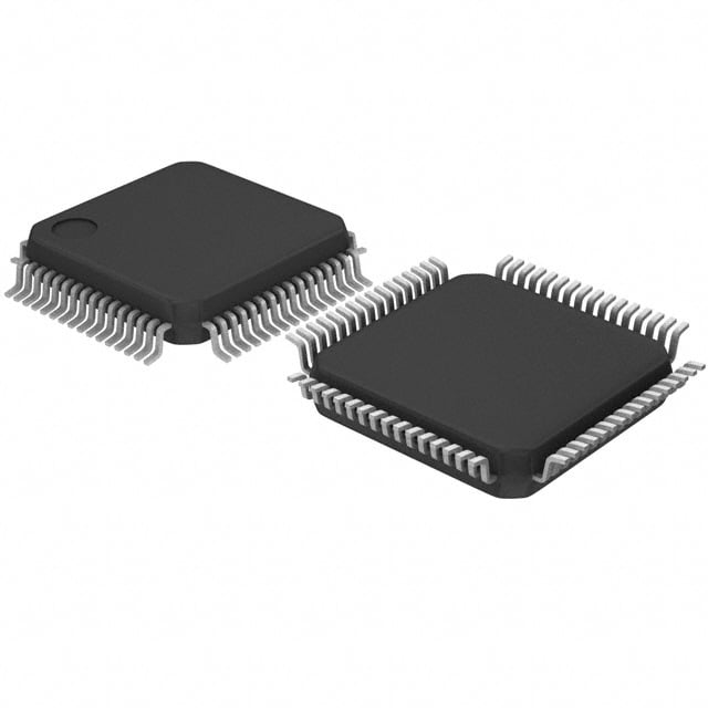
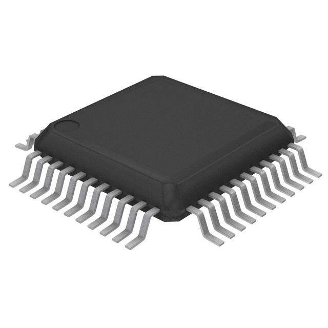
| 描述 | IC DAC 16BIT 40CH SERIAL 64-LQFP数模转换器- DAC 40-CH 16-bit Serial bipolar IC |
| 产品分类 | |
| 品牌 | Analog Devices Inc |
| 产品手册 | |
| 产品图片 |
|
| rohs | 符合RoHS无铅 / 符合限制有害物质指令(RoHS)规范要求 |
| 产品系列 | 数据转换器IC,数模转换器- DAC,Analog Devices AD5370BSTZ- |
| 数据手册 | |
| 产品型号 | AD5370BSTZ |
| 产品培训模块 | http://www.digikey.cn/PTM/IndividualPTM.page?site=cn&lang=zhs&ptm=19145http://www.digikey.cn/PTM/IndividualPTM.page?site=cn&lang=zhs&ptm=18614http://www.digikey.cn/PTM/IndividualPTM.page?site=cn&lang=zhs&ptm=26125http://www.digikey.cn/PTM/IndividualPTM.page?site=cn&lang=zhs&ptm=26140http://www.digikey.cn/PTM/IndividualPTM.page?site=cn&lang=zhs&ptm=26150http://www.digikey.cn/PTM/IndividualPTM.page?site=cn&lang=zhs&ptm=26147 |
| 产品种类 | 数模转换器- DAC |
| 位数 | 16 |
| 供应商器件封装 | 64-LQFP(10x10) |
| 分辨率 | 16 bit |
| 包装 | 托盘 |
| 商标 | Analog Devices |
| 安装类型 | 表面贴装 |
| 安装风格 | SMD/SMT |
| 封装 | Tray |
| 封装/外壳 | 64-LQFP |
| 封装/箱体 | LQFP-64 |
| 工作温度 | -40°C ~ 85°C |
| 工厂包装数量 | 160 |
| 建立时间 | 20µs |
| 接口类型 | Serial (Microwire, QSPI, SPI) |
| 数据接口 | SPI, DSP |
| 最大功率耗散 | 280 mW (Typ) |
| 最大工作温度 | + 85 C |
| 最小工作温度 | - 40 C |
| 标准包装 | 1 |
| 电压参考 | External |
| 电压源 | 双 ± |
| 电源电压-最大 | +/- 16.5 V |
| 电源电压-最小 | - 4.5 V, 9 V |
| 积分非线性 | +/- 4 LSB |
| 稳定时间 | 30 us |
| 系列 | AD5370 |
| 结构 | Resistor-String |
| 设计资源 | |
| 转换器数 | 40 |
| 转换器数量 | 40 |
| 输出数和类型 | 40 电压,单极40 电压,双极 |
| 输出类型 | Voltage Buffered |
| 采样率(每秒) | - |


- 商务部:美国ITC正式对集成电路等产品启动337调查
- 曝三星4nm工艺存在良率问题 高通将骁龙8 Gen1或转产台积电
- 太阳诱电将投资9.5亿元在常州建新厂生产MLCC 预计2023年完工
- 英特尔发布欧洲新工厂建设计划 深化IDM 2.0 战略
- 台积电先进制程称霸业界 有大客户加持明年业绩稳了
- 达到5530亿美元!SIA预计今年全球半导体销售额将创下新高
- 英特尔拟将自动驾驶子公司Mobileye上市 估值或超500亿美元
- 三星加码芯片和SET,合并消费电子和移动部门,撤换高东真等 CEO
- 三星电子宣布重大人事变动 还合并消费电子和移动部门
- 海关总署:前11个月进口集成电路产品价值2.52万亿元 增长14.8%


PDF Datasheet 数据手册内容提取
40-Channel,16-Bit, Serial Input, Voltage Output DAC AD5370 FEATURES 2.5 V to 5.5 V digital interface Digital reset (RESET) 40-channel DAC in a 64-lead LFCSP and a 64-lead LQFP Clear function to user-defined SIGGNDx Guaranteed monotonic to 16 bits Simultaneous update of DAC outputs Maximum output voltage span of 4 × V (20 V) REF Nominal output voltage span of −4 V to +8 V APPLICATIONS Multiple, independent output spans available Level setting in automatic test equipment (ATE) System calibration function allowing user-programmable Variable optical attenuators (VOA) offset and gain Optical switches Channel grouping and addressing features Industrial control systems Thermal shutdown function Instrumentation DSP/microcontroller-compatible serial interface SPI serial interface FUNCTIONAL BLOCK DIAGRAM DVCC VDD VSS AGND DGND LDAC VREF0 RCEOGNITSRTOELR 16 8 AR/BE GSIESLTEECRT 8 MTUOX2 16 REOGFISST0ER16 ODFAFCS E0T BUFFBEURFFEROUTPUT GBURFOFUEPR 0 1166 REGXXI11SABTER MUX 1 16 16 REGXXI22SABTER MUX 2 16 REDGAISCT 0ER16 DAC 0 POCWOEANRNT-DRDOOLWN VVVOOOUUUTTT012 REGISTER REGISTER 16 16 VOUT3 M REGISTER 16 16 VOUT4 C REGISTER VOUT5 VOUT6 OUTPUT BUFFER SYSNDCI INTSEERRFIAALCE 1166 REGXXI11SABTER MUX 1 16 16 REGXXI22SABTER MUX 2 16 REDGAISCT 7ER16 DAC 7 POCWOEANRNT-DRDOOLWN SVOIGUGTN7D0 REGISTER REGISTER SCLK 16 16 M REGISTER SDO 16 C REGISTER 16 VREF1 BUSY 16 16 BUFFER GROUP 1 OFS1 OFFSET RESET 8 AR/BE GSIESLTEECRT 8 MTUOX2 REGISTER DAC 1 BUFFER OUTPUT BUFFER CLR MSATCAHTINEE 1166 REGXXI11SABTER MUX 1 16 16 REGXXI22SABTER MUX 2 16 REDGAISCT 0ER16 DAC 0 POCWOEANRNT-DRDOOLWN VVVOOOUUUTTT8910 16 REGISTER 16 REGISTER VOUT11 16 M REGISTER 16 16 VOUT12 C REGISTER VOUT13 VOUT14 OUTPUT BUFFER 1166 REGXXI11SABTER MUX 1 16 16 REGXXI22SABTER MUX 2 16 REDGAISCT 7ER16 DAC 7 POCWOEANRNT-DRDOOLWN VSOIGUGTN1D51 REGISTER REGISTER 16 16 M REGISTER 16 16 C REGISTER AD5370 GROUP 2 TO GROUP 4 VOUT16 ARE THE SAME AS GROUP 1 TO VOUT39 SIGGND2 SIGGND3 SIGGND4 05813-001 Figure 1. Rev. 0 Information furnished by Analog Devices is believed to be accurate and reliable. However, no responsibility is assumed by Analog Devices for its use, nor for any infringements of patents or other One Technology Way, P.O. Box 9106, Norwood, MA 02062-9106, U.S.A. rights of third parties that may result from its use. Specifications subject to change without notice. No license is granted by implication or otherwise under any patent or patent rights of Analog Devices. Tel: 781.329.4700 www.analog.com Trademarks and registered trademarks are the property of their respective owners. Fax: 781.461.3113 ©2008 Analog Devices, Inc. All rights reserved.
AD5370 TABLE OF CONTENTS Features..............................................................................................1 Transfer Function.......................................................................17 Applications.......................................................................................1 Reference Selection....................................................................17 Functional Block Diagram..............................................................1 Calibration...................................................................................18 Revision History...............................................................................2 Additional Calibration...............................................................18 General Description.........................................................................3 Reset Function............................................................................19 Specifications.....................................................................................4 Clear Function............................................................................19 Performance Specifications.........................................................4 BUSY and LDAC Functions......................................................19 AC Characteristics........................................................................5 Power-Down Mode....................................................................19 Timing Characteristics................................................................6 Thermal Shutdown Function...................................................19 Timing Diagrams..........................................................................6 Toggle Mode................................................................................20 Absolute Maximum Ratings............................................................9 Serial Interface................................................................................21 ESD Caution..................................................................................9 SPI Write Mode..........................................................................21 Pin Configurations and Function Descriptions.........................10 SPI Readback Mode...................................................................21 Typical Performance Characteristics...........................................12 Register Update Rates................................................................21 Terminology....................................................................................14 Channel Addressing and Special Modes.................................21 Theory of Operation......................................................................15 Special Function Mode..............................................................23 DAC Architecture.......................................................................15 Power Supply Decoupling.........................................................25 Channel Groups..........................................................................15 Power Supply Sequencing.........................................................25 A/B Registers and Gain/Offset Adjustment............................16 Interfacing Examples.................................................................26 Load DAC....................................................................................16 Outline Dimensions.......................................................................27 Offset DAC Channels................................................................16 Ordering Guide..........................................................................27 Output Amplifier........................................................................17 REVISION HISTORY 4/08—Revision 0: Initial Version Rev. 0 | Page 2 of 28
AD5370 GENERAL DESCRIPTION The AD53701 contains forty 16-bit DACs in a single 64-lead The AD5370 has a high speed serial interface that is compatible LFCSP and a 64-lead LQFP. The device provides buffered with SPI, QSPI™, MICROWIRE™, and DSP interface standards voltage outputs with a span that is 4× the reference voltage. The and can handle clock speeds of up to 50 MHz. gain and offset of each DAC channel can be independently The DAC registers are updated on receipt of new data. All the trimmed to remove errors. For even greater flexibility, the device is outputs can be updated simultaneously by taking the LDAC divided into five groups of eight DACs. Three offset DAC channels input low. Each channel has a programmable gain and an offset allow the output range of blocks to be adjusted. Group 0 can be adjust register to allow removal of gain and offset errors. adjusted by Offset DAC 0, Group 1 can be adjusted by Offset Each DAC output is gained and buffered on chip with respect to DAC 1, and Group 2 to Group 4 can be adjusted by Offset DAC 2. an external SIGGNDx input. The DAC outputs can also be The AD5370 offers guaranteed operation over a wide supply switched to SIGGNDx via the CLR pin. range, with V from −16.5 V to −4.5 V and V from +9 V to SS DD +16.5 V. The output amplifier headroom requirement is 1.4 V operating with a load current of 1 mA. 1 Protected by U.S. Patent No. 5,969,657; other patents pending. Table 1. High Channel Count Bipolar DACs Model Resolution Nominal Output Span Output Channels Linearity Error (LSB) AD5360 16 bits 4 × V (20 V) 16 ±4 REF AD5361 14 bits 4 × V (20 V) 16 ±1 REF AD5362 16 bits 4 × V (20 V) 8 ±4 REF AD5363 14 bits 4 × V (20 V) 8 ±1 REF AD5370 16 bits 4 × V (12 V) 40 ±4 REF AD5371 14 bits 4 × V (12 V) 40 ±1 REF AD5372 16 bits 4 × V (12 V) 32 ±4 REF AD5373 14 bits 4 × V (12 V) 32 ±1 REF AD5378 14 bits ±8.75 V 32 ±3 AD5379 14 bits ±8.75 V 40 ±3 Rev. 0 | Page 3 of 28
AD5370 SPECIFICATIONS PERFORMANCE SPECIFICATIONS DV = 2.5 V to 5.5 V; V = 9 V to 16.5 V; V = −16.5 V to −8 V; V = 3 V; AGND = DGND = SIGGND = 0 V; C = open circuit; CC DD SS REF L R = open circuit; gain (M), offset (C), and DAC offset registers at default values; all specifications T to T , unless otherwise noted. L MIN MAX Table 2. Parameter Min Type Max Unit Test Conditions/Comments1 ACCURACY Resolution 16 Bits Integral Nonlinearity −4 +4 LSB Differential Nonlinearity −1 +1 LSB Guaranteed monotonic by design Zero-Scale Error −10 +10 mV Before calibration Full-Scale Error −10 +10 mV Before calibration Gain Error 0.1 % FSR Zero-Scale Error2 1 LSB After calibration Full-Scale Error2 1 LSB After calibration Span Error of Offset DAC −35 +35 mV See the Offset DAC Channels section for details VOUT Temperature Coefficient 5 ppm FSR/°C Includes linearity, offset, and gain drift (VOUT0 to VOUT39) DC Crosstalk2 120 μV Typically 20 μV; measured channel at midscale, full-scale change on any other channel REFERENCE INPUTS (VREF0, VREF1)2 VREF Input Current −10 +10 μA Per input, typically ±30 nA VREF Range 2 5 V ±2% for specified operation SIGGND INPUT (SIGGND0 to SIGGND4)2 DC Input Impedance 50 kΩ Typically 55 kΩ Input Range −0.5 +0.5 V SIGGND Gain 0.995 1.005 OUTPUT CHARACTERISTICS2 Output Voltage Range V + 1.4 V − 1.4 V I = 1 mA SS DD LOAD Nominal Output Voltage Range −4 +8 V Short-Circuit Current 15 mA VOUTx to DV , V , or V CC DD SS Load Current −1 +1 mA Capacitive Load 2200 pF DC Output Impedance 0.5 DIGITAL INPUTS Input High Voltage 1.7 V DV = 2.5 V to 3.6 V CC 2.0 V DV = 3.6 V to 5.5 V CC Input Low Voltage 0.8 V DV = 2.5 V to 5.5 V CC Input Current −1 +1 μA Excluding the CLR pin CLR High Impedance Leakage −20 +20 μA Current Input Capacitance2 10 pF DIGITAL OUTPUTS (SDO, BUSY) Output Low Voltage 0.5 V Sinking 200 μA Output High Voltage (SDO) DV − 0.5 V Sourcing 200 μA CC SDO High Impedance Leakage −5 +5 μA Current High Impedance Output 10 pF Capacitance2 Rev. 0 | Page 4 of 28
AD5370 Parameter Min Type Max Unit Test Conditions/Comments1 POWER REQUIREMENTS DV 2.5 5.5 V CC V 9 16.5 V DD V −16.5 −4.5 V SS Power Supply Sensitivity2 ∆Full Scale/∆V −75 dB DD ∆Full Scale/∆V −75 dB SS ∆Full Scale/∆DV −90 dB CC DI 2 mA DV = 5.5 V, V = DV , V = GND; normal CC CC IH CC IL operating conditions I 18 mA Outputs unloaded, DAC outputs = 0 V DD 20 mA Outputs unloaded, DAC outputs = full scale I −18 mA Outputs unloaded, DAC outputs = 0 V SS −20 mA Outputs unloaded, DAC outputs = full scale Power Dissipation Unloaded (P) 280 mW V = −8 V, V = +9.5 V, DV = 2.5 V SS DD CC Power-Down Mode Control register power-down bit set DI 5 μA CC I 35 μA DD I −35 μA SS Junction Temperature3 130 °C T = T + P × θ J A TOTAL JA 1 Temperature range for the AD5370 is −40°C to +85°C. Typical specifications are at 25°C. 2 Guaranteed by design and characterization, not production tested. 3 Where θJA represents the package thermal impedance. AC CHARACTERISTICS DV = 2.5 V; V = 15 V; V = −15 V; VREF0 = VREF1 = 3 V; AGND = DGND = SIGGND = 0 V; C = 200 pF; R = 10 kΩ; gain (M), CC DD SS L L offset (C), and DAC offset registers at default values; all specifications T to T , unless otherwise noted. MIN MAX Table 3. AC Characteristics1 Parameter Min Typ Max Unit Test Conditions/Comments DYNAMIC PERFORMANCE Output Voltage Settling Time 20 μs Settling to 1 LSB from a full-scale change 30 μs DAC latch contents alternately loaded with all 0s and all 1s Slew Rate 1 V/μs Digital-to-Analog Glitch Energy 5 nV-s Glitch Impulse Peak Amplitude 10 mV Channel-to-Channel Isolation 100 dB VREF0 = VREF1 = 2 V p-p, 1 kHz DAC-to-DAC Crosstalk 20 nV-s Digital Crosstalk 0.2 nV-s Digital Feedthrough 0.02 nV-s Effect of input bus activity on DAC output under test Output Noise Spectral Density @ 10 kHz 250 nV/√Hz VREF0 = VREF1 = 0 V 1 Guaranteed by design and characterization, not production tested. Rev. 0 | Page 5 of 28
AD5370 TIMING CHARACTERISTICS DV = 2.5 V to 5.5 V; V = 9 V to 16.5 V; V = −16.5 V to −4.5 V; V = 3 V; AGND = DGND = SIGGND = 0 V; C = 200 pF to GND; CC DD SS REF L R = open circuit; gain (M), offset (C), and DAC offset registers at default values; all specifications T to T , unless otherwise noted. L MIN MAX Table 4. SPI Interface Limit at T , T MIN MAX Parameter 1, 2, 3 Min Typ Max Unit Description t 20 ns SCLK cycle time 1 t 8 ns SCLK high time 2 t 8 ns SCLK low time 3 t 11 ns SYNC falling edge to SCLK falling edge setup time 4 t5 20 ns Minimum SYNC high time t 10 ns 24th SCLK falling edge to SYNC rising edge 6 t 5 ns Data setup time 7 t 5 ns Data hold time 8 t4 42 ns SYNC rising edge to BUSY falling edge 9 t 1.5 μs BUSY pulse width low (single-channel update); see Table 8 10 t 600 ns Single-channel update cycle time 11 t 20 ns SYNC rising edge to LDAC falling edge 12 t 10 ns LDAC pulse width low 13 t 3 μs BUSY rising edge to DAC output response time 14 t 0 ns BUSY rising edge to LDAC falling edge 15 t 3 μs LDAC falling edge to DAC output response time 16 t 20 30 μs DAC output settling time 17 t 140 ns CLR/RESET pulse activation time 18 t 30 ns RESET pulse width low 19 t 400 μs RESET time indicated by BUSY low 20 t 270 ns Minimum SYNC high time in readback mode 21 t 5 25 ns SCLK rising edge to SDO valid 22 t 80 ns RESET rising edge to BUSY falling edge 23 1 Guaranteed by design and characterization, not production tested. 2 All input signals are specified with tR = tF = 2 ns (10% to 90% of DVCC) and timed from a voltage level of 1.2 V. 3 See Figure 4 and Figure 5. 4 This is measured with the load circuit shown in Figure 2. 5 This is measured with the load circuit shown in Figure 3. TIMING DIAGRAMS DVCC 200µA IOL RL 2.2kΩ TO OUTPPUINT C50LpF VOL 05813-002 TO OUTPPUINT 50pCFL VOH (MIN) –2 VOL (MAX) 200µA IOH 05813-003 Figure 2. Load Circuit for BUSY Timing Diagram Figure 3. Load Circuit for SDO Timing Diagram Rev. 0 | Page 6 of 28
AD5370 t 1 SCLK 1 2 24 1 24 t3 t2 t11 t4 t6 SYNC t5 t 7 t 8 SDI DB23 DB0 t 9 t BUSY 10 t12 t13 LDAC1 t 17 t VOUTx1 14 t 15 t 13 LDAC2 t 17 VOUTx2 t16 CLR t 18 VOUTx t 19 RESET VOUTx t 18 t 20 BUSY t 23 21LLDDAACC AACCTTIIVVEE DAUFTREINRG B BUUSSYY.. 05813-004 Figure 4. SPI Write Timing Rev. 0 | Page 7 of 28
AD5370 t 22 SCLK 48 t 21 SYNC SDI DB23 DB0 DB23 DB0 INPUT WORD SPECIFIES NOP CONDITION REGISTER TO BE READ SDO DB0 DB23 DB0 LSB FROM PREVIOUS WRITE SELECTED REGISTER DATA CLOCKED OUT 05813-005 Figure 5. SPI Read Timing Rev. 0 | Page 8 of 28
AD5370 ABSOLUTE MAXIMUM RATINGS T = 25°C, unless otherwise noted. Transient currents of up to A Stresses above those listed under Absolute Maximum Ratings 60 mA do not cause SCR latch-up. may cause permanent damage to the device. This is a stress rating only; functional operation of the device at these or any Table 5. other conditions above those indicated in the operational Parameter Rating section of this specification is not implied. Exposure to absolute V to AGND −0.3 V to +17 V DD maximum rating conditions for extended periods may affect V to AGND −17 V to +0.3 V SS device reliability. DV to DGND −0.3 V to +7 V CC Digital Inputs to DGND −0.3 V to DV + 0.3 V CC Digital Outputs to DGND −0.3 V to DVCC + 0.3 V ESD CAUTION VREF0, VREF1 to AGND −0.3 V to +5.5 V VOUT0 through VOUT39 to AGND V − 0.3 V to V + 0.3 V SS DD SIGGND0 through SIGGND4 to AGND −1 V to +1 V AGND to DGND −0.3 V to +0.3 V Operating Temperature Range (TA) Industrial (B Version) −40°C to +85°C Storage −65°C to +150°C Operating Junction Temperature 130°C (T max) J θ Thermal Impedance JA 64-Lead LFCSP 25°C/W 64-Lead LQFP 45.5°C/W Reflow Soldering Peak Temperature 230°C Time at Peak Temperature 10 sec to 40 sec Rev. 0 | Page 9 of 28
AD5370 PIN CONFIGURATIONS AND FUNCTION DESCRIPTIONS CLRLDACVOUT26VOUT25VOUT24AGNDDGNDDVCCSDOSDISCLKSYNCDVCCDGNDVOUT7VOUT6 CLR LDAC VOUT26 VOUT25 VOUT24 AGND DGND DVCC SDO SDI SCLK SYNC DVCC DGND VOUT7 VOUT6 64636261605958575655545352515049 64 63 62 61 60 59 58 57 56 55 54 53 52 51 50 49 RESET 1 PIN 1 48 VOUT5 INDICATOR RESET 1 PIN 1 48VOUT5 BUSY 2 47 VOUT4 BUSY 2 INDICATOR 47VOUT4 VOUT27 3 46 SIGGND0 VOUT27 3 46SIGGND0 SIGGND3 4 45 VOUT3 SIGGND3 4 45VOUT3 VOUT28 5 44VOUT2 VOUT28 5 44 VOUT2 VOUT29 6 43VOUT1 VOUT29 6 43 VOUT1 VVOOUUTT3301 78 AD5370 4421VVOREUFT00 VOUT30 7 ATODP5 V3IE7W0 42 VOUT0 VOUT32 9 TOP VIEW 40VOUT23 VOUT31 8 (Not to Scale) 41 VREF0 VOUT3310 (Not to Scale) 39VOUT22 VOUT34 11 38VOUT21 VOUT32 9 40 VOUT23 VOUT3512 37VOUT20 VOUT33 10 39 VOUT22 SIGGND413 36VSS VOUT34 11 38 VOUT21 VOUT3614 35VDD VOUT3715 34SIGGND2 VOUT35 12 37 VOUT20 VDD16 33VOUT19 SIGGND4 13 36 VSS VOUT36 14 35 VDD VOUT37 15 34 SIGGND2 7890123456789012 V1SS1VREF11VOUT382VOUT392VOUT82VOUT92VOUT102VOUT112SIGGND1 2VOUT122VOUT132VOUT142VOUT153VOUT163VOUT173VOUT18 05813-007 VDD 16 V1SS7 VREF118 VOUT3819 VOUT3920 VOUT821 VOUT922 VOUT1023 2VOUT114 2SIGGND15 2VOUT126 2VOUT137 2VOUT148 2VOUT159 3VOUT160 3VOUT171 3VOUT182 33 VOUT1905813-025 Figure 6. 64-Lead LFCSP Pin Configuration Figure 7. 64-Lead LQFP Pin Configuration Table 6. Pin Function Descriptions Pin No. Mnemonic Description 1 RESET Digital Reset Input. 2 BUSY BUSY Input/Output (Active Low). BUSY is open-drain when an output. See the BUSY and LDAC Functions section for more information. 3, 5 to 12, 14, 15, 19 to VOUT0 to VOUT39 DAC Outputs. Buffered analog outputs for each of the 40 DAC channels. Each analog 24, 26 to 33, 37 to 40, 42 output is capable of driving an output load of 10 kΩ to ground. Typical output impedance to 45, 47 to 50, 60 to 62 of these amplifiers is 0.5 Ω. 46 SIGGND0 Reference Ground for DAC 0 to DAC 7. VOUT0 to VOUT7 are referenced to this voltage. 25 SIGGND1 Reference Ground for DAC 8 to DAC 15. VOUT8 to VOUT15 are referenced to this voltage. 34 SIGGND2 Reference Ground for DAC 16 to DAC 23. VOUT16 to VOUT23 are referenced to this voltage. 4 SIGGND3 Reference Ground for DAC 24 and DAC 31. VOUT24 to VOUT31 are referenced to this voltage. 13 SIGGND4 Reference Ground for DAC 32 to DAC 39. VOUT32 to VOUT39 are referenced to this voltage. 41 VREF0 Reference Input for DAC 0 to DAC 7. This reference voltage is referred to AGND. 18 VREF1 Reference Input for DAC 8 to DAC 39. This reference voltage is referred to AGND. Rev. 0 | Page 10 of 28
AD5370 Pin No. Mnemonic Description 16, 35 V Positive Analog Power Supply; +9 V to +16.5 V for specified performance. These pins DD should be decoupled with 0.1 μF ceramic capacitors and 10 μF capacitors. 17, 36 V Negative Analog Power Supply; −16.5 V to −8 V for specified performance. These pins SS should be decoupled with 0.1 μF ceramic capacitors and 10 μF capacitors. 51, 58 DGND Ground for All Digital Circuitry. Both DGND pins should be connected to the DGND plane. 52, 57 DV Logic Power Supply; 2.5 V to 5.5 V. These pins should be decoupled with 0.1 μF ceramic CC capacitors and 10 μF capacitors. 53 SYNC Active Low Input. This is the frame synchronization signal for the serial interface. See the Timing Characteristics section for more details. 54 SCLK Serial Clock Input. Data is clocked into the shift register on the falling edge of SCLK. This pin operates at clock speeds up to 50 MHz. See the Timing Characteristics section for more details. 55 SDI Serial Data Input. Data must be valid on the falling edge of SCLK. See the Timing Characteristics section for more details. 56 SDO Serial Data Output for SPI Interface. CMOS output. SDO can be used for readback. Data is clocked out on SDO on the rising edge of SCLK and is valid on the falling edge of SCLK. 59 AGND Ground for All Analog Circuitry. The AGND pin should be connected to the AGND plane. 63 LDAC Load DAC Logic Input (Active Low). 64 CLR Asynchronous Clear Input (Level Sensitive, Active Low). See the Clear Function section for more information. Exposed Paddle The lead-free chip scale package (LFCSP) has an exposed paddle on the underside. The paddle should be connected to V . SS Rev. 0 | Page 11 of 28
AD5370 TYPICAL PERFORMANCE CHARACTERISTICS 2 0 TA = 25°C VSS = –15V VDD = +15V VREF = +4.096V 1 V) B) E ( S D INL (L 0 MPLITU–0.01 A –1 –20 16384 DAC32C76O8DE 49152 65535 05813-009 –0.020 2 4TIME(µs) 6 8 10 05813-012 Figure 8.Typical INL Plot Figure 11. Analog Crosstalk Due to LDAC 0.0050 7 VDD = +15V TA = 25°C VSS = –15V VSS = –15V TA = 25°C VDD = +15V 6 VREF = +4.096V 0.0025 OF UNITS 54 TUDE (V) 0 R LI E P B 3 M M A U N 2 –0.0025 1 0 –0.6 –0.3 INL 0(LSB) 0.3 0.6 05813-010 –0.00500 1 2TIME (µs) 3 4 5 05813-013 Figure 9. Typical INL Distribution Figure 12. Digital Crosstalk 4 4 VDD = +15V VSS = –15V DVCC = +5V VREF = +3V 2 2 B) S B) OR (L 0 L (LS 0 R N R D E L N I –2 –2 –40 20 TEMPERA4T0URE (°C) 60 80 05813-011 –40 16384 DAC32C76O8DE 49152 65535 05813-014 Figure 10. Typical INL Error vs. Temperature Figure 13. Typical DNL Plot Rev. 0 | Page 12 of 28
AD5370 600 14 VDD = 15V VSS = 15V 500 12 TA = 25°C E (nV/ Hz) 400 OF UNITS 108 NOIS 300 BER 6 T M U U TP 200 N 4 U O 100 2 00 1 FR2EQUENCY(3Hz) 4 5 05813-015 0 13.00 13.25 ID1D3 .(5m0A) 13.75 14.00 05813-018 Figure 14. Noise Spectral Density Figure 17. Typical IDD Distribution 0.50 VVDSSD == –+1122VV 14 TDAV C=C 2 =5° 5CV VREF = +3V 12 0.45 S 10 DVCC = +5.5V NIT (mA)C 0.40 DVCC = +3.6V R OF U 8 DIC 0.35 MBE 6 DVCC = +2.5V NU 4 0.30 2 0.25–40 –20 0TEMPER20ATURE (°4C0) 60 80 05813-016 0 0.30 0.35 ICC0 .(4m0A) 0.45 0.50 05813-019 Figure 15.DICC vs. Temperature Figure 18. Typical DICC Distribution 14.0 IDD 13.5 A| ) m ( |S 13.0 /IDS ISS D I 12.5 VSS = –12V VDD = +12V VREF = +3V 12.0 –40 –20 0TEMPE2R0ATURE (4°C0) 60 80 05813-017 Figure 16. IDD/ISS vs. Temperature Rev. 0 | Page 13 of 28
AD5370 TERMINOLOGY Integral Nonlinearity (INL) significant at high load currents and reduces as the load currents Integral nonlinearity, or endpoint linearity, is a measure of the are reduced. With high impedance loads, the effect is virtually maximum deviation from a straight line passing through the immeasurable. Multiple V and V terminals are provided to DD SS endpoints of the DAC transfer function. It is measured after minimize dc crosstalk. adjusting for zero-scale error and full-scale error and is Output Voltage Settling Time expressed in least significant bits (LSB). The amount of time it takes for the output of a DAC to settle to Differential Nonlinearity (DNL) a specified level for a full-scale input change. Differential nonlinearity is the difference between the measured Digital-to-Analog Glitch Energy change and the ideal 1 LSB change between any two adjacent The amount of energy injected into the analog output at the codes. A specified differential nonlinearity of 1 LSB maximum major code transition. It is specified as the area of the glitch in ensures monotonicity. nV-s. It is measured by toggling the DAC register data between Zero-Scale Error 0x1FFF and 0x2000. Zero-scale error is the error in the DAC output voltage when all Channel-to-Channel Isolation 0s are loaded into the DAC register. Channel-to-channel isolation refers to the proportion of input Zero-scale error is a measure of the difference between VOUT signal from the reference input of one DAC that appears at the (actual) and VOUT (ideal), expressed in millivolts, when the output of another DAC operating from another reference. It is channel is at its minimum value. Zero-scale error is mainly due expressed in decibels and measured at midscale. to offsets in the output amplifier. DAC-to-DAC Crosstalk Full-Scale Error DAC-to-DAC crosstalk is the glitch impulse that appears at the Full-scale error is the error in DAC output voltage when all 1s output of one converter due to both the digital change and are loaded into the DAC register. Full-scale error is a measure subsequent analog output change at another converter. It is of the difference between VOUT (actual) and VOUT (ideal), specified in nV-s. expressed in millivolts, when the channel is at its maximum Digital Crosstalk value. It does not include zero-scale error. The glitch impulse transferred to the output of one converter Gain Error due to a change in the DAC register code of another converter is Gain error is the difference between full-scale error and zero- defined as the digital crosstalk and is specified in nV-s. scale error. It is expressed in millivolts. Digital Feedthrough Gain Error = Full-Scale Error − Zero-Scale Error When the device is not selected, high frequency logic activity on the digital inputs of the device can be capacitively coupled VOUT Temperature Coefficient both across and through the device to appear as noise on the This includes output error contributions from linearity, offset, VOUTx pins. It can also be coupled along the supply and and gain drift. ground lines. This noise is digital feedthrough. DC Output Impedance Output Noise Spectral Density DC output impedance is the effective output source resistance. Output noise spectral density is a measure of internally gener- It is dominated by package lead resistance. ated random noise. Random noise is characterized as a spectral DC Crosstalk density (voltage per √Hz). It is measured by loading all DACs The DAC outputs are buffered by op amps that share common to midscale and measuring noise at the output. It is measured V and V power supplies. If the dc load current changes in DD SS in nV/√Hz. one channel (due to an update), this can result in a further dc change in one or more channel outputs. This effect is more Rev. 0 | Page 14 of 28
AD5370 THEORY OF OPERATION DAC ARCHITECTURE CHANNEL GROUPS The AD5370 contains 40 DAC channels and 40 output amplifiers The 40 DAC channels of the AD5370 are arranged into five in a single package. The architecture of a single DAC channel groups of eight channels. The eight DACs of Group 0 derive consists of a 16-bit resistor-string DAC followed by an output their reference voltage from VREF0. Group 1 to Group 4 derive buffer amplifier. The resistor-string section is simply a string of their reference voltage from VREF1. Each group has its own resistors, of equal value, from VREF to AGND. This type of signal ground pin. architecture guarantees DAC monotonicity. The 16-bit binary digital code loaded to the DAC register determines at which node on the string the voltage is tapped off before being fed into the output amplifier. The output amplifier multiplies the DAC output voltage by 4. The nominal output span is 12 V with a 3 V reference and 20 V with a 5 V reference. Table 7. AD5370 Registers Word Register Length Default Name (Bits) Value Description X1A 16 0x1555 Input Data Register A. One for each DAC channel. X1B 16 0x1555 Input Data Register B. One for each DAC channel. M 16 0x3FFF Gain trim register. One for each DAC channel. C 16 0x2000 Offset trim register. One for each DAC channel. X2A 16 Not user Output Data Register A. One for each DAC channel. These registers store the final calibrated DAC accessible data after gain and offset trimming. They are not readable or directly writable. X2B 16 Not user Output Data Register B. One for each DAC channel. These registers store the final calibrated DAC accessible data after gain and offset trimming. They are not readable or directly writable. DAC Not user Data registers from which the DAC channels take their final input data. The DAC registers are accessible updated from the X2A or X2B register. They are not readable or directly writable. OFS0 14 0x1555 Offset DAC 0 data register. Sets the offset for Group 0. OFS1 14 0x1555 Offset DAC 1 data register. Sets the offset for Group 1 to Group 4. Control 3 0x00 Bit 2 = A/B. 0 = global selection of X1A input data registers. 1 = X1B registers. Bit 1 = enable temperature shutdown. 0 = disable temperature shutdown. 1 = enable. Bit 0 = soft power-down. 0 = soft power-up. 1 = soft power-down. A/B Select 0 8 0x00 Each bit in this register determines if a DAC channel in Group 0 takes its data from Register X2A or X2B. 0 = X2A. 1 = X2B. A/B Select 1 8 0x00 Each bit in this register determines if a DAC channel in Group 1 takes its data from Register X2A or X2B. 0 = X2A. 1 = X2B. A/B Select 2 8 0x00 Each bit in this register determines if a DAC channel in Group 2 takes its data from Register X2A or X2B. 0 = X2A. 1 = X2B. A/B Select 3 8 0x00 Each bit in this register determines if a DAC channel in Group 3 takes its data from Register X2A or X2B. 0 = X2A. 1 = X2B. A/B Select 4 8 0x00 Each bit in this register determines if a DAC channel in Group 4 takes its data from Register X2A or X2B. 0 = X2A. 1 = X2B. Rev. 0 | Page 15 of 28
AD5370 A/B REGISTERS AND GAIN/OFFSET ADJUSTMENT LOAD DAC Each DAC channel has seven data registers. The actual DAC All DAC channels in the AD5370 can be updated simultane- data-word can be written to either the X1A or X1B input register, ously by taking LDAC low when each DAC register is updated depending on the setting of the A/B bit in the Control register. from either its X2A or X2B register, depending on the setting of If the A/B bit is 0, data is written to the X1A register. If the A/B the A/B select registers. The DAC register is not readable or bit is 1, data is written to the X1B register. Note that this single directly writable by the user. bit is a global control and affects every DAC channel in the OFFSET DAC CHANNELS device. It is not possible to set up the device on a per-channel In addition to the gain and offset trim for each DAC channel, basis so that some writes are to X1A registers and some writes there are two 14-bit offset DAC channels, one for Group 0 and are to X1B registers. one for Group 1 to Group 4. These allow the output range of all X1A X2A DAC channels connected to them to be offset within a defined REGISTER REGISTER MUX MUX REGDIASCTER DAC range. Thus, subject to the limitations of headroom, it is possible to X1B X2B REGISTER REGISTER set the output range of Group 0 or Group 1 to Group 4 to be unipolar positive, unipolar negative, or bipolar, either symmetrical M REGISTER or asymmetrical about 0 V. The DAC channels in the AD5370 REGICSTER 05813-020 adreefa fualctt voarlyu etrs.i mThmise rde swuiltths itnh oe potfifmseutm D AofCfs ecth aanndn gealsin s epte arfto trhmeiarn ce Figure 19. Data Registers Associated with Each DAC Channel for the default output range and span. Each DAC channel also has a gain (M) register and an offset (C) When the output range is adjusted by changing the value of the register, which allow trimming out of the gain and offset errors offset DAC channel, an extra offset is introduced due to the of the entire signal chain. Data from the X1A register is operated on gain error of the offset DAC channel. The amount of offset is by a digital multiplier and an adder controlled by the contents of dependent on the magnitude of the reference and how much the M and C registers. The calibrated DAC data is then stored in the offset DAC channel deviates from its default value. This the X2A register. Similarly, data from the X1B register is operated offset is quoted in the Specifications section. on by the multiplier and adder and stored in the X2B register. The worst-case offset occurs when the offset DAC channel is at Although Figure 19 indicates a multiplier and an adder for each positive or negative full scale. This value can be added to the channel, there is only one multiplier and one adder in the device, offset present in the main DAC channel to give an indication of and they are shared among all channels. This has implications the overall offset for that channel. In most cases, the offset can be for the update speed when several channels are updated at once, removed by programming the channel’s C register with an as described in the Register Update Rates section. appropriate value. The extra offset caused by the offset DAC s only needs to be taken into account when an offset DAC Each time data is written to the X1A register, or to the M or C channel is changed from its default value. register with the A/B control bit set to 0, the X2A data is recal- culated and the X2A register is automatically updated. Similarly, Figure 20 shows the allowable code range that can be loaded to X2B is updated each time data is written to X1B or to M or C the offset DAC channel; this is dependent on the reference value with A/B set to 1. The X2A and X2B registers are not readable used. Thus, for a 5 V reference, the offset DAC channel should or directly writable by the user. not be programmed with a value greater than 8192 (0x2000). Data output from the X2A and X2B registers is routed to the 5 RESERVED final DAC register by a multiplexer. Whether each individual DAC takes its data from the X2A or X2B register is controlled 4 by an 8-bit A/B select register associated with each group of eight DACs. If a bit in this register is 0, the DAC takes its data 3 from the X2A register; if 1, the DAC takes its data from the X2B F)(V register (Bit 0 through Bit 7 control DAC0 to DAC7). RE V 2 Note that, because there are 40 bits in five registers, it is possible to set up, on a per-channel basis, whether each DAC takes its 1 data from the X2A or X2B register. A global command is also provided, which sets all bits in the A/B select registers to 0 or to 1. 00 4096 OFFSET8 1D9A2C CODE 12288 16383 05813-021 Figure 20. Offset DAC Code Range Rev. 0 | Page 16 of 28
AD5370 OUTPUT AMPLIFIER The input code is the value in the X1A or X1B register that is applied to DAC (X1A, X1B default code = 5461), as follows: The output amplifiers can swing to 1.4 V below the positive supply and 1.4 V above the negative supply, which limits how DAC_CODE=INPUT_CODE×(M+1)+C−215 much the output can be offset for a given reference voltage. For 216 example, it is not possible to have a unipolar output range of 20 V DAC output voltage is calculated as follows: because the maximum supply voltage is ±16.5 V. DAC_CODE − (4×OFFSET_CODE) VOUT=4×VREF× +V DAC S1 216 SIGGND CHANNEL VOUT R6 R5 S2 10kΩ where: 60kΩ CLR CLR DAC_CODE should be within the range of 0 to 65,535. 20Rk1Ω CLR S3 For 12 V span, VREF = 3.0 V. For 20 V span, VREF = 5.0 V. R4 R3 R2 SIGGND 60kΩ 20kΩ 20kΩ M = code in gain register − default code = 216 – 1. SIGGND C = code in offset register − default code = 215. OFFSET_CODE is the code loaded to the offset DAC. It is OFDFASCET 05813-022 multiplied by 4 in the transfer function because the offset DAC Figure 21. Output Amplifier and Offset DAC is a 14-bit device. On power-up, the default code loaded to the offset DAC is 5461 (0x1555). With a 3 V reference, this gives a Figure 21 shows details of a DAC output amplifier and its span of −4 V to +8 V. connections to its corresponding offset DAC. On power-up, S1 is open, disconnecting the amplifier from the output. S3 is REFERENCE SELECTION closed; thus, the output is pulled to the corresponding SIGGND The AD5370 has two reference input pins. The voltage applied (R1 and R2 are much greater than R6). S2 is also closed to to the reference pins determines the output voltage span on prevent the output amplifier being open-loop. If CLR is low at VOUT0 to VOUT39. VREF0 determines the voltage span for power-up, the output remains in this condition until CLR is VOUT0 to VOUT7 (Group 0) and VREF1 determines the taken high. The DAC registers can be programmed, and the voltage span for VOUT8 to VOUT39 (Group 2 to Group 4). outputs assume the programmed values when CLR is taken The reference voltage applied to each VREF pin can be high. Even if CLR is high at power-up, the output remains in the different, if required, allowing each group to have a different previously described condition until VDD > 6 V and VSS voltage span. The output voltage range and span can be adjusted < −4 V and the initialization sequence has finished. The outputs further by programming the offset and gain registers for each then go to their power-on default values. channel and by programming the offset DAC channels. If the offset and gain features are not used (that is, the M and C TRANSFER FUNCTION registers are left at their default values), the required reference OUTPUT levels can be calculated as follows: VOLTAGE FULL-SCALE 8V E+RROR VREF = (VOUTMAX − VOUTMIN)/4 ZERO-SCALE If the offset and gain features of the AD5370 are used, the ERROR ACTUAL required output range is slightly different. The chosen output TRANSFER FUNCTION range should take into account the system offset and gain errors that need to be trimmed out. Therefore, the chosen output IDEAL TRANSFER range should be larger than the actual required range. FUNCTION The required reference levels can be calculated as follows: 0 DAC CODE 16383 1. Identify the nominal output range on VOUT. 2. Identify the maximum offset span and the maximum gain required on the full output signal range. ZERO-SCALE –4V ERROR 3. Calculate the new maximum output range on VOUT, 05813-008 4. iCnhcoluodsein tgh et hnee wex rpeeqcutierded m VaOxiUmTuMmAX o afnfsde Vt aOnUd TgMaIiNn, keerreoprins.g Figure 22. DAC Transfer Function the VOUT limits centered on the nominal values. Note that V and V must provide sufficient headroom. The output voltage of a DAC in the AD5370 is dependent on the DD SS 5. Calculate the value of VREF as follows: value in the input register, the value of the M and C registers, and the value in the offset DAC. The transfer functions for the VREF = (VOUT − VOUT )/4 MAX MIN AD5370 are shown in the following section. Rev. 0 | Page 17 of 28
AD5370 Reference Selection Example Reducing Full-scale Error If Full-scale error can be reduced as follows: • Nominal Output Range = 12 V (−4 V to +8 V) 1. Measure the zero-scale error. • Zero-Scale Error = ±70 mV 2. Set the output to the highest possible value. • Gain Error = ±3% 3. Measure the actual output voltage and compare it with the • SIGGND = AGND = 0 V required value. Add this error to the zero-scale error. This is the span error, which includes the full-scale error. Then 4. Calculate the number of LSBs equivalent to the full-scale • Gain Error = ±3% error and subtract it from the default value of the M register. => Maximum Positive Gain Error = +3% Note that only positive full-scale error can be reduced. => Output Range Including Gain Error = 12 + 0.03(12) = 5. The M and C registers should not be programmed until 12.36 V both zero-scale and full-scale errors have been calculated. • Offset Error = ±70 mV AD5370 Calibration Example => Maximum Offset Error Span = 2(70 mV) = 0.14 V This example assumes that a −4 V to +8 V output is required. => Output Range Including Gain Error and Offset Error = The DAC output is set to −4 V but measured at −4.03 V. This 12.36 V + 0.14 V = 12.5 V gives a zero-scale error of −30 mV. • VREF Calculation Actual Output Range = 12.5 V, that is, −4.25 V to +8.25 V; 1. 1 LSB = 12 V/65,536 = 183.11 μV VREF = (8.25 V + 4.25 V)/4 = 3.125 V 2. 30 mV = 164 LSB If the equation yields an inconvenient reference level, the user The full-scale error can now be calculated. The output is set to can adopt one of the following approaches: +8 V and a value of +8.02 V is measured. The full-scale error is +20 mV – (–30 mV) = +50 mV. • Use a resistor divider to divide down a convenient, higher 50 mV = 273 LSBs reference level to the required level. • Select a convenient reference level above VREF, and modify The errors can now be removed. the gain and offset registers to downsize the reference digitally. 1. 164 LSB should be added to the default C register value, In this way, the user can use almost any convenient reference that is (32,768 + 164) = 32,932. level but may reduce the performance by overcompaction 2. 273 LSB should be subtracted from the default M register of the transfer function. value; that is, (65,535 − 273) = 65,262. • Use a combination of these two approaches. 3. 65,262 should be programmed to the M register and 32,932 CALIBRATION should be programmed to the C register. The user can perform a system calibration on the AD5370 to ADDITIONAL CALIBRATION reduce gain and offset errors to below 1 LSB. This is achieved The techniques described in the previous section are usually by calculating new values for the M and C registers and reprogram- enough to reduce the zero-scale and full-scale errors in most ming them. applications. However, there are limitations whereby the errors Reducing Zero-Scale Error may not be sufficiently removed. For example, the offset (C) register can only be used to reduce the offset caused by the Zero-scale error can be reduced as follows: negative zero-scale error. A positive offset cannot be reduced. 1. Set the output to the lowest possible value. Likewise, if the maximum voltage is below the ideal value, that 2. Measure the actual output voltage and compare it with the is, a negative full-scale error, the gain (M) register cannot be required value. This gives the zero-scale error. used to increase the gain to compensate for the error. 3. Calculate the number of LSBs equivalent to the error and These limitations can be overcome by increasing the reference add this from the default value of the C register. Note that value. With a 3 V reference, a 12 V span is achieved. The ideal only negative zero-scale error can be reduced. voltage range for the AD5370 is −4 V to +8 V. Using a 3.1 V reference increases the range to −4.133 V to +8.2667 V. Clearly, in this case, the offset and gain errors are insignificant, and the M and C registers can be used to raise the negative voltage to −4 V and then reduce the maximum voltage to +8 V to give the most accurate values possible. Rev. 0 | Page 18 of 28
AD5370 RESET FUNCTION high. Whenever the A/B select registers are written to, BUSY also goes low, for approximately 600 ns. The reset function is initiated by the RESET pin. On the rising edge of RESET, the AD5370 state machine initiates a reset The AD5370 has flexible addressing that allows writing of data sequence to reset the X, M, and C registers to their default to a single channel, all channels in a group, the same channel in values. This sequence typically takes 300 μs, and the user should Group 0 to Group 4 or the same channel in Group 1 to Group 4, not write to the part during this time. On power-up, it is recom- or all channels in the device. This means that 1, 4, 5, 8, or 40 mended that the user bring RESET high as soon as possible to DAC register values may need to be calculated and updated. properly initialize the registers. Because there is only one multiplier shared among 40 channels, this task must be done sequentially so that the length of the When the reset sequence is complete (and provided that CLR is BUSY pulse varies according to the number of channels being high), the DAC output is at a potential specified by the default updated. register settings, which are equivalent to SIGGNDx. The DAC outputs remain at SIGGNDx until the X, M, or C register is Table 8. BUSY Pulse Widths updated and LDAC is taken low. The AD5370 can be returned BUSY Pulse Width1 to the default state by pulsing RESET low for at least 30 ns. Note Action (μs max) that, because the reset function is triggered on the rising edge, Loading X1A, X1B, C, or M to 1 channel2 1.5 bringing RESET low has no effect on the operation of the AD5370. Loading X1A, X1B, C, or M to 4 channels 3.3 Loading X1A, X1B, C, or M to 5 channels 3.9 CLEAR FUNCTION Loading X1A, X1B, C, or M to 8 channels 5.7 CLR is an active low input that should be high for normal Loading X1A, X1B, C, or M to 40 channels 24.9 operation. The CLR pin has in internal 500 kΩ pull-down resistor. When CLR is low, the input to each of the DAC output 1 BUSY Pulse Width = ((Number of Channels + 1) × 600 ns) + 300 ns. 2 A single channel update is typically 1 μs. buffer stages, VOUT0 to VOUT39, is switched to the externally The AD5370 contains an extra feature whereby a DAC register set potential on the relevant SIGGND pin. While CLR is low, all is not updated unless its X2A or X2B register has been written LDAC pulses are ignored. When CLR is taken high again, the to since the last time LDAC was brought low. Normally, when DAC outputs remain cleared until LDAC is taken low. The contents LDAC is brought low, the DAC registers are filled with the of the input registers and DAC registers are not affected by taking contents of the X2A or X2B register, depending on the setting of CLR low. To prevent glitches from appearing on the outputs, CLR the A/B select registers. However, the AD5370 updates the DAC should be brought low by writing to the offset DAC whenever register only if the X2 data has changed, thereby removing the output span is adjusted. unnecessary digital crosstalk. BUSY AND LDAC FUNCTIONS POWER-DOWN MODE The value of an X2 (A or B) register is calculated each time the The AD5370 can be powered down by setting Bit 0 in the user writes new data to the corresponding X1, C, or M register. control register to 1. This turns off the DAC channels, thus During the calculation of X2, the BUSY output goes low. While reducing the current consumption. The DAC outputs are BUSY is low, the user can continue writing new data to the X1, connected to their respective SIGGND potentials. The power- M, or C register (see the Register Update Rates section for more down mode does not change the contents of the registers, and details), but no DAC output updates can take place. the DAC channels return to their previous voltage when the The BUSY pin is bidirectional and has a 50 kΩ internal pull-up power-down bit is cleared to 0. resistor. In cases where multiple AD5370 devices are used in THERMAL SHUTDOWN FUNCTION one system, the BUSY pins can be tied together. This is useful The AD5370 can be programmed to power down the DACs if when it is required that no DAC channel in any device be the temperature on the die exceeds 130°C. Setting Bit 1 in the updated until all other DAC channels are ready to be updated. control register to 1 (see the Special Function Mode section) When each device finishes updating the X2 (A or B) register, it enables this function. If the die temperature exceeds 130°C, the releases the BUSY pin. If another device has not finished AD5370 enters a temperature power-down mode, which is updating its X2 register, it holds BUSY low, thus delaying the equivalent to setting the power-down bit in the control register. effect of LDAC going low. To indicate that the AD5370 has entered temperature shutdown The DAC outputs are updated by taking the LDAC input low. If mode, Bit 4 of the control register is set to 1. The AD5370 remains LDAC goes low while BUSY is active, the LDAC event is stored in temperature shutdown mode, even if the die temperature falls, until Bit 1 in the control register is cleared to 0. and the DAC outputs update immediately after BUSY goes high. A user can also hold the LDAC input permanently low. In this case, the DAC outputs update immediately after BUSY goes Rev. 0 | Page 19 of 28
AD5370 TOGGLE MODE For the data generator example, the user need only set the high and low levels for each channel once by writing to the X1A and The AD5370 has two X2 registers per channel, X2A and X2B, X1B registers. The values of X2A and X2B are calculated and that can be used to switch the DAC output between two levels stored in their respective registers. The calculation delay with ease. This approach greatly reduces the overhead required therefore happens only during the setup phase, that is, when by a microprocessor that would otherwise have to write to each programming the initial values. To toggle a DAC output channel individually. When the user writes to the X1A, X2A, M, between the two levels, it is only required to write to the or C register, the calculation engine takes a certain amount of relevant A/B select register to set the MUX2 register bit. Further- time to calculate the appropriate X2A or X2B value. If the more, because there are eight MUX2 control bits per register, it application only requires that the DAC output switch between is possible to update eight channels with a single write. Table 15 two levels, as is the case with a data generator, any method that shows the bits that correspond to each DAC output. reduces the amount of calculation time necessary is advantageous. Rev. 0 | Page 20 of 28
AD5370 SERIAL INTERFACE The AD5370 contains a high speed SPI-compatible serial interface first two bits are the Special Function Code 00 to the device. The operating at clock frequencies up to 50 MHz (20 MHz for read remaining bits then determine which register is to be read back. operations). To minimize both the power consumption of the If a readback command is written to a special function register, device and on-chip digital noise, the interface powers up fully data from the selected register is clocked out of the SDO pin only when the device is being written to, that is, on the falling during the next SPI operation. The SDO pin is normally three- edge of SYNC. The serial interface is 2.5 V LVTTL-compatible stated but becomes driven as soon as a read command is issued. when operating from a 2.5 V to 3.6 V DVCC supply. It is con- The pin remains driven until the register data is clocked out. trolled by four pins: SYNC (frame synchronization input), SDI See Figure 5 for the read timing diagram. Note that, due to the (serial data input pin), SCLK (clocks data in and out of the device), timing requirements of t (25 ns), the maximum speed of the 5 and SDO (serial data output pin for data readback). SPI interface during a read operation should not exceed 20 MHz. SPI WRITE MODE REGISTER UPDATE RATES The AD5370 allows writing of data via the serial interface to The value of the X2A or X2B register is calculated each time the every register directly accessible to the serial interface, which is user writes new data to the corresponding X1, C, or M register. all registers except the X2A and X2B registers and the DAC The calculation is performed by a three-stage process. The first registers. The X2A and X2B registers are updated when the user two stages take approximately 600 ns each, and the third stage writes to the X1A, X1B, M, or C register, and the DAC registers takes approximately 300 ns. When the write to the X1, C, or M are updated by LDAC. register is complete, the calculation process begins. If the write operation involves the update of a single DAC channel, the user The serial word (see Table 10) is 24 bits long; 16 of these bits are is free to write to another register, provided that the write data bits, six bits are address bits, and two bits are mode bits that determine what is done with the data. operation does not finish until the first stage calculation is complete, that is, 600 ns after completion of the first write The serial interface works with both a continuous and a burst operation. If a group of channels is being updated by a single (gated) serial clock. Serial data applied to SDI is clocked into write operation, the first stage calculation is repeated for each the AD5370 by clock pulses applied to SCLK. The first falling channel, taking 600 ns per channel. In this case, the user should not edge of SYNC starts the write cycle. At least 24 falling clock edges complete the next write operation until this time has elapsed. must be applied to SCLK to clock in 24 bits of data before SYNC CHANNEL ADDRESSING AND SPECIAL MODES is taken high again. If SYNC is taken high before the 24th falling clock edge, the write operation is aborted. If the mode bits are not 00, the data-word for D13 to D0 is written to the device. Address Bit A5 to Address Bit A0 If a continuous clock is used, SYNC must be taken high before determine which channels are written to, whereas the mode bits the 25th falling clock edge. This inhibits the clock within the determine the register (X1A, X1B, C, or M) to which the data is AD5370. If more than 24 falling clock edges are applied before written, as shown in Table 9. If data is to be written to the X1A or SYNC is taken high again, the input data becomes corrupted. If X1B register, the setting of the A/B bit in the control register an externally gated clock of exactly 24 pulses is used, SYNC can determines the register to which the data is written (that is, be taken high any time after the 24th falling clock edge. 0 → X1A, 1 → X1B). The input register addressed is updated on the rising edge of Table 9. Mode Bits SYNC. For another serial transfer to take place, SYNC must be M1 M0 Action taken low again. 1 1 Writes to the DAC input data (X) register, SPI READBACK MODE depending on the control register A/B bit The AD5370 allows data readback via the serial interface from 1 0 Writes to the DAC offset (C) register every register directly accessible to the serial interface, which is 0 1 Writes to the DAC gain (M) register all registers except the X2A, X2B, and DAC registers. To read 0 0 Special function, used in combination back a register, it is first necessary to tell the AD5370 which with other bits of the data-word register to read. This is achieved by writing a word whose Table 10. Serial Word Bit Assignment I23 I22 I21 I20 I19 I18 I17 I16 I15 I14 I13 I12 I11 I10 I9 I8 I7 I6 I5 I4 I3 I2 I1 I0 M1 M0 A5 A4 A3 A2 A1 A0 D15 D14 D13 D12 D11 D10 D9 D8 D7 D6 D5 D4 D3 D2 D1 D0 Rev. 0 | Page 21 of 28
AD5370 Table 11 shows the groups and channels that are addressed for every combination of Address Bit A5 to Address Bit A0. Table 11. Group and Channel Addressing Address Bit A2 to Address Bit A5 to Address Bit A3 Address Bit A0 000 001 010 011 100 101 110 111 000 All groups, Group 0, Group 1, Group 2, Group 3, Group 4, Group 0, Group 1, all channels Channel 0 Channel 0 Channel 0 Channel 0 Channel 0 Group 1, Group 2, Group 2, Group 3, Group 3, Group 4; Group 4; Channel 0 Channel 0 001 Group 0, Group 0, Group 1, Group 2, Group 3, Group 4, Group 0, Group 1, all channels Channel 1 Channel 1 Channel 1 Channel 1 Channel 1 Group 1, Group 2, Group 2, Group 3, Group 3, Group 4; Group 4; Channel 1 Channel 1 010 Group 1, Group 0, Group 1, Group 2, Group 3, Group 4, Group 0, Group 1, all channels Channel 2 Channel 2 Channel 2 Channel 2 Channel 2 Group 1, Group 2, Group 2, Group 3, Group 3, Group 4; Group 4; Channel 2 Channel 2 011 Group 2, Group 0, Group 1, Group 2, Group 3, Group 4, Group 0, Group 1, all channels Channel 3 Channel 3 Channel 3 Channel 3 Channel 3 Group 1, Group 2, Group 2, Group 3, Group 3, Group 4; Group 4; Channel 3 Channel 3 100 Group 3, Group 0, Group 1, Group 2, Group 3, Group 4, Group 0, Group 1, all channels Channel 4 Channel 4 Channel 4 Channel 4 Channel 4 Group 1, Group 2, Group 2, Group 3, Group 3, Group 4; Group 4; Channel 4 Channel 4 101 Group 4, Group 0, Group 1, Group 2, Group 3, Group 4, Group 0, Group 1, all channels Channel 5 Channel 5 Channel 5 Channel 5 Channel 5 Group 1, Group 2, Group 2, Group 3, Group 3, Group 4; Group 4; Channel 5 Channel 5 110 Reserved Group 0, Group 1, Group 2, Group 3, Group 4, Group 0, Group 1, Channel 6 Channel 6 Channel 6 Channel 6 Channel 6 Group 1, Group 2, Group 2, Group 3, Group 3, Group 4; Group 4; Channel 6 Channel 6 111 Reserved Group 0, Group 1, Group 2, Group 3, Group 4, Group 0, Group 1, Channel 7 Channel 7 Channel 7 Channel 7 Channel 7 Group 1, Group 2, Group 2, Group 3, Group 3, Group 4; Group 4; Channel 7 Channel 7 Rev. 0 | Page 22 of 28
AD5370 SPECIAL FUNCTION MODE If the mode bits are 00, the special function mode is selected, as shown in Table 12. Bit I21 to Bit I16 of the serial data-word select the special function, and the remaining bits are data required for execution of the special function, for example, the channel address for data readback. The codes for the special functions are shown in Table 13. Table 14 shows the addresses for data readback. Table 12. Special Function Mode I23 I22 I21 I20 I19 I18 I17 I16 I15 I14 I13 I12 I11 I10 I9 I8 I7 I6 I5 I4 I3 I2 I1 I0 0 0 S5 S4 S3 S2 S1 S0 F15 F14 F13 F12 F11 F10 F9 F8 F7 F6 F5 F4 F3 F2 F1 F0 Table 13. Special Function Codes Special Function Code S5 S4 S3 S2 S1 S0 Data (F15 to F0) Action 0 0 0 0 0 0 0000 0000 0000 0000 NOP. 0 0 0 0 0 1 XXXX XXXX XXXX X [F2:F0] Write to the Control register. F4 = overtemperature indicator (read-only bit). This bit should be 0 when writing to the Control register. F3 = reserved. This bit should be 0 when writing to the Control register. F2 = 1: select register X1B for input. F2 = 0: select register X1A for input. F1 = 1: enable temperature shutdown. F1 = 0: disable temperature shutdown. F0 = 1: soft power-down. F0 = 0: soft power-up. 0 0 0 0 1 0 XX[F13:F0] Write data in F13:F0 to OFS0 register. 0 0 0 0 1 1 XX[F13:F0] Write data in F13:F0 to OFS1 register. 0 0 0 1 0 0 Reserved Reserved. 0 0 0 1 0 1 See Table 14 Select register for readback. 0 0 0 1 1 0 XXXX XXXX [F7:F0] Write data in F7:F0 to A/B Select Register 0. 0 0 0 1 1 1 XXXX XXXX [F7:F0] Write data in F7:F0 to A/B Select Register 1. 0 0 1 0 0 0 XXXX XXXX [F7:F0] Write data in F7:F0 to A/B Select Register 2. 0 0 1 0 0 1 XXXX XXXX [F7:F0] Write data in F7:F0 to A/B Select Register 3. 0 0 1 0 1 0 XXXX XXXX [F7:F0] Write data in F7:F0 to A/B Select Register 4. 0 0 1 0 1 1 XXXX XXXX [F7:F0] Block write A/B select registers. F7:F0 = 0, write all 0s (all channels use X2A register). F7:F0 = 1, write all 1s (all channels use X2B register). 0 1 1 1 0 0 Reserved Rev. 0 | Page 23 of 28
AD5370 Table 14. Address Codes for Data Readback1 F15 F14 F13 F12 F11 F10 F9 F8 F7 Register Read 0 0 0 Bit F12 to Bit F7 select the channel to be read back from; X1A register 0 0 1 Channel 0 = 001000 to Channel 39 = 101111 X1B register 0 1 0 C register 0 1 1 M register 1 0 0 0 0 0 0 0 1 Control register 1 0 0 0 0 0 0 1 0 OFS0 data register 1 0 0 0 0 0 0 1 1 OFS1 data register 1 0 0 0 0 0 1 0 0 Reserved 1 0 0 0 0 0 1 1 0 A/B Select Register 0 1 0 0 0 0 0 1 1 1 A/B Select Register 1 1 0 0 0 0 1 0 0 0 A/B Select Register 2 1 0 0 0 0 1 0 0 1 A/B Select Register 3 1 0 0 0 0 1 0 1 0 A/B Select Register 4 1 F6 to F0 are don’t cares for the data readback function. Table 15. DAC Channels Selected by A/B Select Registers A/B Select Bits1 Register F7 F6 F5 F4 F3 F2 F1 F0 0 VOUT7 VOUT6 VOUT5 VOUT4 VOUT3 VOUT2 VOUT1 VOUT0 1 VOUT15 VOUT14 VOUT13 VOUT12 VOUT11 VOUT10 VOUT9 VOUT8 2 VOUT23 VOUT22 VOUT21 VOUT20 VOUT19 VOUT18 VOUT17 VOUT16 3 VOUT31 VOUT30 VOUT29 VOUT28 VOUT27 VOUT26 VOUT25 VOUT24 4 VOUT39 VOUT38 VOUT37 VOUT36 VOUT35 VOUT34 VOUT33 VOUT32 1 If the bit is 0, Register A is selected. If the bit is 1, Register B is selected. Rev. 0 | Page 24 of 28
AD5370 POWER SUPPLY DECOUPLING Avoid crossover of digital and analog signals. Traces on opposite sides of the board should run at right angles to each other. This In any circuit where accuracy is important, careful consideration reduces the effects of feedthrough through the board. A microstrip of the power supply and ground return layout helps to ensure technique is by far the best approach, but it is not always possible the rated performance. The printed circuit board on which the with a double-sided board. In this technique, the component side AD5370 is mounted should be designed so that the analog and of the board is dedicated to ground plane, and signal traces are digital sections are separated and confined to certain areas of placed on the solder side. the board. If the AD5370 is in a system where multiple devices require an AGND-to-DGND connection, the connection should As is the case for all thin packages, care must be taken to avoid be made at one point only. The star ground point should be flexing the package and to avoid a point load on the surface of established as close as possible to the device. For supplies with this package during the assembly process. multiple pins (V , V , DV ), it is recommended to tie these SS DD CC POWER SUPPLY SEQUENCING pins together and to decouple each supply once. When the supplies are connected to the AD5370, it is important The AD5370 should have ample supply decoupling of 10 μF in that the AGND and DGND pins be connected to the relevant parallel with 0.1 μF on each supply located as close to the package ground plane before the positive or negative supplies are applied. as possible, ideally right up against the device. The 10 μF capacitors In most applications, this is not an issue because the ground pins are the tantalum bead type. The 0.1 μF capacitor should have for the power supplies are connected to the ground pins of the low effective series resistance (ESR) and low effective series AD5370 via ground planes. When the AD5370 is used in a hot inductance (ESI)—such as is typical of the common ceramic types swap card, care should be taken to ensure that the ground pins that provide a low impedance path to ground at high frequencies— are connected to the supply grounds before the positive or to handle transient currents due to internal logic switching. negative supply is connected. This is required to prevent currents Digital lines running under the device should be avoided from flowing in directions other than toward an analog or because they can couple noise onto the device. The analog digital ground. ground plane should be allowed to run under the AD5370 to avoid noise coupling. The power supply lines of the AD5370 should use as large a trace as possible to provide low impedance paths and reduce the effects of glitches on the power supply line. Fast-switching digital signals should be shielded with digital ground to avoid radiating noise to other parts of the board, and they should never be run near the reference inputs. It is essential to minimize noise on all VREF lines. Rev. 0 | Page 25 of 28
AD5370 INTERFACING EXAMPLES The Analog Devices ADSP-21065L is a floating point DSP with two serial ports (SPORTs). Figure 24 shows how one SPORT The SPI interface of the AD5370 is designed to allow the parts to be can be used to control the AD5370. In this example, the transmit easily connected to industry-standard DSPs and microcontrollers. frame synchronization (TFS) pin is connected to the receive Figure 23 shows how the AD5370 can be connected to the frame synchronization (RFS) pin. The transmit and receive Analog Devices, Inc., Blackfin® DSP. The Blackfin has an integrated clocks (TCLK and RCLK) are also connected together. The user SPI port that can be connected directly to the SPI pins of the can write to the AD5370 by writing to the transmit register. A read AD5370, as well as programmable input/output pins that can be operation can be accomplished by first writing to the AD5370 used to set or read the state of the digital input or output pins to tell the part that a read operation is required. A second write associated with the interface. operation with an NOP instruction causes the data to be read from the AD5370. The DSP receive interrupt can be used to AD5370 indicate when the read operation is complete. SPISELx SYNC SCK SCLK ADSP-21065L AD5370 MOSI SDI TFSx MISO SDO RFSx SYNC TCLKx PF10 RESET RCLKx SCLK ADSP-BF531 PF9 LDAC DTxA SDI PF8 CLR DRxA SDO PF7 BUSY 05813-023 FFLLAAGG01 RLDEASCET Figure 23. Interfacing to a Blackfin DSP FFLLAAGG23 CBLURSY 05813-024 Figure 24. Interfacing to an ADSP-21065L DSP Rev. 0 | Page 26 of 28
AD5370 OUTLINE DIMENSIONS 9.00 0.60 MAX BSC SQ 0.60 MAX PIN 1 INDICATOR 49 64 1 48 PIN 1 INDICATOR 0.50 7.25 TOP VIEW BS8C.7 5SQ BSC EXPOSED PAD 7.10 SQ (BOTTOM VIEW) 6.95 0.50 0.40 33 16 32 17 0.30 0.25 MIN 7.50 REF 1.00 12° MAX 0.80 MAX 0.65 TYP 0.85 0.05 MAX 0.80 0.02 NOM SEATING 0.30 PLANE 0.23 0.20 REF 0.18 COMPLIANT TO JEDEC STANDARDS MO-220-VMMD-4 051007-C Figure 25. 64-Lead Lead Frame Chip Scale Package [LFCSP_VQ] 9 mm × 9 mm Body, Very Thin Quad (CP-64-3) Dimensions shown in millimeters 12.20 0.75 12.00 SQ 0.60 1.60 11.80 0.45 MAX 64 49 1 48 PIN 1 10.20 TOP VIEW 10.00 SQ (PINS DOWN) 9.80 1.45 0.20 1.40 0.09 1.35 7° 3.5° 0.15 0° 16 33 0.05 SPLEAANTEING 0.08 17 32 COPLANARITY VIEW A 0.27 0.50 BSC 0.22 VIEW A LEAD PITCH 0.17 ROTATED 90° CCW COMPLIANTTO JEDEC STANDARDS MS-026-BCD 051706-A Figure 26. 64-Lead Low Profile Quad Flat Package [LQFP] (ST-64-2) Dimensions shown in millimeters ORDERING GUIDE Model Temperature Range Package Description Package Option AD5370BCPZ1 −40°C to +85°C 64-Lead Lead Frame Chip Scale Package (LFCSP_VQ) CP-64-3 AD5370BCPZ-REEL71 −40°C to +85°C 64-Lead Lead Frame Chip Scale Package (LFCSP_VQ) CP-64-3 AD5370BSTZ1 −40°C to +85°C 64-Lead Low Profile Quad Flat Package (LQFP) ST-64-2 AD5370BSTZ-REEL1 −40°C to +85°C 64-Lead Low Profile Quad Flat Package (LQFP) ST-64-2 1 Z = RoHS Compliant Part. Rev. 0 | Page 27 of 28
AD5370 NOTES © 2008 Analog Devices, Inc. All rights reserved. Trademarks and registered trademarks are the property of their respective owners. D05813-0-4/08(0) Rev. 0 | Page 28 of 28
Mouser Electronics Authorized Distributor Click to View Pricing, Inventory, Delivery & Lifecycle Information: A nalog Devices Inc.: AD5370BSTZ