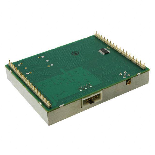
ICGOO在线商城 > 集成电路(IC) > 时钟/计时 - 专用 > AD9577BCPZ-R7

 Datasheet下载
- 型号: AD9577BCPZ-R7
- 制造商: Analog
- 库位|库存: xxxx|xxxx
- 要求:
| 数量阶梯 | 香港交货 | 国内含税 |
| +xxxx | $xxxx | ¥xxxx |
查看当月历史价格
查看今年历史价格
AD9577BCPZ-R7产品简介:
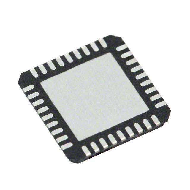
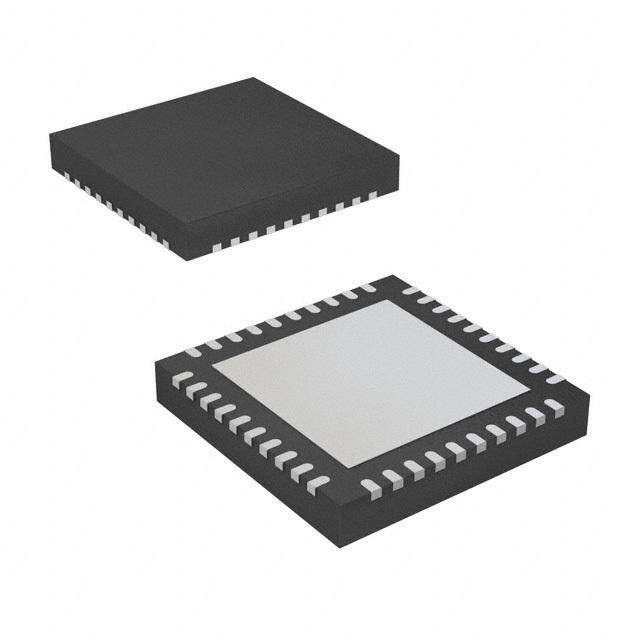
ICGOO电子元器件商城为您提供AD9577BCPZ-R7由Analog设计生产,在icgoo商城现货销售,并且可以通过原厂、代理商等渠道进行代购。 AD9577BCPZ-R7价格参考。AnalogAD9577BCPZ-R7封装/规格:时钟/计时 - 专用, Ethernet, PCI Express (PCIe), SONET/SDH Fanout Buffer (Distribution), Network Clock Generator IC 637.5MHz 1 Output 40-LFCSP-WQ (6x6)。您可以下载AD9577BCPZ-R7参考资料、Datasheet数据手册功能说明书,资料中有AD9577BCPZ-R7 详细功能的应用电路图电压和使用方法及教程。
AD9577BCPZ-R7是Analog Devices Inc.(亚德诺半导体)推出的一款专用时钟发生器,属于时钟/计时-专用类别。该器件主要面向高性能通信和网络设备,适用于对时钟精度、稳定性和低抖动要求极高的应用场景。

典型应用包括:无线基站(如4G LTE、5G基础设施)、光传输网络(OTN)、同步数字体系(SDH/SONET)设备以及测试与测量仪器。AD9577BCPZ-R7集成了锁相环(PLL)、多路输出缓冲器和可编程分频器,支持多种频率合成和时钟分配功能,能够为FPGA、ADC/DAC、高速收发器等关键器件提供精确的同步时钟信号。

其内置非易失性存储器可保存配置参数,上电后自动加载,简化系统设计并提升启动可靠性。同时,该芯片具备优秀的相位噪声性能和低抖动特性,确保高速数据链路的稳定运行。此外,它还支持频率裕量调节和冗余时钟输入切换,增强系统容错能力,适用于需要高可用性的电信和工业环境。

综上,AD9577BCPZ-R7广泛应用于对时序性能要求严苛的通信基础设施和高端电子系统中,是实现精准时钟管理的关键组件。
| 参数 | 数值 |
| 产品目录 | 集成电路 (IC) |
| 描述 | IC CLOCK GENERATOR 40LFCSP |
| 产品分类 | |
| 品牌 | Analog Devices Inc |
| 数据手册 | |
| 产品图片 |
|
| 产品型号 | AD9577BCPZ-R7 |
| PCN组件/产地 | |
| PLL | 是 |
| rohs | 无铅 / 符合限制有害物质指令(RoHS)规范要求 |
| 产品系列 | - |
| 主要用途 | 以太网,PCI Express(PCIe),SONET/SDH |
| 供应商器件封装 | 40-LFCSP-WQ(6x6) |
| 其它名称 | AD9577BCPZ-R7DKR |
| 包装 | Digi-Reel® |
| 安装类型 | 表面贴装 |
| 封装/外壳 | 40-WFQFN 裸露焊盘,CSP |
| 工作温度 | -40°C ~ 85°C |
| 差分-输入:输出 | 无/是 |
| 标准包装 | 1 |
| 比率-输入:输出 | 2:5 |
| 电压-电源 | 3 V ~ 3.6 V |
| 电路数 | 1 |
| 输入 | 时钟,晶体 |
| 输出 | LVCMOS,LVDS,LVPECL |
| 频率-最大值 | 637.5MHz |


- 商务部:美国ITC正式对集成电路等产品启动337调查
- 曝三星4nm工艺存在良率问题 高通将骁龙8 Gen1或转产台积电
- 太阳诱电将投资9.5亿元在常州建新厂生产MLCC 预计2023年完工
- 英特尔发布欧洲新工厂建设计划 深化IDM 2.0 战略
- 台积电先进制程称霸业界 有大客户加持明年业绩稳了
- 达到5530亿美元!SIA预计今年全球半导体销售额将创下新高
- 英特尔拟将自动驾驶子公司Mobileye上市 估值或超500亿美元
- 三星加码芯片和SET,合并消费电子和移动部门,撤换高东真等 CEO
- 三星电子宣布重大人事变动 还合并消费电子和移动部门
- 海关总署:前11个月进口集成电路产品价值2.52万亿元 增长14.8%


PDF Datasheet 数据手册内容提取
Clock Generator with Dual PLLs, Spread Spectrum, and Margining Data Sheet AD9577 FEATURES FUNCTIONAL BLOCK DIAGRAM Fully integrated dual PLL/VCO cores REFSEL 1 integer-N and 1 fractional-N PLL Continuous frequency coverage from 11.2 MHz to 200 MHz XXTT12 XOTSACL CMOS REFOUT Most frequencies from 200 MHz to 637.5 MHz available REFCLK PLL1 phase jitter (12 kHz to 20 MHz): 460 fs rms typical DIVIDE PLL2 phase jitter (12 kHz to 20 MHz) 1 OR 2 Integer-N mode: 470 fs rms typical PLL1 LDO IOnppFturiaot cnctraiyol srnteaaflle- oNrer m nrecoefde freree: n6qc6ue0e c nflsoc yrcm kd sfivr teiydqpeui-cebanylc -2y fPFD PFD/CP THIRDORDER LPF 22..15VT55COGGOHHzz DIVIDERS LOVRP 2E C× LC/LMVODSS I2C programmable output frequencies S R Up to 4 LVDS/LVPECL or up to 8 LVCMOS output clocks FEDEIVDIBDAECRK VIDE LOVRP 2E C× LC/LMVODSS 1 CMOS buffered reference clock output DI Spread spectrum: downspread [0, −0.5]% PLL2 LDO 2 pin-controlled frequency maps: margining PF S ISnptaecger astaevdin lgo,o 6p mfilmte ×rs 6 mm, 40-lead LFCSP package PFD/CP THIRDORDER L 22..15VT55COGGOHHzz DIVIDER OLVRP 2E C× LC/LMVODSS 1.02 W power dissipation (LVDS operation) S R 1.235 W power dissipation (LVPECL operation) FEDEIVDIBDAECRK VIDE LOVRP 2E C× LC/LMVODSS 3.3 V operation DI SCL I2C SDA CONTROL MARGIN ALoPwP jLitItCerA, TloIwO pNhSa se noise multioutput clock generator for MAXS_SBCWG SPREADS SDPMECTRUM, AD9577 09284-001 data communications applications including Ethernet, Figure 1. Fibre Channel, SONET, SDH, PCI-e, SATA, PTN, OTN, feedback divider, and two independently programmable output ADC/DAC, and digital video dividers. By connecting an external crystal or applying a reference Spread spectrum clocking clock to the REFCLK pin, frequencies of up to 637.5 MHz can be synchronized to the input reference. Each output divider and GENERAL DESCRIPTION feedback divider ratio is I2C programmed for the required output rates. The AD9577 provides a multioutput clock generator function, along with two on-chip phase-locked loop cores, PLL1 and PLL2, A second fractional-N PLL (PLL2) with a programmable modulus optimized for network clocking applications. The PLL designs allows VCO frequencies that are fractional multiples of the are based on the Analog Devices, Inc., proven portfolio of high reference frequency to be synthesized. Each output divider performance, low jitter frequency synthesizers to maximize and feedback divider ratio can be programmed for the required network performance. The PLLs have I2C programmable output output rates, up to 637.5 MHz. This fractional-N PLL can also frequencies and formats. The fractional-N PLL can support operate in integer-N mode for the lowest jitter. spread spectrum clocking for reduced EMI radiated peak power. Up to four differential output clock signals can be configured Both PLLs can support frequency margining. Other applications as either LVPECL or LVDS signaling formats. Alternatively, with demanding phase noise and jitter requirements can benefit the outputs can be configured for up to eight CMOS outputs. from this part. Combinations of these formats are supported. No external loop The first integer-N PLL section (PLL1) consists of a low noise phase filter components are required, thus conserving valuable design frequency detector (PFD), a precision charge pump (CP), a low time and board space. The AD9577 is available in a 40-lead, 6 mm × phase noise voltage controlled oscillator (VCO), a programmable 6 mm LFCSP package and can operate from a single 3.3 V supply. The operating temperature range is −40°C to +85°C. Rev. A Document Feedback Information furnished by Analog Devices is believed to be accurate and reliable. However, no responsibility is assumed by Analog Devices for its use, nor for any infringements of patents or other One Technology Way, P.O. Box 9106, Norwood, MA 02062-9106, U.S.A. rights of third parties that may result from its use. Specifications subject to change without notice. No license is granted by implication or otherwise under any patent or patent rights of Analog Devices. Tel: 781.329.4700 ©2011–2016 Analog Devices, Inc. All rights reserved. Trademarks and registered trademarks are the property of their respective owners. Technical Support www.analog.com
AD9577 Data Sheet TABLE OF CONTENTS Features .............................................................................................. 1 Example Application .................................................................. 28 Applications ....................................................................................... 1 Functional Description .................................................................. 29 General Description ......................................................................... 1 Reference Input and Reference Dividers ................................. 29 Functional Block Diagram .............................................................. 1 Output Channel Dividers .......................................................... 30 Revision History ............................................................................... 2 Outputs ........................................................................................ 30 Specifications ..................................................................................... 3 Reference Output Buffer ........................................................... 31 PLL1 Characteristics .................................................................... 3 PLL1 Integer-N PLL ................................................................... 31 PLL1 Clock Output Jitter ............................................................. 5 PLL1 Phase Frequency Detector (PFD) and Charge Pump . 32 PLL2 Fractional-N Mode Characteristics ................................. 6 PLL1 VCO ................................................................................... 32 PLL2 Integer-N Mode Characteristics ....................................... 7 PLL1 Feedback Divider ............................................................. 32 PLL2 Clock Output Jitter ............................................................. 9 Setting the Output Frequency of PLL1 .................................... 32 CMOS Reference Clock Output Jitter...................................... 11 PLL2 Integer/Fractional-N PLL ............................................... 32 Timing Characteristics .............................................................. 12 PLL2 Phase Frequency Detector (PFD) and Charge Pump . 33 Clock Outputs ............................................................................. 13 PLL2 Loop Bandwidth ............................................................... 33 Power ............................................................................................ 14 PLL2 VCO ................................................................................... 33 Crystal Oscillator ........................................................................ 15 PLL2 Feedback Divider ............................................................. 33 Reference Input ........................................................................... 15 PLL2 Σ-Δ Modulator ................................................................. 33 Control Pins ................................................................................ 15 Spur Mechanisms ....................................................................... 33 Absolute Maximum Ratings .......................................................... 16 Optimizing PLL Performance .................................................. 34 Thermal Characteristics ............................................................ 16 Setting the Output Frequency of PLL2 .................................... 34 ESD Caution ................................................................................ 16 Margining .................................................................................... 35 Pin Configuration and Function Descriptions ........................... 17 Spread Spectrum Clock Generation (SSCG) .......................... 35 Typical Performance Characteristics ........................................... 19 I2C Interface Timing and Internal Register Description ........... 38 REFOUT and PLL1 Phase Noise Performance ...................... 19 Default Frequency Map and Output Formats ........................ 40 PLL2 Phase Noise Performance ................................................ 20 I2C Interface Operation ............................................................. 40 Output Jitter ................................................................................ 21 Typical Application Circuits ..................................................... 42 Typical Output Signal ................................................................ 22 Power and Grounding Considerations and Power Supply Typical Spread Spectrum Performance Characteristics ........ 24 Rejection ...................................................................................... 43 Terminology .................................................................................... 25 Outline Dimensions ....................................................................... 44 Detailed Block Diagram ................................................................ 27 Ordering Guide .......................................................................... 44 REVISION HISTORY 8/2016—Rev. 0 to Rev. A Changes to Outputs Section .......................................................... 30 10/2011—Revision 0: Initial Version Rev. A | Page 2 of 44
Data Sheet AD9577 SPECIFICATIONS Typical (typ) is given for V = 3.3 V, T = 25°C, unless otherwise noted. Minimum (min) and maximum (max) values are given over full S A V (3.0 V to 3.6 V) and T (−40°C to +85°C) variation. AC coupling capacitors of 0.1 µF used where appropriate. A Fox Electronics S A FX532A 25 MHz crystal is used throughout, unless otherwise stated. PLL1 CHARACTERISTICS Table 1. Parameter Min Typ Max Unit Test Conditions/Comments1 NOISE CHARACTERISTICS Phase Noise (106.25 MHz LVPECL Output) Na = 102, Vx = 4, Dx = 6, f = 25 MHz PFD At 1 kHz −121 dBc/Hz At 10 kHz −127 dBc/Hz At 100 kHz −128 dBc/Hz At 1 MHz −150 dBc/Hz At 10 MHz −156 dBc/Hz At 30 MHz −158 dBc/Hz Phase Noise (156.25 MHz LVPECL Output) Na = 100, Vx = 4, Dx = 4, f = 25 MHz PFD At 1 kHz −117 dBc/Hz At 10 kHz −124 dBc/Hz At 100 kHz −124 dBc/Hz At 1 MHz −147 dBc/Hz At 10 MHz −156 dBc/Hz At 30 MHz −156 dBc/Hz Phase Noise (625 MHz LVPECL Output) Na = 100, Vx = 2, Dx = 2, f = 25 MHz PFD At 1 kHz −105 dBc/Hz At 10 kHz −112 dBc/Hz At 100 kHz −112 dBc/Hz At 1 MHz −135 dBc/Hz At 10 MHz −150 dBc/Hz At 30 MHz −150 dBc/Hz Phase Noise (106.25 MHz LVDS Output) Na = 102, Vx = 4, Dx = 6, f = 25 MHz PFD At 1 kHz −119 dBc/Hz At 10 kHz −127 dBc/Hz At 100 kHz −128 dBc/Hz At 1 MHz −148 dBc/Hz At 10 MHz −156 dBc/Hz At 30 MHz −156 dBc/Hz Phase Noise (156.25 MHz LVDS Output) Na = 100, Vx = 4, Dx = 4, f = 25 MHz PFD At 1 kHz −116 dBc/Hz At 10 kHz −124 dBc/Hz At 100 kHz −124 dBc/Hz At 1 MHz −145 dBc/Hz At 10 MHz −155 dBc/Hz At 30 MHz −155 dBc/Hz Phase Noise (625 MHz LVDS Output) Na = 100, Vx = 2, Dx = 2, f = 25 MHz PFD At 1 kHz −104 dBc/Hz At 10 kHz −111 dBc/Hz At 100 kHz −112 dBc/Hz At 1 MHz −134 dBc/Hz At 10 MHz −149 dBc/Hz At 30 MHz −149 dBc/Hz Rev. A | Page 3 of 44
AD9577 Data Sheet Parameter Min Typ Max Unit Test Conditions/Comments1 Phase Noise (106.25 MHz CMOS Output) Na = 102, Vx = 4, Dx = 6, f = 25 MHz PFD At 1 kHz −118 dBc/Hz At 10 kHz −127 dBc/Hz At 100 kHz −127 dBc/Hz At 1 MHz −149 dBc/Hz At 10 MHz −156 dBc/Hz At 30 MHz −157 dBc/Hz Phase Noise (156.25 MHz CMOS Output) Na = 100, Vx = 4, Dx = 4, f = 25 MHz PFD At 1 kHz −115 dBc/Hz At 10 kHz −124 dBc/Hz At 100 kHz −124 dBc/Hz At 1 MHz −146 dBc/Hz At 10 MHz −155 dBc/Hz At 30 MHz −155 dBc/Hz Phase Noise (155.52 MHz LVPECL Output) Na = 112, Vx = 2, Dx = 7, f = 19.44 MHz PFD At 1 kHz −117 dBc/Hz At 10 kHz −122 dBc/Hz At 100 kHz −123 dBc/Hz At 1 MHz −148 dBc/Hz At 10 MHz −156 dBc/Hz At 30 MHz −156 dBc/Hz Phase Noise (622.08 MHz LVPECL Output) Na = 128, Vx = 2, Dx = 2, f = 19.44 MHz PFD At 1 kHz −105 dBc/Hz At 10 kHz −110 dBc/Hz At 100 kHz −110 dBc/Hz At 1 MHz −136 dBc/Hz At 10 MHz −150 dBc/Hz At 30 MHz −150 dBc/Hz Phase Noise (155.52 MHz LVDS Output) Na = 112, Vx = 2, Dx = 7, f = 19.44 MHz PFD At 1 kHz −117 dBc/Hz At 10 kHz −122 dBc/Hz At 100 kHz −123 dBc/Hz At 1 MHz −146 dBc/Hz At 10 MHz −155 dBc/Hz At 30 MHz −155 dBc/Hz Phase Noise (622.08 MHz LVDS Output) Na = 128, Vx = 2, Dx = 2, f = 19.44 MHz PFD At 1 kHz −105 dBc/Hz At 10 kHz −110 dBc/Hz At 100 kHz −110 dBc/Hz At 1 MHz −134 dBc/Hz At 10 MHz −149 dBc/Hz At 30 MHz −150 dBc/Hz Phase Noise (155.52 MHz CMOS Output) Na = 112, Vx = 2, Dx = 7, f = 19.44 MHz PFD At 1 kHz −117 dBc/Hz At 10 kHz −122 dBc/Hz At 100 kHz −123 dBc/Hz At 1 MHz −147 dBc/Hz At 10 MHz −155 dBc/Hz At 30 MHz −155 dBc/Hz 1 x indicates either 0 or 1 for any given test condition. Rev. A | Page 4 of 44
Data Sheet AD9577 PLL1 CLOCK OUTPUT JITTER Table 2. Parameter1 Min Typ Max Unit Test Conditions/Comments2 LVPECL INTEGRATED RANDOM PHASE JITTER 25 MHz crystal used RMS Jitter (625 MHz Output) 460 750 fs rms 12 kHz to 20 MHz, Na = 100, Vx = 2, Dx = 2 430 650 fs rms 50 kHz to 80 MHz, Na = 100, Vx = 2, Dx = 2 RMS Jitter (156.25 MHz Output) 460 750 fs rms 12 kHz to 20 MHz, Na = 100, Vx = 4, Dx = 4 RMS Jitter (106.25 MHz Output) 460 750 fs rms 12 kHz to 20 MHz, Na = 102, Vx = 4, Dx = 6 LVDS INTEGRATED RANDOM PHASE JITTER 25 MHz crystal used RMS Jitter (625 MHz Output) 470 820 fs rms 12 kHz to 20 MHz, Na = 100, Vx = 2, Dx = 2 450 790 fs rms 50 kHz to 80 MHz, Na = 100, Vx = 2, Dx = 2 RMS Jitter (156.25 MHz Output) 470 790 fs rms 12 kHz to 20 MHz, Na = 100, Vx = 4, Dx = 4 RMS Jitter (106.25 MHz Output) 470 790 fs rms 12 kHz to 20 MHz, Na = 102, Vx = 4, Dx = 6 CMOS INTEGRATED RANDOM PHASE JITTER 25 MHz crystal used, 50 Ω load RMS Jitter (100 MHz Output) 470 920 f rms 12 kHz to 20 MHz, Na = 96, Vx = 4, Dx = 6 S RMS Jitter (33.3 MHz Output) 420 700 f rms 12 kHz to 5 MHz, Na = 88, Vx = 6, Dx = 11 S LVPECL INTEGRATED RANDOM PHASE JITTER 19.44 MHz crystal used RMS Jitter (622.08 MHz Output) 500 680 fs rms 12 kHz to 20 MHz, Na = 128, Vx = 2, Dx = 2 460 590 fs rms 50 kHz to 80 MHz, Na = 128, Vx = 2, Dx = 2 RMS Jitter (155.52 MHz Output) 480 680 fs rms 12 kHz to 20 MHz, Na = 112, Vx = 2, Dx = 7 LVDS INTEGRATED RANDOM PHASE JITTER 19.44 MHz crystal used RMS Jitter (622.08 MHz Output) 520 780 fs rms 12 kHz to 20 MHz, Na = 128, Vx = 2, Dx = 2 480 710 fs rms 50 kHz to 80 MHz, Na = 128, Vx = 2, Dx = 2 RMS Jitter (155.52 MHz Output) 480 750 fs rms 12 kHz to 20 MHz, Na = 112, Vx = 2, Dx = 7 CMOS INTEGRATED RANDOM PHASE JITTER 19.44 MHz crystal used, 50 Ω load RMS Jitter (155.52 MHz Output) 470 700 fs rms 12 kHz to 20 MHz, Na = 112, Vx = 2, Dx = 7 RMS Jitter (38.88 MHz Output) 440 650 fs rms 12 kHz to 5 MHz, Na = 112, Vx = 2, Dx = 28 LVPECL PERIOD AND CYCLE-TO-CYCLE JITTER (100 MHz OUTPUT) 25 MHz crystal used, Na = 96, Vx = 4, Dx = 6 Output Peak-to-Peak Period Jitter 13 ps p-p 10,000 cycles, average of 25 measurements Output RMS Period Jitter 2 ps rms 10,000 cycles, average of 25 measurements Output Peak-to-Peak, Cycle-to-Cycle Jitter 19 ps p-p 1,000 cycles, average of 25 measurements Output RMS Cycle-to-Cycle Jitter 3 ps rms 1,000 cycles, average of 25 measurements LVDS PERIOD AND CYCLE-TO-CYCLE JITTER (100 MHz OUTPUT) 25 MHz crystal used, Na = 96, Vx = 4, Dx = 6 Output Peak-to-Peak Period Jitter 17 ps p-p 10,000 cycles, average of 25 measurements Output RMS Period Jitter 2 ps rms 10,000 cycles, average of 25 measurements Output Peak-to-Peak, Cycle-to-Cycle Jitter 25 ps p-p 1,000 cycles, average of 25 measurements Output RMS Cycle-to-Cycle Jitter 4 ps rms 1,000 cycles, average of 25 measurements CMOS PERIOD AND CYCLE-TO-CYCLE JITTER (100 MHz OUTPUT) 25 MHz crystal used, 50 Ω load, Na = 96, Vx = 4, Dx = 6 Output Peak-to-Peak Period Jitter 25 ps p-p 10,000 cycles, average of 25 measurements Output RMS Period Jitter 3 ps rms 10,000 cycles, average of 25 measurements Output Peak-to-Peak Cycle-to-Cycle Jitter 36 ps p-p 1,000 cycles, average of 25 measurements Output RMS Cycle-to-Cycle Jitter 6 ps rms 1,000 cycles, average of 25 measurements 1 All period and cycle-to-cycle jitter measurements are made with a Tektronix DPO70604 oscilloscope. 2 x indicates either 0 or 1 for any given test condition. Rev. A | Page 5 of 44
AD9577 Data Sheet PLL2 FRACTIONAL-N MODE CHARACTERISTICS Table 3. Bleed = 1 Parameter Min Typ Max Unit Test Conditions/Comments1 NOISE CHARACTERISTICS 25 MHz crystal used Phase Noise (155.52 MHz LVPECL Output) Nb = 87, FRAC = 57, MOD = 625, Vx = 2, Dx = 7 At 1 kHz −107 dBc/Hz At 10 kHz −115 dBc/Hz At 100 kHz −122 dBc/Hz At 1 MHz −146 dBc/Hz At 10 MHz −153 dBc/Hz At 30 MHz −152 dBc/Hz Phase Noise (622.08 MHz LVPECL Output) Nb = 99, FRAC = 333, MOD = 625, Vx = 2, Dx = 2 At 1 kHz −95 dBc/Hz At 10 kHz −103 dBc/Hz At 100 kHz −109 dBc/Hz At 1 MHz −133 dBc/Hz At 10 MHz −148 dBc/Hz At 30 MHz −150 dBc/Hz Phase Noise (155.52 MHz LVDS Output) Nb = 87, FRAC = 57, MOD = 625, Vx = 2, Dx = 7 At 1 kHz −107 dBc/Hz At 10 kHz −114 dBc/Hz At 100 kHz −122 dBc/Hz At 1 MHz −145 dBc/Hz At 10 MHz −154 dBc/Hz At 30 MHz −154 dBc/Hz Phase Noise (622.08 MHz LVDS Output) Nb = 99, FRAC = 333, MOD = 625, Vx = 2, Dx = 2 At 1 kHz −95 dBc/Hz At 10 kHz −103 dBc/Hz At 100 kHz −109 dBc/Hz At 1 MHz −132 dBc/Hz At 10 MHz −147 dBc/Hz At 30 MHz −149 dBc/Hz Phase Noise (155.52 MHz CMOS Output) Nb = 87, FRAC = 57, MOD = 625, Vx = 2, Dx = 7 At 1 kHz −107 dBc/Hz At 10 kHz −114 dBc/Hz At 100 kHz −122 dBc/Hz At 1 MHz −146 dBc/Hz At 10 MHz −154 dBc/Hz At 30 MHz −154 dBc/Hz SPREAD SPECTRUM Modulation Range +0.1 −0.5 % Downspread, triangle modulation profile Modulation Frequency 31.25 kHz Programmable Peak Power Reduction 10 dB First harmonic of 100 MHz output, triangle modulation profile, spectrum analyzer resolution bandwidth = 20 kHz 1 x indicates either 2 or 3 for any given test condition. Rev. A | Page 6 of 44
Data Sheet AD9577 PLL2 INTEGER-N MODE CHARACTERISTICS Table 4. Bleed = 0 Parameter Min Typ Max Unit Test Conditions/Comments1 NOISE CHARACTERISTICS Phase Noise (106.25 MHz LVPECL Output) Nb = 102, Vx = 4, Dx = 6, f = 25 MHz PFD At 1 kHz −116 dBc/Hz At 10 kHz −123 dBc/Hz At 100 kHz −127 dBc/Hz At 1 MHz −148 dBc/Hz At 10 MHz −156 dBc/Hz At 30 MHz −158 dBc/Hz Phase Noise (156.25 MHz LVPECL Output) Nb = 100, Vx = 4, Dx = 4, f = 25 MHz PFD At 1 kHz −113 dBc/Hz At 10 kHz −120 dBc/Hz At 100 kHz −124 dBc/Hz At 1 MHz −146 dBc/Hz At 10 MHz −156 dBc/Hz At 30 MHz −156 dBc/Hz Phase Noise (625 MHz LVPECL Output) Nb = 100, Vx = 2, Dx = 2, f = 25 MHz PFD At 1 kHz −101 dBc/Hz At 10 kHz −108 dBc/Hz At 100 kHz −112 dBc/Hz At 1 MHz −134 dBc/Hz At 10 MHz −149 dBc/Hz At 30 MHz −150 dBc/Hz Phase Noise (106.25 MHz LVDS Output) Nb = 102, Vx = 4, Dx = 6, f = 25 MHz PFD At 1 kHz −117 dBc/Hz At 10 kHz −123 dBc/Hz At 100 kHz −127 dBc/Hz At 1 MHz −147 dBc/Hz At 10 MHz −156 dBc/Hz At 30 MHz −156 dBc/Hz Phase Noise (156.25 MHz LVDS Output) Nb = 100, Vx = 4, Dx = 4, f = 25 MHz PFD At 1 kHz −113 dBc/Hz At 10 kHz −120 dBc/Hz At 100 kHz −124 dBc/Hz At 1 MHz −145 dBc/Hz At 10 MHz −155 dBc/Hz At 30 MHz −155 dBc/Hz Phase Noise (625 MHz LVDS Output) Nb = 100, Vx = 2, Dx = 2, f = 25 MHz PFD At 1 kHz −101 dBc/Hz At 10 kHz −108 dBc/Hz At 100 kHz −112 dBc/Hz At 1 MHz −133 dBc/Hz At 10 MHz −148 dBc/Hz At 30 MHz −149 dBc/Hz Phase Noise (106.25 MHz CMOS Output) Nb = 102, Vx = 4, Dx = 6, f = 25 MHz PFD At 1 kHz −117 dBc/Hz At 10 kHz −123 dBc/Hz At 100 kHz −127 dBc/Hz At 1 MHz −147 dBc/Hz At 10 MHz −156 dBc/Hz At 30 MHz −157 dBc/Hz Rev. A | Page 7 of 44
AD9577 Data Sheet Parameter Min Typ Max Unit Test Conditions/Comments1 Phase Noise (156.25 MHz CMOS Output) Nb = 100, Vx = 4, Dx = 4, f = 25 MHz PFD At 1 kHz −113 dBc/Hz At 10 kHz −119 dBc/Hz At 100 kHz −123 dBc/Hz At 1 MHz −145 dBc/Hz At 10 MHz −154 dBc/Hz At 30 MHz −155 dBc/Hz Phase Noise (155.52 MHz LVPECL Output) Nb = 112, Vx = 2, Dx = 7, f = 19.44 MHz PFD At 1 kHz −112 dBc/Hz At 10 kHz −118 dBc/Hz At 100 kHz −126 dBc/Hz At 1 MHz −147 dBc/Hz At 10 MHz −155 dBc/Hz At 30 MHz −156 dBc/Hz Phase Noise (622.08 MHz LVPECL Output) Nb = 128, Vx = 2, Dx = 2, f = 19.44 MHz PFD At 1 kHz −100 dBc/Hz At 10 kHz −106 dBc/Hz At 100 kHz −112 dBc/Hz At 1 MHz −134 dBc/Hz At 10 MHz −149 dBc/Hz At 30 MHz −150 dBc/Hz Phase Noise (155.52 MHz LVDS Output) Nb = 112, Vx = 2, Dx = 7, f = 19.44 MHz PFD At 1 kHz −113 dBc/Hz At 10 kHz −118 dBc/Hz At 100 kHz −126 dBc/Hz At 1 MHz −145 dBc/Hz At 10 MHz −154 dBc/Hz At 30 MHz −155 dBc/Hz Phase Noise (622.08 MHz LVDS Output) Nb = 128, Vx = 2, Dx = 2, f = 19.44 MHz PFD At 1 kHz −101 dBc/Hz At 10 kHz −106 dBc/Hz At 100 kHz −112 dBc/Hz At 1 MHz −133 dBc/Hz At 10 MHz −148 dBc/Hz At 30 MHz −150 dBc/Hz Phase Noise (155.52 MHz CMOS Output) Nb = 112, Vx = 2, Dx = 7, f = 19.44 MHz PFD At 1 kHz −113 dBc/Hz At 10 kHz −118 dBc/Hz At 100 kHz −126 dBc/Hz At 1 MHz −146 dBc/Hz At 10 MHz −155 dBc/Hz At 30 MHz −155 dBc/Hz 1 x indicates either 2 or 3 for any given test condition. Rev. A | Page 8 of 44
Data Sheet AD9577 PLL2 CLOCK OUTPUT JITTER Table 5. Bleed = 0 for Integer-N Mode, Bleed = 1 for Fractional-N Mode Parameter1 Min Typ Max Unit Test Conditions/Comments2 LVPECL INTEGRATED RANDOM PHASE JITTER 25 MHz crystal used RMS Jitter (622.08 MHz Output) 660 1200 fs rms 12 kHz to 20 MHz, fractional-N operation, Nb = 99, FRAC = 333, MOD = 625, Vx = 2, Dx = 2 500 900 fs rms 50 kHz to 80 MHz, fractional-N operation, Nb = 99, FRAC = 333, MOD = 625, Vx = 2, Dx = 2 RMS Jitter (625 MHz Output) 470 800 fs rms 12 kHz to 20 MHz, integer-N operation, Nb = 100, Vx = 2, Dx = 2 380 650 fs rms 50 kHz to 80 MHz, integer-N operation, Nb = 100, Vx = 2, Dx = 2 RMS Jitter (155.52 MHz Output) 630 1100 fs rms 12 kHz to 20 MHz, fractional-N operation, Nb = 87, FRAC = 57, MOD = 625, Vx = 2, Dx = 7 RMS Jitter (156.25 MHz Output) 470 800 fs rms 12 kHz to 20 MHz, integer-N operation, Nb = 100, Vx = 4, Dx = 4 LVDS INTEGRATED RANDOM PHASE JITTER 25 MHz crystal used RMS Jitter (622.08 MHz Output) 660 1200 fs rms 12kHz to 20 MHz, fractional-N operation, Nb = 99, FRAC = 333, MOD = 625, Vx = 2, Dx = 2 510 900 fs rms 50 kHz to 80 MHz, fractional-N operation, Nb = 99, FRAC = 333, MOD = 625, Vx = 2, Dx = 2 RMS Jitter (625 MHz Output) 470 820 fs rms 12 kHz to 20 MHz, integer-N operation, Nb = 100, Vx = 2, Dx = 2 380 650 fs rms 50 kHz to 80 MHz, integer-N operation, Nb = 100, Vx = 2, Dx = 2 RMS Jitter (155.52 MHz Output) 620 1100 fs rms 12 kHz to 20 MHz, fractional-N operation, Nb = 87, FRAC = 57, MOD = 625, Vx = 2, Dx = 7 RMS Jitter (156.25 MHz Output) 480 800 fs rms 12 kHz to 20 MHz, integer-N operation, Nb = 100, Vx = 4, Dx = 4 CMOS INTEGRATED RANDOM PHASE JITTER 25 MHz crystal used, 50 Ω load RMS Jitter (155.52 MHz Output) 630 1100 fs rms 12 kHz to 20 MHz, fractional-N operation, Nb = 87, FRAC = 57, MOD = 625, Vx = 2, Dx = 7 RMS Jitter (100 MHz Output) 490 800 fs rms 12 kHz to 20 MHz, integer-N operation, Nb = 96, Vx = 4, Dx = 6 RMS Jitter (33.33 MHz Output) 450 700 fs rms 12 kHz to 5 MHz, integer-N operation, Nb = 88, Vx = 6, Dx = 11 LVPECL INTEGRATED RANDOM PHASE JITTER 19.44 MHz crystal used RMS Jitter (622.08 MHz Output) 510 800 fs rms 12 kHz to 20 MHz, integer-N operation, Nb = 128, Vx = 2, Dx = 2 380 650 fs rms 50 kHz to 80 MHz, integer-N operation, Nb = 128, Vx = 2, Dx = 2 RMS Jitter (155.52 MHz Output) 470 800 fs rms 12 kHz to 20 MHz, integer-N operation, Nb = 112, Vx = 2, Dx = 7 LVDS INTEGRATED RANDOM PHASE JITTER 19.44 MHz crystal used RMS Jitter (622.08 MHz Output) 530 900 fs rms 12 kHz to 20 MHz, integer-N operation, Nb = 128, Vx = 2, Dx = 2 390 700 fs rms 50 kHz to 80 MHz, integer-N operation, Nb = 128, Vx = 2, Dx = 2 RMS Jitter (155.52 MHz Output) 480 750 fs rms 12 kHz to 20 MHz, integer-N operation, Nb = 112, Vx = 2, Dx = 7 Rev. A | Page 9 of 44
AD9577 Data Sheet Parameter1 Min Typ Max Unit Test Conditions/Comments2 CMOS INTEGRATED RANDOM PHASE JITTER 19.44 MHz crystal used, 50 Ω load RMS Jitter (155.52 MHz Output) 470 700 fs rms 12 kHz to 20 MHz, integer-N operation, Nb = 112, Vx = 2, Dx = 7 RMS Jitter (38.88 MHz Output) 430 650 fs rms 12 kHz to 5 MHz, integer-N operation, Nb = 112, Vx = 2, Dx = 28 LVPECL PERIOD AND CYCLE-TO-CYCLE JITTER (100 MHz OUTPUT) 25 MHz crystal used, integer-N operation, Nb = 96, Vx = 4, Dx = 6 Output Peak-to-Peak Period Jitter 13 ps p-p 10,000 cycles, average of 25 measurements Output RMS Period Jitter 2 ps rms 10,000 cycles, average of 25 measurements Output Peak-to-Peak, Cycle-to-Cycle Jitter 19 ps p-p 1,000 cycles, average of 25 measurements Output RMS Cycle-to-Cycle Jitter 3 ps rms 1,000 cycles, average of 25 measurements LVDS PERIOD AND CYCLE-TO-CYCLE JITTER (100 MHz OUTPUT) 25 MHz crystal used, integer-N operation, Nb = 96, Vx = 4, Dx = 6 Output Peak-to-Peak Period Jitter 17 ps p-p 10,000 cycles, average of 25 measurements Output RMS Period Jitter 2 ps rms 10,000 cycles, average of 25 measurements Output Peak-to-Peak, Cycle-to-Cycle Jitter 26 ps p-p 1,000 cycles, average of 25 measurements Output RMS Cycle-to-Cycle Jitter 4 ps rms 1,000 cycles, average of 25 measurements CMOS PERIOD AND CYCLE-TO-CYCLE JITTER (100 MHz OUTPUT) 25 MHz crystal used, 50 Ω load, integer-N operation, Nb = 96, Vx = 4, Dx = 6 Output Peak-to-Peak Period Jitter 25 ps p-p 10,000 cycles, average of 25 measurements Output RMS Period Jitter 3 ps rms 10,000 cycles, average of 25 measurements Output Peak-to-Peak, Cycle-to-Cycle 36 ps p-p 1,000 cycles, average of 25 measurements Output RMS Cycle-to-Cycle Jitter 6 ps rms 1,000 cycles, average of 25 measurements LVPECL PERIOD AND CYCLE-TO-CYCLE JITTER (100 MHz OUTPUT) 25 MHz crystal used, SSCG on, Nb = 100, FRAC = 0, MOD = 1000, Vx = 5, Dx = 5, CkDiv = 7, NumSteps = 59, FracStep = −8, f = 100 MHz with −0.5% downspread OUT at 30.2 kHz Output Peak-to-Peak Period Jitter 60 ps p-p 10,000 cycles, average of 25 measurements Output RMS Period Jitter 15 ps rms 10,000 cycles, average of 25 measurements Output Peak-to-Peak, Cycle-to-Cycle Jitter 20 ps p-p 1,000 cycles, average of 25 measurements Output RMS Cycle-to-Cycle Jitter 3 ps rms 1,000 cycles, average of 25 measurements LVDS PERIOD AND CYCLE-TO-CYCLE JITTER (100 MHz OUTPUT) 25 MHz crystal used, SSCG on, Nb = 100, FRAC = 0, MOD = 1000, Vx = 5, Dx = 5, CkDiv = 7, NumSteps = 59, FracStep = −8, f = 100 MHz with −0.5% downspread OUT at 30.2 kHz Output Peak-to-Peak Period Jitter 63 ps p-p 10,000 cycles, average of 25 measurements Output RMS Period Jitter 15 ps rms 10,000 cycles, average of 25 measurements Output Peak-to-Peak, Cycle-to-Cycle Jitter 25 ps p-p 1,000 cycles, average of 25 measurements Output RMS Cycle-to-Cycle Jitter 4 ps rms 1,000 cycles, average of 25 measurements CMOS PERIOD AND CYCLE-TO-CYCLE JITTER (100 MHz OUTPUT) 25 MHz crystal used, SSCG on, 50 Ω load, Nb = 100, FRAC = 0, MOD = 1000, Vx = 5, Dx = 5, CkDiv = 7, NumSteps = 59, FracStep = −8, f = 100 MHz with OUT −0.5% downspread at 30.2 kHz Output Peak-to-Peak Period Jitter 70 ps p-p 10,000 cycles, average of 25 measurements Output RMS Period Jitter 15 ps rms 10,000 cycles, average of 25 measurements Output Peak-to-Peak, Cycle-to-Cycle Jitter 36 ps p-p 1,000 cycles, average of 25 measurements Output RMS Cycle-Cycle Jitter 6 ps rms 1,000 cycles, average of 25 measurements Rev. A | Page 10 of 44
Data Sheet AD9577 Parameter1 Min Typ Max Unit Test Conditions/Comments2 LVPECL PERIOD AND CYCLE-TO-CYCLE JITTER (100.12 MHz OUTPUT) 25 MHz crystal used, fractional-N operation, Nb = 100, FRAC = 15, MOD = 125, Vx = 5, Dx = 5 Output Peak-to-Peak Period Jitter 13 ps p-p 10,000 cycles, average of 25 measurements Output RMS Period Jitter 2 ps rms 10,000 cycles, average of 25 measurements Output Peak-to-Peak, Cycle-to-Cycle Jitter 20 ps p-p 1,000 cycles, average of 25 measurements Output RMS Cycle-to-Cycle Jitter 3 ps rms 1,000 cycles, average of 25 measurements LVDS PERIOD AND CYCLE-TO-CYCLE JITTER (100.12 MHz OUTPUT) 25 MHz crystal used, fractional-N operation, Nb = 100, FRAC = 15, MOD = 125, Vx = 5, Dx = 5 Output Peak-to-Peak Period Jitter 17 ps p-p 10,000 cycles, average of 25 measurements Output RMS Period Jitter 2 ps rms 10,000 cycles, average of 25 measurements Output Peak-to-Peak, Cycle-to-Cycle Jitter 26 ps p-p 1,000 cycles, average of 25 measurements Output RMS Cycle-to-Cycle Jitter 4 ps rms 1,000 cycles, average of 25 measurements CMOS PERIOD AND CYCLE-TO-CYCLE JITTER (100.12 MHz OUTPUT) 25 MHz crystal used, 50 Ω load, fractional-N operation, Nb = 100, FRAC = 15, MOD = 125, Vx = 5, Dx = 5 Output Peak-to-Peak Period Jitter 25 ps p-p 10,000 cycles, average of 25 measurements Output RMS Period Jitter 3 ps rms 10,000 cycles, average of 25 measurements Output Peak-to-Peak, Cycle-to-Cycle Jitter 36 ps p-p 1,000 cycles, average of 25 measurements Output RMS Cycle-to-Cycle Jitter 6 ps rms 1,000 cycles, average of 25 measurements 1 All period and cycle-to-cycle jitter measurements are made with a Tektronix DPO70604 oscilloscope. 2 x indicates either 2 or 3 for any given test condition. CMOS REFERENCE CLOCK OUTPUT JITTER Table 6. Parameter Min Typ Max Unit Test Conditions/Comments JITTER INTEGRATION BANDWIDTH Jitter measurement at 25 MHz is equipment limited 12 kHz to 5 MHz 680 1000 fs rms 25 MHz 200 kHz to 5 MHz 670 950 fs rms Rev. A | Page 11 of 44
AD9577 Data Sheet TIMING CHARACTERISTICS Table 7. Parameter Min Typ Max Unit Test Conditions/Comments LVPECL (see Figure 2) Termination = 200 Ω to 0 V, ac-coupled to 50 Ω oscilloscope; C = 5 pF LOAD Output Rise Time, t 170 225 300 ps 20% to 80%, measured differentially RP Output Fall Time, t 170 230 310 ps 80% to 20%, measured differentially FP Skew 20 ps Between the outputs of the same PLL at the same frequency. SyncCh01/SyncCh23 set to 1 LVDS (see Figure 3) Termination = 100 Ω differential; C = 5 pF LOAD Output Rise Time, t 180 250 340 ps 20% to 80%, measured differentially RL Output Fall Time, t 180 260 330 ps 80% to 20%, measured differentially FL Skew 20 ps Between the outputs of the same PLL at the same frequency; SyncCh01/SyncCh23 set to 1 CMOS (see Figure 4) Output Rise Time, t 250 680 950 ps Termination is high impedance active probe, RC total C = 5 pF, R = 20 kΩ, 20% to 80% LOAD LOAD Output Fall Time, t 350 700 1000 ps Termination is high impedance active probe, FC total C = 5 pF, R = 20 kΩ, 80% to 20% LOAD LOAD Skew 20 ps Between the outputs of the same PLL at the same frequency; SyncCh01/SyncCh23 set to 1 Timing Diagrams DIFFERENTIAL SINGLE-ENDED 80% 80% VOD 50% 20% 20% tRP LVPECL tFP 09284-002 tRC CMOS tFC 09284-004 Figure 2. LVPECL Timing, Differential Figure 4. CMOS Timing, Single-Ended, 5 pF Load DIFFERENTIAL 80% VOD 50% 20% LVDS tRL tFL 09284-003 Figure 3. LVDS Timing, Differential Rev. A | Page 12 of 44
Data Sheet AD9577 CLOCK OUTPUTS AC coupling capacitors of 0.1 µF used where appropriate. Table 8. Parameter Min Typ Max Unit Test Conditions/Comments LVPECL CLOCK OUTPUTS Output Frequency 637.5 MHz Load is 200 Ω to GND at output pins, then ac-coupled to 50 Ω terminated measurement equipment. Output Voltage Swing, V 610 740 950 mV Load is 200 Ω to GND at output pins, then OD ac-coupled to 50 Ω terminated measurement equipment. For differential amplitude, see Figure 2. Duty Cycle 45 55 % Load is 200 Ω to GND at output pins, then ac-coupled to 50 Ω terminated measurement equipment. Output High Voltage, V V − 1.24 V − 0.94 V − 0.83 V Load is 127 Ω/83 Ω potential divider across OH S S S supply dc-coupled into 1 MΩ terminated measurement equipment, outputs static. Output Low Voltage, V V − 2.07 V − 1.75 V − 1.62 V Load is 127 Ω/83 Ω potential divider across OL S S S supply dc-coupled into 1 MΩ terminated measurement equipment, outputs static. LVDS CLOCK OUTPUTS Output Frequency 637.5 MHz Load is ac-coupled to measurement equipment that provides 100 Ω differential input termination. Differential Output Voltage, V 250 350 475 mV Load is ac-coupled to measurement OD equipment that provides 100 Ω differential input termination. For differential amplitude, see Figure 3. Delta V 25 mV Load is ac-coupled to measurement OD equipment that provides 100 Ω differential input termination. Duty Cycle 45 55 % Load is ac-coupled to measurement equipment that provides 100 Ω differential input termination. Output Offset Voltage, V 1.125 1.25 1.375 V Load is dc-coupled to a 100 Ω differential OS resistor into 1 MΩ terminated measurement equipment, outputs static. Delta V 25 mV Load is dc-coupled to a 100 Ω differential OS resistor into 1 MΩ terminated measurement equipment, outputs static. Short-Circuit Current, I , I 13 24 mA Load is dc-coupled to a 100 Ω differential SA SB resistor into 1 MΩ terminated measurement equipment, output shorted to GND. CMOS CLOCK OUTPUTS Output Frequency 200 MHz Output High Voltage, V V − 0.15 V Sourcing 1.0 mA current, outputs static. OH S Output Low Voltage, V 0.1 V Sinking 1.0 mA current, outputs static. OL Duty Cycle 45 55 % Termination is high impedance active probe; total C = 5 pF, R = 20 kΩ. LOAD LOAD Rev. A | Page 13 of 44
AD9577 Data Sheet POWER Table 9. Parameter Min Typ Max Unit Test Conditions/Comments POWER SUPPLY 3.0 3.3 3.6 V LVPECL POWER DISSIPATION 1235 1490 mW Typical part configuration, both PLLs enabled for integer-N operation, f = 156.25 MHz, f = 125 MHz, f = 100 MHz, f = 33.33 MHz, OUT0 OUT1 OUT2 OUT3 Na = 100, V0 = 4, D0 = 4, V1 = 4, D1 = 5, Nb = 96, V2 = 4, D2 = 6, V3 = 4, D3 = 18, 25 MHz crystal used, load is 200 Ω to GND at output pins, then ac-coupled to 50 Ω terminated measurement equipment 1270 1530 mW Worst-case part configuration, PLL2 in fractional-N mode, with SSCG enabled, f = 379.16 MHz, f = 379.16 MHz, f = 359.33 MHz, OUT0 OUT1 OUT2 f = 359.33 MHz, Na = 91, V0 = 3, D0 = 2, V1 = 3, D1 = 2, Nb = 86, OUT3 V2 = 3, D2 = 2, V3 = 3, D3 = 2, FRAC = 300, MOD = 1250, CkDiv = 5, NumSteps = 77, FracStep = −7, −0.5% downspread at 32 kHz, 25 MHz crystal used, load is 200 Ω to GND at output pins, then ac-coupled to 50 Ω terminated measurement equipment LVDS POWER DISSIPATION 1020 1200 mW Typical part configuration, both PLLs enabled for integer-N operation, f = 156.25 MHz, f = 125 MHz, f = 100 MHz, f = 33.33 MHz, OUT0 OUT1 OUT2 OUT3 Na = 100, V0 = 4, D0 = 4, V1 = 4, D1 = 5, Nb = 96, V2 = 4, D2 = 6, V3 = 4, D3 = 18, 25 MHz crystal used, load ac-coupled to measurement equipment that provides 100 Ω differential input termination 1085 1290 mW Worst-case part configuration, PLL2 in fractional-N mode, with SSCG enabled, f = 379.16 MHz, f = 379.16 MHz, f = 359.33 MHz, OUT0 OUT1 OUT2 f = 359.33 MHz, Na = 91, V0 = 3, D0 = 2, V1 = 3, D1 = 2, Nb = 86, OUT3 V2 = 3, D2 = 2, V3 = 3, D3 = 2, FRAC = 300, MOD = 1250, CkDiv = 5, NumSteps = 77, FracStep = −7, −0.5% downspread at 32 kHz, 25 MHz crystal used, load ac-coupled to measurement equipment that provides 100 Ω differential input termination CMOS POWER DISSIPATION 1065 1380 mW Typical part configuration, both PLLs enabled for integer-N operation, f = 156.25 MHz, f = 125 MHz, f = 100 MHz, f = 33.33 MHz, OUT0 OUT1 OUT2 OUT3 Na = 100, V0 = 4, D0 = 4, V1 = 4, D1 = 5, Nb = 96, V2 = 4, D2 = 6, V3 = 4, D3 = 18, 25 MHz crystal used, eight single-ended outputs active, C = 5 pF LOAD 1190 1510 mW Worst-case part configuration, PLL2 in fractional-N mode, with SSCG enabled, f = 189.58 MHz, f = 189.58 MHz, f = 179.66 MHz, OUT0 OUT1 OUT2 f = 179.66 MHz, Na = 91, V0 = 3, D0 = 4, V1 = 3, D1 = 4, Nb = 86, OUT3 V2 = 3, D2 = 4, V3 = 3, D3 = 4, FRAC = 300, MOD = 1250, CkDiv = 5, NumSteps = 77, FracStep = −7, −0.5% downspread at 32 kHz, 25 MHz crystal used, eight single-ended outputs active, C = 5 pF LOAD POWER CHANGES Reduction in power due to turning off a channel of one VCO divider, one output divider, and one output buffer; data for Channel 1, with typical part configuration, both PLLs enabled for integer-N operation, f = 156.25 MHz, f = 125 MHz, f = 100 MHz, f = 33.33 MHz, OUT0 OUT1 OUT2 OUT3 Na = 100, V0 = 4, D0 = 4, V1 = 4, D1 = 5, Nb = 96, V2 = 4, D2 = 6, V3 = 4, D3 = 18, 25 MHz crystal used Power-Down 1 LVPECL Channel 160 205 mW Load 200 Ω to GND at output pins, and ac-coupled to 50 Ω terminated measurement equipment Power-Down 1 LVDS Channel 105 155 mW Load ac-coupled to measurement equipment that provides 100 Ω differential input termination Power-Down 1 CMOS Channel 130 170 mW Eight single-ended outputs active, C = 5 pF LOAD Rev. A | Page 14 of 44
Data Sheet AD9577 CRYSTAL OSCILLATOR Table 10. Parameter Min Typ Max Unit Test Conditions/Comments CRYSTAL SPECIFICATION Fundamental mode Frequency 19.44 25 27 MHz Reference divider, R = 1, only ESR 50 Ω Load Capacitance 14 pF Phase Noise −135 dBc/Hz 1 kHz offset Stability −50 +50 ppm REFERENCE INPUT Table 11. Parameter Min Typ Max Unit Test Conditions/Comments CLOCK INPUT (REFCLK) Input Frequency 19.44 25 27 MHz Reference divider, R = 1 38.88 50 54 MHz Reference divider, R = 2 Input High Voltage 2.0 V Input Low Voltage 0.8 V Input Current −1.0 +1.0 µA Input Capacitance 2 pF CONTROL PINS Table 12. Parameter Min Typ Max Unit Test Conditions/Comments INPUT CHARACTERISTICS SSCG, MAX_BW, and MARGIN SSCG, MAX_BW, and MARGIN have a 30 kΩ internal pull-down resistor Logic 1 Voltage 2.0 V Logic 0 Voltage 0.8 V Logic 1 Current 240 µA Logic 0 Current 40 µA REFSEL REFSEL has a 30 kΩ internal pull-up resistor Logic 1 Voltage 2.0 V Logic 0 Voltage 0.8 V Logic 1 Current 70 µA Logic 0 Current 240 µA I2C DC CHARACTERISTICS LVCMOS; the SCL and SDA pins only, see Figure 48 Input Voltage High 0.7 Vcc V Input Voltage Low 0.3 Vcc V Input Current −10 +10 µA V = 0.1 V or V = 0.9 V IN CC IN CC Output Low Voltage 0.4 V V with a load current of I = 3.0 mA OL OL I2C TIMING CHARACTERISTICS LVCMOS; the SCL and SDA pins only, see Figure 48 SCL Clock Frequency 400 kHz SCL Pulse Width High High, t 600 ns HIGH Low, t 1300 ns LOW Start Condition Hold Time, t 600 ns HD; STA Setup Time, t 600 ns SU; STA Data Setup Time, t 100 ns SU; DAT Hold Time, t 300 ns HD; DAT Stop Condition Setup Time, t 600 ns SU; STO Bus Free Time Between a Stop and a Start, t 1300 ns BUF Rev. A | Page 15 of 44
AD9577 Data Sheet ABSOLUTE MAXIMUM RATINGS THERMAL CHARACTERISTICS Table 13. Thermal impedance measurements were taken on a 4-layer Parameter Rating board in still air in accordance with EIA/JESD51-7. V to GND −0.3 V to +3.6 V S REFCLK to GND −0.3 V to V + 0.3 V S Table 14. Thermal Resistance LDO to GND −0.3V to V + 0.3 V S Package Type θ Unit JA XT1, XT2 to GND −0.3 V to V + 0.3 V S 40-Lead LFCSP 27.5 °C/W SSCG, MAX_BW, MARGIN, SCL, SDA, −0.3 V to V + 0.3 V S REFSEL to GND REFOUT, OUTxP, OUTxN to GND −0.3 V to VS + 0.3 V ESD CAUTION Junction Temperature1 150°C Storage Temperature −65°C to+150°C Lead Temperature (10 sec) 300°C 1 See the Thermal Characteristics section for θJA. Stresses at or above those listed under Absolute Maximum Ratings may cause permanent damage to the product. This is a stress rating only; functional operation of the product at these or any other conditions above those indicated in the operational section of this specification is not implied. Operation beyond the maximum operating conditions for extended periods may affect product reliability. Rev. A | Page 16 of 44
Data Sheet AD9577 PIN CONFIGURATION AND FUNCTION DESCRIPTIONS W A B_XAMA2TSTAVSVLCSDNGDNGP0TUON0TUO0BOSVADS 0987654321 4333333333 VSCA 1 PIN 1 30 VSOB1A VSI2C 2 INDICATOR 29 OUT1P REFOUT 3 28 OUT1N VSREFOUT 4 AD9577 27 VSFA VSX 5 26 SSCG REFCLK 6 TOP VIEW 25 VSM (Not to Scale) XT2 7 24 VSFB XT1 8 23 OUT3P REFSEL 9 22 OUT3N VSCB 10 21 VSOB3B 11213141516171819102 BBOBDDNPBN 1TST2TSTDLVSVNGNG2TUO2TUO2BOSVGIRAM NOTES 1. THE EXPOSEDPADDLE ON THISPACKAGE ISAN ELECTRICAL CONNECTION AS WELLAS A THERMAL ENHANCEMENT. FOR THE DEVICETO FUNCTION PRPAREDCODOPLEMERMLTEYON, TDTHHEEDE PPTAHRDIANDTTL AEE D MM CIUNIRSIMTCU UBMIET O ABFTO TNAAIRNCDEH E(VPDICATBSO) B GGERR UOOSUUENNDDDT PO(GL ACNNODE)N.. NITE CIST THE 09284-005 Figure 5. Pin Configuration Table 15. Pin Function Descriptions Pin No. Mnemonic Description 1 VSCA PLL1 Power Supply. 2 VSI2C I2C Digital Power Supply. 3 REFOUT CMOS Reference Output. 4 VSREFOUT Reference Output Buffer Power Supply. 5 VSX Crystal Oscillator and Input Reference Power Supply. 6 REFCLK Reference Clock Input. Tie low when not in use. 7, 8 XT2, XT1 External 19.44 MHz to 27 MHz Crystal. Leave unconnected when not in use. 9 REFSEL Logic Input. Use this pin to select the reference source. Internal 30 kΩ pull-up resistor. 10 VSCB PLL2 Analog Power Supply. 11 TST1B Test Pin. Connect this pin to Pin 13 (LDO). 12 TST2B Test Pin. Connect this pin to Pin 13 (LDO). 13 LDO This pin is for bypassing the PLL2 LDO to ground with a 220 nF capacitor. 14 VSVB PLL2 VCO Power Supply. 15, 16, 35, 36 GND Ground. 17 OUT2N LVPECL/LVDS/CMOS Clock Output. 18 OUT2P LVPECL/LVDS/CMOS Clock Output. 19 VSOB2B Output Port OUT2 Power Supply. 20 MARGIN Logic 1 sets the margining frequency on the clock output pins. Internal 30 kΩ pull-down resistor. 21 VSOB3B Output Port OUT3 Power Supply. 22 OUT3N LVPECL/LVDS/CMOS Clock Output. 23 OUT3P LVPECL/LVDS/CMOS Clock Output. 24 VSFB PLL2 Analog Power Supply. 25 VSM PLL2 Digital Power Supply. 26 SSCG Logic 1 enables spread spectrum operation of PLL2. Internal 30 kΩ pull-down resistor. 27 VSFA PLL1 Analog Power Supply. 28 OUT1N LVPECL/LVDS/CMOS Clock Output. 29 OUT1P LVPECL/LVDS/CMOS Clock Output. Rev. A | Page 17 of 44
AD9577 Data Sheet Pin No. Mnemonic Description 30 VSOB1A Output Port OUT1 Power Supply. 31 SDA Serial Data Line for I2C. 32 VSOB0A Output Port OUT0 Power Supply. 33 OUT0N LVPECL/LVDS/CMOS Clock Output. 34 OUT0P LVPECL/LVDS/CMOS Clock Output. 37 SCL Serial Clock for I2C. 38 VSVA PLL1 VCO Power Supply. 39 TST2A Test Pin. Connect this pin to the printed circuit board (PCB) ground plane. 40 MAX_BW Logic 1 widens the loop bandwidth of the fractional-N PLL during spread spectrum. Internal 30 kΩ pull- down resistor. EPAD The exposed paddle on this package is an electrical connection as well as a thermal enhancement. For the device to function properly, the paddle must be attached to ground (GND). It is recommended that a minimum of nine vias be used to connect the paddle to the printed circuit board (PCB) ground plane. Rev. A | Page 18 of 44
Data Sheet AD9577 TYPICAL PERFORMANCE CHARACTERISTICS REFOUT AND PLL1 PHASE NOISE PERFORMANCE –100 –100 –110 –110 Bc/Hz) –120 Bc/Hz) –120 d d E ( E ( OIS –130 OIS –130 N N E E S S A –140 A –140 H H P P –150 –150 –1601k 10k F10R0EkQUENCY 1(HMz) 10M 100M 09284-006 –1601k 10k F10R0EkQUENCY 1(HMz) 10M 100M 09284-009 Figure 6. Phase Noise, REFOUT Output, 25 MHz (fXTAL = 25 MHz) Figure 9. Phase Noise, PLL1, OUT0 LVPECL, 100 MHz, Integer-N Mode (fXTAL = 25 MHz, Na = 100, V0 = 5, D0 = 5) –100 –100 –110 –110 Bc/Hz) –120 Bc/Hz) –120 E (d E (d OIS –130 OIS –130 N N E E AS –140 AS –140 H H P P –150 –150 –1601k 10k F10R0EkQUENCY 1(HMz) 10M 100M 09284-007 –1601k 10k F10R0EkQUENCY 1(HMz) 10M 100M 09284-010 Figure 7. Phase Noise, PLL1, OUT0 LVPECL, 106.25 MHz, Integer-N Mode Figure 10. Phase Noise, PLL1, OUT0 LVPECL, 125 MHz, Integer-N Mode (fXTAL = 25 MHz, Na = 102, V0 = 4, D0 = 6) (fXTAL = 25 MHz, Na = 100, V0 = 4, D0 = 5) –80 –80 –90 –90 –100 –100 Bc/Hz) –110 Bc/Hz) –110 E (d –120 E (d –120 S S NOI –130 NOI –130 E E AS –140 AS –140 H H P P –150 –150 –160 –160 –1701k 10k F10R0EkQUENCY 1(HMz) 10M 100M 09284-008 –1701k 10k F10R0EkQUENCY 1(HMz) 10M 100M 09284-011 Figure 8. Phase Noise, PLL1, OUT0 LVPECL, 156.25 MHz Integer-N Mode Figure 11. Phase Noise, PLL1, OUT0 LVPECL, 625 MHz, Integer-N Mode (fXTAL = 25 MHz, Na = 100, V0 = 4, D0 = 4) (fXTAL = 25 MHz, Na = 100, V0 = 2, D0 = 2) Rev. A | Page 19 of 44
AD9577 Data Sheet PLL2 PHASE NOISE PERFORMANCE –110 –110 –120 –120 Hz) Hz) c/ c/ dB –130 dB –130 E ( E ( S S OI OI N N E –140 E –140 S S A A H H P P –150 –150 –160 –160 1k 10k F10R0EkQUENCY 1(HMz) 10M 100M 09284-012 1k 10k F10R0EkQUENCY 1(HMz) 10M 100M 09284-015 Figure 12. Phase Noise, PLL2, OUT2 LVPECL, 100 MHz, Integer-N Mode Figure 15. Phase Noise, PLL2, OUT2 LVPECL, 106.25 MHz, Integer-N Mode (fXTAL = 25 MHz, Nb = 100, V2 = 5, D2 = 5) (fXTAL = 25 MHz, Nb = 102, V2 = 4, D2 = 6) –100 –90 –100 –110 c/Hz) –120 c/Hz) –110 B B E (d E (d –120 S –130 S OI OI N N –130 E E S S A –140 A PH PH –140 –150 –150 –160 –160 1k 10k F10R0EkQUENCY 1(HMz) 10M 100M 09284-013 1k 10k F10R0EkQUENCY 1(HMz) 10M 100M 09284-016 Figure 13. Phase Noise, PLL2, OUT2 LVPECL, 156.25 MHz, Integer-N Mode Figure 16. Phase Noise, PLL2, OUT2 LVPECL, 625 MHz, Integer-N Mode (fXTAL = 25 MHz, Nb = 100, V2 = 4, D2 = 4) (fXTAL = 25 MHz, Nb = 100, V2 = 2, D2 = 2) –100 –90 –100 –110 c/Hz) –120 c/Hz) –110 B B E (d E (d –120 S –130 S OI OI N N –130 E E S S A –140 A PH PH –140 –150 –150 –160 –160 1k 10k F10R0EkQUENCY 1(HMz) 10M 100M 09284-014 1k 10k F10R0EkQUENCY 1(HMz) 10M 100M 09284-017 Figure 14. Phase Noise, PLL2, OUT2 LVPECL, 155.52 MHz, Fractional-N Mode Figure 17. Phase Noise, PLL2, OUT2 LVPECL, 622.08 MHz, Fractional-N Mode (fXTAL = 25 MHz, Nb = 99, FRAC = 333, MOD = 625, V2 = 2, D2 = 8), Spurs (fXTAL = 25 MHz, Nb = 99, FRAC = 333, MOD = 625, V2 = 2, D2 = 2), Spurs Disabled Disabled Rev. A | Page 20 of 44
Data Sheet AD9577 OUTPUT JITTER 480 500 475 s) s) R (f 470 R (f490 E E T T E JIT 465 E JIT480 AS 460 AS H H S P 455 S P470 M M D R 450 D R ATE 445 ATE460 R R G G E 440 E NT NT450 I 435 I 430 86 87 88 89 90 91 92 93 N94a 95 96 97 98 99100101102 09284-018 440 85 86 87 88 89 90 91 92 93N94b95 96 97 98 99100101102103 09284-021 Figure 18. Typical Integrated Random Phase Jitter in fs rms for PLL1 and Figure 19. Typical Integrated Random Phase Jitter in fs rms for PLL2 and OUT0P LVPECL as Feedback Divider Value Na Swept (fXTAL = 25 MHz, V0 = 5, OUT2P LVPECL as Feedback Divider Value Nb Swept D0 = 5) (fXTAL = 25 MHz, V2 = 5, D2 = 5, Integer-N Mode) Rev. A | Page 21 of 44
AD9577 Data Sheet TYPICAL OUTPUT SIGNAL V V DI DI V/ V/ m m 0 0 0 0 2 2 5ns/DIV 09284-024 1ns/DIV 09284-027 Figure 20 Typical LVPECL Differential Output Trace, 156.25 MHz Figure 23. Typical LVPECL Differential Output Trace, 625 MHz V V DI DI V/ V/ m m 0 0 0 0 1 1 5ns/DIV 09284-025 1ns/DIV 09284-028 Figure 21. Typical LVDS Differential Output Trace, 156.25 MHz Figure 24. Typical LVDS Differential Output Trace, 625 MHz V V DI DI V/ V/ m m 500 500 1ns/DIV 09284-026 10ns/DIV 09284-029 Figure 22. Typical CMOS Output Trace, 200MHz Figure 25. Typical REFOUT Output Trace, 25 MHz Rev. A | Page 22 of 44
Data Sheet AD9577 3.5 V) 900 G ( 3.4 N WING (V) 33..32 TPUT SWI 800 UT S 3.1 K OU 700 P A T E OU 3.0 O-P D T E 2.9 K- 600 D A N E E-E 2.8 L P L A NG 2.7 NTI 500 SI 0.5pF LOAD RE 2.6 5.2pF LOAD FE 2.50 2010.5p4F0 LOA6D0 FR8E0QUE1N00CY (1M2H0z) 140 160 180 200 09284-030 DIF 4000 100 200 FREQ3U0E0NCY (M40H0z) 500 600 09284-032 Figure 26. CMOS Single-Ended, Peak-to-Peak Output Swing vs. Frequency, Figure 28. LVDS Differential, Peak-to-Peak Output Swing vs. Frequency for Loads of 0.5 pF, 5.2 pF, and 10.5 pF, Measured with a Tektronix P7313 Active Probe V) 1.8 G ( N WI S 1.7 T U P T U 1.6 O K A E P 1.5 O- T K- A E 1.4 P L A TI N 1.3 E R E F F DI 1.20 100 200 FREQ3U00ENCY (M40H0z) 500 600 09284-031 Figure 27. LVPECL Differential, Peak-to-Peak Output Swing vs. Frequency Rev. A | Page 23 of 44
AD9577 Data Sheet TYPICAL SPREAD SPECTRUM PERFORMANCE CHARACTERISTICS 100.1 0 –10 100.0 –20 99.9 MHz) m) –30 Y ( 99.8 dB –40 NC R ( E E QU 99.7 OW –50 E P FR –60 99.6 –70 99.5 –80 99.4 TIME (10µs/DIV) 09284-033 –90695 697FREQUENCY (MHz6)99 701 09284-035 Figure 29. Typical Spread Spectrum Frequency Modulation Profile OUT2, Figure 31. Typical Nonspread and Spread Spectrum Power Spectra, OUT2, Nb = 96, FRAC = 0, MOD = 1000, CkDiv = 7, NumSteps = 59, FracStep = −8, Nb = 96, FRAC = 0, MOD = 1000, CkDiv = 7, NumSteps = 59, FracStep = −8, fOUT = 100 MHz with −0.5% Downspread at 30.2 kHz, MAX_BW set to 0 fOUT = 100 MHz with −0.5% Downspread at 30.2 kHz, MAX_BW set to 0, Seventh Harmonic Shown, Spectrum Analyzer Resolution Bandwidth = 120 kHz, Maximum Hold On 10 UNMODULATED CLOCK SPECTRUM 0 MODULATED CLOCK –10 –20 m) B d –30 R ( E W –40 O P –50 –60 –70 –8909.00 99.25 99.5F0REQU9E9N.7C5Y (MH1z0)0.00 100.25 100.50 09284-034 Figure 30. Typical Nonspread and Spread Spectrum Power Spectra, OUT2, Nb = 96, FRAC = 0, MOD = 1000, CkDiv = 7, NumSteps = 59, FracStep = −8, fOUT = 100 MHz with −0.5% Downspread at 30.2 kHz, MAX_BW set to 0, First Harmonic Shown, Spectrum Analyzer Resolution Bandwidth =10 kHz, Maximum Hold On Rev. A | Page 24 of 44
Data Sheet AD9577 TERMINOLOGY Additive Time Jitter Phase Jitter and Phase Noise It is the amount of time jitter that is attributable to the device An ideal sine wave can be thought of as having a continuous or subsystem being measured. The time jitter of any external and even progression of phase with time from 0° to 360° for each oscillators or clock sources has been subtracted. This makes it cycle. Actual signals, however, display a certain amount of possible to predict the degree to which the device will affect the variation from ideal phase progression over time, which is total system time jitter when used in conjunction with the called phase jitter. Although many causes can contribute various oscillators and clock sources, each of which contributes to phase jitter, one major cause is random noise, which is its own time jitter to the total. In many cases, the time jitter of characterized statistically as being Gaussian (normal) in the external oscillators and clock sources dominates the system distribution. time jitter. This phase jitter leads to a spreading out of the energy of the Random Jitter Measurement sine wave in the frequency domain, producing a continuous On the AD9577, the rms jitter measurements are made by power spectrum. This power spectrum is usually reported as integrating the phase noise, with spurs disabled. There are two a series of values whose units are dBc/Hz at a given offset in reasons for this. First, because the part is highly configurable, any frequency from the sine wave (carrier). The value is a ratio measured spurs are a function of the current programmed state (expressed in dB) of the power contained within a 1 Hz band- of the device. For example, there may be a small reference spur at width with respect to the power at the carrier frequency. For each the PFD frequency present on the output spectrum. If the PFD measurement, the offset from the carrier frequency is also given. operates at 19.44 MHz (which is common for telecommunications It is meaningful to integrate the total power contained within applications), the resulting jitter falls within the normal 12 kHz some interval of offset frequencies (for example, 12 kHz to to 20 MHz integration bandwidth. When the PFD operates 20 MHz). This is called the integrated phase noise over that above 20 MHz, the deterministic jitter is not included in the frequency offset interval and can be readily related to the time measurement. As another example, for PLL2, the value of the jitter due to the phase noise within that offset frequency interval. chosen FRAC and MOD values affects the amplitude and Phase noise has a detrimental effect on error rate performance location of a spur, and therefore, it is not possible to configure by increasing eye closure at the transmitter output and reducing the PLL to provide a general measurement that includes spurs. the jitter tolerance/sensitivity of the receiver. The second, and more significant reason, is due to the statistical Time Jitter nature of spurious components. The jitter performance information Phase noise is a frequency domain phenomenon. In the of the clock generator is required so that a jitter budget for the time domain, the same effect is exhibited as time jitter. When complete communications channel can be established. By observing a sine wave, the time of successive zero crossings knowing the jitter characteristics at the ultimate receiver, the vary. In a square wave, the time jitter is seen as a displacement data bit error rate (BER) can be estimated to ensure robust data of the edges from their ideal (regular) times of occurrence. In transfer. The received jitter characteristic consists of random both cases, the variations in timing from the ideal are the time jitter (RJ), due to random perturbations such as thermal noise, jitter. Because these variations are random in nature, the time and deterministic jitter (DJ), due to deterministic perturbations jitter is specified in units of seconds root mean square (rms) or such as crosstalk spurs. To make an estimate of the BER, the 1 sigma of the Gaussian distribution. total jitter peak-to-peak (TJ p-p) value must be known. It is the total jitter value that determines the amount of eye closure at Additive Phase Noise the receiver and, consequently, the bit error rate. The TJ p-p It is the amount of phase noise that is attributable to the device value is specified for a given number of clock edges. For or subsystem being measured. The phase noise of any external example, in networking applications, the TJ is specified for 112 oscillators or clock sources has been subtracted. This makes it clock edges. The equation for the total jitter peak-to-peak is possible to predict the degree to which the device affects the total system phase noise when used in conjunction with the TJ p-p = DJ p-p + 2 × Q × RJ rms (1) various oscillators and clock sources, each of which contributes where the Q factor represents the ratio of the expected peak its own phase noise to the total. In many cases, the phase noise deviation to the standard deviation in a Gaussian process for a of one element dominates the system phase noise. given population (of edge crossings). For 112 clock edges, Q is 7.03; therefore, for networking applications, the total jitter peak- to-peak is estimated by TJ p-p = DJ p-p + 14.06 × RJ rms (2) Rev. A | Page 25 of 44
AD9577 Data Sheet Therefore, to accurately estimate the TJ p-p, separate disabled. Due to the 14.06 factor in Equation 2, the spurious DJ measurements of the rms value of the random jitter (RJ rms) components on the clock output only have a small impact on and the peak-to-peak value of the deterministic jitter (DJ p-p) the TJ p-p measurement and, consequently, the system BER must be taken. To measure the RJ rms of the clock signal, performance. Therefore, it is clear that the DJ component (that integrate the clock phase noise over the desired bandwidth, with is, the spur) should not be added to the rms value of the random spurs disabled (that is, removed) from the measurement. If the jitter directly. However, if the phase noise jitter measurement DJ spurs were included in the measurement, the DJ was preformed with spurs enabled, this is exactly what the contribution would also be multiplied by 14.06 in Equation 2, measurement would be reporting. For more background leading to a grossly pessimistic estimate of the total jitter. This is information, see Fibre Channel, Methodologies for Jitter and why it is important to measure the integrated jitter with spurs Signal Quality Specification-MJSQ, Rev. 14, June 9, 2004. Rev. A | Page 26 of 44
Data Sheet AD9577 DETAILED BLOCK DIAGRAM REFSEL 22pF XT1 22pF XTAL AD9577 CMOS XT2 OSC REFOUT REFCLK DIVIDE 1 OR 2 VCO OUTPUT OUTPUT DIVIDERS DIVIDERS BUFFERS PLL1 LDO1 SSDCAL CONI2TCROL fPFD PFD/CP THIRDRDER LPF 22..15VT55COGGOHHzz DVI02VITDOE 6BY DD01IVTIDOE 3 B2Y FORMAT1 LOVRP 2E C× LC/LMVODSS O V1 D1 DIVIDE BY DIVIDE BY DIVIDE BY LVPECL/LVDS MARGIN 80TO 131 2TO 6 1TO 32 OR 2 × CMOS SSCG FEEDBACK DIVIDER MAX_BW NA VCO OUTPUT OUTPUT DIVIDERS DIVIDERS BUFFERS PLL2 LDO2 F V2 D2 FORMAT2 P PFD/CP THIRDRDER L 22..15VT55COGGOHHzz DI2VITDOE 6BY D1IVTIDOE 3 B2Y LOVRP 2E C× LC/LMVODSS O V3 D3 DIVIDE BY DIVIDE BY DIVIDE BY LVPECL/LVDS 80TO 131 2TO 6 1TO 32 OR 2 × CMOS FEEDBACK DIVIDER NB 14× VS 3-BIT FRAC 0 4× GND + FRAC_TRIWAVE 1 SDM MOD PADDLE SSCG LDO fPFD 220nF CKDIV SSCG FRAC_TRIWAVE FRAC TRIWAVE GENERATOR FRACSTEP NUMSTEPS 09284-036 Figure 32. Detailed Block Diagram Rev. A | Page 27 of 44
AD9577 Data Sheet EXAMPLE APPLICATION REFSEL 25MHz XTAL XTAL CMOS OSC 25MHz CMOS REFCLK DIVIDE 1 OR 2 PLL1 LDO fPFD PFD/CP THIRDORDER LPF 22..15VT55COGGOHHzz DIVIDERS 1L5V6P.2E5CMLHz S R FEDEIVDIBDAECRK VIDE 1L2V5PMEHCzL DI PLL2 LDO F P S PFD/CP THIRDORDER L 22..15VT55COGGOHHzz DIVIDER 100MHz LVDS S R FEDEIVDIBDAECRK VIDE 323 ×.3 C3MMOHzS DI SCL I2C SDA CONTROL MARGIN SSCG SPREAD SPECTRUM, AD9577 MAX_BWNOTE THAT ANY FSRDEMQUENCIES MAY BE PROGRAMMED. 09284-037 Figure 33. Example Application Achievable application frequencies include (but are not limited to) those listed in Table 16. Table 16. Typical Application Frequencies Applications Frequency (MHz) Ethernet 25, 62.5, 100, 125, 250 10G Ethernet 155.52, 156.25, 187.5, 161.1328125, 312.5, 622.08, 625 FB-DIMM 133.333, 166.666, 200 Fibre Channel 53.125, 106.25, 212.5, 318.75, 425 10G Fibre Channel 159.375 Inifiniband 125 SAS, SATA 37.5, 75, 100, 120, 150; the AD9577 also meets the −0.5% downspread requirement Telecomm 19.44, 38.88, 77.76, 155.52, 311.04, 622.08, 627.32962 PCI Express 100, 125, 250; the AD9577 also meets the −0.5% downspread requirement PCI, PCI-X 33.33, 66.66, 100, 133.33, 200 Video 13.5, 14.318, 17.7, 18, 27, 72, 74.25, 74.25/1.001, 148.5, 148.5/1.001 Wireless Infrastructure 61.44, 122.88, 368.64 Rev. A | Page 28 of 44
Data Sheet AD9577 FUNCTIONAL DESCRIPTION On the AD9577, parameters can be programmed over an I2C The PLL2 can operate to modulate the output frequency between its bus to provide custom output frequencies, output formats, and nominal value and a value that is up to −0.5% lower. This provides feature selections. However, this programming must be repeated spread spectrum modulation up to −0.5% downspread. Spread after every power cycle of the part. spectrum frequency modulation can reduce the peak power output of the clock source and any circuitry that it drives and lead to The AD9577 contains two PLLs, PLL1 and PLL2, used for reduced EMI emissions. In the AD9577, the frequency modulation independent clock frequency generation, as shown in Figure 32. profile is triangular. The modulation frequency and modulation A shared crystal oscillator and reference clock input cell drive range parameters are all programmable. both PLLs. The reference clock of the PLLs can be selected as either the crystal oscillator output or the reference input clock. Both PLLs can be programmed to generate a second independent A reference divider precedes each PLL. When the crystal oscillator frequency map under the control of the MARGIN pin. This input is selected, these dividers must be set to divide by 1. When feature can be used to test the frequency robustness of a system. the reference input is selected, these dividers can be set to REFERENCE INPUT AND REFERENCE DIVIDERS divide by 1 or divide by 2, provided that the resulting input The reference input section is shown in Figure 34. When the frequency to the PLLs is within the permitted 19.44 MHz to REFSEL pin is pulled high, the crystal oscillator circuit is enabled. 27 MHz range. Both reference dividers are set to divide by the The crystal oscillator circuit needs an external crystal cut to same value. Each PLL drives two output channels, producing resonate in fundamental mode in the 19.44 MHz to 27 MHz four output ports in total for the IC. Each output channel range, with 25 MHz being used in most networking applications. consists of a VCO divider block, followed by an output divider The total load capacitance presented to the crystal should add block. The output divider blocks each drive with an output up to 14 pF. In the example shown in Figure 34, parasitic trace buffer port. Each output buffer port can be configured as a capacitance of 1.5 pF and an AD9577 input pin capacitance of differential LVDS output, a differential LVPECL output, or two 1.5 pF are assumed, with the series combination of the two LVCMOS outputs. Additionally, a CMOS-buffered version 22 pF capacitances providing an additional 11 pF. When the reference clock frequency is available. REFSEL pin is pulled low, the crystal oscillator powers down, The upper PLL in Figure 32, PLL1, is an integer-N PLL. By and the REFCLK pin must provide a good quality reference clock setting the feedback divider value (Na), the VCO output instead. Either a dc-coupled LVCMOS level signal or an ac-coupled frequency can tuned over the 2.15 GHz to 2.55 GHz range to square wave can drive this single-ended input, provided that an integer multiples of the PFD input frequency. By setting each of external potential divider is used to bias the input at V/2. S the VCO divider (V0 and V1) and output divider (D0 and D1) The output of the crystal oscillator and reference input circuitry values, the VCO frequency can be divided down to the required is routed to a reference divider circuit to further divide down output frequency, independently, for each of the output ports, the reference input frequency to the PLLs by 1 or 2. When the OUT0 and OUT1. The loop filter required for this PLL is crystal oscillator circuit is used, the dividers must be set to integrated on chip. divide by 1. The input frequency to the PLLs must be in the The lower PLL in Figure 32, PLL2, is a fractional-N PLL. This 19.44 MHz to 27 MHz range. The divide ratio is set to 1 by PLL can optionally operate as an integer-N PLL for optimum programming the value of R, Register G0[1], to 0. The divide jitter performance. By setting the feedback divider value (Nb) ratio is set to 2 by programming the value of R to 1. and the Σ-Δ modulator fractional (FRAC) and modulus (MOD) REFSEL values, the VCO output frequency can tune over the 2.15 GHz 22pF to 2.55 GHz range. The VCO frequency is a fractional multiple XTAL of the PFD input frequency. In this way, the VCO frequency can OSC tmuunlet itpole os botfa tihne f PreFqDu efrnecqiuese nthcya.t B ayr es enttoitn cgo enascthr aoifn tehde tVoC inOt edgievrid er 22RpEFFCLK D1 IOVIRD E2 TO PLLs 09284-038 Figure 34. Reference Input Section and Reference Dividers (V2 and V3) and output divider (D2 and D3) values, the VCO frequency can be divided down to the required output frequency, Table 17. REFSEL (Pin 9) Definition independently, for each of the output ports, OUT2 and OUT3. REFSEL Reference Source The loop filters required for this PLL are integrated on chip. 0 REFCLK input 1 Crystal oscillator Table 18. Reference Divider Setting R, Register G0[1] Reference Divide Ratio 0 Divide by 1 1 Divide by 2 Rev. A | Page 29 of 44
AD9577 Data Sheet OUTPUT CHANNEL DIVIDERS OUTPUTS Between each VCO and its associated chip outputs, there are Each output port can be individually configured as either two divider stages: a VCO divider that has a divide ratio between differential LVPECL, differential LVDS, or two single-ended 2 and 6 and an output divider that can be set to divide between LVCMOS clock outputs. The simplified equivalent circuit of the 1 and 32. This cascade of dividers allows a minimum output LVDS outputs is shown in Figure 36. channel divide ratio of 2 and a maximum of 192. With VCO 3.5mA frequencies ranging between 2.15 GHz and 2.55 GHz, the part can be programmed to spot frequencies over a continuous frequency range of from 11.2 MHz to 200 MHz, and it can be programmed to spot frequencies over a continuous frequency OUTxP OUTxN range of 200 MHz and 637.5 MHz, with only a few small gaps. Table 19. Divider Ratio Setting Registers Divider I2C Registers Parameter DRaivnigdee 3.5mA 09284-040 Figure 36. LVDS Outputs Simplified Equivalent Circuit Channel 0 VCO divider ADV0[7:5] V0 2 to 6 Channel 1 VCO divider ADV1[7:5] V1 2 to 6 The simplified equivalent circuit of the LVPECL outputs is Channel 2 VCO divider BDV0[7:5] V2 2 to 6 shown in Figure 37. Channel 3 VCO divider BDV1[7:5] V3 2 to 6 3.3V Channel 0 output divider ADV0[4:0] D0 1 to 321 Channel 1 output divider ADV1[4:0] D1 1 to 321 Channel 2 output divider BDV0[4:0] D2 1 to 321 Channel 3 output divider BDV1[4:0] D3 1 to 321 OUTxP 1 Set to 00000 for divide by 32. OUTxN Asserting the SyncCh01 or SyncCh23 bits (Register ADV2[0] or Register BDV2[0]) allows each PLL output channel to use a common VCO divider. This feature allows the OUT0/OUT1 and OreUlatTiv2e/ OouUtTpu3 to cuhtapnunt eplo dritvs itdoe h raavtieo m isi nainm ianlt sekgeewr mwhueltnip tlhee. i r GND 09284-041 Figure 37. LVPECL Outputs Simplified Equivalent Circuit Duty-cycle correction circuitry ensures that the output duty cycle remains at 50%. Output channels (consisting of a VCO divider, output divider, and an output buffer) can be individually powered down to save power. VCO VCO OUTPUT OUT0 Setting PDCH1 (Register BP0[1]) and PDCH3 (Register DR1[7]) DIVIDER DIVIDER powers down the respective channel. Setting PDCH0 (Register V0[2:0] D0[4:0] BP0[0]) powers down both Channel 0 and Channel 1. Setting VCO OUTPUT OUT1 PDCH2 (Register DR1[6]) powers down both Channel 2 and DIVIDER DIVIDER Channel 3. V1[2:0] D1[4:0] Output buffer combinations of LVDS, LVPECL, and CMOS can be VCO VCO OUTPUT OUT2 selected by setting DR1[5:0] as is shown in Table 20 and Table 21. DIVIDER DIVIDER Table 20. PLL1 Output Driver Format Control Bits, V2[2:0] D2[4:0] Register DR1[2:0] DIVVCIDOER ODIUVTIDPEURT OUT3 FORMAT1 (PLL1) V3[2:0] D3[4:0] 09284-039 R00e0g ister DR1[2:0] OLVUPTE1CPL /OUT1N OLVUPTE0CPL /OUT0N Figure 35. Output Channel Divider Signal Path 001 LVDS LVDS 010 2 × CMOS LVPECL 011 2 × CMOS 2 × CMOS 100 2 × CMOS LVDS 101 LVPECL LVDS 110 LVPECL 2 × CMOS 1111 2 × CMOS 2 × CMOS 1 This indicates that the CMOS outputs are in phase; otherwise, they are in antiphase. Rev. A | Page 30 of 44
Data Sheet AD9577 Table 21.PLL2 Output Driver Format Control Bits, In ac-coupled applications, the LVPECL output stage needs a Register DR1[5:3] pair of 200 Ω pull-down resistors to GND to provide a dc path for FORMAT2 (PLL2) the output stage emitter followers (see Figure 41). The receiver must Register DR1[5:3] OUT3P/OUT3N OUT2P/OUT2N provide an additional 50 Ω single-ended input termination. 000 LVPECL LVPECL VTERM 001 LVDS LVDS 010 2 × CMOS LVPECL 50Ω 50Ω 011 2 × CMOS 2 × CMOS 0.1µF 50Ω 100 2 × CMOS LVDS LVPECL LVPECL 101 LVPECL LVDS 0.1µF 50Ω 110 LVPECL 2 × CMOS 1111 2 × CMOS 2 × CMOS 200Ω 200Ω 1 This indicates that the CMOS outputs are in phase; otherwise, they are in 09284-045 antiphase. Figure 41. LVPECL AC-Coupled Termination LVDS uses a current mode output stage. The normal value REFERENCE OUTPUT BUFFER (default) for this current is 3.5 mA, which yields a 350 mV output swing across a 100 Ω resistor. The LVDS outputs meet or A CMOS buffered copy of the reference input circuit signal is exceed all ANSI/TIA/EIA-644 specifications. The LVDS output available at the REFOUT pin. This buffer can be optionally buffer should be terminated with a 100 Ω differential resistor powered down by setting Register DR2[0], PDRefOut to Logic 0. between the receiver input ports (see Figure 38). A recommended PLL1 INTEGER-N PLL termination circuit for the LVDS outputs is shown in Figure 38. The upper PLL in Figure 32, PLL1, is an integer-N PLL with a 50Ω loop bandwidth of 140 kHz. The input frequency to the PLL LVDS 50Ω 100Ω LVDS 09284-042 fprroomgr tahme mreefder beyn csee tctiirncgu tith ies vfaPFlDu.e T fohre NVaC, Oac fcroerqduienngc tyo, f VCO1, is Figure 38. LVDS Output Termination f = f × Na (3) VCO1 PFD See the AN-586 Application Note, LVDS Outputs for High Speed where Na is programmable in the 80 to 131 range. The VCO A/D Converters, for more information about LVDS. output frequency can tune over the 2.15 GHz to 2.55 GHz range to In a dc-coupled application, the LVPECL output buffer must be integer multiples of the PFD input frequency only. terminated via a pair of 50 Ω resistors to a voltage of VCC − 2 V. By setting each of the VCO divider (V0 and V1) and output This can be implemented by using potential dividers of 127 Ω divider (D0 and D1) values, the VCO frequency can be divided and 83 Ω between the supplies, as shown in Figure 39. down to the required output frequency, independently, for each 3.3V of the output ports, OUT0 and OUT1. The fOUT0 frequency presented to OUT0 can be set according to 3.3V 3.3V 50Ω 127Ω 127Ω Na f = f × (4) SINGLE-ENDED OUT0 PFD V0×D0 LVPECL (NOT COUPLED) LVPECL The frequency f presented to OUT1 can be set according to OUT1 50Ω Na VT = VDD – 2V 83Ω 83Ω 09284-043 fOUT1= fPFD×V1×D1 (5) Figure 39. LVPECL DC-Coupled Termination The loop filters required for this PLL are integrated on chip. An alternative LVPECL termination scheme for dc-coupled applications is shown Figure 40. 50Ω LVPECL LVPECL 50Ω 50Ω 50Ω 50Ω 09284-044 Figure 40. LVPECL DC-Coupled Y-Termination Rev. A | Page 31 of 44
AD9577 Data Sheet PLL1 PHASE FREQUENCY DETECTOR (PFD) AND To determine if both 156.25 MHz and 100 MHz can be derived CHARGE PUMP from a common f frequency in the 2.15 GHz to 2.55 GHz VCO1 range, use the lowest common multiple (LCM) of 156.25 MHz The PFD determines the phase difference error between the and 100 MHz to determine the lowest VCO frequency that can reference divider output and the feedback divider output clock be divided down to provide both of these frequencies. edges. The outputs of this circuit are pulse-width modulated up and down signal pulses. These pulses drive the charge pump LCM(156.25 MHz, 100 MHz) = 2.5 GHz (6) circuit. The amount of charge delivered from the charge pump to Therefore, set the VCO frequency to 2.5 GHz. With f = PFD the loop filter is determined by the instantaneous phase error. The 25 MHz, from Equation 3, Na must be set to 100. action of the closed loop is to drive the frequency and phase error For 156.25 MHz on Port 0, set at the input of the PFD toward zero. Figure 42 shows a block diagram of the PFD/CP circuitry. V0 × D0 = 16 (7) 3.3V This can be achieved by setting V0 to 4 and D0 to 4. For CHARGE 100 MHz on Port 1, set PUMP UP HIGH D1 Q1 V1 × D1 = 25 (8) REFCLK This can be achieved by setting V1 to 5 and D1 to 5. With a CLR1 reference frequency of 25 MHz, the reference divider value, R, CP must be set to 1 by setting Register G0[1] to 0. Table 22 summarizes the register settings for this configuration. Table 22. Register Settings for Example PLL1 Configuration CLR2 DOWN HIGH D2 Q2 Parameter Divide Value I2C Register Register Value FEEDBACK Na 100 AF0[5:0] 010100 DIVIDER GND 09284-047 VD00 44 AADDVV00[[47::50]] 010010 00 Figure 42. PFD Circuit Showing Simplified Charge Pump V1 5 ADV1[7:5] 101 PLL1 VCO D1 5 ADV1[4:0] 00101 R 1 G0[1] 1 PLL1 incorporates a low phase noise LC-tank VCO. This VCO has 32 frequency bands spanning from 2.15 GHz to 2.55 GHz. PLL2 INTEGER/FRACTIONAL-N PLL At power-up, a VCO calibration cycle begins and the correct band is selected based on the feedback divider setting (Na). Whenever a The lower PLL in Figure 32, PLL2, is a fractional-N PLL. The new feedback divider setting is called for, the VCO calibration input frequency to the PLL from the reference circuit is fPFD. process must run by writing 1 followed by 0 to the NewAcq bit, The VCO frequency, fVCO2, is programmed by setting the values Register X0[0]. for Nb, FRAC, and MOD according to PLL1 FEEDBACK DIVIDER FRAC f = f ×(Nb+ ) (9) VCO2 PFD MOD The feedback divider ratio, Na, is used to set the PLL1 VCO frequency according to Equation 3. Note that the Na value is set where Nb is programmable in the 80 to 131 range. To provide by adding the offset value of 80 to the value programmed to the greatest flexibility and accuracy, both the FRAC and MOD Register AF0[5:0], where 80 is the minimum divider Na value. values can be programmed to a resolution of 12 bits, where The maximum Na value is 131. For example, to set Na to 85, the FRAC < MOD. The VCO output frequency can tune over the AF0[5:0] register is set to 5. 2.15 GHz to 2.55 GHz range to fractional multiples of the PFD input frequency. SETTING THE OUTPUT FREQUENCY OF PLL1 By setting each of the VCO divider (V2 and V3) and output For example, set the output frequency (f ) on Port 0 to OUT0 divider (D2 and D3) values, the VCO frequency can be divided 156.25 MHz, the output frequency (f ) on Port 1 to 100 MHz, OUT1 down to the required output frequency, independently, for each and both the reference frequency (f ) and the PFD frequency REF of the output ports, OUT2 and OUT3. The f frequency (f ) to 25 MHz. OUT2 PFD presented to OUT2 can be set according to The frequency f presented to OUT0 can be set according to OUT0 FRAC Equation 4. (Nb+ ) f = f × MOD (10) The frequency fOUT1 presented to OUT1 can be set according to OUT2 PFD V2×D2 Equation 5. Rev. A | Page 32 of 44
Data Sheet AD9577 The f frequency presented to OUT3 can be set according to synthesized. By setting the FRAC and MOD values of the SDM, the OUT3 PLL2 VCO frequency can be set according to Equation 9. The SDM FRAC (Nb+ ) must be turned on by setting PD_SDM to 0, Register ABF0[4]. f = f × MOD (11) OUT3 PFD V3×D3 12-Bit Programmable Modulus (MOD) and Fractional (FRAC) Values The loop filters required for this PLL are integrated on chip. Unlike most other fractional-N PLLs, the AD9577 allows users to By setting the FRAC value to 0, powering down the SDM by setting program the modulus over a 12-bit range, which means they can Register ABF0[4] to 1, and turning the bleed current off by setting set up the part in many different configurations. It also usually Register BP0[2] = 0, PLL2 can operate as an integer-N PLL. means that, in most applications, it is possible to design the PLL Equation 10 and Equation 11 are still used to set the output to achieve the desired output frequency multiplication with 0 ppm frequencies for f and f . Operation in this mode provides OUT2 OUT3 frequency error. The MOD value is set by setting Register BF1[3:0] improved performance in terms of phase noise, spurs, and jitter. and Register BF2[7:0]. The FRAC value is set by setting PLL2 PHASE FREQUENCY DETECTOR (PFD) AND Register BF0[7:0] and Register BF1[7:4]. CHARGE PUMP Bleed Current The PLL2 PFD and charge pump is the same as that described When the SDM is operational (Register ABF0[4] set to 0), bleed in the PLL1 Phase Frequency Detector (PFD) and Charge Pump current should be enabled (Register BP0[2] set to 1), which section. When operating in fractional-N mode, a charge pump increases the in-band phase noise but reduces the fractional spur bleed current should be enabled to linearize the PLL transfer amplitudes. All fractional-N jitter data is reported with bleed = 1. function and, therefore, to minimize spurs due to the operation If bleed = 0 in fractional-N mode, the rms jitter decreases of the Σ-Δ modulator. Bleed is enabled by setting Register BP0[2]. significantly; however, the fractional spur amplitudes increase. PLL2 LOOP BANDWIDTH When PLL2 operates in integer-N mode, the bleed current should be disabled to improve the PLLs in-band phase noise. The normal PLL loop bandwidth is 50 kHz. When the SSCG input pin is asserted, the loop bandwidth switches from 50 kHz to SPUR MECHANISMS 125 kHz, which prevents the triangle-wave modulation waveform This section describes the three different spur mechanisms that from being overly filtered by the PLL. When the MAX_BW input arise with a fractional-N PLL: fractional spurs, integer boundary pin is set high, it forces the PLL bandwidth to be 250 kHz spurs, and reference spurs. instead of 125 kHz. Fractional Spurs PLL2 VCO The fractional interpolator in the AD9577 is a third-order SDM PLL2 incorporates a low phase noise LC-tank VCO. This VCO with a modulus that is programmable to any integer value from has 32 frequency bands spanning from 2.15 GHz to 2.55 GHz. 50 to 4095. The SDM is clocked at the PFD reference rate (f ) that PFD At power-up, a VCO calibration cycle begins and the correct band allows PLL output frequencies to be synthesized at a channel step is selected based on the feedback divider setting (Nb). Whenever a resolution of f /MOD. The quantization noise from the Σ-Δ PFD new feedback divider setting is called for, the VCO calibration modulator appears as fractional spurs. The interval between spurs process must run by writing 1 followed by 0 to the NewAcq bit, is f /L, where L is the repeat length of the code sequence in the PFD Register X0[0]. digital Σ-Δ modulator. For the third-order modulator used in the PLL2 FEEDBACK DIVIDER AD9577, the repeat length depends on the value of MOD, as listed in Table 23. The Nb feedback divider ratio is used to set the PLL2 VCO frequency according to Equation 9. Note that the Nb value is set Table 23. Fractional Spur Frequencies by adding the decimal value programmed to Register BF3[5:0] Repeat to a decimal value of 80, where the minimum divider Nb value Condition Length Spur Interval is 80. The maximum Nb value is 131. For example, to set Nb to 85, If MOD is divisible by 2, but not 3 2 × MOD f /(2 × MOD) PFD Register BF3[5:0] is set to 5. If MOD is divisible by 3, but not 2 3 × MOD f /(3 × MOD) PFD PLL2 Σ-Δ MODULATOR If MOD is divisible by 6 6 × MOD fPFD/(6 × MOD) Otherwise MOD f /MOD PFD When operating in fractional-N mode only, PLL2 uses a third- order, multistage noise shaping (MASH) Σ-Δ modulator (SDM) to adjust the feedback divider ratio. The programmed Nb value can be adjusted over the −4 to +3 range on every rising clock edge from the feedback divider output (typically 25 MHz for networking applications). In this way, the average feedback divide ratio is adjusted to be a noninteger value, allowing for a VCO frequency that is a fractional multiple of the PFD frequency to be Rev. A | Page 33 of 44
AD9577 Data Sheet Integer Boundary Spurs SETTING THE OUTPUT FREQUENCY OF PLL2 Another mechanism for fractional spur creation is the interactions For example, to set the output frequency (f ) on Port 2 to OUT2 between the RF VCO frequency and the reference frequency. 155.52 MHz and the output frequency (f ) on Port 3 to OUT3 When these frequencies are not integer related (the point of a 38.88 MHz using a reference frequency (f ) and PFD REF fractional-N synthesizer), spur sidebands appear on the VCO frequency (f ) of 25 MHz, do the following. PFD output spectrum at an offset frequency that corresponds to the The frequency f presented to OUT2 can be set according to OUT2 beat note or difference frequency, between an integer multiple Equation 10. of the reference and the VCO frequency. These spurs are attenuated by the loop filter and are more noticeable on channels close to The frequency fOUT3 presented to OUT3 can be set according to integer multiples of the reference where the difference frequency Equation 11. can be inside the loop bandwidth; therefore, the name integer In this case, both 155.52 MHz and 38.88 MHz can be derived boundary spurs. from the same VCO frequency because they are related by a Reference Spurs factor of 4. Reference spurs occur for both integer-N and fractional-N The next step is to determine what the required values of fVCO2, operation. Reference spurs are generally not a problem in V2, and D2 are to divide down to 155.52 MHz. Table 24 shows fractional-N synthesizers because the reference offset is far the available options. outside the loop bandwidth. However, any reference feed- Table 24. Suitable Values of f and V2 × D2, to Achieve VCO2 through mechanism that bypasses the loop may cause a problem. f = 155.52 MHz OUT2 Feedthrough of low levels of on-chip reference switching noise, f (MHz) V2 × D2 f (GHz) OUT2 VCO2 through the reference input or output pins back to the VCO, can 155.52 14 2.17728 result in noticeable reference spur levels. In addition, coupling 155.52 15 2.3328 of the reference frequency to the output clocks can result in beat 155.52 16 2.48832 note spurs. PCB layout needs to ensure adequate isolation between VCO/LDO supplies, the output traces, and the input or output Choose a fVCO2 value of 2.48832 GHz. Next, determine that the reference to avoid a possible feedthrough path on the board. If multiplication ratio (Nb + FRAC/MOD) required to multiply a the reference output clock (REFCLK) is not required, it should fPFD of 25 MHz up to 2.48832 GHz is 99.5328. Therefore, Nb must be powered down to minimize potential board coupling. The be set to 99 and (FRAC/MOD) = 0.5328. To convert 0.5328 to a SDM digital circuitry is clocked by the reference clock. The fraction, 0.5328 can be the same as 5328/10000. This fraction SDM is enabled when PLL2 is in fractional-N mode. When PLL2 can then be reduced to the lowest terms by dividing both the is in fractional-N mode, the switching noise at the reference numerator and denominator by 16, where 16 is the greatest frequency may result in increased spurs levels at the outputs. common divisor (GCD) of the 5328 and 10,000. This results in a solution for FRAC/MOD = 333/625. OPTIMIZING PLL PERFORMANCE For 155.52 MHz on Port 2, set V2 × D2 = 16. This can be achieved Because the AD9577 can be configured in many ways, some guide- by setting V2 to 4 and D2 to 4. For 38.88 MHz on Port 3, set V3 lines should be followed to ensure that the high performance is × D3 = 64. This can be achieved by setting V3 to 4 and D3 to maintained. For both PLLs, there can be a small advantage in 16. With a reference frequency of 25 MHz, the reference divider choosing a lower VCO frequency because the VCO phase noise value, R, must be set to 1 by setting Register G0[1] to 0. Because tends to be slightly better at lower frequencies. Both VCOs should both channels use VCO divide values of 4on V2 and V3, SyncCh23, not operate at the same frequency because this degrades jitter Register BDV2[0], can be set to 1 to ensure that the clock edges performance. The two VCO frequencies should differ by at least on Port 2 and Port 3 are synchronized. Table 25 summarizes the 2 MHz. The following guidelines apply to PLL2 operating in register setting for this configuration. fractional-N mode only. If possible, denominators that have factors of 2, 3, or 6 should be avoided because they can produce slightly Table 25. Registers Setting for Example PLL2 Configuration higher subfractional spur components. Avoid low and high Parameter Value I2C Register Register Value fractions (that is, FRAC/MOD close to 1/MOD or (MOD − 1)/ Nb 99 BF3[5:0] 010011 MOD) because these are more susceptible to larger fractional FRAC 333 BF0[7:0], BF1[7:4] 000101001101 spur components and integer boundary spurs. Avoid creating a MOD 625 BF1[3:0], BF2[7:0] 001001110001 low valued beat frequency between the output frequency and the V2 4 BDV0[7:5] 100 PFD frequency to minimize the risk of low offset beat frequency D2 4 BDV0[4:0] 00100 spurs. For example, setting f = 25 MHz, and f = 100.01 MHz PFD OUT V3 4 BDV1[7:5] 100 can create an output spur at 10 kHz offset to 100.01 MHz, D3 16 BDV1[4:0] 10000 depending on board layout. Choosing a smaller MOD value results R 1 G0[1] 0000 in fractional spurs that are at a higher frequency and, consequently, SyncCh23 1 BDV2[0] 1 are better filtered by the PLL loop filter bandwidth of 50 kHz. Rev. A | Page 34 of 44
Data Sheet AD9577 MARGINING fVCO VCO By asserting the MARGIN pin, a second full frequency map can FREQUENCY be applied to the output ports. The values for the Na, V0, D0, fVCO – 0.5% F TIME vVDa13lu ,p aeansr daemx Dies1tte. prTsah rmearmues eta tbreeer ssp,o ramongedr a ltmihmemi tNeadtbi ,oo FnvResr:A tthChee, IMo2uCOt,p Dault,t h Vbou2uf,g fDehr 2d s,e iVfgan3ua,l tl fPFD PFD/CP THIRDORDER LP 22..15VT55COGGOHHzz formats cannot be changed, and the PLL2 fractional-N settings, DIVIDE BY such as power-down of the SDM, and bleed settings cannot be 80 TO 131 changed. The margining feature can be used to set higher than FEEDBACK DIVIDER nominal frequencies on each of the ports to test system robustness. NB When the MARGIN pin signal level is changed, a new frequency 3-BIT FRAC 0 acquisition is performed. SDM MOD FRAC_TRIWAVE 1 SPREAD SPECTRUM CLOCK GENERATION (SSCG) SSCG By asserting the SSCG (spread spectrum clock generator) pin, FRAC_TRIWAVE = 3072 PLL2 operates in spread spectrum mode, and the output frequency modulates with a triangular profile. As the clock FRAC_TRIWAVE = 1029 signal energy spreads out over a range of frequencies, it reduces TIME the peak power at any one frequency when observed with a spectrum analyzer through a resolution bandwidth filter. This fPFD CKDIV SSCG FRAC_TRIWAVE result improves the radiated emissions from the part and from FRAC TRIWAVE the devices that receive its clock. NFURMACSSTETEPPS GENERATOR 09284-048 The triangular-wave modulation is implemented by controlling Figure 43. Spread Spectrum Clock Generator with Triangular Wave the divide ratio of the feedback divider. This is achieved by Modulation, fPFD = 25 MHz ramping the fractional word to the SDM. Figure 43 shows an Basic Spread Spectrum Programming example implementation. The PFD frequency, fPFD, is 25 MHz. The SSCG is highly programmable; however, most applications The starting VCO frequency, fVCO, is 25 MHz × (99 + 3072/4096), require that the frequency modulation rate be between 30 kHz giving 2.49375 GHz. By continuously ramping the FRAC word and 33 kHz and that the peak frequency deviation be −0.5% down and up, this frequency is periodically reduced to 25 MHz × downspread. The AD9577 supports downspread only, with a (99 + 1029/4096) = 2.481281 GHz. This results in a triangular maximum deviation of −0.5%. frequency modulation profile, with a peak downspread (that is, The key parameters (which are not themselves registers) that peak percentage frequency reduction) of −0.5%. By controlling define the frequency modulation profile include the following: the step size, number of steps, and the step rate, the modulation frequency is adjusted. • f , which is the frequency of the modulation waveform. MOD • FracRange, which determines the peak frequency deviation by setting the maximum change in the FRAC value from the nominal. The following equations determine the value of these parameters: FracRange = FracStep × NumSteps (12) f f = PFD (13) MOD 2×NumSteps×CkDiv where the following are programmable registers: • NumSteps is the number of fractional word steps in half the triwave period. • FracStep is the value of the fractional word increment/ decrement, while traversing the tri-wave. • CkDiv is the integer value by which the reference clock frequency is divided to determine the update rate of the triangular-wave generator, that is, the step update rate. • f is the PFD frequency. PFD Rev. A | Page 35 of 44
AD9577 Data Sheet Table 26 shows the relevant register names and programmable Table 27. CkDiv and FracStep Values Used in Worked Example ranges. Ideal CkDiv FracStep Rounded FracStep FracStep Error Table 26. Registers Used to Program SSCG Operation 2 −1.5675 −2 21.6% Parameter Register Name Range 3 −2.35125 −2 17.6% NumSteps BS2[7:0], BS3[7] +1 to +511 4 −3.135 −3 4.5% FracStep BS1[7:0] −128 to 0 5 −3.91875 −4 2.0% CkDiv BS3[6:0] +2 to +127 6 −4.7025 −5 6.0% Because the register values need to be expressed as integers, 7 −5.48625 −5 9.7% there are no guaranteed exact solutions; therefore, some 8 −6.27 −6 4.5% approximations and trade-offs must be made. The fact that 9 −7.05375 −7 0.77% neither FracRange nor f needs to be exact is exploited. 10 −7.8375 −8 2.0% MOD Note that the SSCG pin must be toggled every time the SSCG Both CkDiv and NumSteps must be integers. To minimize error, parameters are adjusted for the changes to take effect. CkDiv = 9 and FracStep = −7 was chosen. With a target for Worked Example: Programming for f = 31.25 kHz, FracRange = −313.5, Equation 12 is used to find the ideal value of MOD Downspread = −0.5%, f = 25 MHz NumSteps = 44.79, which is rounded to 45. From Equation 12, PFD the actual used value for FracRange is Assume Nb = 100, MOD = 625, and FRAC = 198. In addition, a large number of frequency steps are desired to cover −0.5%. The FracRange = −7 × 45 = −315 objective is to find values for FracStep, NumSteps, and CkDiv The accuracy of this solution needs to be verified. Putting the that result in the required frequency modulation profile. derived values into Equation 13 gives The total feedback divider ratio is f 25MHz f = PFD = =30.86kHz N = Nb + FRAC = 100 + 198/625 = 62,698/625 MOD 2×NumSteps×CkDiv 2×45×9 TOT MOD In addition, the percentage frequency deviation is obtained as FracRange is set to −0.5% of 62,698, which results in an ideal value of −313.5. 100×FracRange FrequencyDeviation= By rearranging Equation 12 and Equation 13, it results in MOD×NTOT 100×−315 FracStep=CkDiv×2×FracRange×fMOD (14) =625×62698 =−0.502% fPFD 625 Putting in the values for FracRange, f , and f from the MOD PFD The f and the percentage frequency deviation are very close to MOD previous information, the following results: the target values. The register settings required for this example FracStep = CkDiv × (−0.78375) (15) are detailed in Table 29. An approximate solution must be found to Equation 15 that SSCG Register Summary produces an integer value for CkDiv, which gives a value that is Table 28 summarizes the programmable registers required to set very close to an integer for FracStep. In this case, considering up SSCG. CkDiv values in the range of 2 to 10 gives the FracStep values shown in Table 27. Table 28. Register Values for SSCG Parameter Register Names Range NumSteps BS2[7:0], BS3[7] +1 to +511 FracStep BS1[7:0] −128 to 0 CkDiv BS3[6:0] +2 to +127 FRAC BF0[7:0], BF1[7:4] 0 to +4094 MOD BF1[3:0], BF2[7:0] 0 to +4095 Nb BF3[5:0] 0 to +51 Rev. A | Page 36 of 44
Data Sheet AD9577 MAX_BW The normal bandwidth of PLL2 is 50 kHz. This low bandwidth PLL bandwidth to 250 kHz from its default value of 125 kHz is required to filter the SDM phase noise. When SSCG is activated, during SSCG operation. Increasing the PLL bandwidth results the bandwidth is increased to 125 kHz. There is a trade-off in in more SDM phase noise being passed unfiltered through to the setting the PLL bandwidth between allowing the triangular-wave PLL output, but more of the triangular-wave harmonics are also modulation (that is, its higher order harmonics) to pass through passed through, improving the triangular-wave accuracy. the PLL unattenuated and passing more SDM phase noise through to the PLL output. Bringing the MAX_BW pin high changes the Table 29. Register Values for SSCG Example Parameter Register Name Range Value (Decimal) Value(Binary) NumSteps BS2[7:0], BS3[7] +1 to +511 +45 00101101 FracStep BS1[7:0] −128 to 0 −7 11111001 CkDiv BS3[6:0] +2 to +127 +9 0001001 FRAC BF0[7:0], BF1[7:4] 0 to +4094 +198 000011000110 MOD BF1[3:0], BF2[7:0] 0 to +4095 +625 001001110001 Nb BF3[5:0] 0 to +63 80 + 20 = 100 010100 Rev. A | Page 37 of 44
AD9577 Data Sheet I2C INTERFACE TIMING AND INTERNAL REGISTER DESCRIPTION R/W SLAVE ADDRESS [6:0] CTRL 1 0 0 0 0 0 0 01 ==X WRDR 09284-049 Figure 44. Slave Address Configuration S SLAVE ADDR, LSB = 0 (WR) A(S) SUB ADDR A(S) DATA A(S) DATA A(S) P 09284-050 Figure 45. I2C Write Data Transfer S SLAVE ADDR, LSB = 0 (WR) A(S) SUB ADDR A(S) S SLAVE ADDR, LSB = 1 (RD) A(S) DATA A(M) DATA A(M) P SA (=S )S =T AARCTK NBOITWLEDGE BY SLAVE AP (=M S) =T OAPC KBNITOWLEDGE BY MASTERA(M) = LACK OF ACKNOWLEDGE BY MASTER 09284-051 Figure 46. I2C Read Data Transfer START BIT STOP BIT SLAVE ADDRESS SUB ADDRESS DATA SDA A6 A5 A7 A0 D7 D0 SCL S SLADDR[4:0] WR ACK SUB ADDR[6:1] ACK DATA[6:1] ACK P 09284-052 Figure 47. I2C Data Transfer Timing tF tSU;DAT t HD;STA t SDA BUF t tR tF tSU;STO R t LOW SCL S tHD;STA tHD;DAT tHIGH tSU;STA S P S 09284-053 Figure 48. I2C Port Timing Diagram Rev. A | Page 38 of 44
Data Sheet AD9577 Table 30. Internal Register Map Register Name R/W Addr D7 D6 D5 D4 D3 D2 D1 D0 C0 W 0x40 0 0 0 0 0 0 EnI2C 0 X0 W 0x1F 0 0 0 0 0 0 0 NewAcq BP0 W 0x11 0 0 0 0 0 Bleed PDCH1 PDCH0 AF0 W 0x18 0 0 Na[5:0], PLL1 feedback divider ratio BF3 W 0x1C 0 0 Nb[5:0], PLL2 feedback divider ratio BF0 W 0x19 FRAC[11:4], SDM fractional word BF1 W 0x1A FRAC[3:0], SDM fractional word MOD[11:8], SDM modulus BF2 W 0x1B MOD[7:0], SDM modulus ABF0 W 0x1D 1 1 0 PD_SDM 0 0 0 0 ADV0 W 0x22 V0[2:0], Channel 0 VCO divider D0[4:0], Channel 0 output divider value ADV1 W 0x23 V1[2:0], Channel 1 VCO divider D1[4:0], Channel 1 output divider value ADV2 W 0x24 0 0 0 0 0 0 0 SyncCh01 BDV0 W 0x25 V2[2:0], Channel 2 VCO divider D2[4:0], Channel 2 output divider value BDV1 W 0x26 V3[2:0], Channel 3 VCO divider D3[4:0], Channel 3 output divider value BDV2 W 0x27 0 0 0 0 0 0 0 SyncCh23 BS1 W 0x2A FracStep[7:0], SSCG fractional step size BS2 W 0x2B NumSteps[8:1], number of fractional word increments/decrements per half triangular-wave cycle BS3 W 0x2C NumSteps[0] CkDiv[6:0], reference divider output is divided by this integer to determine SSCG update rate AM0 W 0x30 0 0 Na[5:0], PLL1 feedback divider ratio divider; MARGIN = 1 AM1 W 0x31 V0[2:0], Channel 0 VCO divider; D0[4:0], Channel 0 output divider value; MARGIN = 1 MARGIN = 1 AM2 W 0x32 V1[2:0], Channel 1 VCO divider; D1[4:0], Channel 1 output divider value; MARGIN = 1 MARGIN = 1 BM0 W 0x33 0 0 Nb[5:0], PLL2 feedback divider ratio divider; MARGIN = 1 BM1 W 0x34 FRAC[11:4], SDM fractional word; MARGIN = 1 BM2 W 0x35 FRAC[3:0], SDM fractional word; MARGIN = 1 MOD[11:8], SDM modulus; MARGIN = 1 BM3 W 0x36 MOD[7:0], SDM modulus; MARGIN = 1 BM4 W 0x37 V3[2:0], Channel 3 VCO divider; D3[4:0], Channel 3 output divider value; MARGIN = 1 MARGIN = 1 BM5 W 0x38 V2[2:0], Channel 2 VCO divider; D2[4:0], Channel 2 output divider value; MARGIN = 1 MARGIN = 1 DR1 W 0x3A PDCH3 PDCH2 FORMAT2[2:0], output format selection FORMAT1[2:0], output format selection for for PLL2 (see Table 21) PLL1 (see Table 20) DR2 W 0x3B 0 0 0 0 0 0 0 PDRefOut G0 W 0x3D 0 0 0 0 PDPLL1, power- PDPLL2, power- R; 0 = 0 down PLL1 down PLL2 divide by 1 Rev. A | Page 39 of 44
AD9577 Data Sheet DEFAULT FREQUENCY MAP AND OUTPUT Parameter Value Notes FORMATS Margining These parameters are applied only when the The power-up operation (without I2C programming) of the MARGIN pin = high AD9577 is represented by a default frequency map and output PLL1 f = 156.25 MHz, OUT0 formats (see Table 31). f = 125 MHz OUT1 Na 80 + 20 = 100 Table 31. Default Parameter Values, f = 25 MHz PFD V0 4 Parameter Value Notes D0 4 PLL1 f = 156.25 MHz, OUT0 V1 4 f = 125 MHz OUT1 D1 5 Na 80 + 20 = 100 f 156.25 MHz V0 4 OUT0 f 125 MHz D0 4 OUT1 PLL2 f = 212.5 MHz, V1 4 OUT2 f = 106.25 MHz D1 5 OUT3 Nb 80 + 22 = 102 FORMAT1 000 OUT0/OUT1 are LVPECL FRAC 0 SyncCh01 0 MOD 0 PLL2 f = 100 MHz, OUT2 V2 2 f = 33.333 MHz OUT3 D2 6 Nb 80 + 16 = 96 V3 4 FRAC 0 D3 6 MOD 0 PD_SDM 1 I2C INTERFACE OPERATION Bleed 0 V2 4 The AD9577 is programmed by a 2-wire, I2C-compatible serial bus D2 6 driving multiple peripherals. Two inputs, serial data (SDA) and V3 4 serial clock (SCL), carry information between any devices D3 18 connected to the bus. Each slave device is recognized by a unique FORMAT2 000 OUT2/OUT3 are LVPECL address. The slave address consists of the 7 MSBs of an 8-bit SyncCh23 0 word. The 7-bit slave address of the AD9577 is 1000000. The LSB SSCG of the word sets either a read or write operation (see Figure 44). FracStep 0 Logic 1 corresponds to a read operation, and Logic 0 NumSteps 0 corresponds to a write operation. CkDiv 0 To control the device on the bus, do the following protocol. Control First, the master initiates a data transfer by establishing a start EnI2C 0 condition, defined by a high-to-low transition on SDA while NewAcq 0 SCL remains high, which indicates that an address/data stream PDCH0 0 follows. All peripherals respond to the start condition and shift PDCH1 0 the next eight bits (the 7-bit address and the R/W bit). The bits PDCH2 0 are transferred from MSB to LSB. The peripheral that recognizes PDCH3 0 the transmitted address responds by pulling the data line low PDRefOut 0 during the ninth clock pulse, which is known as the acknowledge PDPLL1 0 bit. All other devices withdraw from the bus at this point and PDPLL2 0 maintain an idle condition. The idle condition is where the device R 0 monitors the SDA and SCL lines waiting for the start condition and correct transmitted address. The R/W bit determines the direction of the data. Logic 0 on the LSB of the first byte means that the master writes information to the peripheral, and Logic 1 on the LSB of the first byte means that the master reads information from the peripheral. Rev. A | Page 40 of 44
Data Sheet AD9577 The AD9577 acts as a standard slave device on the bus. The data To overwrite any of the default register values, complete the on the SDA pin is eight bits long supporting the 7-bit addresses following steps: plus the R/W bit. The AD9577 has 31 subaddresses to enable 1. Enable the overwriting of registers by setting EnI2C, the user-accessible internal registers (see Table 30). Therefore, it Register C0[1]. interprets the first byte as the device address and the second byte as 2. Only write to registers that need modification from their the starting subaddress. Auto-increment mode is supported, which default value. allows data to be read from or written to the starting subaddress 3. After all the registers have been set, a new acquisition is and each subsequent address without manually addressing the initiated by toggling NewAcq, Register X0[0] from low to high subsequent subaddress. A data transfer is always terminated by to low. a stop condition. The user can also access any unique subaddress An example set of I2C commands follows. These enable the I2C register on a one-by-one basis without updating all registers. registers and program the output frequencies of both PLLs. f PFD Stop and start conditions can be detected at any stage of the data is 25 MHz. A leading W represents a write command. transfer. If these conditions are asserted out of sequence with normal read and write operations, they cause an immediate jump to the idle condition. During a given SCL high period, one start condition, one stop condition, or a single stop condition followed by a single start condition should be issued. If an invalid subaddress is issued, the AD9577 does not issue an acknowledge and returns to the idle condition. If the highest subaddress is exceeded while reading back in auto-increment mode, the highest subaddress register contents continue to be output until the master device issues a no acknowledge, which indicates the end of a read. In a no acknowledge condition, the SDA line is not pulled low on the ninth pulse. See Figure 45 and Figure 46 for sample read and write data transfers, and see Figure 47 for a more detailed timing diagram. Table 32. I2C Programming Example Register Writes Write/Read Register Name Data (Hex) Operation W C0 02 Enable I2C registers W AF0 0A Na = 80 + 10 = 90; f = 2.25 GHz VCO1 W ADV0 A6 Channel 0 divides by 5 × 6 = 30; f = 75 MHz OUT0 W ADV1 CC Channel 1 divides by 6 × 12 = 72; f = 31.25 MHz OUT1 W BF3 15 Nb = 80 + 21 = 101; F = 2.53832 GHz VCO2 W BF0 14 FRAC = 333 W BF1 D2 FRAC = 333, MOD = 625 W BF2 71 MOD = 625 W ABF0 C0 Power-up SDM, release SDM reset W BP0 04 Turn on Bleed W BDV0 44 Channel 2 divides by 2 × 4 = 8; f = 317.29 MHz OUT2 W BDV1 B0 Channel 3 divides by 5 × 16 = 80; f = 31.729 MHz OUT3 W X0 01 Force new acquisition by toggling NewAcq W X0 00 Rev. A | Page 41 of 44
AD9577 Data Sheet TYPICAL APPLICATION CIRCUITS RT = 100Ω ALNE CD VS 10kΩ FERENTISSION LI VS DIFSMI 00Ω RAN 1T 10kΩ CD VS 04 13 W A A L D D P N A A CD 1 B_XAM 2TST VSV CS NG NG 0TUO 0TUO 0BOSV DS 30 CD VS VSCA VSOB1A VS VS VSI2C OUT1P T1R00AΩN SDMIFIFSESRIOENN TLIIANLE RT = 100Ω REFOUT OUT1N VS VSREFOUT VSFA VS VS VSX AD9577 SSCG REFCLK VSM VS 22pF XT2 VSFB VS 22pF XT1 OUT3P T1R00AΩN SDMIFIFSESRIOENN TLIIANLE RT = 100Ω REFSEL OUT3N VS VSCB VSOB3B VS CD10 B1TST B2TST ODL BVSV DNG DNG N2TUO P2TUO B2BOSV NIGRAM 21 CD 1 0 1 2 CD DO NOT CONNECT OTHER TRACES 220nF CAPACITORS CD CONSIST OF TO PIN 15, PIN 16, PIN 35,AND PIN 36. 100nF INPARALLEL WITH 10nF. CD ALNE NTIN LI VS FERESSIO VS DIFSMI RT =100Ω 1TRAN00Ω 09284-054 Figure 49. Typical LVDS Application Circuit Rev. A | Page 42 of 44
Data Sheet AD9577 127Ω 83Ω VS 127Ω 83Ω VS CD 10kΩ 0Ω 0Ω VS 5 5 10kΩ CD VS 04 13 W A A L D D P N A A CD 1 B_XAM 2TST VSV CS NG NG 0TUO 0TUO 0BOSV DS 30 CD VS VS VSCA VSOB1A VS 127Ω 127Ω VS VSI2C OUT1P 50Ω REFOUT OUT1N 50Ω 83Ω 83Ω VS VSREFOUT VSFA VS VS VSX AD9577 SSCG REFCLK VSM VS VS 22pF XT2 VSFB VS 22pF 127Ω 127Ω XT1 OUT3P 50Ω REFSEL OUT3N 50Ω 83Ω 83Ω VS VSCB VSOB3B VS CD10 B1TST B2TST ODL BVSV DNG DNG N2TUO P2TUO B2BOSV NIGRAM 21 CD 1 0 1 2 CD DO NOT CONNECT OTHER TRACES 220nF CAPACITORS CD CONSIST OF TO PIN 15, PIN 16, PIN 35,AND PIN 36. 100nF INPARALLEL WITH 10nF. CD 0Ω 0Ω 5 5 VS VS 127Ω 83Ω VS 127Ω 83Ω 09284-055 Figure 50. Typical LVPECL Application Circuit POWER AND GROUNDING CONSIDERATIONS AND POWER SUPPLY REJECTION Many applications seek high speed and performance under less Each power supply pin should have independent decoupling and than ideal operating conditions. In these application circuits, connections to the power supply plane. It is recommended that the the implementation and construction of the PCB is as important device exposed paddle be directly connected to the ground plane as the circuit design. Proper RF techniques must be used for by a grid of at least nine vias. Care should be taken to ensure that device selection, placement, and routing, as well as for power the output traces cannot couple onto the reference or crystal input supply bypassing and grounding to ensure optimum performance. circuitry. Rev. A | Page 43 of 44
AD9577 Data Sheet OUTLINE DIMENSIONS 6.10 0.30 6.00 SQ 0.25 PIN 1 5.90 0.18 INDICATOR PIN 1 3031 401 INDICATOR 0.50 BSC 4.70 EXPOSED 4.60 SQ PAD 4.50 0.45 2120 1110 0.20 MIN TOP VIEW 0.40 BOTTOM VIEW 0.35 FOR PROPER CONNECTION OF 0.80 THE EXPOSED PAD, REFER TO 0.75 END VIEW THE PIN CONFIGURATION AND 0.05 MAX FUNCTION DESCRIPTIONS 0.70 0.02 NOM SECTION OF THIS DATA SHEET. COPLANARITY 0.08 SEATING 0.203 REF PLANE PKG-005131 COMPLIANT TO JEDEC STANDARDS MO-220-WJJD-5 03-08-2016-A Figure 51. 40-Lead Lead Frame Chip Scale Package [LFCSP_WQ] 6 mm × 6 mm Body, Very Very Thin Quad (CP-40-7) Dimensions shown in millimeters ORDERING GUIDE Model1 Temperature Range Package Description Package Option Ordering Quantity AD9577BCPZ −40°C to +85°C 40-Lead LFCSP_WQ CP-40-7 AD9577BCPZ-RL −40°C to +85°C 40-Lead LFCSP_WQ, 13” Tape Reel CP-40-7 2,500 AD9577BCPZ-R7 −40°C to +85°C 40-Lead LFCSP_WQ, 7” Tape Reel CP-40-7 750 AD9577-EVALZ Evaluation Board 1 Z = RoHS Compliant Part. I2C refers to a communications protocol originally developed by Philips Semiconductors (now NXP Semiconductors). ©2011–2016 Analog Devices, Inc. All rights reserved. Trademarks and registered trademarks are the property of their respective owners. D09284-0-8/16(A) Rev. A | Page 44 of 44
Mouser Electronics Authorized Distributor Click to View Pricing, Inventory, Delivery & Lifecycle Information: A nalog Devices Inc.: AD9577BCPZ AD9577BCPZ-RL AD9577BCPZ-R7