ICGOO在线商城 > 集成电路(IC) > 时钟/计时 - 专用 > AD9559BCPZ
 Datasheet下载
- 型号: AD9559BCPZ
- 制造商: Analog
- 库位|库存: xxxx|xxxx
- 要求:
| 数量阶梯 | 香港交货 | 国内含税 |
| +xxxx | $xxxx | ¥xxxx |
查看当月历史价格
查看今年历史价格
AD9559BCPZ产品简介:
ICGOO电子元器件商城为您提供AD9559BCPZ由Analog设计生产,在icgoo商城现货销售,并且可以通过原厂、代理商等渠道进行代购。 AD9559BCPZ价格参考¥157.18-¥181.92。AnalogAD9559BCPZ封装/规格:时钟/计时 - 专用, 。您可以下载AD9559BCPZ参考资料、Datasheet数据手册功能说明书,资料中有AD9559BCPZ 详细功能的应用电路图电压和使用方法及教程。
AD9559BCPZ 是由 Analog Devices Inc.(亚德诺半导体)生产的一款高性能时钟发生器,属于时钟/计时 - 专用类别。其应用场景主要包括以下几个方面:

1. 通信基础设施
   AD9559BCPZ 广泛应用于通信设备中,如基站、路由器、交换机和光纤网络设备。它能够提供高精度、低抖动的时钟信号,满足通信系统对同步和定时的严格要求。例如,在 LTE 或 5G 基站中,它可以生成多个同步时钟信号,支持多载波操作和精确的时间分配。

2. 数据转换系统
   在高速数据采集和信号处理系统中,AD9559BCPZ 提供稳定的参考时钟,用于驱动模数转换器(ADC)和数模转换器(DAC)。其低相位噪声特性有助于提高数据转换系统的性能,减少信号失真。

3. 测试与测量设备
   高精度测试仪器(如示波器、频谱分析仪和信号发生器)需要可靠的时钟源以确保测量准确性。AD9559BCPZ 的低抖动和可编程功能使其成为这些应用的理想选择。

4. 无线射频(RF)系统
   在 RF 应用中,AD9559BCPZ 可为混频器、振荡器和其他 RF 组件提供高质量的时钟信号。它支持多种输出频率配置,适应不同的 RF 系统需求。

5. 工业自动化与控制
   工业设备中的实时控制系统需要精确的时间基准,AD9559BCPZ 能够提供稳定且同步的时钟信号,确保系统运行的可靠性。

6. 航空航天与国防
   在雷达、卫星通信和导航系统中,AD9559BCPZ 的高可靠性和抗干扰能力使其非常适合复杂环境下的时钟分配任务。

总结来说,AD9559BCPZ 凭借其卓越的性能(如低抖动、高精度和灵活的频率配置),在需要高稳定性时钟信号的各种高科技领域中发挥着重要作用。
| 参数 | 数值 |
| 产品目录 | 集成电路 (IC)半导体 |
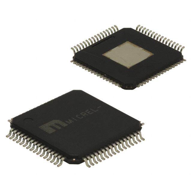
| 描述 | IC CLK TRANSLATOR PLL 72-LFCSP时钟发生器及支持产品 Dual PLL Quad In Mltservice Line Card |
| DevelopmentKit | AD9559/PCBZ |
| 产品分类 | |
| 品牌 | Analog Devices Inc |
| 产品手册 | |
| 产品图片 | |
| rohs | 符合RoHS无铅 / 符合限制有害物质指令(RoHS)规范要求 |
| 产品系列 | 时钟和计时器IC,时钟发生器及支持产品,Analog Devices AD9559BCPZ- |
| 数据手册 | |
| 产品型号 | AD9559BCPZ |
| PLL | 是 |
| 主要用途 | 以太网,SONET/SDH,Stratum |
| 产品种类 | 时钟发生器及支持产品 |
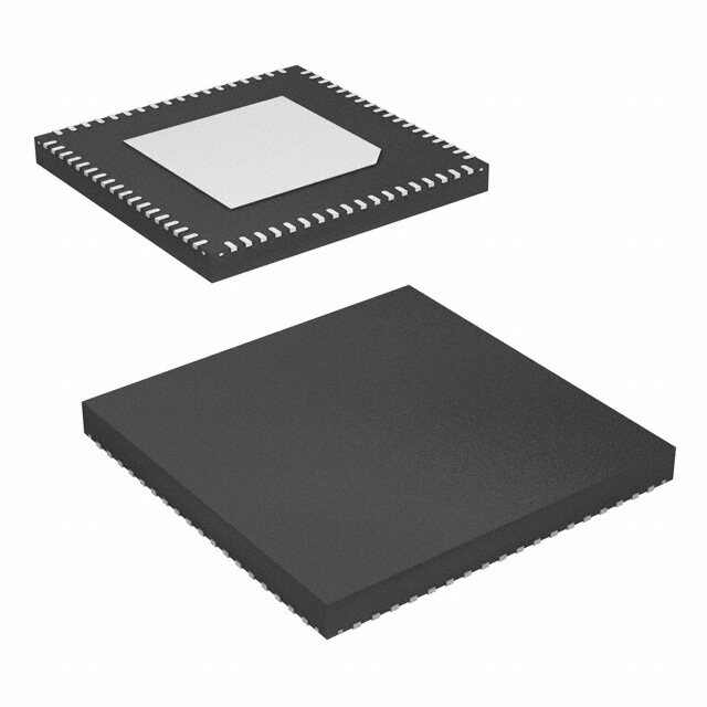
| 供应商器件封装 | 72-LFCSP-VQ(10x10) |
| 包装 | 托盘 |
| 商标 | Analog Devices |
| 安装类型 | 表面贴装 |
| 安装风格 | SMD/SMT |
| 封装 | Tray |
| 封装/外壳 | 72-VFQFN 裸露焊盘,CSP |
| 封装/箱体 | LFCSP-72 |
| 工作温度 | -40°C ~ 85°C |
| 工作电源电压 | 3.3 V |
| 工厂包装数量 | 168 |
| 差分-输入:输出 | 是/是 |
| 最大工作温度 | + 85 C |
| 最大输入频率 | 1250 MHz |
| 最大输出频率 | 1250 MHz |
| 最小工作温度 | - 40 C |
| 标准包装 | 1 |
| 比率-输入:输出 | 4:4 |
| 电压-电源 | 1.71 V ~ 3.465 V |
| 电路数 | 1 |
| 系列 | AD9559 |
| 输入 | LVDS,LVPECL |
| 输出 | CMOS,HSTL,LVDS |
| 输出端数量 | 4 |
| 输出类型 | LVDS |
| 频率-最大值 | 1.25GHz |


- 商务部:美国ITC正式对集成电路等产品启动337调查
- 曝三星4nm工艺存在良率问题 高通将骁龙8 Gen1或转产台积电
- 太阳诱电将投资9.5亿元在常州建新厂生产MLCC 预计2023年完工
- 英特尔发布欧洲新工厂建设计划 深化IDM 2.0 战略
- 台积电先进制程称霸业界 有大客户加持明年业绩稳了
- 达到5530亿美元!SIA预计今年全球半导体销售额将创下新高
- 英特尔拟将自动驾驶子公司Mobileye上市 估值或超500亿美元
- 三星加码芯片和SET,合并消费电子和移动部门,撤换高东真等 CEO
- 三星电子宣布重大人事变动 还合并消费电子和移动部门
- 海关总署:前11个月进口集成电路产品价值2.52万亿元 增长14.8%

PDF Datasheet 数据手册内容提取
Dual PLL, Quad Input, Multiservice Line Card Adaptive Clock Translator Data Sheet AD9559 FEATURES Pin program function for easy frequency translation configuration Supports GR-1244 Stratum 3 stability in holdover mode Software controlled power-down Supports smooth reference switchover with virtually 72-lead (10 mm × 10 mm) LFCSP package no disturbance on output phase Supports Telcordia GR-253 jitter generation, transfer, and APPLICATIONS tolerance for SONET/SDH up to OC-192 systems Network synchronization, including synchronous Ethernet Supports ITU-T G.8262 synchronous Ethernet slave clocks and SDH to OTN mapping/demapping Supports ITU-T G.823, G.824, G.825, and G.8261 Cleanup of reference clock jitter Auto/manual holdover and reference switchover SONET/SDH clocks up to OC-192, including FEC Adaptive clocking allows dynamic adjustment of feedback Stratum 3 holdover, jitter cleanup, and phase transient dividers for use in OTN mapping/demapping applications control Dual digital PLL architecture with four reference inputs Wireless base station controllers (single-ended or differential) Cable infrastructure 4x2 crosspoint allows any reference input to drive either PLL Data communications Input reference frequencies from 2 kHz to 1250 MHz Reference validation and frequency monitoring (2 ppm) GENERAL DESCRIPTION Programmable input reference switchover priority The AD9559 is a low loop bandwidth clock multiplier that 20-bit programmable input reference divider provides jitter cleanup and synchronization for many systems, 4 pairs of clock output pins with each pair configurable as a including synchronous optical networks (SONET/SDH). The single differential LVDS/HSTL output or as 2 single-ended AD9559 generates an output clock synchronized to up to four CMOS outputs external input references. The digital PLL allows for reduction Output frequencies: 262 kHz to 1250 MHz of input time jitter or phase noise associated with the external Programmable 17-bit integer and 23-bit fractional references. The digitally controlled loop and holdover circuitry feedback divider in digital PLL of the AD9559 continuously generates a low jitter output clock Programmable digital loop filter covering loop bandwidths even when all reference inputs have failed. from 0.1 Hz to 2 kHz Low noise system clock multiplier The AD9559 operates over an industrial temperature range of Optional crystal resonator for system clock input −40°C to +85°C. If a single DPLL version of this part is needed, On-chip EEPROM to store multiple power-up profiles refer to the AD9557. FUNCTIONAL BLOCK DIAGRAM CHANNEL 0A AD9559 DIVIDER DIGITAL ANALOG ÷3 TO ÷11 CHANNEL 0B PLL 0 PLL 0 HF DIVIDER 0 DIVIDER REFERENCE INPUT DIGITAL ANALOG ÷3 TO ÷11 CHANNEL 1A MONITOR PLL 1 PLL 1 HF DIVIDER 1 DIVIDER AND MUX CLOCK EEPROM MULTIPLIER SERIAL INTERFACE CSOTNATTRUOSL A PNINDS CHDAINVNIDEELR 1B (SPI OR I2C) SSOTUARBCLEE 10644-001 Figure 1. Rev. C Document Feedback Information furnished by Analog Devices is believed to be accurate and reliable. However, no responsibility is assumed by Analog Devices for its use, nor for any infringements of patents or other One Technology Way, P.O. Box 9106, Norwood, MA 02062-9106, U.S.A. rights of third parties that may result from its use. Specifications subject to change without notice. No license is granted by implication or otherwise under any patent or patent rights of Analog Devices. Tel: 781.329.4700 ©2012–2013 Analog Devices, Inc. All rights reserved. Trademarks and registered trademarks are the property of their respective owners. Technical Support www.analog.com
AD9559 Data Sheet TABLE OF CONTENTS Features .............................................................................................. 1 Digital PLL (DPLL) Core .......................................................... 34 Applications ....................................................................................... 1 Loop Control State Machine ..................................................... 36 General Description ......................................................................... 1 System Clock (SYSCLK) ................................................................ 37 Functional Block Diagram .............................................................. 1 SYSCLK Inputs ........................................................................... 37 Revision History ............................................................................... 3 SYSCLK Multiplier ..................................................................... 37 Specifications ..................................................................................... 4 Output PLL (APLL) ....................................................................... 39 Supply Voltage ............................................................................... 4 APLL Configuration .................................................................. 39 Supply Current .............................................................................. 4 APLL Calibration ....................................................................... 39 Power Dissipation ......................................................................... 5 Clock Distribution .......................................................................... 40 System Clock Inputs (XOA, XOB) ............................................. 5 Clock Dividers ............................................................................ 40 Reference Inputs ........................................................................... 6 Output Enable ............................................................................. 40 Reference Monitors ...................................................................... 7 Output Mode and Power-Down .............................................. 40 Reference Switchover Specifications .......................................... 7 Clock Distribution Synchronization ........................................ 41 Distribution Clock Outputs ........................................................ 8 Status and Control .......................................................................... 42 Time Duration of Digital Functions ........................................ 10 Multifunction Pins (M0 to M5) ............................................... 42 Digital PLL (DPLL_0 and DPLL_1) ........................................ 10 IRQ Function .............................................................................. 42 Analog PLL (APLL_0 and APLL_1) ........................................ 10 Watchdog Timer ......................................................................... 43 Digital PLL Lock Detection ...................................................... 10 EEPROM ..................................................................................... 43 Holdover Specifications ............................................................. 10 Serial Control Port ......................................................................... 49 Serial Port Specifications—SPI Mode ...................................... 11 SPI/I²C Port Selection ................................................................ 49 Serial Port Specifications—I2C Mode ...................................... 12 SPI Serial Port Operation .......................................................... 49 Logic Inputs (RESET, M5 to M0) ............................................. 12 I²C Serial Port Operation .......................................................... 53 Logic Outputs (M5 to M0) ........................................................ 12 Programming the I/O Registers ................................................... 56 Jitter Generation ......................................................................... 13 Buffered/Active Registers .......................................................... 56 Absolute Maximum Ratings .......................................................... 16 Write Detect Registers ............................................................... 56 ESD Caution ................................................................................ 16 Autoclear Registers ..................................................................... 56 Pin Configuration and Function Descriptions ........................... 17 Register Access Restrictions...................................................... 56 Typical Performance Characteristics ........................................... 20 Thermal Performance .................................................................... 57 Input/Output Termination Recommendations .......................... 26 Power Supply Partitions ................................................................. 58 Getting Started ................................................................................ 27 3.3 V Supplies .............................................................................. 58 Chip Power Monitor and Startup ............................................. 27 1.8 V Supplies .............................................................................. 58 Multifunction Pins at Reset/Power-Up ................................... 27 Bypass Capacitors for Pin 21 and Pin 33 ................................. 58 Device Register Programming Using a Register Setup File .. 27 Register Map ................................................................................... 59 Register Programming Overview ............................................. 28 Register Map Bit Descriptions ...................................................... 72 Theory of Operation ...................................................................... 31 Serial Control Port Configuration (Register 0x0000 to Register 0x0005) ......................................................................... 72 Overview ...................................................................................... 31 Clock Part Family ID (Register 0x000C and Register 0x000D) 72 Reference Input Physical Connections .................................... 32 User Scratchpad (Register 0x000E and Register 0x000F) ..... 73 Reference Monitors .................................................................... 32 General Configuration (Register 0x0100 to Register 0x0109) .. 73 Reference Input Block ................................................................ 32 IRQ Mask (Register 0x010A to Register 0x112) .................... 74 Reference Switchover ................................................................. 33 Rev. C | Page 2 of 120
Data Sheet AD9559 System Clock (Register 0x0200 to Register 0x0207) .............. 76 DPLL_1 Settings for Reference Input A (REFA) (Register Reference Input A (Register 0x0300 to Register 0x031A) ..... 77 0x055A to Register 0x0566) ....................................................... 98 DPLL_1 Settings for Reference Input B (REFB) (Register Reference Input B (Register 0x0320 to Register 0x033A)...... 78 0x0567 to Register 0x0573) ........................................................ 99 Reference Input C (Register 0x0340 to Register 0x035A) ..... 79 Digital Loop Filter Coefficients (Register 0x0800 to Register Reference Input D (Register 0x0360 to Register 0x037A) ..... 81 0x0817) ....................................................................................... 100 DPLL_0 Controls (Register 0x0400 to Register 0x0415) ....... 82 Common Operational Controls (Register 0x0A00 to Register APLL_0 Configuration (Register 0x0420 to Register 0x0423) .. 84 0x0A0E) ...................................................................................... 101 PLL_0 Output Sync and Clock Distribution (Register 0x0424 PLL_0 Operational Controls (Register 0x0A20 to Register to Register 0x042E) ..................................................................... 85 0x0A24) ...................................................................................... 104 DPLL_0 Settings for Reference Input A (REFA) (Register PLL_1 Operational Controls (Register 0x0A40 to Register 0x0440 to Register 0x044C) ....................................................... 87 0x0A44) ...................................................................................... 106 DPLL_0 Settings for Reference Input B (REFB) (Register Status ReadBack (Register 0x0D00 to Register 0x0D05) ..... 107 0x044D to Register 0x0459) ....................................................... 88 IRQ Monitor (Register 0x0D08 to Register 0x0D10) .......... 108 DPLL_0 Settings for Reference Input C (REFC) (Register PLL_0 Read-Only Status (Register 0x0D20 to Register 0x045A to Register 0x0466) ....................................................... 89 0x0D2A) ..................................................................................... 110 DPLL_0 Settings for Reference Input D (REFD) (Register PLL_1 Read-Only Status (Register 0x0D40 to Register 0x0467 to Register 0x0473) ........................................................ 90 0x0D4A) ..................................................................................... 112 DPLL_1 Controls (Register 0x0500 to Register 0x0515) ....... 91 EEPROM Control (Register 0x0E00 to Register 0x0E03) ... 113 APLL_1 Configuration (Register 0x0520 to Register 0x0523) ... 93 EEPROM Storage Sequence (Register 0x0E10 to Register PLL_1 Output Sync and Clock Distribution (Register 0x0524 0x0E3C) ...................................................................................... 113 to Register 0x052E) ..................................................................... 94 Outline Dimensions ...................................................................... 120 DPLL_1 Settings for Reference Input C (REFC) (Register Ordering Guide ......................................................................... 120 0x0540 to Register 0x054C) ....................................................... 96 DPLL_1 Settings for Reference Input D (REFD) (Register 0x054D to Register 0x0559) ....................................................... 97 REVISION HISTORY 5/13—Rev. B to Rev. C Changes to Table 34 ........................................................................ 63 Changes to Table 91 ........................................................................ 87 Changes to Table 25 ........................................................................ 49 Changes to Table 92, Table 96, and Table 97 ............................... 88 3/13—Rev. A to Rev. B Changes to Table 101 and Table 102 ............................................. 89 Changes to Device Register Programming Using a Register Changes to Table 106 and Table 107 ............................................. 90 Setup File Section ............................................................................ 27 Changes to Table 126 ...................................................................... 97 Changed 101100 to 1101100, Table 25 ......................................... 49 Changes to Table 127, Table 131, and Table 132 ......................... 97 Changes to Table 136 and Table 137 ............................................. 98 12/12—Rev. 0 to Rev. A Changes to Table 141 and Table 142 ............................................. 99 Change to Features Section .............................................................. 1 Changes to Table 179 .................................................................... 113 Changes to DPLL Overview Section, Figure 35, and Updated Outline Dimensions...................................................... 120 Figure 36 ........................................................................................... 34 7/12—Revision 0: Initial Version Changes to EEPROM Upload Section and Manual EEPROM Download Section ........................................................................... 45 Changes to Table 25 ........................................................................ 49 Rev. C | Page 3 of 120
AD9559 Data Sheet SPECIFICATIONS Minimum (min) and maximum (max) values apply for the full range of supply voltage and operating temperature variations. Typical (typ) values apply for VDD3 = 3.3 V; VDD = 1.8 V; T = 25°C, unless otherwise noted. A SUPPLY VOLTAGE Table 1. Parameter Min Typ Max Unit Test Conditions/Comments SUPPLY VOLTAGE VDD3 3.135 3.30 3.465 V VDD 1.71 1.80 1.89 V SUPPLY CURRENT The test conditions for the maximum (max) supply current are at the maximum supply voltage found in Table 1. The test conditions for the typical (typ) supply current are at the typical supply voltage found in Table 1. The test conditions for the minimum (min) supply current are at the minimum supply voltage found in Table 1. Table 2. Parameter Min Typ Max Unit Test Conditions/Comments SUPPLY CURRENT FOR TYPICAL CONFIGURATION Typical values are for the Typical Configuration parameter listed in Table 3 I 34 42 50 mA VDD3 I 253 316 380 mA VDD SUPPLY CURRENT FOR ALL BLOCKS RUNNING Maximum values are for the All Blocks Running CONFIGURATION parameter listed in Table 3 I 75 94 113 mA VDD3 I 256 320 384 mA VDD Rev. C | Page 4 of 120
Data Sheet AD9559 POWER DISSIPATION Table 3. Parameter Min Typ Max Unit Test Conditions/Comments POWER DISSIPATION Typical Configuration 0.57 0.71 0.85 W System clock: 49.152 MHz crystal; two DPLLs active; two 19.44 MHz input references in differential mode; two HSTL drivers at 644.53125 MHz; two 3.3 V CMOS drivers at 161.1328125 MHz and 80 pF capacitive load on CMOS output All Blocks Running 0.71 0.89 1.1 W System clock: 49.152 MHz crystal; two DPLLs active, all input references in differential mode; two HSTL drivers at 750 MHz; four 3.3 V CMOS drivers at 250 MHz and 80 pF capacitive load on CMOS outputs Full Power-Down 75 110 mW Typical configuration with no external pull-up or pull- down resistors; about 2/3 of this power is on VDD3 Incremental Power Dissipation Typical configuration; table values show the change in power due to the indicated operation Complete DPLL/APLL On/Off 171 214 257 mW This power delta is computed relative to the typical configuration; the blocks powered down include one reference input, one DPLL, one APLL, one P divider, two channel dividers, one HSTL driver, and one CMOS driver; roughly 2/3 of the power savings is on the 1.8 V supply Input Reference On/Off Differential Without Divide-by-2 19 25 31 mW Additional current draw is in the VDD3 domain only Differential With Divide-by-2 25 32 39 mW Additional current draw is in the VDD3 domain only Single-Ended (Without Divide-by-2) 5 6.6 8 mW Additional current draw is in the VDD3 domain only Output Distribution Driver On/Off LVDS (at 750 MHz) 12 17 22 mW Additional current draw is in the VDD domain only HSTL (at 750 MHz) 14 21 28 mW Additional current draw is in the VDD domain only 1.8 V CMOS (at 250 MHz) 14 21 28 mW A single 1.8 V CMOS output with an 80 pF load 3.3 V CMOS (at 250 MHz) 18 27 36 mW A single 3.3 V CMOS output with an 80 pF load SYSTEM CLOCK INPUTS (XOA, XOB) Table 4. Parameter Min Typ Max Unit Test Conditions/Comments SYSTEM CLOCK MULTIPLIER PLL Output Frequency Range 750 805 MHz VCO range may place limitations on nonstandard system clock input frequencies Phase Frequency Detector (PFD) Rate 150 MHz Frequency Multiplication Range 4 255 Assumes valid system clock and PFD rates SYSTEM CLOCK REFERENCE INPUT PATH Input Frequency Range 10 400 MHz Minimum Input Slew Rate 50 V/μs Minimum limit imposed for jitter performance; jitter performance affected if sine wave input ≤ 20 MHz Common-Mode Voltage 1.05 1.16 1.27 V Internally generated Differential Input Voltage Sensitivity 250 mV p-p Minimum voltage across pins required to ensure switching between logic states; the instantaneous voltage on either pin must not exceed supply rails; single-ended input can be accommodated by ac grounding complementary input; 1 V p-p recommended for optimal jitter performance System Clock Input Doubler Duty Cycle Amount of duty cycle variation that can be tolerated on the system clock input to use the doubler System Clock input = 50 MHz 45 50 55 % System Clock input = 20 MHz 46 50 54 % System Clock input = 16 MHz to 20 MHz 47 50 53 % Input Capacitance 3 pF Single-ended, each pin Input Resistance 4.1 kΩ Rev. C | Page 5 of 120
AD9559 Data Sheet Parameter Min Typ Max Unit Test Conditions/Comments CRYSTAL RESONATOR PATH Crystal Resonator Frequency Range 10 50 MHz Fundamental mode, AT cut crystal Maximum Crystal Motional Resistance 100 Ω REFERENCE INPUTS Table 5. Parameter Min Typ Max Unit Test Conditions/Comments DIFFERENTIAL OPERATION Frequency Range The reference input divide-by-2 block must be engaged for f > 705 MHz IN Sinusoidal Input 10 750 MHz LVPECL Input 0.002 1250 MHz LVDS Input 0.002 750 MHz Minimum Input Slew Rate 40 V/μs Minimum limit imposed for jitter performance Common-Mode Input Voltage AC-Coupled 1.9 2 2.1 V Internally generated DC-Coupled 1.0 2.4 V Differential Input Voltage Sensitivity mV Minimum differential voltage across pins required to ensure switching between logic levels; instantaneous voltage on either pin must not exceed the supply rails f < 800 MHz 240 mV IN f = 800 MHz to 1050 MHz 320 mV IN f = 1050 MHz to 1250 MHz 400 mV IN Differential Input Voltage Hysteresis 55 100 mV Input Resistance 21 kΩ Input Capacitance 3 pF Minimum Pulse Width High LVPECL 390 ps LVDS 640 ps Minimum Pulse Width Low LVPECL 390 ps LVDS 640 ps SINGLE-ENDED OPERATION Frequency Range (CMOS) 0.002 300 MHz Minimum Input Slew Rate 40 V/μs Minimum limit imposed for jitter performance Input Voltage High (V ) IH 1.2 V to 1.5 V Threshold Setting 1.0 V 1.8 V to 2.5 V Threshold Setting 1.4 V 3.0 V to 3.3 V Threshold Setting 2.0 V Input Voltage Low (V ) IL 1.2 V to 1.5 V Threshold Setting 0.35 V 1.8 V to 2.5 V Threshold Setting 0.5 V 3.0 V to 3.3 V Threshold Setting 1.0 V Input Resistance 47 kΩ Input Capacitance 3 pF Minimum Pulse Width High 1.5 ns Minimum Pulse Width Low 1.5 ns Rev. C | Page 6 of 120
Data Sheet AD9559 REFERENCE MONITORS Table 6. Parameter Min Typ Max Unit Test Conditions/Comments REFERENCE MONITORS Reference Monitor Loss of Reference Detection Time 1.15 DPLL PFD Nominal phase detector period = R/f 1 REF period Frequency Out-of Range Limits 2 105 Δf/f Programmable (lower bound subject to quality REF (ppm) of the system clock (SYSCLK)); SYSCLK accuracy must be less than the lower bound Validation Timer 0.001 65.535 sec Programmable in 1 ms increments 1 fREF is the frequency of the active reference; R is the frequency division factor determined by the R divider. REFERENCE SWITCHOVER SPECIFICATIONS Table 7. Parameter Min Typ Max Unit Test Conditions/Comments REFERENCE SWITCHOVER SPECIFICATIONS Assumes a jitter-free reference; satisfies Maximum Output Phase Perturbation Telcordia GR-1244-CORE requirements; (Phase Build-Out Switchover) base loop filter selection bit set to 1b for all active references 50 Hz DPLL Loop Bandwidth Test conditions: 19.44 MHz to 174.70308 MHz; DPLL BW = 50 Hz; 49.152 MHz signal generator used for system clock source Peak ±55 ±100 ps Steady State ±55 ±100 ps Time Required to Switch to a New Reference Phase Build-Out Switchover 10 DPLL PFD Calculated using the nominal phase detector period period (NPDP = R/fREF); the total time required is the time plus the reference validation time, plus the time required to lock to the new reference Rev. C | Page 7 of 120
AD9559 Data Sheet DISTRIBUTION CLOCK OUTPUTS Table 8. Parameter Min Typ Max Unit Test Conditions/Comments HSTL MODE Output Frequency OUT0A, OUT0A and OUT0B, OUT0B 0.262 1250 MHz OUT1A, OUT1A and OUT1B, OUT1B 0.302 1250 MHz Rise/Fall Time (20% to 80%)1 140 250 ps 100 Ω termination across the output pair Duty Cycle Up to f = 700 MHz 44 48 53 % OUT Up to f = 750 MHz 43 48 54 % OUT Up to f = 1250 MHz 43 % OUT Differential Output Voltage Swing 700 925 1200 mV Magnitude of voltage across pins; output driver static Common-Mode Output Voltage 750 850 1000 mV Output driver static Reference Input-to-Output Delay Variation 3.2 ps/°C HSTL mode; DPLL locked to same input over Temperature reference at all times; stable system clock source (non-XTAL) Static Phase Offset Variation from Active 0.875 ps/mV Valid for HSTL, LVDS, and 1.8 V CMOS output Reference to Output over Voltage driver modes Extremes LVDS MODE Output Frequency OUT0A, OUT0A and OUT0B, OUT0B 0.262 1250 MHz OUT1A, OUT1A and OUT1B, OUT1B 0.302 1250 MHz Rise/Fall Time (20% to 80%)1 185 280 ps 100 Ω termination across the output pair Duty Cycle Up to f = 750 MHz 43 48 53 % OUT Up to f = 800 MHz 42.5 48 53.5 % OUT Up to f = 1250 MHz 43 % OUT Differential Output Voltage Swing Balanced, V 247 454 mV Voltage swing between output pins; output OD driver static Unbalanced, ΔV 50 mV Absolute difference between voltage swing of OD normal pin and inverted pin; output driver static Offset Voltage Common Mode, V 1.125 1.25 1.375 V Output driver static OS Common-Mode Difference, ΔV 50 mV Voltage difference between pins; output driver OS static Short-Circuit Output Current 10 24 mA Output driver static CMOS MODE Output Frequency 1.8 V Supply OUT0A, OUT0A and OUT0B, OUT0B 0.262 250 MHz 10 pF load OUT1A, OUT1A and OUT1B, OUT1B 0.302 250 MHz 10 pF load 3.3 V Supply (OUT0A and OUT1A) Strong Drive Strength Setting OUT0A, OUT0A 0.262 250 MHz 10 pF load OUT1A, OUT1A 0.302 250 MHz 10 pF load Weak Drive Strength Setting OUT0A, OUT0A 0.262 25 MHz 10 pF load OUT1A, OUT1A 0.302 25 MHz 10 pF load Rev. C | Page 8 of 120
Data Sheet AD9559 Parameter Min Typ Max Unit Test Conditions/Comments Rise/Fall Time (20% to 80%)1 1.8 V Mode 1.5 3 ns 10 pF load 3.3 V Strong Mode 0.4 0.6 ns 10 pF load 3.3 V Weak Mode 8 ns 10 pF load Duty Cycle 1.8 V Mode 50 % 10 pF load 3.3 V Strong Mode 47 51 56 % 10 pF load 3.3 V Weak Mode 51 % 10 pF load Output Voltage High (V ) Output driver static; strong drive strength OH VDD3 = 3.3 V, I = 10 mA VDD3 − 0.3 V OH VDD3 = 3.3 V, I = 1 mA VDD3 − 0.1 V OH VDD3 = 1.8 V, I = 1 mA VDD − 0.2 V OH Output Voltage Low (V ) Output driver static; strong drive strength OL VDD3 = 3.3 V, I = 10 mA 0.3 V OL VDD3 = 3.3 V, I = 1 mA 0.1 V OL VDD3 = 1.8 V, I = 1 mA 0.1 V OL OUTPUT TIMING SKEW 10 pF load Between OUT0A, OUT0A and OUT0B, OUT0B 116 265 ps HSTL mode on both drivers; rising edge only; or OUT1A, OUT1A and OUT1B, OUT1B any divide value Additional Delay on One Driver by Changing Its Logic Type HSTL to LVDS 0 +15 +35 ps Positive value indicates that the LVDS edge is delayed relative to HSTL HSTL to 1.8 V CMOS −5 0 +5 ps Positive value indicates that the CMOS edge is delayed relative to HSTL OUT0B, OUT0B HSTL to OUT0B, OUT0B −765 −280 +250 ns The CMOS edge is delayed relative to HSTL 3.3 V CMOS, Strong Mode OUT1B, OUT1B HSTL to OUT1B, OUT1B −765 −280 +250 ns The CMOS edge is delayed relative to HSTL 3.3 V CMOS, Strong Mode 1 The listed values are for the slower edge (rising or falling). Rev. C | Page 9 of 120
AD9559 Data Sheet TIME DURATION OF DIGITAL FUNCTIONS Table 9. Parameter Min Typ Max Unit Test Conditions/Comments TIME DURATION OF DIGITAL FUNCTIONS EEPROM-to-Register Download Time 16 25 ms Uses default EEPROM storage sequence (see Register 0x0E10 to Register 0x0E4F) Register-to-EEPROM Upload Time 180 ms Uses default EEPROM storage sequence (see Register 0x0E10 to Register 0x0E4F Power-Down Exit Time 1 ms Time from power-down exit to system clock lock detect; system clock stability timer setting should be added to calculate the time needed for system clock stable DIGITAL PLL (DPLL_0 AND DPLL_1) Table 10. Parameter Min Typ Max Unit Test Conditions/Comments DIGITAL PLL Phase Frequency Detector (PFD) Input 2 100 kHz Frequency Range Loop Bandwidth 0.1 2000 Hz Programmable design parameter; note that (f /loop BW) ≥ 20 PFD Phase Margin 45 89 Degrees Programmable design parameter Closed Loop Peaking <0.1 dB Programmable design parameter; part can be programmed for <0.1 dB peaking in accordance with Telcordia GR-253-CORE jitter transfer ANALOG PLL (APLL_0 AND APLL_1) Table 11. Parameter Min Typ Max Unit Test Conditions/Comments ANALOG PLL0 VCO Frequency Range 2940 3543 MHz Phase Frequency Detector (PFD) Input 180 195 MHz Frequency Range Loop Bandwidth 240 kHz Programmable design parameter Phase Margin 68 Degrees Programmable design parameter ANALOG PLL1 VCO Frequency Range 3405 4260 MHz Phase Frequency Detector (PFD) Input 180 195 MHz Frequency Range Loop Bandwidth 240 kHz Programmable design parameter Phase Margin 68 Degrees Programmable design parameter DIGITAL PLL LOCK DETECTION Table 12. Parameter Min Typ Max Unit Test Conditions/Comments PHASE LOCK DETECTOR Threshold Programming Range 10 224 − 1 ps Reference-to-feedback phase difference Threshold Resolution 1 ps FREQUENCY LOCK DETECTOR Threshold Programming Range 10 224 − 1 ps Reference-to-feedback period difference Threshold Resolution 1 ps HOLDOVER SPECIFICATIONS Table 13. Parameter Min Typ Max Unit Test Conditions/Comments HOLDOVER SPECIFICATIONS Initial Frequency Accuracy <0.01 ppm Excludes frequency drift of SYSCLK source; excludes frequency drift of input reference prior to entering holdover; compliant with GR-1244 Stratum 3 Rev. C | Page 10 of 120
Data Sheet AD9559 SERIAL PORT SPECIFICATIONS—SPI MODE Table 14. Parameter Min Typ Max Unit Test Conditions/Comments M5/CS M5/CS is a dual function pin; the values in this table apply when this pin is used as a serial port pin, that is, CS; see Table 16 for the specifications when this pin is used as a multifunction pin (M5) Input Logic 1 Voltage 2.2 V Input Logic 0 Voltage 0.8 V Input Logic 1 Current 20 µA Input Logic 0 Current 50 µA Input Capacitance 2 pF SCLK Internal 10 kΩ pull-down resistor Input Logic 1 Voltage 2.2 V Input Logic 0 Voltage 0.8 V Input Logic 1 Current 200 µA Input Logic 0 Current 1 µA Input Capacitance 2 pF SDIO As an Input Input Logic 1 Voltage 2.2 V Input Logic 0 Voltage 0.8 V Input Logic 1 Current 1 µA Input Logic 0 Current 1 µA Input Capacitance 2 pF As an Output Output Logic 1 Voltage VDD3 − 0.6 V 1 mA load current Output Logic 0 Voltage 0.4 V 1 mA load current M4/SDO M4/SDO is a dual function pin; the values in this table apply when this pin is used as a serial port pin, that is SDO; see Table 16 for the specifications when this pin is used as a multifunction pin (M4) Output Logic 1 Voltage VDD3 − 0.6 V 1 mA load current Output Logic 0 Voltage 0.4 V 1 mA load current TIMING See Figure 47 and Figure 50 SCLK Clock Rate, 1/t 40 MHz CLK Pulse Width High, t 10 ns HIGH Pulse Width Low, t 13 ns LOW SDIO to SCLK Setup, t 3 ns DS SCLK to SDIO Hold, t 6 ns DH SCLK to Valid SDIO and SDO, t 10 ns DV CS to SCLK Setup (tS) 10 ns CS to SCLK Hold (tC) 0 ns CS Minimum Pulse Width High 6 ns Rev. C | Page 11 of 120
AD9559 Data Sheet SERIAL PORT SPECIFICATIONS—I2C MODE Table 15. Parameter Min Typ Max Unit Test Conditions/Comments SDA, SCL (AS INPUTS) Input Logic 1 Voltage 0.7 × VDD3 V Input Logic 0 Voltage 0.3 × VDD3 V Input Current −10 +10 µA For V = 10% to 90% of VDD3 IN Hysteresis of Schmitt Trigger Inputs 0.015 × VDD3 Pulse Width of Spikes That Must Be Suppressed 50 ns by the Input Filter, t SP SDA (AS OUTPUT) Output Logic 0 Voltage 0.4 V I = 3 mA O Output Fall Time from V to V 20 + 0.1 C 1 250 ns 10 pF ≤ C ≤ 400 pF IHmin ILmax b b TIMING SCL Clock Rate 400 kHz Bus-Free Time Between a Stop and Start 1.3 µs Condition, t BUF Repeated Start Condition Setup Time, t 0.6 µs SU; STA Repeated Hold Time Start Condition, t 0.6 µs After this period, the first clock pulse is HD; STA generated Stop Condition Setup Time, t 0.6 µs SU; STO Low Period of the SCL Clock, t 1.3 µs LOW High Period of the SCL Clock, t 0.6 µs HIGH SCL/SDA Rise Time, tR 20 + 0.1 Cb1 300 ns SCL/SDA Fall Time, tF 20 + 0.1 Cb1 300 ns Data Setup Time, t 100 ns SU; DAT Data Hold Time, t 100 ns HD; DAT Capacitive Load for Each Bus Line, C1 400 pF b 1 Cb is the capacitance (pF) of a single bus line. LOGIC INPUTS (RESET, M5 TO M0) Table 16. Parameter Min Typ Max Unit Test Conditions/Comments RESET PIN Input High Voltage (V ) 2.1 V IH Input Low Voltage (V ) 0.8 V IL Input Current (I , I ) ±85 ±125 µA INH INL Input Capacitance (C ) 3 pF IN LOGIC INPUTS (M5 to M0) The M4 and M5 pins are dual function pins; the values in this table apply when M4/SDO and M5/CS are used as M pins; see Table 14 in the Serial Port Specifications—SPI Mode section for the specifications when these pins are used as serial port pins (SDO, CS) Input High Voltage (V ) 2.5 V IH Input Low Voltage (V ) 0.6 V IL Input Current (I , I ) ±1 ±5 µA INH INL Input Capacitance (C ) 3 pF IN LOGIC OUTPUTS (M5 TO M0) Table 17. Parameter Min Typ Max Unit Test Conditions/Comments LOGIC OUTPUTS (M5 to M0) Output High Voltage (V ) VDD3 − 0.4 V I = 1 mA OH OH Output Low Voltage (V ) 0.4 V I = 1 mA OL OL Rev. C | Page 12 of 120
Data Sheet AD9559 JITTER GENERATION Jitter Generation (Random Jitter)—49.152 MHz Crystal for System Clock Input Table 18. Parameter Min Typ Max Unit Test Conditions/Comments JITTER GENERATION System clock doubler enabled. High phase margin mode enabled. Both PLLs are running with same output frequency. In cases where the two PLLs have different jitter, the higher jitter is listed. When two driver types are listed, both were tested at those conditions; the driver type with higher jitter is quoted, although there is usually not a significant jitter difference between driver types. f = 19.44 MHz; f = 622.08 MHz; f = 50 Hz; REF OUT LOOP HSTL Driver Bandwidth: 5 kHz to 20 MHz 307 fs rms Bandwidth: 12 kHz to 20 MHz 310 fs rms Bandwidth: 20 kHz to 80 MHz 313 fs rms Bandwidth: 50 kHz to 80 MHz 292 fs rms Bandwidth: 16 MHz to 320 MHz 149 fs rms f = 19.44 MHz; f = 644.53 MHz; f = 50 Hz; REF OUT LOOP HSTL Driver, LVDS Driver Bandwidth: 5 kHz to 20 MHz 313 fs rms Bandwidth: 12 kHz to 20 MHz 306 fs rms Bandwidth: 20 kHz to 80 MHz 308 fs rms Bandwidth: 50 kHz to 80 MHz 286 fs rms Bandwidth: 16 MHz to 320 MHz 154 fs rms f = 19.44 MHz; f = 693.48 MHz; f = 50 Hz; REF OUT LOOP HSTL Driver Bandwidth: 5 kHz to 20 MHz 335 fs rms Bandwidth: 12 kHz to 20 MHz 328 fs rms Bandwidth: 20 kHz to 80 MHz 328 fs rms Bandwidth: 50 kHz to 80 MHz 298 fs rms Bandwidth: 16 MHz to 320 MHz 150 fs rms f = 19.44 MHz; f = 174.703 MHz; f = 1 kHz; REF OUT LOOP HSTL Driver Bandwidth: 5 kHz to 20 MHz 396 fs rms Bandwidth: 12 kHz to 20 MHz 335 fs rms Bandwidth: 20 kHz to 80 MHz 369 fs rms Bandwidth: 50 kHz to 80 MHz 347 fs rms Bandwidth: 4 MHz to 80 MHz 230 fs rms f = 19.44 MHz; f = 174.703 MHz; f = 100 Hz; REF OUT LOOP LVDS Driver, 3.3 V CMOS Driver Bandwidth: 5 kHz to 20 MHz 337 fs rms Bandwidth: 12 kHz to 20 MHz 330 fs rms Bandwidth: 20 kHz to 80 MHz 354 fs rms Bandwidth: 50 kHz to 80 MHz 339 fs rms Bandwidth: 4 MHz to 80 MHz 220 fs rms f = 25 MHz; f = 161.1328 MHz; f = 100 Hz; REF OUT LOOP HSTL Driver Bandwidth: 5 kHz to 20 MHz 318 fs rms Bandwidth: 12 kHz to 20 MHz 310 fs rms Bandwidth: 20 kHz to 80 MHz 384 fs rms Bandwidth: 50 kHz to 80 MHz 361 fs rms Bandwidth: 4 MHz to 80 MHz 267 fs rms Rev. C | Page 13 of 120
AD9559 Data Sheet Parameter Min Typ Max Unit Test Conditions/Comments f = 2 kHz; f = 70.656 MHz; f = 100 Hz; REF OUT LOOP HSTL Driver, 3.3 V CMOS Driver Bandwidth: 10Hz to 30 MHz 6.5 ps rms Bandwidth: 5 kHz to 20 MHz 343 fs rms Bandwidth: 12 kHz to 20 MHz 335 fs rms Bandwidth: 10 kHz to 400 kHz 243 fs rms Bandwidth: 100 kHz to 10 MHz 256 fs rms f = 25 MHz; f = 1 GHz; f = 500 Hz; REF OUT LOOP HSTL Driver Bandwidth: 100 Hz to 500 MHz (Broadband) 881 fs rms Bandwidth: 12 kHz to 20 MHz 331 fs rms Bandwidth: 20 kHz to 80 MHz 330 fs rms Jitter Generation (Random Jitter)—19.2 MHz TCXO for System Clock Input Table 19. Parameter Min Typ Max Unit Test Conditions/Comments JITTER GENERATION System clock doubler enabled. High phase margin mode enabled. Both PLLs are running with same output frequency. In cases where the two PLLs have different jitter, the higher jitter is listed. Where two driver types are listed, both were tested at those conditions; the driver type with higher jitter is quoted, although there is usually not a significant jitter difference between driver types. f = 19.44 MHz; f = 644.53 MHz; f = 10 Hz; REF OUT LOOP HSTL Driver Bandwidth: 5 kHz to 20 MHz 380 fs rms Bandwidth: 12 kHz to 20 MHz 373 fs rms Bandwidth: 20 kHz to 80 MHz 373 fs rms Bandwidth: 50 kHz to 80 MHz 348 fs rms Bandwidth: 16 MHz to 320 MHz 148 fs rms f = 19.44 MHz; f = 693.48 MHz; f = 10 Hz; REF OUT LOOP HSTL Driver Bandwidth: 5 kHz to 20 MHz 390 fs rms Bandwidth: 12 kHz to 20 MHz 383 fs rms Bandwidth: 20 kHz to 80 MHz 382 fs rms Bandwidth: 50 kHz to 80 MHz 350 fs rms Bandwidth: 16 MHz to 320 MHz 144 fs rms f = 19.44 MHz; f = 312.5 MHz; f = 10 Hz; REF OUT LOOP HSTL Driver Bandwidth: 5 kHz to 20 MHz 398 fs rms Bandwidth: 12 kHz to 20 MHz 392 fs rms Bandwidth: 20 kHz to 80 MHz 400 fs rms Bandwidth: 50 kHz to 80 MHz 379 fs rms Bandwidth: 4 MHz to 80 MHz 172 fs rms f = 25 MHz; f = 161.1328 MHz; f = 10 Hz; REF OUT LOOP HSTL Driver Bandwidth: 5 kHz to 20 MHz 384 fs rms Bandwidth: 12 kHz to 20 MHz 378 fs rms Bandwidth: 20 kHz to 80 MHz 416 fs rms Bandwidth: 50 kHz to 80 MHz 396 fs rms Bandwidth: 4 MHz to 80 MHz 223 fs rms Rev. C | Page 14 of 120
Data Sheet AD9559 Parameter Min Typ Max Unit Test Conditions/Comments f = 2 kHz; f = 70.656 MHz; f = 10 Hz; REF OUT LOOP HSTL Driver, 3.3 V CMOS Driver Bandwidth: 10 Hz to 30 MHz 3.19 ps rms Bandwidth: 12 kHz to 20 MHz 418 fs rms Bandwidth: 10 kHz to 400 kHz 339 fs rms Bandwidth: 100 kHz to 10 MHz 348 fs rms Rev. C | Page 15 of 120
AD9559 Data Sheet ABSOLUTE MAXIMUM RATINGS Table 20. Stresses above those listed under Absolute Maximum Ratings Parameter Rating may cause permanent damage to the device. This is a stress 1.8 V Supply Voltage (VDD) 2 V rating only; functional operation of the device at these or any 3.3 V Supply Voltage (VDD3) 3.6 V other conditions above those indicated in the operational Maximum Digital Input Voltage −0.5 V to VDD3 + 0.5 V section of this specification is not implied. Exposure to absolute Storage Temperature Range −65°C to +150°C maximum rating conditions for extended periods may affect Operating Temperature Range −40°C to +85°C device reliability. Lead Temperature 300°C ESD CAUTION (Soldering 10 sec) Junction Temperature 150°C Rev. C | Page 16 of 121
Data Sheet AD9559 PIN CONFIGURATION AND FUNCTION DESCRIPTIONS D3FBFBDDDDDABDDDDDFDFDD3 DEEDDDDDOODDDDDEED VRRVVVVVXXVVVVVRRV 210987654321098765 777666666666655555 VDD3 1 PIN 1 54 VDD3 REFA 2 INDICATOR 53 REFC REFA 3 52 REFC VDD 4 51 VDD VDD 5 50 VDD GND 6 49 GND VDD 7 48 VDD VDD 8 AD9559 47 VDD VDD 9 TOP VIEW 46 VDD LDO_0 10 (Not to Scale) 45 LDO_1 LF_011 44 LF_1 VDD3 12 43 VDD3 VDD 13 42 VDD VDD 14 41 VDD OUT0A 15 40 OUT1A OUT0A 16 39 OUT1A VDD 17 38 VDD VDD3 18 37 VDD3 901234567890123456 122222222223333333 BBDDTLASO33210DDBB OUT0OUT0VDGNRESECLK/SCDIO/SDM5/CM4/SDVDDMMMMGNVDOUT1OUT1 SS NOTES 1.THE EXPOSED PAD IS THE GROUND CONNECTION ON THE CHIP. ITNTOO M IESUNESS,T AU BNREDE SPMORELOCDPHEEARRNE IFCDUA TNLOC S TTTIHOREEN NAAGLNITATHLY O BAGEN NDGE RHFOEITUASNT. DD IOSFS ITPHAET IPOCNB, 10644-002 Figure 2. Pin Configuration Table 21. Pin Function Descriptions Input/ Pin No. Mnemonic Output Pin Type Description 1, 12, 18, 28, VDD3 I Power 3.3 V Power Supply. See the Power Supply Partitions section for information about 37, 43, 54, 55, the recommended grouping of the power supply pins. 72 2 REFA I Differential Reference A Input. This internally biased input is typically ac-coupled; when input configured in this manner, it can accept any differential signal with single-ended swing up to 3.3 V. If dc-coupled, input can be LVPECL, LVDS, or single-ended CMOS. 3 REFA I Differential Complementary Reference A Input. Complementary signal to the input provided input on Pin 2. 4, 5, 7, 8, 9, 13, VDD I Power 1.8 V Power Supply. See the Power Supply Partitions section for information about 14, 17, 21, 34, the recommended grouping of the power supply pins. 38, 41, 42, 46, Note that, for Pin 34 and Pin 21, it is recommended that a Size 0201, 0.1 µF bypass 47, 48, 50, 51, capacitor be placed between Pin 33 and Pin 34, as well as between Pin 21 and Pin 22, 58, 59, 60, 61, as close as possible to the AD9559. 62, 65, 66, 67, 68, 69 6, 22, 33, 49 GND O Ground Connect these pins (along with the exposed die pad) to ground. 10 LDO_0 I LDO bypass Output PLL0 Loop Filter Voltage Regulator. Connect a 0.47 μF capacitor from this pin to ground. This pin is also the ac ground reference for the integrated output PLL external loop filter. 11 LF_0 I/O Loop filter for Loop Filter Node for the Output PLL0. Connect an external 6.8 nF capacitor from APLL_0 this pin to Pin 10 (LDO_0). 15 OUT0A O HSTL, LVDS, PLL0 Complementary Output 0A. This output can be configured as HSTL, LVDS, or 1.8 V CMOS single-ended 1.8 V CMOS. 16 OUT0A O HSTL, LVDS, PLL0 Output 0A. This output can be configured as HSTL, LVDS, or single-ended 1.8 V CMOS 1.8 V CMOS. LVPECL levels can be achieved by ac-coupling and using the Thevenin-equivalent termination as described in the Input/Output Termination Recommendations section. Rev. C | Page 17 of 120
AD9559 Data Sheet Input/ Pin No. Mnemonic Output Pin Type Description 19 OUT0B O HSTL, LVDS, PLL0 Complementary Output 0B. This output can be configured as HSTL, LVDS, 1.8 V CMOS, or single-ended 1.8 V or 3.3 V CMOS. 3.3 V CMOS 20 OUT0B O HSTL, LVDS, PLL0 Output 0B. This output can be configured as HSTL, LVDS, or single-ended 1.8 V 1.8 V CMOS, or 3.3 V CMOS. LVPECL levels can be achieved by ac-coupling and using the 3.3 V CMOS Thevenin-equivalent termination as described in the Input/Output Termination Recommendations section. 23 RESET I 3.3 V CMOS Chip Reset. When this active low pin is asserted, the chip goes into reset. This pin Logic has an internal 50 kΩ pull-up resistor. 24 SCLK/SCL I 3.3 V CMOS Serial Programming Clock in SPI Mode (SCLK). Data clock for serial programming. Serial Clock Pin in I2C Mode (SCL). 25 SDIO/SDA I/O 3.3 V CMOS Serial Data Input/Output (SDIO). When the device is in 4-wire SPI mode, data is written via this pin. In 3-wire SPI mode, data reads and writes both occur on this pin. There is no internal pull-up/pull-down resistor on this pin. Serial Data Pin in I2C Mode (SDA). 26 M5/CS I/O 3.3 V CMOS Configurable I/O Pin (M5). Used for status and control of the AD9559. Chip Select in SPI Mode (CS). Active low input. When programming a device in SPI, this pin must be held low. In systems where more than one AD9559 is present, this pin enables individual programming of each AD9559. This pin has an internal 10 kΩ pull-up resistor. 27 M4/SDO I/O 3.3 V CMOS Configurable I/O Pin (M4). Used for status and control of the AD9559. Serial Data Output (SDO). In 4-wire SPI mode, this pin is used for reading serial data. 29, 30, 31, 32 M3, M2, M1, I/O 3.3 V CMOS Configurable I/O Pins. These pins are used for status and control of the AD9559. M0 These pins are also used at power-up and reset to control the serial port configuration and EEPROM loading. See Table 23 and Table 25 for more information. These pins do NOT have internal pull-down resistors. 35 OUT1B O HSTL, LVDS, PLL1 Output 1B. This output can be configured as HSTL, LVDS, or single-ended 1.8 V 1.8 V CMOS, or 3.3 V CMOS. LVPECL levels can be achieved by ac-coupling and using the 3.3 V CMOS Thevenin-equivalent termination as described in the Input/Output Termination Recommendations section. 36 OUT1B O HSTL, LVDS, PLL1 Complementary Output 1B. This output can be configured as HSTL, LVDS, 1.8 V CMOS, or single-ended 1.8 V or 3.3 V CMOS. 3.3 V CMOS 39 OUT1A O HSTL, LVDS, PLL1 Output 1A. This output can be configured as HSTL, LVDS, or single-ended 1.8 V CMOS 1.8 V CMOS. LVPECL levels can be achieved by ac-coupling and using the Thevenin-equivalent termination as described in the Input/Output Termination Recommendations section. 40 OUT1A O HSTL, LVDS, PLL1 Complementary Output 1A. This output can be configured as HSTL, LVDS, or 1.8 V CMOS single-ended 1.8 V CMOS. 44 LF_1 I/O Loop filter for Loop Filter Node for the Output PLL1. Connect an external 6.8 nF capacitor from APLL_1 this pin to Pin 45 (LDO_1). 45 LDO_1 I LDO bypass Output PLL1 Loop Filter Voltage Regulator. Connect a 0.47 μF capacitor from this pin to ground. This pin is also the ac ground reference for the integrated output PLL external loop filter. 52 REFC I Differential Complementary Reference C Input. Complementary signal to the input provided input on Pin 53. 53 REFC I Differential Reference C Input. This internally biased input is typically ac-coupled; when input configured in that manner, it can accept any differential signal with single-ended swing up to 3.3 V. If dc-coupled, input can be LVPECL, LVDS, or single-ended CMOS. 56 REFD I Differential Complementary Reference D Input. Complementary signal to the input provided input on Pin 57. 57 REFD I Differential Reference D Input. This internally biased input is typically ac-coupled; when input configured in this manner, it can accept any differential signal with single-ended swing up to 3.3 V. If dc-coupled, input can be LVPECL, LVDS, or single-ended CMOS. Rev. C | Page 18 of 120
Data Sheet AD9559 Input/ Pin No. Mnemonic Output Pin Type Description 63 XOB I Differential Complementary System Clock Input. Complementary signal to XOA. XOB contains input internal dc biasing and should be ac-coupled with a 0.1 μF capacitor except when using a crystal. When a crystal is used, connect the crystal across XOA and XOB. 64 XOA I Differential System Clock Input. XOA contains internal dc biasing and should be ac-coupled input with a 0.01 μF capacitor except when using a crystal. When a crystal is used, connect the crystal across XOA and XOB. Single-ended 1.8 V CMOS is also an option, but a spur may be introduced if the duty cycle is not 50%. When using XOA as a single-ended input, connect a 0.1 μF capacitor from XOB to ground. 70 REFB I Differential Reference B Input. This internally biased input is typically ac-coupled; when input configured in this manner, it can accept any differential signal with single-ended swing up to 3.3 V. If dc-coupled, input can be LVPECL, LVDS, or single-ended CMOS. 71 REFB I Differential Complementary Reference B Input. Complementary signal to the input provided input on Pin 70. EP GND O Exposed pad The exposed pad is the ground connection on the chip. It must be soldered to the analog ground of the PCB to ensure proper functionality and heat dissipation, noise, and mechanical strength benefits. Rev. C | Page 19 of 120
AD9559 Data Sheet TYPICAL PERFORMANCE CHARACTERISTICS f = input reference clock frequency; f = output clock frequency; f = SYSCLK input frequency; VDD3 and VDD at nominal supply voltage. R OUT SYS –60 –60 INTEGRATED RMS JITTER INTEGRATED RMS JITTER –70 (12kHzTO 20MHz): 331fs –70 (12kHzTO 20MHz): 306fs PHASE NOISE (dBc/Hz): PHASE NOISE (dBc/Hz): –80 OFFSET LEVEL –80 10Hz –70 10Hz –75 100Hz –86 Hz) –90 110k0HHzz ––91216 Hz) –90 11k0HkHzz ––110154 c/ 10kHz –126 c/ 100kHz –117 E (dB–100 1110M00MHkHzHzz –––111453320 E (dB–100 11FM0LMOHHOzzR –––111345413 OIS–110 FLOOR –158 OIS–110 N N E –120 E –120 S S A A PH–130 PH–130 –140 –140 –150 –150 –16010 100 1kFREQU1E0NkCY OF1F00SkET (Hz1)M 10M 100M 10644-300 –16010 100 1kFREQU1E0NkCY OF1F00SkET (Hz1)M 10M 100M 10644-004 Absolute Phase Noise (Output Driver = HSTL), Figure 4. Absolute Phase Noise (Output Driver = HSTL), fR = 19.44 MHz, fOUT = 156.25 MHz, fR = 19.44 MHz, fOUT = 644.53125 MHz, DPLL Loop BW = 50 Hz, fSYS = 49.152 MHz Crystal DPLL Loop BW = 50 Hz, fSYS = 49.152 MHz Crystal –60 –60 INTEGRATED RMS JITTER INTEGRATED RMS JITTER –70 (12kHzTO 20MHz): 310fs –70 (12kHzTO 20MHz): 328fs PHASE NOISE (dBc/Hz): PHASE NOISE (dBc/Hz): –80 OFFSET LEVEL –80 OFFSET LEVEL 10Hz –71 10Hz –70 Hz) –90 110k0HHzz ––81205 Hz) –90 110k0HHzz ––81505 E (dBc/–100 111100M0k0MHHkHzHzzz ––––111134113247 E (dBc/–100 111100M0k0MHHkHzHzzz ––––111113412325 OIS–110 FLOOR –153 OIS–110 N N E –120 E –120 S S A A PH–130 PH–130 –140 –140 –150 –150 –16010 100 1kFREQU1E0NkCY OF1F00SkET (Hz1)M 10M 100M 10644-003 –16010 100 1kFREQU1E0NkCY OF1F00SkET (Hz1)M 10M 100M 10644-005 Figure 3. Absolute Phase Noise (Output Driver = HSTL), Figure 5. Absolute Phase Noise (Output Driver = HSTL), fR = 19.44 MHz, fOUT = 622.08 MHz, fR = 19.44 MHz, fOUT = 693.482991 MHz, DPLL Loop BW = 50 Hz, fSYS = 49.152 MHz Crystal DPLL Loop BW = 50 Hz, fSYS = 49.152 MHz Crystal Rev. C | Page 20 of 120
Data Sheet AD9559 –60 –60 INTEGRATED RMS JITTER INTEGRATED RMS JITTER –70 (12kHz TO 20MHz): 335fs –70 (12kHz TO 20MHz): 321fs PHASE NOISE (dBc/Hz): PHASE NOISE (dBc/Hz): –80 OFFSET LEVEL –80 OFFSET LEVEL 10Hz –82 10Hz –61 Hz) –90 110k0HHzz ––9906 Hz) –90 110k0HHzz ––61908 OISE (dBc/––111000 1111F00M0Lk0MOHHkHOzHzzRz –––––111111455293288 OISE (dBc/––111000 111100M0k0MHHkHzHzzz ––––111145236372 N N E –120 E –120 S S A A PH–130 PH–130 –140 –140 –150 –150 –16010 100 1kFREQU1E0NkCY OF1F00SkET (Hz1)M 10M 100M 10644-006 –16010 100 1kFREQU1E0NkCY OF1F00SkET (Hz1)M 10M 100M 10644-008 Figure 6. Absolute Phase Noise (Output Driver = HSTL), Figure 8. Absolute Phase Noise (Output Driver = HSTL), fR = 19.44 MHz, fOUT = 174.703 MHz, fR = 2 kHz, fOUT = 125 MHz, DPLL Loop BW = 1 kHz, fSYS = 49.152 MHz Crystal DPLL Loop BW = 100 Hz, fSYS = 49.152 MHz Crystal –60 –60 INTEGRATED RMS JITTER INTEGRATED RMS JITTER –70 (12kHz TO 20MHz): 309fs –70 (12kHz TO 20MHz): 331fs PHASE NOISE (dBc/Hz): PHASE NOISE (dBc/Hz): –80 OFFSET LEVEL –80 OFFSET LEVEL 10Hz –84 10Hz –70 Hz) –90 110k0HHzz ––91316 Hz) –90 110k0HHzz ––7856 OISE (dBc/––111000 1111F00M0Lk0MOHHkHOzHzzRz –––––111112455354280 OISE (dBc/––111000 1111F00M0Lk0MOHHkHOzHzzRz –––––111112450192282 N N E –120 E –120 S S A A PH–130 PH–130 –140 –140 –150 –150 –16010 100 1kFREQU1E0NkCY OF1F00SkET (Hz1)M 10M 100M 10644-007 –16010 100 1kFREQU1E0NkCY OF1F00SkET (Hz1)M 10M 100M 10644-009 Figure 7. Absolute Phase Noise (Output Driver = 3.3.V CMOS), Figure 9. Absolute Phase Noise (Output Driver = HSTL), fR = 19.44 MHz, fOUT = 161.1328125 MHz, fR = 25 MHz, fOUT = 1 GHz, DPLL Loop BW = 100 Hz, fSYS = 49.152 MHz Crystal DPLL Loop BW = 500 Hz, fSYS = 49.152 MHz Crystal Rev. C | Page 21 of 120
AD9559 Data Sheet –60 –60 INTEGRATED RMS JITTER INTEGRATED RMS JITTER –70 (12kHz TO 20MHz): 373fs –70 (12kHz TO 20MHz): 378fs PHASE NOISE (dBc/Hz): PHASE NOISE (dBc/Hz): –80 10Hz –60 –80 OFFSET LEVEL 100Hz –85 10Hz –74 Hz) –90 11k0HkHzz ––110143 Hz) –90 110k0HHzz ––91716 dBc/–100 1110M00MHkHzHzz –––111341224 dBc/–100 11100Mk0HHkzHzz –––111422357 OISE (–110 FLOOR –153 OISE (–110 1F0LMOHOzR ––115538 N N E –120 E –120 S S A A PH–130 PH–130 –140 –140 –150 –150 –16010 100 1kFREQU1E0NkCY OF1F00SkET (Hz1)M 10M 100M 10644-010 –16010 100 1kFREQU1E0NkCY OF1F00SkET (Hz1)M 10M 100M 10644-013 Figure 10. Absolute Phase Noise (Output Driver = HSTL), Figure 13. Absolute Phase Noise (Output Driver = 3.3 V CMOS), fR = 19.44 MHz, fOUT = 644.53 MHz, fR = 19.44 MHz, fOUT =161.1328125 MHz, DPLL Loop BW = 10 Hz, fSYS = 19.2 MHz TCXO DPLL Loop BW = 10 Hz, fSYS = 19.2 MHz TCXO –60 –60 INTEGRATED RMS JITTER INTEGRATED RMS JITTER –70 (12kHz TO 20MHz): 383fs –70 (12kHz TO 20MHz): 418fs PHASE NOISE (dBc/Hz): PHASE NOISE (dBc/Hz): –80 10Hz –60 –80 OFFSET LEVEL 100Hz –85 10Hz –71 OISE (dBc/Hz)––11–109000 11111Fk00M0LHk0MOHHkzHOzHzzRz ––––––111111345011213424 OISE (dBc/Hz)––11–109000 111111F0k00M0L0Hk0MOHHHkzHOzHzzzRz –––––––11191114566233971224 N N E –120 E –120 S S A A PH–130 PH–130 –140 –140 –150 –150 –16010 100 1kFREQU1E0NkCY OF1F00SkET (Hz1)M 10M 100M 10644-011 –16010 100 1kFREQU1E0NkCY OF1F00SkET (Hz1)M 10M 100M 10644-014 Figure 11. Absolute Phase Noise (Output Driver = HSTL), Figure 14. Absolute Phase Noise (Output Driver = 1.8V CMOS), fR = 19.44 MHz, fOUT = 693.482991 MHz, fR = 2 kHz, fOUT = 70.656 MHz, DPLL Loop BW = 10 Hz, fSYS = 19.2 MHz TCXO DPLL Loop BW = 10 Hz, fSYS = 19.2 MHz TCXO –60 INTEGRATED RMS JITTER –70 (12kHz TO 20MHz): 392fs PHASE NOISE (dBc/Hz): –80 OFFSET LEVEL 10Hz –66 Hz) –90 110k0HHzz ––91110 Bc/ 1100k0HkHzz ––111291 d–100 1MHz –136 OISE (–110 1F0LMOHOzR ––114566 N E –120 S A PH–130 –140 –150 –16010 100 1kFREQU1E0NkCY OF1F00SkET (Hz1)M 10M 100M 10644-012 Figure 12. Absolute Phase Noise (Output Driver = HSTL), fR = 19.44 MHz, fOUT = 312.5 MHz, DPLL Loop BW = 0.1 Hz, fSYS = 19.2 MHz TCXO Rev. C | Page 22 of 120
Data Sheet AD9559 V) 2.00 3.5 m E ( 1.95 D 3.0 AK-TO-PEAK AMPLITU 11111.....7788905050 PEAK AMPLITUDE (V) 122...055 3.3V WEAK MODE PE O- AL 1.65 K-T 1.0 ENTI 1.60 PEA R 0.5 FE 1.55 F DI 1.500 100 200 300 400FR5E0Q0UE6N00CY7 (0M0Hz8)00 900 100011001200 10644-116 00 20 FR4E0QUENCY (M60Hz) 80 100 10644-119 Figure 15. Amplitude vs. Toggle Rate, Figure 18. Amplitude vs. Toggle Rate with 10 pF Load, HSTL Mode (LVPECL-Compatible Mode) 3.3 V (Weak Mode) CMOS V)1200 70 m UDE (1000 60 T LVDS (BOOST) LI MP 50 A 800 K W) O-PEA 600 LVDS (DEFAULT) ER (m 40 T W K- O 30 A P E P 400 AL 20 TI N RE 200 10 E F F DI 00 100 200 3F0R0EQUE4N00CY (M5H0z0) 600 700 800 10644-117 00 200 400 FRE6Q00UENCY8 0(M0Hz) 1000 1200 1400 10644-120 Figure 16. Amplitude vs. Toggle Rate, LVDS Figure 19. Power Consumption vs. Frequency, HSTL Mode on Output Driver Power Supply Only (Pin 17, Pin 21, Pin 34, and Pin 38) 3.5 50 45 3.3V STRONG MODE V) 3.0 40 E ( UD 35 T MPLI 2.5 mW) 30 K A ER ( 25 A W O-PE 2.0 PO 20 T K- 15 A 1.8 V MODE PE 1.5 10 5 1.00 50 100FREQUE1N5C0Y (MHz2)00 250 300 1810644-1 00 100 200 300FREQ40U0ENC5Y0 (0MHz6)00 700 800 900 10644-121 Figure 17. Amplitude vs. Toggle Rate with 10 pF Load, Figure 20. Power Consumption vs. Frequency, 3.3 V (Strong Mode) and 1.8 V CMOS LVDS Mode on Output Driver Power Supply Only (Pin 17, Pin 21, Pin 34, and Pin 38) Rev. C | Page 23 of 120
AD9559 Data Sheet 80 3.4 1.8V CMOS 3.3V CMOS WEAK 70 3.3V CMOS STRONG 3.0 2.6 60 POWER (mW) 345000 AMPLITUDE (V) 112...482 1.0 20 2pF LOAD 0.6 10pF LOAD 10 0.2 00 20 40 60 FR8E0QUE1N0C0Y (1M2H0z) 140 160 180 200 10644-122 –0.2–1 0 1 2 3 4 5 6TIME7 (ns8) 9 10 11 12 13 14 15 10644-126 Figure 21. Power Consumption vs. Frequency for Two CMOS Drivers; Figure 24. Output Waveform, Power Is Measured on Output Driver Power Supply Only 3.3 V CMOS (100 MHz, Strong Mode) (Pin 17, Pin 21, Pin 34, and Pin 38 for 1.8 V CMOS Mode or on Pin 18 and Pin 37 for 3.3 V CMOS Mode); CLOAD = 80 pF 1.0 1.9 0.8 1.7 V) 0.6 1.5 E ( UD 0.4 1.3 PLIT 0.2 E (V) 1.1 M D AL A 0 LITU 0.9 ENTI–0.2 AMP 0.7 R E–0.4 0.5 F DIF–0.6 0.3 120ppFF L LOOAADD –0.8 0.1 –1.0–1 0 1 TIME2 (ns) 3 4 5 10644-123 –0.1–1 0 1 2 3 4 5 6TIME7 (ns8) 9 10 11 12 13 14 15 10644-127 Figure 22. Output Waveform, HSTL (400 MHz) Figure 25. Output Waveform, 1.8 V CMOS (100 MHz) 0.4 3.2 2pF LOAD 10pF LOAD 0.3 2.8 V) DE ( 0.2 2.4 TU V) TIAL AMPLI 0.10 MPLITUDE ( 12..60 EN–0.1 A 1.2 R E F F–0.2 0.8 DI –0.3 0.4 –0.4–1 0 1TIME (ns)2 3 4 10644-124 0–5 5 15 25 35TIM4E5 (ns)55 65 75 85 95 10644-128 Figure 23. Output Waveform, LVDS (400 MHz) Figure 26. Output Waveform, 3.3 V CMOS (20 MHz, Weak Mode) Rev. C | Page 24 of 120
Data Sheet AD9559 3 3 0 0 –3 –3 –6 –6 B) –9 B) –9 d d AIN (–12 AIN (–12 G G P –15 P –15 O O LO–18 LO–18 –21 LHOIGOHP P BHWA S= E1 0M0AHRz;GIN; –21 PEAKING: 0.06dB; –3dB: 69Hz –24 LHPOEIGAOHKP P IBNHWGA: S=0 E.20 k9MH7AdzR;BG; –IN3;dB: 1.23kHz –24 LNPOEOAORKPM IBANWLG :P =0H .10A09S0dHEBz ;M; –A3RdBG:IN 1;17Hz –27 LOOP BW = 5kHz; –27 LOOP BW = 2kHz; HIGH PHASE MARGIN; NORMAL PHASE MARGIN; PEAKING: 0.14dB; –3dB: 4.27kHz PEAKING: 1.6dB; –3dB: 2.69kHz –3010 100FREQUENCY1 kOFFSET (Hz)10k 100k 10644-129 –3010 100FREQUENCY1 kOFFSET (Hz)10k 100k 10644-230 Figure 27. Closed-Loop Transfer Function for 100 Hz, 2 kHz, and 5 kHz Loop Figure 28. Closed-Loop Transfer Function for 100 Hz and 2 kHz Loop Bandwidth Settings; High Phase Margin Loop Filter Setting Bandwidth Settings; Normal Phase Margin Loop Filter Setting (This figure is compliant with Telcordia GR-253 Note that bandwidth is defined as the point where the open loop gain = 0 dB. jitter transfer test for loop bandwidths < 2 kHz.) Note that bandwidth is defined as the point where the open loop gain = 0 dB. Rev. C | Page 25 of 120
AD9559 Data Sheet INPUT/OUTPUT TERMINATION RECOMMENDATIONS Z0 = 50Ω 0.1µF 10pF XOA DOWNSTREAM DEVICE AD9559 (SNIONTG LCEO-UENPLDEEDD) 100Ω IMWPITEHD AHNIGCHE 10MHz TOA 5T0-MCHUzT FCURNYDSATMALE NWTIATLH AD9559 HSTL OR INPUT AND 10pF LOAD CAPACITANCE LVDS 0.1µF INTERNAL Z0 = 50Ω DC BIAS 10644-130 10pF XOB 10644-133 Figure 29. AC-Coupled LVDS or HSTL Output Driver Figure 32. System Clock Input (XOA/XOB) in Crystal Mode (100 Ω resistor can be placed on either side of decoupling capacitors (The recommended CLOAD = 10 pF is shown. The values of 10 pF shunt capacitors and should be as close to the destination receiver as possible.) shown here should equal the CLOAD of the crystal.) Z0 = 50Ω 3.3V 300Ω 0.1µF CMOS XOA LVDS OR 1.8V HSTL TCXO 150Ω AD9559 SINGLE-ENDED HIGH IMPEDANCE (NOT COUPLED) 100Ω DIFFERENTIAL AD9559 HSTL OR RECEIVER LVDS 0.1µF Z0 = 50Ω 10644-131 XOB 10644-134 Figure 30. DC-Coupled LVDS or HSTL Output Driver Figure 33. System Clock Input (XOA, XOB) When Using a TCXO/OCXO with 3.3 V CMOS Output VS = 3.3V 82Ω 82Ω 0.1µF Z0 = 50Ω AD9559 SINGLE-ENDED 3.3V (NOT COUPLED) LVPECL 1.8V HSTL 0.1µF Z0 = 50Ω 127Ω 127Ω 10644-132 Figure 31. Interfacing the HSTL Driver to a 3.3 V LVPECL Input (This method incorporates impedance matching and dc-biasing for bipolar LVPECL receivers. If the receiver is self-biased, the termination scheme shown in Figure 29 is recommended.) Rev. C | Page 26 of 120
Data Sheet AD9559 GETTING STARTED CHIP POWER MONITOR AND STARTUP DEVICE REGISTER PROGRAMMING USING A REGISTER SETUP FILE The AD9559 monitors the voltage on the power supplies at power-up. When VDD3 is greater than 2.35 V ± 0.1 V and The evaluation software contains a programming wizard and VDD is greater than 1.4 V ± 0.05 V, the device generates a a convenient graphical user interface that assists the user in 20 ms reset pulse. The power-up reset pulse is internal and determining the optimal configuration for the DPLLs, APLLs, independent of the RESET pin. This internal power-up reset and SYSCLK based on the desired input and output frequencies. sequence eliminates the need for the user to provide external It generates a register setup file with a .STP extension that is power supply sequencing. Within 45 ns after the internal reset easily readable using a text editor. pulse, the M5 to M0 multifunction pins behave as high The user can configure PLL_0 and PLL_1 independently. To do impedance digital inputs and continue to do so until so, the user should program the common registers (such as the programmed otherwise. system clock and reference inputs) first. Next, the registers that During a device reset (either via the power-up reset pulse or are unique to PLL_0 or PLL_1 can be configured the RESET pin), the M3 to M0 multifunction pins behave as independently. high impedance inputs; and at the point where the reset After using the evaluation software to create the setup file, use condition is cleared, level-sensitive latches capture the logic the following sequence to program the AD9559: pattern that is present on the multifunction pins. 1. Set user free run mode. MULTIFUNCTION PINS AT RESET/POWER-UP DPLL_0: Register 0x0A22 = 0x01. At start-up, the M0 and M1 pins allow the user to either bypass DPLL_1: Register 0x0A42 = 0x01. EEPROM loading or load one of three EEPROM profiles. See 2. Update all registers (also referred to as IO_UPDATE). Table 23 for information on setting the M0 and M1 pins. Register 0x0005 = 0x01. 3. Write the register values in the STP file from Address 0x0000 Pin M3 selects SPI or I²C mode: SPI mode is set by pulling M3 to Address 0x0207. low at startup. If M3 is high, I²C mode is set, and the M4 and 4. IO_UPDATE. Register 0x0005 = 0x01. M5 pins determine the I²C address. See Table 25 for information 5. Verify that SYSCLK is stable. Register 0x0D01[1] = 1. on SPI/I²C configuration. The user must issue an IO_UPDATE each time before If 4-wire SPI mode is selected, by setting Bit 7 of Register 0x0000, polling Register 0x0D01. the M4/SDO pin functions as SDO and is not available for other 6. For the outputs to toggle prior to DPLL phase or frequency functions as an M pin. However, in I²C mode and in 3-wire SPI lock, set the following: mode, M4 is available as the fifth M pin. APLL_0: Register 0x0A20 = 0x04 (soft sync). A sixth M pin, M5, is available if the serial port is in I²C mode APLL_1: Register 0x0A40 = 0x04 (soft sync). or 2-wire SPI mode. In 2-wire SPI mode, there is no CS pin IO_UPDATE. Register 0x0005 = 0x01. available, and it is assumed that the AD9559 is the only device 7. Write the rest of the registers in the STP file starting at on the SPI bus. Address 0x0300. 8. Calibrate APLL on next IO_UPDATE. APLL_0: Register 0x0A20 = 0x02. APLL_1: Register 0x0A40 = 0x02. 9. IO_UPDATE. Register 0x0005 = 0x01. 10. Clear user free run mode. DPLL_0: Register 0x0A22[0] = 0b. DPLL_1: Register 0x0A42[0] = 0b. 11. IO_UPDATE. Register 0x0005 = 0x01. Rev. C | Page 27 of 120
AD9559 Data Sheet REGISTER PROGRAMMING OVERVIEW System Clock Configuration This section provides a programming overview of the register The system clock multiplier (SYSCLK) parameters are at blocks in the AD9559, describing what they do and why they Register 0x0200 to Register 0x0207. For optimal performance, are important. This is supplemental information only, needed use the following steps: only if the user wishes to load the registers without using the 1. Set the system clock PLL input type and divider values. STP file. 2. Set the system clock period. The AD9559 evaluation software contains a wizard that determines It is essential to program the system clock period because the register settings based on the user’s input and output many of the AD9559 subsystems rely on this value. frequencies. It is strongly recommended that the evaluation 3. Set the system clock stability timer. software be used to determine these settings. It is highly recommended that the system clock stability timer be programmed. This is especially important when Multifunction Pins (Optional) using the system clock multiplier and applies when using an This step is required only if the user intends to use any of the external system clock source, especially if the external multifunction pins for status or control. The multifunction pin source is not expected to be completely stable when power parameters are at Register 0x0100 to Register 0x0107. is applied to the AD9559. The system clock stability timer Table 196 has a list of M pin output functions, and Table 197 has specifies the amount of time that the system clock PLL a list of M pin input functions. must be locked before the part declares that the system IRQ Functions (Optional) clock is stable. The default value is 50 ms. 4. Update all registers (Register 0x0005 = 0x01). This step is required only if the user intends to use the IRQ feature. The IRQ functions are divided into three groups: common, Important Note PLL_0, and PLL_1. The system clock must be stable for the digital PLL blocks to The user must first choose the events that trigger an IRQ and function correctly and read back the registers updated on the then set them in Register 0x010A to Register 0x0112. Next, system clock domain. These registers include the status registers, an M pin must be assigned to the IRQ function. The user can as well as the free running tuning word. Therefore, when debug- choose to dedicate one M pin to each of the three IRQ groups, ging the AD9559, the user must first ensure that the system clock is or one M pin can be assigned for all IRQs. stable by checking Bit 1 in Register 0x0D01. The IRQ monitor registers are located at Register 0x0D08 to Reference Inputs Register 0x0D10. If the desired bits in the IRQ mask registers at The reference input parameters and reference dividers are common Register 0x010A to Register 0x0112 are set high, the appropriate to both PLLs; there is only one reference divider (R divider) for IRQ monitor bit at Register 0x0D08 to Register 0x0D10 is set each reference input. The register address for each reference input high when the indicated event occurs. is as follows: Individual IRQ events are cleared by using the IRQ clearing • REFA: Register 0x0300 to Register 0x031A registers at Register 0x0A05 to Register 0x0A0E or by setting • REFB: Register 0x0320 to Register 0x033A the clear all IRQs bit (Register 0x0A05[0]) to 1b. • REFC: Register 0x0340 to Register 0x035A The default values of the IRQ mask registers are such that • REFD: Register 0x0360 to Register 0x037A interrupts are not generated. The default IRQ pin mode is open- These registers include the following settings: drain NMOS. Watchdog Timer (Optional) • Reference logic family • Reference divider (R divider value) This step is required only if the user intends to use the watchdog • Reference input period and tolerance timer. The watchdog timer control is at Register 0x0108 and • Reference validation timer Register 0x0109. The watchdog timer is disabled by default. • Phase and frequency lock detector settings The watchdog timer is useful for generating an IRQ after a fixed amount of time. The timer is reset by setting the clear watchdog timer bit in Register 0x0A05[7] to 1. The user can also program an M pin for the watchdog timer output. In this mode, the M pin generates a 40 ns pulse every time the watchdog timer expires. Rev. C | Page 28 of 120
Data Sheet AD9559 Other reference input settings can be found at the following Note that the APLL calibration and synchronization bits can be register addresses: found in the following registers: • Reference input enable information is found in the DPLL • APLL_0: Register 0x0A20 Feedback Dividers section. • APLL_1: Register 0x0A40 • Reference power-down is found in Register 0x0A01. DPLL Feedback Dividers • Reference priority settings are found in the DPLL profiles. Each digital PLL has separate feedback divider settings for each DPLL_0: Registers 0x0440 through 0x0473 reference input. This allows the user to have each digital PLL DPLL_1: Registers 0x0540 through 0x0573 perform a different frequency translation. However, there is • Reference switching mode settings are found in only one reference divider (R divider) for each reference input. DPLL_0: Register 0x0A22 DPLL_1: Register 0x0A42 The feedback divider register settings reside in the following locations: DPLL Controls and Settings • DPLL_0, REFA: Register 0x0440 to Register 0x044C The DPLL control parameters are separate for DPLL_0 and • DPLL_0, REFB: Register 0x044D to Register 0x0459 DPLL_1. They reside in the following locations: • DPLL_0, REFC: Register 0x045A to Register 0x0466 • DPLL_0: Register 0x0400 to Register 0x0415 • DPLL_0, REFD: Register 0x0467 to Register 0x0473 • DPLL_1: Register 0x0500 to Register 0x0515 • DPLL_1, REFC: Register 0x0540 to Register 0x054C These registers include the following settings: • DPLL_1, REFD: Register 0x054D to Register 0x0559 • DPLL_1, REFA: Register 0x055A to Register 0x0566 • 30-bit free running frequency • DPLL_1, REFB: Register 0x0567 to Register 0x0573 • DPLL pull-in range limits • DPLL closed-loop phase offset These registers include the following settings: • Tuning word history control (for holdover operation) • Reference priority • Phase slew control (for controlling the phase slew rate • Reference input enable (separate for each DPLL) during a closed-loop phase adjustment) • DPLL loop bandwidth With the exception of the free running tuning word, the default • DPLL loop filter values of these registers are fine for normal operation. The free • DPLL feedback divider (integer portion) running frequency of the DPLL determines the frequency that • DPLL feedback divider (fractional portion) appears at the APLL input when user free run mode is selected. Common Operational Controls The correct free running frequency is required for the APLL to calibrate and lock correctly. The common operational controls reside at Register 0x0A00 to Register 0x0A0E and include the following: Note that the user free run bits, which enable user free run mode, can be found in the following registers: • Simultaneous calibration and synchronization of both PLLs • Global power-down • DPLL_0: Register 0x0A22 = 0x01 • Reference power-down • DPLL_1: Register 0x0A42 = 0x01 • Reference validation override Output PLLs (APLLs) and Output Drivers • IRQ clearing (for all IRQs) The registers controlling the APLLs and output drivers reside at PLL_0 and PLL_1 Operational Controls the following locations: The PLL_0 and PLL_1 operational controls are located at • APLL_0: Register 0x0420 to Register 0x042E Register 0x0A20 to Register 0x0A44 and include the following: • APLL_1: Register 0x0520 to Register 0x052E • APLL calibration and synchronization The following functions are controlled in these registers: • Output driver enable and power-down • DPLL reference input switching modes • APLL settings (feedback divider, charge pump current) • DPLL phase offset control • Output synchronization mode • Output divider values • Output enable/disable (disabled by default) • Output logic type Rev. C | Page 29 of 120
AD9559 Data Sheet APLL VCO Calibration Generate the Output Clock VCO calibration ensures that, at the time of calibration, the dc If Register 0x0425 (for PLL_0) and/or Register 0x0525 (for PLL_1) control voltage of the APLL VCO is centered in the middle of its is programmed for automatic clock distribution synchronization operating range. The user can calibrate VCO_0 independently of via the DPLL phase or frequency lock, the synthesized output VCO_1, and vice versa. It is important to remember the following signal appears at the clock distribution outputs. Otherwise, set conditions when calibrating the APLL VCO: and then clear the soft sync bit (Bit 2 in Register 0x0A20 for APLL_0 and Register 0x0A40 for APPL_1) or use a multifunction • The system clock must be stable. pin input (if programmed accordingly) to generate a clock • The APLL VCO must have the correct frequency from the distribution sync pulse, which causes the synthesized output 30-bit DCO (digitally controlled oscillator) during signal to appear at the clock distribution outputs. calibration. The free running tuning word is found in Generate the Reference Acquisition DPLL_0: Registers 0x0400 to 0x0403 DPLL_1: Registers 0x0500 to 0x0503 After the registers are programmed, clear the user free run bit • The APLL VCO must be recalibrated any time the APLL (Bit 0 in Register 0x0A22 for DPLL_0 and Register 0x0A42 for frequency changes. DPPL_1) and issue an IO_UPDATE using Register 0x0005[0] to • APLL VCO calibration occurs on the low-to-high invoke all of the register settings programmed up to this point. transition of the APLL VCO calibration bit. The DPLLs lock to the first available reference that has the APLL_0: Register 0x0A20[1] highest priority. APLL_1: Register 0x0A40[1] • The VCO calibration bit is not an autoclearing bit. Therefore, this bit must be cleared (and an IO_UPDATE issued) before the APLL is recalibrated. • The best way to monitor successful APLL calibration is by monitoring the APLL locked bit, in the following registers: APLL_0: Register 0x0D20[3] APLL_1: Register 0x0D40[3] Rev. C | Page 30 of 120
Data Sheet AD9559 THEORY OF OPERATION 2940MHz TO 3543MHz XOA REF SYSCLK FRAC0 ÷ MOD0 ÷N0 ÷M0 VCO_0 ÷P0 (÷3 TO ÷11) OR ×2 MULTIPLIER XOB XTAL ÷2, ÷4, ÷8 262kHz TO LF 1.25GHz SYSTEM CLOCK FREE RUN OUT0A TUNING WORD PFD/CP ÷Q0_A OUT0A REFA RREEFFAB A ÷2 ÷RA DPFD FLILOTOEPR CLTAWMP NCO_0 ÷Q0_B OOUUTT00BB REFB B ÷2 ÷RB RMEOFENRITEONRCSE AND RRREEEFFFCCD C ÷2 ÷RC CROMSSUPXOINT DPFD FLILOTOEPR CLTAWMP NCO_1 ÷Q1_B OOUUTT11BB REFD D ÷2 ÷RD FREE RUN PFD/CP ÷Q1_A OUT1A TUNING WORD OUT1A INPUT REFERENCE FREQUENCY RANGE: LF 302kHz TO 2kHz TO 1.25GHz 1.25GHz CONTROL INTERFACE/LOGIC FRAC1 ÷ MOD1 ÷N1 ÷M1 VCO_1 ÷P1 (÷3 TO ÷11) AND EEPROM 3405MHz TO 4260MHz T L A S O 3 2 1 0 E C D C D M M M M RES SCLK/S SDIO/S M5/ M4/S 10644-035 Figure 34. Detailed Block Diagram OVERVIEW The DCO output goes to the APLL, which multiplies the signal up to a range of 2.9 GHz to 4.2 GHz. That signal is then sent to The AD9559 provides clocking outputs that are directly related the clock distribution section, which has a divide-by-3 to in phase and frequency to the selected (active) reference but divide-by-11 P divider cascaded with 10-bit integer channel with jitter characteristics governed by the system clock, the dividers (divide-by-1 to divide-by-1024). digitally controlled oscillator (DCO), and the analog output PLL (APLL). The AD9559 can be thought of as two copies of The XOA and XOB inputs provide the input for the system clock. the AD9557 inside one package, with a 4:2 crosspoint controlling These bits accept a reference clock in the 10 MHz to 600 MHz the reference inputs. The AD9559 supports up to four reference range or a 10 MHz to 50 MHz crystal connected directly across inputs and input frequencies ranging from 2 kHz to 1250 MHz. the XOA and XOB inputs. The system clock provides the clocks The cores of this product are two digital phase-locked loops to the frequency monitors, the DPLLs, and internal switching logic. (DPLLs). Each DPLL has a programmable digital loop filter that Each APLL on the AD9559 has two differential output drivers. greatly reduces jitter transferred from the active reference to the Each of the four output drivers has a dedicated 10-bit program- output, and these two DPLLs operate completely independently mable post divider. Each differential driver is programmable as of each other. The AD9559 supports both manual and automatic either a single differential or dual single-ended CMOS output. holdover. While in holdover, the AD9559 continues to provide The clock distribution section operates at up to 1250 MHz. an output as long as the system clock is present. The holdover In differential mode, the output drivers run on a 1.8 V power output frequency is a time average of the output frequency history supply to offer very high performance with minimal power just prior to the transition to the holdover condition. The device consumption. There are two differential modes: LVDS and 1.8 V offers manual and automatic reference switchover capability if HSTL. In 1.8 V HSTL mode, the voltage swing is compatible the active reference is degraded or fails completely. The AD9559 with LVPECL. If LVPECL signal levels are required, the designer also has adaptive clocking capability that allows the user to can ac-couple the AD9559 output and use Thevenin-equivalent dynamically change the DPLL divide ratios while the DPLLs termination at the destination to drive LVPECL inputs. are locked. In single-ended mode, each differential output driver can operate The AD9559 includes a system clock multiplier, two DPLLs, as two single-ended CMOS outputs. OUT0A, OUT0A and and two APLLs. The input signal goes first to the DPLL, which performs the jitter cleaning and most of the frequency translation. OUT1A, OUT1A support only 1.8 V CMOS operation. Each DPLL features a 30-bit digitally controlled oscillator (DCO) OUT0B, OUT0B and OUT1B, OUT1B support either 1.8 V or output that generates a signal in the range of 175 MHz to 200 MHz. 3.3 V CMOS operation. Rev. C | Page 31 of 121
AD9559 Data Sheet REFERENCE INPUT PHYSICAL CONNECTIONS To produce decision hysteresis, the inner tolerance must be less than the outer tolerance. That is, a faulted reference must meet Four pairs of pins (REFA, REFA through REFD, REFD) provide tighter requirements to become unfaulted than an unfaulted access to the reference clock receivers. To accommodate input reference must meet to become faulted. signals with slow rising and falling edges, both the differential and single-ended input receivers employ hysteresis. Hysteresis Reference Validation Timer also ensures that a disconnected or floating input does not Each reference input has a dedicated validation timer. The cause the receiver to oscillate. validation timer establishes the amount of time that a previously When configured for differential operation, the input receivers faulted reference must remain unfaulted before the AD9559 accommodate either ac- or dc-coupled input signals. The input declares that it is valid. The timeout period of the validation receivers are capable of accepting dc-coupled LVDS and 2.5 V timer is programmable via a 16-bit register (Address 0x030F and 3.3 V LVPECL signals. The receiver is internally dc biased and Address 0x0310 for Reference A). The 16-bit number stored to handle ac-coupled operation, but there is no internal 50 Ω or in the validation register represents units of milliseconds (ms), 100 Ω termination. which yields a maximum timeout period of 65,535 ms. When configured for single-ended operation, the input It is possible to disable the validation timer by programming the receivers exhibit a pull-down load of 47 kΩ (typical). Three validation timer to 0. With the validation timer disabled, the user user-programmable threshold voltage ranges are available for must validate a reference manually via the manual reference each single-ended receiver. See Register 0x0300 to Register validation override controls register (Address 0x0A02). 0x037A for the settings for the reference inputs. Reference Validation Override Control REFERENCE MONITORS The user can also override the reference validation logic, and can either force an invalid reference to be treated as valid, or The accuracy of the input reference monitors depends on force a valid reference to be treated as an invalid reference. a known and accurate system clock period. Therefore, the These controls are in Register 0x0A02 to Register 0x0A03. functioning of the reference monitors is not operable until the system clock is stable. REFERENCE INPUT BLOCK Reference Period Monitor Unlike the AD9557, the AD9559 separates the DPLL reference Each reference input has a dedicated monitor that repeatedly dividers from the feedback dividers. measures the reference period. The AD9559 uses the reference The reference input block includes the input receiver, the reference period measurements to determine the validity of the reference divider (R divider), and the reference input frequency monitor based on a set of user-provided parameters in the reference input for each reference input. The reference input settings are grouped area of the register map. See Register 0x0304 through Register together in Register 0x0300 to Register 0x037A. 0x030E for the settings for Reference A. There are corresponding These registers include the following settings: registers for Reference B, C, and D. • Reference logic type (such as differential, single-ended) The monitor works by comparing the measured period of • Reference divider (20-bit R divider value) a particular reference input with the parameters stored in the • Reference input period and tolerance profile register assigned to that same reference input. The parameters include the reference period, an inner tolerance, and • Reference validation timer an outer tolerance. A 40-bit number defines the reference period • Phase and frequency lock detector settings in units of femtoseconds (fs). The 40-bit range allows for a The reference prescaler reduces the frequency of this signal by reference period entry of up to 1.1 ms. A 20-bit number defines an integer factor, R + 1, where R is the 20-bit value stored in the the inner and outer tolerances. The value stored in the register appropriate profile register and 0 ≤ R ≤ 1,048,575. Therefore, the is the reciprocal of the tolerance specification. For example, frequency at the output of the R divider (or the input to the a tolerance specification of 50 ppm yields a register value of time-to-digital converter, TDC) is as follows: 1/(50 ppm) = 1/0.000050 = 20,000 (0x04E20). f The use of two tolerance values provides hysteresis for the monitor f = R TDC R+1 decision logic. The inner tolerance applies to a previously faulted reference and specifies the largest period tolerance that a previously After the R divider, the signal passes to a 4:2 crosspoint that faulted reference can exhibit before it qualifies as unfaulted. The allows any reference input signal to go to either DPLL. outer tolerance applies to an already unfaulted reference. It specifies Each DPLL on the AD9559 has an independent set of feedback the largest period tolerance that an unfaulted reference can dividers for each reference input, and a description of these exhibit before being faulted. settings can be found in the Digital PLL (DPLL) Core section. Rev. C | Page 32 of 120
Data Sheet AD9559 The AD9559 evaluation software includes a frequency planning The following list gives an overview of the five operating modes: wizard that configures the profile parameters, based on the • Automatic revertive mode. The device selects the highest input and output frequencies. priority valid reference and switches to a higher priority REFERENCE SWITCHOVER reference if it becomes available, even if the reference in use is still valid. In this mode, the user reference is ignored. An attractive feature of the AD9559 is its versatile reference switchover capability. The flexibility of the reference switchover • Automatic nonrevertive mode. The device stays with the functionality resides in a sophisticated prioritization algorithm currently selected reference as long as it is valid, even if that is coupled with register-based controls. This scheme provides a higher priority reference becomes available. The user the user with maximum control over the state machine that reference is ignored in this mode. handles reference switchover. • Manual with automatic fallback mode. The device uses the user reference for as long as it is valid. If it becomes invalid, The main reference switchover control resides in the user mode the reference input with the highest priority is chosen in registers in the PLL_0/PLL_1 operational controls registers. The accordance with the priority-based algorithm. reference switching mode bits (Bits[4:2] in Register 0x0A22 for • Manual with automatic holdover mode. The user reference DPLL_0 and Register 0x0A42 for DPLL_1) allow the user to is the active reference until it becomes invalid. At that select one of the five operating modes of the reference point, the device automatically goes into holdover. switchover state machine, as follows: • Full manual mode without holdover. The user reference is • Automatic revertive mode the active reference, regardless of whether or not it is valid. • Automatic nonrevertive mode The user also has the option to force the device directly into • Manual with automatic fallback mode holdover or free run operation via the user holdover and user • Manual with automatic holdover mode free run bits. In free run mode, the free run frequency tuning • Full manual mode without holdover word register defines the free run output frequency. In holdover In the automatic modes, a fully automatic priority-based algorithm mode, the output frequency depends on the holdover control selects the active reference. When programmed for an automatic settings (see the Holdover section). mode, the device chooses the highest priority valid reference. Phase Build-Out Reference Switching When two or more references have the same priority, REFA has The AD9559 supports phase build-out reference switching, preference over REFB, and so on in alphabetical order. However, which is the term given to a reference switchover that the reference position is used only as a tiebreaker and does not completely masks any phase difference between the previous initiate a reference switch. reference and the new reference. That is, there is virtually no phase change detectable at the output when a phase build-out switchover occurs. Rev. C | Page 33 of 120
AD9559 Data Sheet DIGITAL PLL (DPLL) CORE sigma-delta (Σ-Δ) modulator. The digital words from the loop DPLL Overview filter steer the SDM frequency toward frequency and phase lock with the input signal (f ). TDC Diagrams of the DPLL cores of the AD9559 (DPLL_0 and DPLL_1) are shown in Figure 35 and Figure 36, respectively. Each DPLL includes a feedback divider that causes the digital The blocks shown in these diagrams are purely digital. loop to operate at an integer-plus-fractional multiple. The output of the DPLL is The start of the DPLL signal chain is the reference signal, f , R which has been divided by the R divider and then routed through f = f ×(N +1)+ FRAC the crosspoint switch to the DPLL. The frequency of this signal, OUT_DPLL TDC MOD f , is: TDC where N is the 17-bit value stored in the appropriate profile f registers (Register 0x0440 to Register 0x044C for DPLL_0 f = R TDC R+1 REFA). FRAC and MOD are the 23-bit numerators and This is the frequency used by the time-to-digital converter, denominators of the fractional feedback divider block. The TDC, inside the DPLL. fractional portion of the feedback divider can be bypassed by setting FRAC to 0. MOD can be set to 0, but never change MOD A TDC samples the output of the R divider. The TDC/PFD from 0 to nonzero without first entering free run mode. produces a time series of digital words and delivers them to the digital loop filter. The digital loop filter offers the following: Note that there are two DPLLs. In the Register Map and Register Map Bit Descriptions sections, N0, FRAC0, and MOD0 are used • The determination of the filter response by numeric for DPLL_0; N1, FRAC1, and MOD1 are used for DPLL_1. coefficients rather than by discrete component values • The absence of analog components (R/L/C), which For optimal performance, the DPLL output frequency is typically 175 MHz to 200 MHz. eliminates tolerance variations due to aging • The absence of thermal noise associated with analog TDC/PFD components The phase frequency detector (PFD) is an all-digital block. It • The absence of control node leakage current associated compares the digital output from the TDC (which relates to the with analog components (a source of reference feed- active reference edge) with the digital word from the feedback through spurs in the output spectrum of a traditional APLL) block. It uses a digital code pump and digital integrator (rather than a conventional charge pump and capacitor) to generate the The digital loop filter produces a time series of digital words at error signal that steers the SDM frequency toward phase lock. its output and delivers them to the frequency tuning input of a SYSTEM CLOCK FREE RUN TW ×2 INRPEUFT R( D20IV-BIDITE)R INMRPEUUFXT D TUNING F DIGITAL WORD ÷N0 FMROADC00/ DP FLILOTOEPR + HCISALTANOMDRPY T NCO BI 17-BIT 23-BIT/23-BIT 0- INTEGER RESOLUTION 3 FROTMO AAPPLLLL__00 10644-137 Figure 35. DPLL_0 Core SYSTEM CLOCK FREE RUN TW ×2 INRPEUFT R( D20IV-BIDITE)R INMRPEUUFXT D TUNING F DIGITAL WORD ÷N1 FMROADC11/ DP FLILOTOEPR + HCISALTANOMDRPY T NCO BI 17-BIT 23-BIT/23-BIT 0- INTEGER RESOLUTION 3 FROTMO AAPPLLLL__11 10644-136 Figure 36. DPLL_1 Core Rev. C | Page 34 of 120
Data Sheet AD9559 Programmable Digital Loop Filter Writing to these registers requires an IO_UPDATE by writing 0x01 to Register 0x0005 before the new values take effect. The AD9559 loop filter is a third-order digital IIR filter that is analogous to the third order analog filter shown in Figure 37. To make small adjustments to the output frequency, the user R3 can vary the FRAC (FRAC0 or FRAC1) and issue an IO_UPDATE. The advantage to using only FRAC to adjust the output frequency C1 RC22 C3 10644-015 itsh eth FaRt AthCe DbiPt cLaLn dboee usp ndoatt ebdr iaesf lqyu eicnktleyr ahso tlhdeo pvhera.s Te hdeetreecfotorre , Figure 37. Third Order Analog Loop Filter frequency of the DPLL. The AD9559 has default loop filter coefficients for two DPLL Writing to the N (N0 or N1) and MOD (M0 or M1) dividers allows settings: nominal (70°) phase margin, and high (88.5°) phase for larger changes to the output frequency. When the AD9559 margin. The high phase margin setting is intended for applications detects a change in the N or MOD value, it automatically enters that require <0.1 dB of closed-loop peaking. While these settings and exits holdover for a brief instant without any disturbance in do not normally need to be changed, the user can contact Analog the output frequency. This limits how quickly the output frequency Devices, Inc. for a tool to calculate new coefficients to tailor the can be adapted. loop filter to specific requirements. It is important to note that the amount of frequency adjustment The AD9559 loop filter block features a simplified architecture is limited to ±100 ppm before the output PLL (APLL) needs a in which the user enters the desired loop characteristics (such recalibration. Variations larger than ±100 ppm are possible, but as loop bandwidth) directly into the DPLL registers. This such variations may compromise the ability of the AD9559 to architecture makes the calculation of individual coefficients maintain lock over temperature extremes. unnecessary in most cases, while still offering complete It is also important to remember that the rate of change in flexibility. output frequency depends on the DPLL loop bandwidth. To change a digital loop filter coefficient on a profile that is cur- DPLL Phase Lock Detector rently in use, the user must momentarily break the loop for the new setting to take effect. The user can do this by selecting free The DPLL contains an all-digital phase lock detector. The user run or holdover mode, or by invalidating (and then revalidating) controls the threshold sensitivity and hysteresis of the phase the reference input. detector via the profile registers. DPLL Digitally Controlled Oscillator Free Run Frequency The phase lock detector behaves in a manner analogous to water in a tub (see Figure 38). The total capacity of the tub is 4096 units, The AD9559 uses a Σ-Δ modulator as a digitally controlled with −2048 denoting empty, 0 denoting the 50% point, and +2048 oscillator (DCO). The DCO free run frequency can be calculated denoting full. The tub also has a safeguard to prevent overflow. from the following equation: Furthermore, the tub has a low water mark at −1024 and a high 2 water mark at +1024. To change the water level, the user adds f = f × dco_freerun SYS FTW0 water with a fill bucket or removes water with a drain bucket. 8+ 230 The user specifies the size of the fill and drain buckets via the 8-bit fill rate and drain rate values in the profile registers. where FTW0 is the value in Register 0x0400 to Register 0x0403 for DPLL_0 (or Register 0x0500 to Register 0x0503 for DPLL_1), PREVIOUS STATE LOCKED UNLOCKED and f is the system clock frequency. See the System Clock SYS 2048 section for information on calculating the system clock frequency. 1024 LOCK LEVEL Adaptive Clocking FILL DRAIN 0 RATE RATE The AD9559 can support adaptive clocking applications such as athsyen ocuhtrpount ofuresq mueanpcpyin cga nan bde ddeymnaamppicinagll.y F aodrj uthsteesde bapy pulpic atoti ons, –10–224048 UNLOCK LEVEL 10644-017 Figure 38. Lock Detector Diagram ±100 ppm from the nominal output frequency without manually breaking the DPLL loop and reprogramming the part. The water level in the tub is what the lock detector uses to determine the lock and unlock conditions. When the water level The following registers are used in this function: is below the low water mark (−1024), the detector indicates an • Register 0x0444 to Register 0x0446 (DPLL N0 divider) unlock condition. Conversely, when the water level is above the • Register 0x0447 to Register 0x0449 (DPLL FRAC0 divider) high water mark (+1024), the detector indicates a lock condition. • Register 0x044A to Register 0x044C (DPLL MOD0 divider) When the water level is between the marks, the detector holds its last condition. This concept appears graphically in Figure 38, Note that the register values shown are for REFA/DPLL_0. with an overlay of an example of the instantaneous water level There are corresponding registers for all reference input and (vertical) vs. time (horizontal) and the resulting lock/unlock states. DPLL combinations. Rev. C | Page 35 of 120
AD9559 Data Sheet During any given PFD phase error sample, the detector either adds Frequency Clamp water with the fill bucket or removes water with the drain bucket The AD9559 digital PLL features a digital tuning word clamp (one or the other but not both). The decision of whether to add that ensures that the digital PLL output frequency stays within a or remove water depends on the threshold level specified by the defined range. This feature is very useful to eliminate user. The phase lock threshold value is a 24-bit number stored in undesirable behavior in cases where the reference input clocks the profile registers and is expressed in picoseconds. Thus, the may be unpredictable. The tuning word clamp is also useful to phase lock threshold extends from 0 ns to ±65.535 ns and repre- guarantee that the APLL never loses lock by ensuring that the sents the magnitude of the phase error at the output of the PFD. APLL VCO frequency stays within its tuning range. The phase lock detector compares each phase error sample at the Frequency Tuning Word History output of the PFD to the programmed phase threshold value. If The AD9559 has the ability to track the history of the tuning the absolute value of the phase error sample is less than or equal word samples generated by the DPLL digital loop filter output. to the programmed phase threshold value, the detector control It does so by periodically computing the average tuning word logic dumps one fill bucket into the tub. Otherwise, it removes value over a user-specified interval. This average tuning word is one drain bucket from the tub. Note that it is the magnitude, used during holdover mode to maintain the average frequency relative to the phase threshold value, that determines whether when no input references are present. to fill or drain, and not the polarity of the phase error sample. If more filling is taking place than draining, the water level in LOOP CONTROL STATE MACHINE the tub eventually rises above the high water mark (+1024), which Switchover causes the phase lock detector to indicate lock. If more draining is Switchover occurs when the loop controller switches directly taking place than filling, the water level in the tub eventually from one input reference to another. The AD9559 handles a falls below the low water mark (−1024), which causes the phase reference switchover by briefly entering holdover mode, loading lock detector to indicate unlock. The ability to specify the threshold the new DPLL parameters, and then immediately recovering. level, fill rate, and drain rate enables the user to tailor the operation During the switchover event, however, the AD9559 preserves of the phase lock detector to the statistics of the timing jitter the status of the lock detectors to avoid phantom unlock associated with the input reference signal. indications. Note that whenever the AD9559 enters the free run or holdover Holdover mode, the DPLL phase lock detector indicates an unlocked The holdover state of the DPLL is typically used when none of state. However, when the AD9559 performs a reference switch, the input references are present, although the user can also the state of the lock detector prior to the switch is preserved manually engage holdover mode. In holdover mode, the output during the transition period. frequency remains constant. The accuracy of the AD9559 in DPLL Frequency Lock Detector holdover mode is dependent on the device programming and The operation of the frequency lock detector is identical to that availability of tuning word history. of the phase lock detector. The only difference is that the fill or Recovery from Holdover drain decision is based on the period deviation between the When in holdover and a valid reference becomes available, the reference and feedback signals of the DPLL instead of the phase device exits holdover operation. The loop state machine restores error at the output of the PFD. the DPLL to closed-loop operation, locks to the selected reference, The frequency lock detector uses a 24-bit frequency threshold and sequences the recovery of all the loop parameters based on register specified in units of picoseconds. Thus, the frequency the profile settings for the active reference. threshold value extends from 0 μs to ±16.777215 μs. It represents Note that, if the user holdover bit is set, the device does not the magnitude of the difference in period between the reference automatically exit holdover when a valid reference is available. and feedback signals at the input to the DPLL. For example, However, automatic recovery can occur after clearing the user if the divided down reference signal is 80 kHz and the feedback holdover bit. signal is 79.32 kHz, the period difference is approximately 75.36 ns (|1/80,000 − 1/79,320| ≈ 107.16 ns). Rev. C | Page 36 of 120
Data Sheet AD9559 SYSTEM CLOCK (SYSCLK) SYSCLK INPUTS The XTAL path enables the connection of a crystal resonator (typically 10 MHz to 50 MHz) across the XOA and XOB pins. Functional Description An internal amplifier provides the negative resistance required The SYSCLK circuit provides a low jitter, stable, high frequency to induce oscillation. The internal amplifier expects an AT cut, clock for use by the rest of the chip. The XOA and XOB pins fundamental mode crystal with a maximum motional resistance connect to the internal SYSCLK multiplier. The SYSCLK multiplier of 100 Ω. The following crystals, listed in alphabetical order, may can synthesize the system clock by connecting a crystal resonator meet these criteria. Analog Devices does not guarantee their across the XOA and XOB input pins or by connecting a low operation with the AD9559, nor does Analog Devices endorse one frequency clock source. The optimal signal for the system clock crystal supplier over another. The AD9559 reference design uses input is either a crystal in the 50 MHz range or an ac-coupled a 49.152 MHz crystal, which is high performance, low spurious square wave with a 1 V p-p amplitude. content, and readily available. SYSCLK Period • AVX/Kyocera CX3225SB For the AD9559 to accurately measure the frequency of incoming • ECS ECX-32 reference signals, the user must enter the system clock period into • Epson/Toyocom TSX-3225 the nominal system clock period registers (Register 0x0202 to • Fox FX3225BS Register 0x0204). The SYSCLK period is entered in units of • NDK NX3225SA femtoseconds (fs). • Siward SX-3225 Choosing the SYSCLK Source • Suntsu SCM10B48-49.152 MHz There are two internal paths for the SYSCLK input signal: low SYSCLK MULTIPLIER frequency non-XTAL) (LF) and crystal resonator (XTAL). The SYSCLK PLL multiplier is an integer-N design with an Using a TCXO for the system clock is a common use for the integrated VCO. It provides a means to convert a low frequency LF path. Applications requiring DPLL loop bandwidths of less clock input to the desired system clock frequency, f (750 MHz SYS than 50 Hz or high stability in holdover require a TCXO or OCXO. to 805 MHz). The SYSCLK PLL multiplier accepts input signals As an alternative to the 49.152 MHz crystal for these applications, of between 10 MHz and 400 MHz, but frequencies that are in the AD9559 reference design uses a 19.2 MHz TCXO, which excess of 150 MHz require the J1 divider of the system clock to offers excellent holdover stability and a good combination of ensure compliance with the maximum PFD rate (150 MHz). The low jitter and low spurious content. PLL contains a feedback divider (K) that is programmable for The 1.8 V differential receiver connected to the XOA and XOB pins divide values between 4 and 255. is self-biased to a dc level of ~1 V, and ac coupling is strongly sysclk_Kdiv f = f × recommended to maintain a 50% input duty cycle. When a 3.3 V SYS OSC sysclk_Jdiv CMOS oscillator is in use, it is important to use a voltage divider to reduce the input high voltage to a maximum of 1.8 V. See where: Figure 33 for details on connecting a 3.3 V CMOS TCXO to the fOSC is the frequency at the XOA and XOB pins. system clock input. sysclk_Kdiv is the value stored in Register 0x0200. sysclk_Jdiv is the system clock J1 divider that is determined by the The non-XTAL) input path permits the user to provide an setting of Register 0x0201[2:1]. LVPECL, LVDS, 1.8 V CMOS, or sinusoidal low frequency clock for multiplication by the integrated SYSCLK PLL. The LF path If the system clock doubler is used, the value of sysclk_Kdiv handles input frequencies from 10 MHz up to 100 MHz. should be half of its original value. However, when using a sinusoidal input signal, it is best to use The system clock multiplier features a simple lock detector that a frequency of ≥20 MHz. Otherwise, the resulting low slew rate compares the time difference between the reference and feedback can lead to poor noise performance. Note that there is an edges. The most common cause of the SYSCLK multiplier not optional 2× frequency multiplier to double the rate at the input locking is a non-50% duty cycle at the SYSCLK input while the to the SYSCLK PLL and potentially reduce the PLL in-band noise. system clock doubler is enabled. However, to avoid exceeding the maximum PFD rate of 150 MHz, the 2× frequency multiplier is only for input frequencies that are below 75 MHz. The non-XTAL) path also includes an input divider (M) that is programmable for divide-by-1, -2, -4, or -8. The purpose of the divider is to limit the frequency at the input to the PLLs to less than 150 MHz (the maximum PFD rate). Rev. C | Page 37 of 120
AD9559 Data Sheet System Clock Stability Timer When a stable operating condition is detected, a timer is run for the duration that is stored in the system clock stability Because the reference monitors depend on the system clock period registers. If, at any time during this waiting period, the being at a known frequency, it is important that the system clock condition is violated, the timer is reset and halted until a stable be stable before activating the monitors. At initial power-up, condition is reestablished. After the specified period elapses, the system clock status is not known; therefore, it is reported as the AD9559 reports the system clock as stable. being unstable. After the part has been programmed, the system clock PLL eventually locks. Note that, any time the system clock stability timer is changed in Register 0x0205 through Register 0x0207, it is reset automatically. The system clock stability timer starts counting when the next IO_UDATE is issued. Rev. C | Page 38 of 120
Data Sheet AD9559 OUTPUT PLL (APLL) There are two output PLLs (APLLs) on the AD9559. They There is sufficient stability (68° of phase margin) in the APLL provide the frequency upconversion from the digital PLL default settings to permit a broad range of adjustment without (DPLL) outputs. The frequency range is 2940 MHz to 3543 MHz causing the APLL to be unstable. The user should contact for the APLL_0 and 3405 MHz to 4260 MHz for the APLL_1, Analog Devices directly if more information is needed. while also providing noise filter on the DPLL output. The APLL APLL CALIBRATION reference input is the output of the DPLL. The feedback divider is Calibration of the APLLs must be performed at startup and an integer divider. The loop filter is partially integrated with the whenever the nominal input frequency to the APLL changes one external 6.8 nF capacitor that connects to an internal LDO. by more than ±100 ppm, although the APLL maintains lock The nominal loop bandwidth for both of the APLLs is 240 kHz. over voltage and temperature extremes without recalibration. The APLL_0 and APLL_1 block diagrams are shown in Figure 39 Calibration centers the dc operating voltage at the input to the and Figure 40, respectively. APLL VCO. INTEGER DIVIDER APLL calibration at startup is normally performed during initial ÷N0 register loading by following the instructions in the Device OUTPUT PLL DIVIDER (APLL_0) Register Programming Using a Register Setup File section of FROM DPLL_0 PFD CP LF TDOIV IPD0ER this datasheet. VCO_0 3405MHz TO 4260MHz To recalibrate the APLL VCO after the chip has been running, LF_0 CAP LDO_0 PIN 10 11 LF_0 PIN first input the new settings (if any). Ensure that the system clock 10644-138 iws istthi ltl hloe cfkreeed raunnd tsutnabinleg, wanodrd t hsaett tthoe t hDeP sLaLm ies oinu tfprueet frruenq umenocdye Figure 39. APLL_0 Block Diagram that is used when the DPLL is locked. The user can calibrate APLL_0 without disturbing APLL_1 and vice versa. INTEGER DIVIDER Use the following steps to recalibrate the APLL VCO. ÷N1 Important: An IO_UPDATE (Register 0x0005 = 0x01) OUTPUT PLL DIVIDER (APLL_1) is needed after each of these steps. FROM DPLL_1 PFD CP LF TDOIV IPD1ER 1. Ensure that the system clock is locked and stable. VCO_1 3405MHz TO 4260MHz (Register 0x0D01[1] = 1b). LF_1 CAP 2. Ensure that the DPLL free run tuning word is set. LDO_1 PIN 45 44 LF_1 PIN 10644-140 DDPPLLLL__01:: RReeggiisstteerr 00xx00450000 ttoo RReeggiisstteerr 00xx00540033 Figure 40. APLL_1 Block Diagram 3. Set free run mode for the appropriate DPLL. APLL CONFIGURATION DPLL_0: Register 0x0A22[0] = 1b DPLL_1: Register 0x0A42[0] = 1b The frequency wizard that is included in the evaluation software 4. Clear APLL calibration bit. configures the APLL, and the user should not need to make APLL_0: Register 0x0A20 = 0x00 changes to the APLL settings. However, there may be special cases APLL_1: Register 0x0A40 = 0x00 where the user may wish to adjust the APLL loop bandwidth to 5. Set APLL calibration bit. meet a specific phase noise requirement. The easiest way to change APLL_0: Register 0x0A20 = 0x02 the APLL loop bandwidth is to adjust the APLL charge pump APLL_1: Register 0x0A40 = 0x02 current in Register 0x0420 (APLL_0) or Register 0x0520 (APLL_1). 6. Poll the APLL lock status. APLL_0: Register 0x0D20[3] = 1b indicates lock. APLL_1: Register 0x0D40[3] = 1b indicates lock. 7. Clear the DPLL mode for the appropriate DPLL. DPLL_0: Register 0x0A22[0] = 0b DPLL_1: Register 0x0A42[0] = 0b Rev. C | Page 39 of 120
AD9559 Data Sheet CLOCK DISTRIBUTION MAX 10-BIT INTEGER Hz 1.25GHz OUT0A G ÷Q0_A 5 FROM VCO_0 DIVPID0ER OUT0A O 1.2 (2940MHz TO 3543MHz) 1.2M5AGXHz 10-BIT INTEGER OUT0B Hz T ÷Q0_B k OUT0B 62 2 CHANNEL SYNC CHIP RSEYSNECT CBHSLAYONNCNCKEL (TO Q0_A AND Q0_B) 10644-139 Figure 41. Clock Distribution Block Diagram from VCO_0 MAX 10-BIT INTEGER Hz 1.25GHz OUT1A G ÷Q1_A 5 OUT1A 1.2 FROM VCO_1 O (3405MHz TO 4260MHz) 1.2M5AGXHz 10-BIT INTEGER OUT1B Hz T ÷Q1_B k OUT1B 02 3 CHANNEL SYNC CHIP RSEYSNECT CBHSLAYONNCNCKEL (TO Q1_A AND Q1_B) 10644-141 Figure 42. Clock Distribution Block Diagram from VCO_1 The AD9559 has two identical clock distribution sections: one OUTPUT ENABLE for PLL_0 from VCO_0 and the other for PLL_1. See Figure 41 Each of the output channels offers independent control of enable/ for a diagram of the clock distribution block for PLL_0 and disable functionality via the distribution enable register. The Figure 42 for the PLL_1 block. distribution outputs use synchronization logic to control CLOCK DIVIDERS enable/disable activity to avoid the production of runt pulses P0 and P1 Dividers and to ensure that outputs with the same divide ratios become active/inactive in unison. The first block in each clock distribution section is the P divider. OUTPUT MODE AND POWER-DOWN The P divider divides the VCO output frequency down to a maximum frequency of ≤1.25 GHz and has special circuitry to The output drivers can be individually powered down. The maintain a 50% duty cycle for any divide ratio. output mode control (including power-down) can be found The following register addresses contain the P divider settings: at the following register addresses: • PLL_0, P0 divider: Register 0x0424[3:0] • OUT0A: Register 0x0427[6:4] • PLL_1, P1 divider: Register 0x0524[3:0] • OUT0B: Register 0x042B[7:4] • OUT1A: Register 0x0527[6:4] Channel Dividers • OUT1B: Register 0x052B[7:4] The channel divider blocks, Q0_A, Q0_B, Q1_B, and Q1_A, The operating mode control includes are 10-bit integer dividers with a divide range of 1 to 1024. The channel divider block contains duty cycle correction that • Logic type and pin function guarantees 50% duty cycle for both even and odd divide ratios. • Output drive strength The maximum input frequency to the channel dividers is • Output polarity 1.25 GHz. • Divide ratio The channel dividers are at the following register addresses: • Phase of each output channel • Q0_A divider: Register 0x0428 to Register 0x042A OUT0B and OUT1B provide the 3.3 V CMOS, 1.8 V CMOS, • Q0_B divider: Register 0x042C to Register 0x042E LVDS, and HSTL modes. • Q1_A divider: Register 0x0528 to Register 0x052A OUT0A and OUT1A provide the 1.8 V CMOS, LVDS, and • Q1_B divider: Register 0x052C to Register 0x052E HSTL modes. Rev. C | Page 40 of 120
Data Sheet AD9559 The 3.3 V CMOS drivers feature a CMOS drive strength that a reference edge-initiated sync. This provides time for program- allows the user to choose between a strong, high performance ming the dividers and for the DPLL to lock before the outputs are CMOS driver or a lower power setting with less EMI and enabled. A user-initiated sync signal can also be supplied to the crosstalk. The best setting is application dependent. dividers at any time (as a manual synchronization) using an M pin. • All outputs have an LVDS boost mode that provides A channel can be programmed to ignore the sync function. increased output amplitude in applications that require it. When programmed to ignore the sync, the channel sync block issues a sync pulse immediately, and the channel ignores all • For applications where LVPECL levels are required, the other sync signals. user should choose the HSTL mode and then ac-couple the output signal. See the Input/Output Termination The digital logic triggers a sync event from one of the following Recommendations section for recommended termination sources: schemes. • Register programming through serial port CLOCK DISTRIBUTION SYNCHRONIZATION • EEPROM programming Divider Synchronization • A multifunction pin configured for the SYNC signal • Other automatic conditions determined by the DPLL The dividers in the channels can be synchronized with each other. configuration: DPLL lock or feedback divider pulse At power-up, they are held static until a sync signal is initiated through serial port, EEPROM event, DPLL locked sync, or Rev. C | Page 41 of 120
AD9559 Data Sheet STATUS AND CONTROL MULTIFUNCTION PINS (M0 TO M5) At power-up, the multifunction pins can force the device into certain configurations as defined in the Multifunction Pins at The AD9559 has six digital CMOS I/O pins (M0 to M5) that are Reset/Power-Up section. This behavior is valid only during configurable for a variety of uses. To use these functions, the user power-up or following a reset, after which the pins can be must set them by writing to Register 0x0100 and Register 0x0101. reconfigured via the serial programming port or via the EEPROM. The function of these pins is programmable via the register map. IRQ FUNCTION Each pin can control or monitor an assortment of internal functions based on Register 0x0102 to Register 0x0107. The AD9559 IRQ function can be assigned to any M pin. There The M pins feature a special write detection logic that prevents are three IRQ categories: PLL0, PLL1, and common. This means them from behaving unpredictably when their function changes. an M pin can be set to respond only to IRQs that relate to PLL0, When the when the user writes to these registers, the existing M PLL1, or to common functions. An M pin can also be set to pin function stops. The new M pin function takes effect on the respond to all IRQs. next IO_UPDATE (Register 0x0005 = 0x01). The AD9559 asserts the IRQ pin when any bit in the IRQ monitor The M4 and M5 pins are multiplexed with serial port functions. register (Address 0x0D08 to Address 0x0D10) is a Logic 1. Each For the M4/SDO pin to function as M4, the AD9559 must not be bit in this register is associated with an internal function that is capable of producing an interrupt. Furthermore, each bit of the in 4-wire SPI mode. For the M5/CS pin to function as M5, either IRQ monitor register is the result of a logical AND of the associated I²C or 2-wire SPI mode must be in use. internal interrupt signal and the corresponding bit in the IRQ The M pins operate in one of four modes: active high CMOS, mask register (Address 0x010A to Address 0x0112). That is, the active low CMOS, open-drain PMOS, and open-drain NMOS. bits in the IRQ mask register have a one-to-one correspondence 00—Active high CMOS: The M pin is Logic 0 when deasserted and with the bits in the IRQ monitor register. When an internal Logic 1 when asserted. This is the default operating mode. function produces an interrupt signal and the associated IRQ mask bit is set, the corresponding bit in the IRQ monitor register is set. 01—Active low CMOS: The M pin is Logic 1 when deasserted Be aware that clearing a bit in the IRQ mask register removes only and Logic 0 when asserted. the mask associated with the internal interrupt signal. It does not 10—Open-drain PMOS: The M pin is high impedance when clear the corresponding bit in the IRQ monitor register. deasserted and active high when asserted; it requires an The IRQ function is edge-triggered. This means that if the external pull-down resistor. condition that generated an IRQ (for example, loss of DPLL_0 11—Open-drain NMOS: The M pin is high impedance when lock) still exists after an IRQ is cleared, the IRQ does not reactivate deasserted and active low when asserted; it requires an until DPLL_0 lock is restored and lost again. However, if the IRQs external pull-up resistor. are enabled when DPLL_0 is not locked, an IRQ is generated. To monitor an internal function with a multifunction pin, write a The IRQ function of an M pin is the result of a logical OR of all Logic 1 to the most significant bit of the register associated with the IRQ monitor register bits. The AD9559 asserts an IRQ as long the desired multifunction pin. The value of the seven least as any of the IRQ monitor register bits is a Logic 1. Note that it significant bits of the register defines the control function, as is possible to have multiple bits set in the IRQ monitor register. shown in Table 196. Therefore, when the AD9559 asserts an IRQ, it may indicate an To control an internal function with a multifunction pin, write a interrupt from several different internal functions. The IRQ Logic 0 to the most significant bit of the register associated with monitor register provides a way to interrogate the AD9559 to the desired multifunction pin. The monitored function depends determine which internal function(s) produced the interrupt. on the value of the seven least significant bits of the register, as Typically, when the AD9559 asserts an IRQ, the user interrogates shown in Table 197. the IRQ monitor register to identify the source of the interrupt If more than one multifunction pin operates on the same control request. After servicing an indicated interrupt, the user should signal, internal priority logic ensures that only one multifunction clear the associated IRQ monitor register bit via the IRQ clearing pin serves as the signal source. The selected pin is the one with register (Address 0x0A05 to Address 0x0A0E). The bits in the the lowest numeric suffix. For example, if both M0 and M3 IRQ clearing register have a one-to-one correspondence with operate on the same control signal, M0 is used as the signal the bits in the IRQ monitor register. source and the redundant pins are ignored. Note that the IRQ clearing registers are autoclearing. The M pin associated with an IRQ remains asserted until the user clears all of the bits in the IRQ monitor register that indicate an interrupt. Rev. C | Page 42 of 120
Data Sheet AD9559 All IRQ monitor register bits can be cleared by setting the clear all EEPROM IRQs bit in the IRQ register (Register 0x0A05). Note that the bits EEPROM Overview in Register 0x0A05 are autoclearing. Setting Bit 0 results in the The AD9559 contains an integrated 2048-byte, electrically deassertion of all IRQs. Alternatively, the user can program any of erasable, programmable read-only memory (EEPROM). The the multifunction pins to clear all IRQs, which allows the user to AD9559 can be configured to perform a download at power-up clear all IRQs by means of a hardware pin rather than by a serial via the multifunction pins (M1 and M0), but uploads and I/O port operation. downloads can also be performed on demand via the EEPROM WATCHDOG TIMER control registers (Address 0x0E00 to Address 0x0E03). The watchdog timer is a general-purpose programmable timer. The EEPROM provides the ability to upload and download To set the timeout period, the user writes to the 16-bit watchdog configuration settings to and from the register map. Figure 43 timer register (Address 0x0108 to Address 0x0109). A value of shows a functional diagram of the EEPROM. 0x0000 in this register disables the timer. A nonzero value sets Register 0x0E10 to Register 0x0E4F represent a 64-byte EEPROM the timeout period in milliseconds, giving the watchdog timer storage sequence area (referred to as the scratchpad in this a range of 1 ms to 65.535 sec. The relative accuracy of the timer section) that enables the user to store a sequence of instructions is approximately 0.1% with an uncertainty of 0.5 ms. for transferring data to the EEPROM from the device settings If enabled, the timer runs continuously and generates a timeout portion of the register map. Note that the default values for these event when the timeout period expires. The user has access registers provide a sample sequence for saving/retrieving all of the to the watchdog timer status via the IRQ mechanism and the AD9559 EEPROM-accessible registers. Figure 43 shows the multifunction pins (M0 to M3). The M4 and M5 multifunction connectivity between the EEPROM and the controller that pins are available if they are not used for the serial port. In the manages data transfer between the EEPROM and the register map. case of the multifunction pins, the timeout event of the watchdog The controller oversees the process of transferring EEPROM data timer is a pulse that lasts 32 system clock periods. to and from the register map. There are two modes of operation There are two ways to reset the watchdog timer (thereby preventing handled by the controller: saving data to the EEPROM (upload it from causing a timeout event). The first method is to write a mode) or retrieving data from the EEPROM (download mode). Logic 1 to the autoclearing clear watchdog timer bit in the clear In either case, the controller relies on a specific instruction set. IRQ groups register (Register 0x0A05, Bit 7). Alternatively, the DATA user can program any of the multifunction pins to reset the watchdog timer. This allows the user to reset the timer by means MM10 COENETPRROOLMLER APEDOEDPINRRTEOESMRS TEO(E0 P0xxR070OF0MF) of a hardware pin rather than by a serial I/O port operation. DEVICE SETTINGS TA TA SCRATCH PAD ADDRESS A A ADDRESS POINTER D D POINTER SDETETVIINCGES NDITIONE01[3:0] (0xS0CER10A TTCOH 0 xP0AED4F) CO0x0 REGISTER MAP INPUSPTEO/RORIUATTLPUT 10644-024 Figure 43. EEPROM Functional Diagram Rev. C | Page 43 of 120
AD9559 Data Sheet EEPROM Instructions Data instructions are those that have a value from 0x00 to 0x7F. A data instruction tells the controller to transfer data between Table 22 lists the EEPROM controller instruction set. The the EEPROM and the register map. The controller needs the controller recognizes all instruction types whether it is in following two parameters to carry out the data transfer: upload or download mode, except for the pause instruction, which is only recognizes in upload mode. • The number of bytes to transfer The IO_UPDATE, calibrate, distribution sync, and end instruct- • The register map target address tions are, for the most part, self-explanatory. The others, however, warrant further detail, as described in the following paragraphs. Table 22. EEPROM Controller Instruction Set Instruction Bytes Value (Hex) Instruction Type Needed Description 0x00 to 0x7F Data 3 A data instruction tells the controller to transfer data to or from the device settings part of the register map. A data instruction requires two additional bytes that, together, indicate a starting address in the register map. Encoded in the data instruction is the number of bytes to transfer, which is one more than the instruction value. 0x80 IO_UPDATE 1 The controller issues a soft IO_UPDATE (which is analogous to the user writing Register 0x0005 = 0x01). 0x90 Calibrate both 1 The controller initiates an APLL calibration sequence to both APLL_0 and APLL_1 while APLLs downloading from the EEPROM. APLL calibration is gated by the system clock being stable. 0x91 Calibrate APLL_0 1 When the controller encounters this instruction while downloading from the EEPROM, it initiates an APLL_0 calibration sequence. APLL calibration is gated by the system clock being stable. 0x92 Calibrate APLL_1 1 When the controller encounters this instruction while downloading from the EEPROM, it initiates an APLL_1 calibration sequence. APLL calibration is gated by the system clock being stable. 0x98 Set User Free run 1 When the controller encounters this instruction while downloading from the EEPROM, Mode (both PLLs) it forces both of the DPLLs into user free run mode. 0x99 Set User Free run 1 When the controller encounters this instruction while downloading from the EEPROM, Mode (DPLL_0) it forces both of the DPLLs into user free run mode. 0x9A Set User Free run 1 When the controller encounters this instruction while downloading from the EEPROM, Mode (DPLL_1) it forces both of the DPLLs into user free run mode. 0xA0 Distribution sync 1 When the controller encounters this instruction while downloading from the EEPROM, (all outputs) it issues a sync pulse to the PLL0 and PLL1 channel dividers. Note that the APLL_0 must be locked before the sync pulse reaches the PLL_0 channel dividers, and APLL_1 must be locked before the sync pulse reaches the PLL_1 channel dividers, unless overridden. 0xA1 Distribution sync 1 When the controller encounters this instruction while downloading from the EEPROM, it (PLL0 outputs) issues a sync pulse to the PLL_0 channel dividers. Note that, unless overridden, this sync pulse is gated by the APLL_0 lock detect signal. 0xA2 Distribution sync 1 When the controller encounters this instruction while downloading from the EEPROM, (PLL1 outputs) it issues a sync pulse to the PLL1 channel dividers. Note that, unless overridden, this sync pulse is gated by the APLL_1 lock detect signal. 0xB0 Clear condition 1 0xB0 is the null condition instruction (see the EEPROM Conditional Processing section). 0xB1 to 0xBF Condition 1 0xB1 to 0xBF are condition instructions and correspond to Condition 1 through Condition 15, respectively (see the EEPROM Conditional Processing section). 0xFE Pause 1 When the controller encounters this instruction in the scratchpad while uploading to the EEPROM, it resets the scratchpad address pointer and holds the EEPROM address pointer at its last value. This allows storage of more than one instruction sequence in the EEPROM. Note that the controller does not copy this instruction to the EEPROM during upload. 0xFF End of data 1 When the controller encounters this instruction in the scratchpad while uploading to the EEPROM, it resets both the scratchpad address pointer and the EEPROM address pointer and then enters an idle state. When the controller encounters this instruction while downloading from the EEPROM, it resets the EEPROM address pointer and then enters an idle state. Rev. C | Page 44 of 120
Data Sheet AD9559 The controller decodes the number of bytes to transfer directly minimum of 10 µs before starting the next EEPROM save/load from the data instruction itself by adding 1 to the value of the transfer. instruction. For example, Data Instruction 0x1A has a decimal Uploading EEPROM data requires the user to first write an value of 26; therefore, the controller knows to transfer 27 bytes instruction sequence into the scratchpad registers. During the (one more than the value of the instruction). When the controller upload process, the controller reads the scratchpad data byte- encounters a data instruction, it knows to read the next two bytes by-byte, starting at Register 0x0E10 and incrementing the in the scratchpad because these contain the register map target scratchpad address pointer, as it goes, until it reaches a pause address. or end instruction. Note that, in the EEPROM scratchpad, the two registers that As the controller reads the scratchpad data, it transfers the comprise the address portion of a data instruction have the data from the scratchpad to the EEPROM (byte-by-byte) and MSB of the address in the D7 position of the lower register increments the EEPROM address pointer accordingly, unless address. The bit weight increases left to right, from the lower it encounters a data instruction. A data instruction tells the register address to the higher register address. Furthermore, the controller to transfer data from the device settings portion of starting address always indicates the lowest numbered register the register map to the EEPROM. The number of bytes to transfer map address in the range of bytes to transfer. That is, the controller is encoded within the data instruction, and the starting address always starts at the register map target address and counts upward, for the transfer appears in the next two bytes in the scratchpad. regardless of whether the serial I/O port is operating in I2C, SPI When the controller encounters a data instruction, it stores the LSB-first, or SPI MSB-first mode. instruction in the EEPROM, increments the EEPROM address As part of the data transfer process during an EEPROM upload, pointer, decodes the number of bytes to be transferred, and the controller calculates a 1-byte checksum and stores it as the increments the scratchpad address pointer. Then it retrieves final byte of the data transfer. As part of the data transfer process the next two bytes from the scratchpad (the target address) during an EEPROM download, however, the controller again and increments the scratchpad address pointer by 2. Next, the calculates a 1-byte checksum value but compares the newly controller transfers the specified number of bytes from the register calculated checksum with the one that was stored during the map (beginning at the target address) to the EEPROM. upload process. If an upload/download checksum pair does not When it completes the data transfer, the controller stores match, the controller sets the EEPROM fault status bit. If the an extra byte in the EEPROM to serve as a checksum for the upload/download checksums match for all data instructions transferred block of data. To account for the checksum byte, encountered during a download sequence, the controller sets the controller increments the EEPROM address pointer by one the EEPROM complete status bit. more than the number of bytes transferred. Note that, when the Condition instructions are those that have a value from 0xB0 controller transfers data associated with an active register, it actually to 0xBF. The 0xB1 to 0xBF condition instructions represent transfers the buffered contents of the register (refer to the Condition 1 to Condition 15, respectively. The 0xB0 condition Buffered/Active Registers section for details on the difference instruction is special because it represents the null condition between buffered and active registers). This allows for the transfer (see the EEPROM Conditional Processing section). of nonzero autoclearing register contents. A pause instruction, like an end instruction, is stored at the end Note that conditional processing (see the EEPROM Conditional of a sequence of instructions in the scratchpad. When the con- Processing section) does not occur during an upload sequence. troller encounters a pause instruction during an upload sequence, Manual EEPROM Download it keeps the EEPROM address pointer at its last value. Then the user can store a new instruction sequence in the scratchpad and An EEPROM download results in data transfer from the EEPROM upload the new sequence to the EEPROM. The new sequence to the device register map. To download data, the user sets the is stored in the EEPROM address locations immediately following autoclearing load from EEPROM bit (Register 0x0E03, Bit 1). the previously saved sequence. This process is repeatable until This commands the controller to initiate the EEPROM download an upload sequence contains an end instruction. The pause process. During download, the controller reads the EEPROM data instruction is also useful when used in conjunction with condition byte by byte, incrementing the EEPROM address pointer as it goes, processing. It allows the EEPROM to contain multiple occurrences until it reaches an end instruction. As the controller reads the of the same registers, with each occurrence linked to a set of EEPROM data, it executes the stored instructions, which includes conditions (see the EEPROM Conditional Processing section). transferring stored data to the device settings portion of the register map whenever it encounters a data instruction. Once an EEPROM EEPROM Upload save/load transfer is complete, the user should wait a minimum To upload data to the EEPROM, the user must first ensure that of 10 µs before starting the next EEPROM save/load transfer. the write enable bit (Register 0x0E00, Bit 0) is set. Then, on setting Note that conditional processing (see the EEPROM Conditional the autoclearing save to EEPROM bit (Register 0x0E02, Bit 0), the Processing section) is applicable only when downloading. controller initiates the EEPROM data storage process. Once an EEPROM save/load transfer is complete, the user should wait a Rev. C | Page 45 of 120
AD9559 Data Sheet Automatic EEPROM Download EEPROM Conditional Processing Following a power-up, an assertion of the RESET pin, or a soft The condition instructions allow conditional execution of reset (Register 0x0000, Bit 5 = 1), if either the M1 pin or M0 pin EEPROM instructions during a download sequence. During is high (see Table 23), the instruction sequence stored in the an upload sequence, however, they are stored as is and have EEPROM executes automatically with one of three conditions. If no effect on the upload process. M1 and M0 are low, the EEPROM is bypassed and the factory Note that, during EEPROM downloads, the condition instructions defaults are used. In this way, a previously stored set of register themselves and the end instruction always execute unconditionally. values downloads automatically on power-up or with a hard or soft reset. See the EEPROM Conditional Processing section for Conditional processing makes use of two elements: the condition details regarding conditional processing and the way it modifies (from Condition 1 to Condition 15) and the condition tag board. the download process. The relationships among the condition, the condition tag board, and the EEPROM controller appear schematically in Figure 44. Table 23. EEPROM Download M Pin Setup M1 M0 ID EEPROM Download 0 0 0 No 0 1 1 Yes, EEPROM Condition 1 1 0 2 Yes, EEPROM Condition 2 1 1 3 Yes, EEPROM Condition 3 M1 M0 CONDITION TAG BOARD 0x0ER0E1G, IBSITTESR[3:0] FncInit, BITS[1:0] EXAMPLE 1 2 3 4 5 6 7 CONDITION 3 AND CONDITION 13 4 2 ARE TAGGED 8 9 10 11 12 13 14 15 IF {0x0E01, BITS[3:0] ≠ 0} IF 0xB1 ≤ INSTRUCTION ≤ 0xCF, CONDITION = 0x0E01, BITS[3:0] THEN TAG DECODED CONDITION ELSE CONDITION = FncInit, BITS[1:0] ENDIF EEPROM IF INSTRUCTION = 0xB0, THEN CLEAR ALL TAGS 4 WATCH FOR OCCURRENCE OF CONDITION STORE CONDITION CONDITION INSTRUCTIONS AS INSTRUCTIONS THEY ARE READ FROM DURING THE SCRATCH PAD. DOWNLOAD. IF {NO TAGS} OR {CONDITION = 0} EXECUTE INSTRUCTIONS ELSE IF {CONDITION IS TAGGED} CONDITION EXECUTE/SKIP EXECUTE INSTRUCTIONS HANDLER INSTRUCTION(S) ELSE SKIP INSTRUCTIONS SCRATCH ENDIF PAD UPLOAD DOWNLOAD ENDIF PROCEDURE PROCEDURE EEPROM CONTROLLER 10644-025 Figure 44. EEPROM Conditional Processing Rev. C | Page 46 of 120
Data Sheet AD9559 The condition is a 4-bit value with 16 possibilities. Condition = 0 Table 24. EEPROM Conditional Processing Example is the null condition. When the null condition is in effect, the Instruction Action EEPROM controller executes all instructions unconditionally. 0x08, Transfer the system clock register contents The remaining 15 possibilities, condition = 1 through condition = 0x01, regardless of the current condition. 15, modify the EEPROM controller’s handling of a download 0x00 sequence. The condition originates from one of two sources 0xB1 Tag Condition 1 (see Figure 44), as follows: 0x19, Transfer the clock distribution register contents 0x04, only if tag condition = 1 • FncInit, Bits[1:0], which is the state of the M1 and M0 0x00 multifunction pins at power-up (see Table 23) 0xB2 Tag Condition 2 (Note that only Condition 1 through Condition 3 are 0xB3 Tag Condition 3 accessible via the M pins.) 0x07, Transfer the reference input register contents only • Register 0x0E01, Bits[3:0] 0x05, if tag condition = 1, 2, or 3 0x00 If Register 0x0E01, Bits[3:0] ≠ 0, then the condition is the value 0x0A Calibrate the system clock only if tag condition = stored in Register 0x0E01, Bits[3:0]; otherwise, the condition is 1, 2, or 3 FncInit, Bits[1:0]. Note that a nonzero condition present in 0xB0 Clear the tag condition tag board Register 0x0E01, Bits[3:0], takes precedence over FncInit, 0x80 Execute an IO_UPDATE, regardless of the value of Bits[1:0]. the tag condition The condition tag board is a table that is maintained by the 0x0A Calibrate the system clock regardless of the value EEPROM controller. When the controller encounters a condition of the tag condition instruction, it decodes the 0xB1 through 0xBF instructions as Storing Multiple Device Setups in EEPROM condition = 1 through condition = 15, respectively, and tags that particular condition in the condition tag board. However, the 0xB0 Conditional processing makes it possible to create a number of condition instruction decodes as the null condition, for which the different device setups, store them in EEPROM, and download controller clears the condition tag board, and subsequent download a specific setup on demand. To do so, first program the device instructions execute unconditionally (until the controller control registers for a specific setup. Then, store an upload encounters a new condition instruction). sequence in the EEPROM scratchpad with the following general form: During download, the EEPROM controller executes or skips instructions depending on the value of the condition and the 1. Condition instruction (0xB1 to 0xBF) to identify the setup contents of the condition tag board. Note, however, that with a specific condition (1 to 15) condition instructions and the end instruction always execute 2. Data instructions (to save the register contents) along with unconditionally during download. If condition = 0, then all any required calibrate and/or IO_UPDATE instructions instructions during download execute unconditionally. If 3. Pause instruction (0xFE) condition ≠ 0 and there are any tagged conditions in the With the upload sequence written to the scratchpad, set the condition tag board, then the controller executes instructions write enable bit (Register 0x0E00, Bit 0) and perform an only if the condition is tagged. If the condition is not tagged, EEPROM upload (Register 0x0E02, Bit 0). then the controller skips instructions until it encounters a Reprogram the device control registers for the next desired condition instruction that decodes as a tagged condition. Note setup. Then store a new upload sequence in the EEPROM that the condition tag board allows for multiple conditions to be scratchpad with the following general form: tagged at any given moment. This conditional processing mechanism enables the user to have one download instruction 1. Condition instruction (0xB0) sequence with many possible outcomes depending on the value 2. The next desired condition instruction (0xB1 to 0xBF, but of the condition and the order in which the controller different from the one used during the previous upload to encounters condition instructions. identify a new setup) 3. Data instructions (to save the register contents) along with Table 24 lists a sample EEPROM download instruction sequence. any required calibrate and/or IO_UPDATE instructions It illustrates the use of condition instructions and how they alter 4. Pause instruction (0xFE) the download sequence. The table begins with the assumption that no conditions are in effect. That is, the most recently executed With the upload sequence written to the scratchpad, perform an condition instruction is 0xB0 or no conditional instructions EEPROM upload (Register 0x0E02, Bit 0). have been processed. Rev. C | Page 47 of 120
AD9559 Data Sheet Repeat the process of programming the device control registers (Note that only Condition 1 through Condition 3 are accessible for a new setup, storing a new upload sequence in the EEPROM via the M pins.) Then power up the device; an automatic EEPROM scratchpad (Step 1 through Step 4), and executing an EEPROM download occurs. The condition (as established by the M1 and upload (Register 0x0E02, Bit 0) until all of the desired setups M0 multifunction pins) guides the download sequence and have been uploaded to the EEPROM. results in a specific setup. Note that, on the final upload sequence stored in the scratchpad, Keep in mind that the number of setups that can be stored the pause instruction (0xFE) must be replaced with an end in the EEPROM is limited. The EEPROM can hold a total of instruction (0xFF). 2048 bytes. Each nondata instruction requires one byte of storage. Each data instruction, however, requires N + 4 bytes of To download a specific setup on demand, first store the storage, where N is the number of transferred register bytes and condition associated with the desired setup in Register 0x0E01, the other four bytes include the data instruction itself (one byte), Bits[3:0]. Then perform an EEPROM download (Register the target address (two bytes), and the checksum calculated by 0x0E03, Bit 1). Alternatively, to download a specific setup at the EEPROM controller during the upload sequence (one byte). power-up, apply the required logic levels necessary to encode the desired condition on the M1 to M0 multifunction pins. Rev. C | Page 48 of 120
Data Sheet AD9559 SERIAL CONTROL PORT The AD9559 serial control port is a flexible, synchronous serial The SDO (serial data output) pin is useful only in unidirectional communications port that provides a convenient interface to I/O mode. It serves as the data output pin for read operations. many industry-standard microcontrollers and microprocessors. The CS (chip select) pin is an active low control that gates read The AD9559 serial control port is compatible with most and write operations. This pin is internally connected to a 30 kΩ synchronous transfer formats, including I²C, Motorola SPI, and pull-up resistor. When CS is high, the SDO and SDIO pins go Intel SSR protocols. The serial control port allows read/write into a high impedance state. access to the AD9559 register map. SPI Mode Operation In SPI mode, single or multiple byte transfers are supported. The SPI port configuration is programmable via Register The SPI port supports both 3-wire (bidirectional) and 4-wire 0x0000. This register is integrated into the SPI control logic (unidirectional) hardware configurations and both MSB-first rather than in the register map and is distinct from the I2C and LSB-first data formats. Both the hardware configuration Register 0x0000. It is also inaccessible to the EEPROM and data format features are programmable. By default, the controller. AD9559 uses the bidirectional MSB-first mode. The reason that bidirectional is the default mode is so that the user can still Although the AD9559 supports both the SPI and I2C serial port write to the device, if it is wired for unidirectional operation, to protocols, only one is active following power-up (as determined switch to unidirectional mode. by the M3, M4/SDO, and M5/CS multifunction pins during the Assertion (active low) of the CS pin initiates a write or read start-up sequence). That is, the only way to change the serial port protocol is to reset the device (or cycle the device power supply). operation to the AD9559 SPI port. For data transfers of three bytes or fewer (excluding the instruction word), the device SPI/I²C PORT SELECTION supports the CS stalled high mode. In this mode, the CS pin can Because the AD9559 supports both SPI and I²C protocols, the be temporarily deasserted on any byte boundary, allowing time active serial port protocol depends on the logic state of M3, for the system controller to process the next byte. CS can be M4/SDO, and the M5/CS pins. See Table 25 for the I2C address deasserted only on byte boundaries, however. This applies to assignments. Note that there are no internal pull-up or pull- both the instruction and data portions of the transfer. down resistors on these pins. During stall high periods, the serial control port state machine Table 25. SPI/I²C Serial Port Setup enters a wait state until all data is sent. If the system controller M5/CS M4/SDO M3 SPI/I²C Address decides to abort a transfer midstream, the state machine must be X1 X1 Low SPI reset by either completing the transfer or by asserting the CS Low Low High I²C, 1101100 (0x6C) pin for at least one complete SCLK cycle (but less than eight Low High High I²C, 1101101 (0x6D) SCLK cycles). Deasserting the CS pin on a nonbyte boundary High Low High I²C, 1101110 (0x6E) terminates the serial transfer and flushes the buffer. High High High I²C, 1101111 (0x6F) In the streaming mode (see Table 26), any number of data bytes can be transferred in a continuous stream. The register address 1 X = Don’t care. is automatically incremented or decremented. CS must be SPI SERIAL PORT OPERATION deasserted at the end of the last byte transferred, thereby ending Pin Descriptions the stream mode. The SCLK (serial clock) pin serves as the serial shift clock. This Table 26. Byte Transfer Count pin is an input. SCLK synchronizes serial control port read and W1 W0 Bytes to Transfer write operations. The rising edge SCLK registers write data bits, 0 0 1 and the falling edge registers read data bits. The SCLK pin 0 1 2 supports a maximum clock rate of 40 MHz. 1 0 3 The SDIO (serial data input/output) pin is a dual-purpose pin 1 1 Streaming mode and acts either as an input only (unidirectional mode) or as both an input and an output (bidirectional mode). The AD9559 default SPI mode is bidirectional. Rev. C | Page 49 of 120
AD9559 Data Sheet Communication Cycle—Instruction Plus Data A readback operation takes data from either the serial control port buffer registers or the active registers, as determined by The AD9559 supports the long instruction mode only. The SPI Register 0x0004, Bit 0. protocol consists of a two-part communication cycle. The first part is a 16-bit instruction word that is coincident with the first SPI Instruction Word (16 Bits) 16 SCLK rising edges and a payload. The instruction word The MSB of the 16-bit instruction word is R/W, which indicates provides the AD9559 serial control port with information whether the instruction is a read or a write. The next two bits, regarding the payload. The instruction word includes the R/W W1 and W0, indicate the number of bytes in the transfer (see bit that indicates the direction of the payload transfer (that is, a Table 26). The final 13 bits are the register address (A12 to A0), read or write operation). The instruction word also indicates which indicates the starting register address of the read/write the number of bytes in the payload and the starting register operation (see Table 28). address of the first payload byte. SPI MSB-/LSB-First Transfers Write The AD9559 instruction word and payload can be MSB first or If the instruction word indicates a write operation, the payload LSB first. The default for the AD9559 is MSB first. The LSB-first is written into the serial control port buffer of the AD9559. Data mode can be set by writing a 1 to Register 0x0000, Bit 6. bits are registered on the rising edge of SCLK. The length of the Immediately after the LSB-first bit is set, subsequent serial transfer (1, 2, or 3 bytes or streaming mode) depends on the W0 control port operations are LSB first. and W1 bits (see Table 26) in the instruction byte. When not When MSB-first mode is active, the instruction and data bytes streaming, CS can be deasserted after each sequence of eight bits must be written from MSB to LSB. Multibyte data transfers in to stall the bus (except after the last byte, where it ends the cycle). MSB-first format start with an instruction byte that includes the When the bus is stalled, the serial transfer resumes when CS is register address of the most significant payload byte. Subsequent asserted. Deasserting the CS pin on a nonbyte boundary resets the data bytes must follow in order from high address to low serial control port. Reserved or blank registers are not skipped address. In MSB-first mode, the serial control port internal over automatically during a write sequence. Therefore, the user address generator decrements for each data byte of the multi- must know what bit pattern to write to the reserved registers to byte transfer cycle. preserve proper operation of the part. Generally, it does not matter When Register 0x0000, Bit 6 = 1 (LSB first), the instruction and what data is written to blank registers, but it is customary to use 0s. data bytes must be written from LSB to MSB. Multibyte data Most of the serial port registers are buffered (see the transfers in LSB-first format start with an instruction byte that Buffered/Active Registers section for details on the difference includes the register address of the least significant payload byte between buffered and active registers). Therefore, data written followed by multiple data bytes. The serial control port internal into buffered registers does not take effect immediately. An byte address generator increments for each byte of the multibyte additional operation is needed to transfer buffered serial control transfer cycle. port contents to the registers that actually control the device. For multibyte MSB-first (default) I/O operations, the serial control This is accomplished with an IO_UPDATE operation, which is port register address decrements from the specified starting address performed in one of two ways. One method is to write a Logic 1 toward Address 0x0000. For multibyte LSB-first I/O operations, to Register 0x0005, Bit 0 (this bit is an autoclearing bit). The the serial control port register address increments from the starting other method is to use an external signal via an appropriately address toward Address 0x1FFF. Reserved addresses are not programmed multifunction pin. The user can change as many skipped during multibyte I/O operations; therefore, the user register bits as desired before executing an IO_UPDATE. The should write the default value to a reserved register and 0s to IO_UPDATE operation transfers the buffer register contents to unmapped registers. Note that it is more efficient to issue a new their active register counterparts. write command than to write the default value to more than Read two consecutive reserved (or unmapped) registers. If the instruction word indicates a read operation, the next N × Table 27. Streaming Mode (No Addresses Are Skipped) 8 SCLK cycles clock out the data from the address specified in the instruction word. N is the number of data bytes read and Write Mode Address Direction Stop Sequence depends on the W0 and W1 bits of the instruction word. The LSB First Increment 0x0000…0x1FFF readback data is valid on the falling edge of SCLK. Blank registers MSB First Decrement 0x1FFF…0x0000 are not skipped over during readback. Rev. C | Page 50 of 120
Data Sheet AD9559 Table 28. Serial Control Port, 16-Bit Instruction Word, MSB First MSB LSB I15 I14 I13 I12 I11 I10 I9 I8 I7 I6 I5 I4 I3 I2 I1 I0 R/W W1 W0 A12 A11 A10 A9 A8 A7 A6 A5 A4 A3 A2 A1 A0 CS SCLKDON'T CARE DON'T CARE SDIO DON'T CARE R/W W1 W0 A12A111A6-1B0ITA I9NSTAR8UCAT7IONA H6EAAD5ERA4 A3 A2 A1 A0 D7 D6REDG5ISTDE4R (ND)3 DADT2AD1 D0 D7 DR6EGDIS5TEDR4 (N D– 31) DDA2TAD1 D0 DON'T CARE 10644-029 Figure 45. Serial Control Port Write—MSB First, 16-Bit Instruction, Two Bytes of Data CS SCLK DON'T CARE DON'T CARE SDIO R/WW1W0A12A11A10A9 A8 A7 A6 A5 A4 A3 A2 A1 A0 SDO DON'T CARE D7 D6 D5D4 D3 D2 D1 D0 D7 D6 D5 D4 D3 D2 D1 D0 D7 D6 D5D4 D3 D2 D1 D0 D7 D6 D5D4 D3 D2 D1 D0 16-BIT INSTRUCTION HEADER REGISTER (N) DATA REGISTER (N – 1) DATA REGISTER (N – 2) DATA REGISTER (N – 3) DATA DCOARNE'T 10644-030 Figure 46. Serial Control Port Read—MSB First, 16-Bit Instruction, Four Bytes of Data tS tDS tDH tHIGH tCLK tC CS tLOW SCLK DON'T CARE DON'T CARE SDIO DON'T CARE R/W W1 W0 A12 A11 A10 A9 A8 A7 A6 A5 D4 D3 D2 D1 D0 DON'T CARE 10644-031 Figure 47. Serial Control Port Write—MSB First, 16-Bit Instruction, Timing Measurements CS SCLK SSDDIOO DATA BITtD NV DATA BIT N – 1 10644-032 Figure 48. Timing Diagram for Serial Control Port Register Read CS SCLKDON'T CARE DON'T CARE SDIO DON'T CARE A0 A1 A2 A3 A4 A5 A6 A7 A8 A9 A10A11A12 W0 W1R/W D0 D1 D2 D3 D4 D5 D6 D7 D0 D1 D2 D3 D4 D5 D6 D7 DON'T CARE 16-BIT INSTRUCTION HEADER REGISTER (N) DATA REGISTER (N + 1) DATA 10644-033 Figure 49. Serial Control Port Write—LSB First, 16-Bit Instruction, Two Bytes of Data Rev. C | Page 51 of 120
AD9559 Data Sheet CS tS tC tCLK tHIGH tLOW tDS SCLK tDH SDIO BIT N BIT N + 1 10644-034 Figure 50. Serial Control Port Timing—Write Table 29. Serial Control Port Timing Parameter Description t Setup time between data and the rising edge of SCLK DS t Hold time between data and the rising edge of SCLK DH t Period of the clock CLK tS Setup time between the CS falling edge and the SCLK rising edge (start of the communication cycle) tC Setup time between the SCLK rising edge and CS rising edge (end of the communication cycle) t Minimum period that SCLK should be in a logic high state HIGH t Minimum period that SCLK should be in a logic low state LOW t SCLK to valid SDIO and SDO (see Figure 48) DV Rev. C | Page 52 of 120
Data Sheet AD9559 Start/stop functionality is shown in Figure 52. The start condition I²C SERIAL PORT OPERATION is characterized by a high-to-low transition on the SDA line while The I2C interface has the advantage of requiring only two control SCL is high. The start condition is always generated by the master pins and is a de facto standard throughout the I2C industry. to initialize a data transfer. The stop condition is characterized by However, its disadvantage is programming speed, which is 400 kbps a low-to-high transition on the SDA line while SCL is high. The maximum. The AD9559 I²C port design is based on the I²C fast stop condition is always generated by the master to terminate mode standard; it supports both the 100 kHz standard mode and a data transfer. Every byte on the SDA line must be eight bits long. 400 kHz fast mode. Fast mode imposes a glitch tolerance Each byte must be followed by an acknowledge bit; bytes are sent requirement on the control signals. That is, the input receivers MSB first. ignore pulses of less than 50 ns duration. The acknowledge bit (A) is the ninth bit attached to any 8-bit data The AD9559 I²C port consists of a serial data line (SDA) and a byte. An acknowledge bit is always generated by the receiving device serial clock line (SCL). In an I²C bus system, the AD9559 is (receiver) to inform the transmitter that the byte has been received. connected to the serial bus (data bus SDA and clock bus SCL) It is done by pulling the SDA line low during the ninth clock pulse as a slave device; that is, no clock is generated by the AD9559. after each 8-bit data byte. The AD9559 uses direct 16-bit memory addressing instead of The nonacknowledge bit (A) is the ninth bit attached to any 8-bit traditional 8-bit memory addressing. data byte. A nonacknowledge bit is always generated by the The AD9559 allows up to seven unique slave devices to occupy receiving device (receiver) to inform the transmitter that the byte the I2C bus. These are accessed via a 7-bit slave address has not been received. It is done by leaving the SDA line high transmitted as part of an I2C packet. Only the device with a during the ninth clock pulse after each 8-bit data byte. matching slave address responds to subsequent I2C commands. Data Transfer Process Table 25 lists the supported device slave addresses. The master initiates data transfer by asserting a start condition. I2C Bus Characteristics This indicates that a data stream follows. All I²C slave devices connected to the serial bus respond to the start condition. A summary of the various I2C abbreviations appears in Table 30. The master then sends an 8-bit address byte over the SDA line, Table 30. I2C Bus Abbreviation Definitions consisting of a 7-bit slave address (MSB first) plus an R/W bit. Abbreviation Definition This bit determines the direction of the data transfer, that is, S Start whether data is written to or read from the slave device (0 = write, Sr Repeated start 1 = read). P Stop The peripheral whose address corresponds to the transmitted address A Acknowledge responds by sending an acknowledge bit. All other devices on the A Nonacknowledge bus remain idle while the selected device waits for data to be read W Write from or written to it. If the R/W bit is 0, the master (transmitter) R Read writes to the slave device (receiver). If the R/W bit is 1, the master The transfer of data is shown in Figure 51. One clock pulse is (receiver) reads from the slave device (transmitter). generated for each data bit transferred. The data on the SDA line The format for these commands is described in the Data Transfer must be stable during the high period of the clock. The high or Format section. low state of the data line can change only when the clock signal on Data is then sent over the serial bus in the format of nine clock the SCL line is low. pulses, one data byte (eight bits) from either master (write mode) or slave (read mode) followed by an acknowledge bit from the SDA receiving device. The number of bytes that can be transmitted per transfer is unrestricted. In write mode, the first two data bytes SCL immediately after the slave address byte are the internal memory (control registers) address bytes, with the high address byte first. DDASATTTAAA BV LLAIENL;EID AOCLHFL AODNAWGTEEAD 10644-049 T65h,i5s3 a5d. dTrheess dinagta s bchyteems ea fgteivr etsh ae sme etwmoo mrye amddorreys asd odf ruepss t boy 2t1e6s − a r1e = Figure 51. Valid Bit Transfer register data written to or read from the control registers. In read mode, the data bytes after the slave address byte are register data written to or read from the control registers. Rev. C | Page 53 of 120
AD9559 Data Sheet When all the data bytes are read or written, stop conditions are the slave device knows that the data transfer is finished and enters established. In write mode, the master (transmitter) asserts a idle mode. The master then takes the data line low during the low stop condition to end data transfer during the 10th clock pulse period before the 10th clock pulse, and high during the 10th clock following the acknowledge bit for the last data byte from the slave pulse to assert a stop condition. device (receiver). In read mode, the master device (receiver) A start condition can be used in place of a stop condition. receives the last data byte from the slave device (transmitter) but Furthermore, a start or stop condition can occur at any time, and does not pull SDA low during the ninth clock pulse. This is known partially transferred bytes are discarded. as a nonacknowledge bit. By receiving the nonacknowledge bit, SDA SCL START CSONDITION STOP COPNDITION 10644-036 Figure 52. Start and Stop Conditions SDA MSB ACK FROM ACK FROM SLAVE RECEIVER SLAVE RECEIVER SCL S 1 2 3 TO 7 8 9 1 2 3 TO 7 8 9 1P0 10644-037 Figure 53. Acknowledge Bit SDA MSB ACK FROM ACK FROM SLAVE RECEIVER SLAVE RECEIVER SCL S 1 2 3 TO 7 8 9 1 2 3 TO 7 8 9 1P0 10644-038 Figure 54. Data Transfer Process (Master Write Mode, 2-Byte Transfer) SDA ACK FROM NONACK FROM MASTER RECEIVER MASTER RECEIVER SCL S 1 2 3 TO 7 8 9 1 2 3 TO 7 8 9 1P0 10644-039 Figure 55. Data Transfer Process (Master Read Mode, 2-Byte Transfer) Rev. C | Page 54 of 120
Data Sheet AD9559 Data Transfer Format Write byte format—the write byte protocol is used to write a register address to the RAM starting from the specified RAM address. S Slave W A RAM address A RAM address A RAM Data 0 A RAM A RAM A P address high byte low byte Data 1 Data 2 Send byte format—the send byte protocol is used to set up the register address for subsequent reads. S Slave W A RAM address A RAM address A P address high byte low byte Receive byte format—the receive byte protocol is used to read the data byte(s) from RAM starting from the current address. S Slave R A RAM Data 0 A RAM Data 1 A RAM Data 2 A P address Read byte format—the combined format of the send byte and the receive byte. S Slave W A RAM address A RAM address A Sr Slave R A RAM A RAM A RAM A P address high byte low byte address Data 0 Data 1 Data 2 I²C Serial Port Timing SDA tF tLOW tR tSU; DAT tHD; STA tSP tR tBUF tF SCL S tHD; STA tHD; DAT tHIGH tSU; STA Sr tSU; STO P S 10644-040 Figure 56. I²C Serial Port Timing Table 31. I²C Timing Definitions Parameter Description f Serial clock SCL t Bus free time between stop and start conditions BUF t Repeated hold time start condition HD; STA t Repeated start condition setup time SU; STA t Stop condition setup time SU; STO t Data hold time HD; DAT t Date setup time SU; DAT t SCL clock low period LOW t SCL clock high period HIGH t Minimum/maximum receive SCL and SDA rise time R t Minimum/maximum receive SCL and SDA fall time F t Pulse width of voltage spikes that must be suppressed by the input filter SP Rev. C | Page 55 of 120
AD9559 Data Sheet PROGRAMMING THE I/O REGISTERS The register map (see Table 34) spans an address range from AUTOCLEAR REGISTERS 0x0000 through 0x0E4F. Each address provides access to one An A in the option column of the register map (see Table 34) byte (eight bits) of data. Each individual register is identified by identifies an autoclearing register. Typically, the active value for its four-digit hexadecimal address (for example, Register 0x0A23). an auto-clearing register takes effect following an IO_UPDATE. In some cases, a group of addresses collectively defines a register. The bit is cleared by the internal device logic upon completion In general, when a group of registers defines a control parameter, of the prescribed action. the LSB of the value resides in the D0 position of the register REGISTER ACCESS RESTRICTIONS with the lowest address. The bit weight increases right to left, from the lowest register address to the highest register address. Read and write access to the register map may be restricted, Note that the EEPROM storage sequence registers (Address 0x0E10 depending on the register in question, the source and direction to Address 0x0E4F) are an exception to this convention (see the of access, and the current state of the device. Each register can EEPROM Instructions section). be classified into one or more access types. When more than one type applies, the most restrictive condition is the one that BUFFERED/ACTIVE REGISTERS applies. There are two copies of most registers: buffered and active. The When access is denied to a register, all attempts to read the register value in the active registers is the one that is in use. The buffered return a 0 byte, and all attempts to write to the register are ignored. registers are the ones that take effect the next time the user writes Access to nonexistent registers is handled in the same way as for 0x01 to Register 0x0005 (IO_UPDATE). Buffering the registers a denied register. allows the user to update a group of registers (like the APLL settings) simultaneously, avoiding the potential of unpredictable Regular Access behavior in the part. Registers with an L in the option column of Registers with regular access do not fall into any other category. the register map (see Table 34) are live, meaning that they take Both read and write access to registers of this type can be from effect the moment the serial port transfers that data byte. either the serial ports or EEPROM controller. However, only WRITE DETECT REGISTERS one of these sources can have access to a register at any given time (access is mutually exclusive). When the EEPROM controller A W in the option column of the register map (see Table 34) is active, either in load or store mode, it has exclusive access to identifies a register with write detection. These registers contain these registers. additional logic to avoid glitches or unwanted operation. Write Read-Only Access detection can be disabled by setting Register 0x0004, Bit 3 to 1b. An R in the option column of the register map (see Table 34) Table 32. Register Write Detection Description identifies read-only registers. Access is available at all times, Option Register Operation including when the EEPROM controller is active. Note that W0 The input reference is immediately faulted when read-only registers (R) are inaccessible to the EEPROM as well. these registers are written to, and the input reference validation timer restarts when the next Exclusion from EEPROM Access IO_UPDATE occurs (Register 0x0005 = 0x01). An E in the option column of the register map (see Table 34) W1 The lock detector declares unlock immediately identifies a register with contents that are inaccessible to the when these registers are written to, and the lock detection restarts when the next IO_UPDATE occurs. EEPROM. That is, the contents of this type of register cannot be W2 After these registers are written to, the DPLL transferred directly to the EEPROM or vice versa. Note that automatically enters holdover for one PFD cycle read-only registers (R) are inaccessible to the EEPROM as well. (and then exits) when an IO_UPDATE is issued. W5 The watchdog timer resets automatically when these registers are changed, and then resumes counting on the next IO_UPDATE. W6 The system clock stability timer is automatically reset when these registers are changed, and then resumes counting on the next IO_UPDATE. W7 If these registers are written to while they are assigned to an existing function, the existing function stops immediately. The new function starts when the next IO_UPDATE occurs. Rev. C | Page 56 of 120
Data Sheet AD9559 THERMAL PERFORMANCE Table 33. Thermal Parameters for the 72-Lead LFCSP Package Symbol Thermal Characteristic Using a JEDEC 51-7 Plus JEDEC 51-5 2S2P Test Board1 Value2 Unit θ Junction-to-ambient thermal resistance, 0.0 m/sec airflow per JEDEC JESD51-2 (still air) 20.0 °C/W JA θ Junction-to-ambient thermal resistance, 1.0 m/sec airflow per JEDEC JESD51-6 (moving air) 18.0 °C/W JMA θ Junction-to-ambient thermal resistance, 2.5 m/sec airflow per JEDEC JESD51-6 (moving air) 16.0 °C/W JMA θ Junction-to-board thermal resistance, 0.0 m/sec airflow per JEDEC JESD51-8 (still air) 10.7 °C/W JB θ Junction-to-case thermal resistance (die-to-heat sink) per MIL-Std 883, Method 1012.1 1.1 °C/W JC Ψ Junction-to-top-of-package characterization parameter, 0 m/sec airflow per JEDEC JESD51-2 (still air) 0.1 °C/W JT Ψ Junction-to-top-of-package characterization parameter, 1.0 m/sec airflow per JEDEC JESD51-6 (moving air) 0.1 °C/W JT Ψ Junction-to-top-of-package characterization parameter, 2.5 m/sec airflow per JEDEC JESD51-6 (moving air) 0.2 °C/W JT 1 The exposed pad on the bottom of the package must be soldered to analog ground to achieve the specified thermal performance. 2 Results are from simulations. The PCB is a JEDEC multilayer type. Thermal performance for actual applications requires careful inspection of the conditions in the application to determine if they are similar to those assumed in these calculations. The AD9559 is specified for a case temperature (T ). To Values of θ are provided for package comparison and PCB CASE JA ensure that T is not exceeded, an airflow source can be used. design considerations. θ can be used for a first-order approx- CASE JA Use the following equation to determine the junction tempera- imation of T by the equation J ture on the application PCB: T = T + (θ × PD) J A JA T = T + (Ψ × PD) J CASE JT where T is the ambient temperature (°C). A where: Values of θ are provided for package comparison and PCB JC T is the junction temperature (°C). J design considerations when an external heat sink is required. T is the case temperature (°C) measured by the customer at CASE Values of θ are provided for package comparison and PCB the top center of the package. JB design considerations. Ψ is the value as indicated in Table 33. JT PD is the power dissipation (see the Table 3). Rev. C | Page 57 of 120
AD9559 Data Sheet POWER SUPPLY PARTITIONS The AD9559 power supplies are in two groups: VDD3 and VDD. All 1.8 V SUPPLIES power and ground pins should be connected, even if certain blocks All of the 1.8 V supplies can be connected to one common of the chip are powered down. 1.8 V source. Ferrite beads with low (< 0.7 Ω) dc resistance and approximately 600 Ω Six ferrite beads should be used in the following locations: impedance at 100 MHz are suitable for this application. • Between the 1.8 V source and Pin 13 3.3 V SUPPLIES • Between the 1.8 V source and Pin 14 All of the 3.3 V supplies can be supplied from one 3.3V power supply. • Between the 1.8 V source and Pin 17 Pin 28 is a serial port power supply and does not require a ferrite • Between the 1.8 V source and Pin 38 bead from the 3.3 V source. • Between the 1.8 V source and Pin 41 Pin 1, Pin 12, Pin 18, and Pin 72 belong to PLL_0. It is advisable, but • Between the 1.8 V source and Pin 42 not mandatory, to have a place for a ferrite bead to isolate them from The remaining VDD pins can be connected directly to the the 3.3 V source. The need for a ferrite bead depends on how quiet the 1.8 V source. 3.3 V source is. This group of pins never consumes more than 90 mA. BYPASS CAPACITORS FOR PIN 21 AND PIN 33 Pin 37, Pin 43, Pin 54, and Pin 55 belong to PLL_1, and the same recommendation given for the PLL_0 3.3 V pins applies here as well. The performance of the AD9559 is enhanced by the use of a Size 0201, 0.1 µF capacitor between Pin 21 and Pin 22, as well as between Pin 33 and Pin 34, placed as close to the AD9559 as possible and without the use of vias. Rev. C | Page 58 of 120
Data Sheet AD9559 REGISTER MAP Register addresses that are not listed in Table 34 are not used, and writing to those registers has no effect. The user should write the default value to sections of registers marked reserved. R = read only. A = autoclear. E = excluded from EEPROM loading. W1, W2, W5, W6, and W7 = write detection (see Table 32 for more information). L = live (IO_UPDATE not required for register to take effect or for a read-only register to be updated.) Table 34. Reg Addr Def (Hex) Opt Name D7 D6 D5 D4 D3 D2 D1 D0 (Hex) Serial Control Port and Part Identification 0x0000 L, E SPI control SDO enable LSB first/ Soft reset Reserved 0x00 increment address 0x0000 L I²C control Reserved Soft reset Reserved 0x00 0x0004 Readback Reserved Reset sans Disable Reserved 2-wire SPI Read 0x00 control reg map auto actions buffer register 0x0005 A, L IO_UPDATE Reserved IO_ 0x00 UPDATE 0x000A R, L Reserved 0x12 0x000B R, L Reserved 0x0F 0x000C R, L Part family Clock part family ID, Bits[7:0] 0x02 0x000D R, L ID Clock part family ID, Bits[15:8] 0x00 0x000E L User User scratchpad, Bits[7:0] 0x00 0x000F L scratchpad User scratchpad, Bits[15:8] 0x00 General Configuration 0x0100 M pin M3 driver mode, Bits[1:0] M2 driver mode, Bits[1:0] M1 driver mode, Bits[1:0] M0 driver mode, Bits[1:0] 0x00 0x0101 drivers Reserved M5 driver mode, Bits[1:0] M4 driver mode, Bits[1:0] 0x00 0x0102 W7 M0FUNC M0 M0 function, Bits[6:0] 0x00 output/ input 0x0103 W7 M1FUNC M1 M1 function, Bits[6:0] 0x00 output/ input 0x0104 W7 M2FUNC M2 M2 function, Bits[6:0] 0x00 output/ input 0x0105 W7 M3FUNC M3 M3 function, Bits[6:0] 0x00 output/ input 0x0106 W7 M4FUNC M4 M4 function, Bits[6:0] 0x00 output/ input 0x0107 W7 M5FUNC M5 M5 function, Bits[6:0] 0x00 output/ input 0x0108 W5 Watchdog Watchdog timer (ms), Bits[7:0] 0x00 0x0109 W5 timer Watchdog timer (ms), Bits[15:8] 0x00 0x010A IRQ mask Reserved SYSCLK SYSCLK SYSCLK Watchdog Reserved EEPROM EEPROM 0x00 common unlocked stable locked timer fault complete 0x010B Reserved REFB REFB fault REFB fault Reserved REFA REFA fault REFA fault 0x00 validated cleared validated cleared 0x010C Reserved REFD REFD fault REFD fault Reserved REFC REFC fault REFC fault 0x00 validated cleared validated cleared 0x010D IRQ mask Frequency Frequency Phase slew Phase slew Frequency Frequency Phase Phase 0x00 DPLL_0 unclamped clamped unlimited limited unlocked locked unlocked locked 0x010E Switching Free run Holdover History REFD REFC REFB REFA 0x00 updated activated activated activated activated 0x010F Reserved Sync clock APLL_0 APLL_0 APLL_0 cal APLL_0 0x00 distribution unlocked locked complete cal started 0x0110 IRQ mask Frequency Frequency Phase slew Phase slew Frequency Frequency Phase Phase 0x00 DPLL_1 unclamped clamped unlimited limited unlocked locked unlocked locked 0x0111 Switching Free run Holdover History REFD REFC REFB REFA 0x00 updated activated activated activated activated 0x0112 Reserved Sync clock APLL_1 APLL_1 APLL_1 cal APLL_1 0x00 distribution unlocked locked complete cal started Rev. C | Page 59 of 120
AD9559 Data Sheet Reg Addr Def (Hex) Opt Name D7 D6 D5 D4 D3 D2 D1 D0 (Hex) System Clock 0x0200 SYSCLK PLL System clock K divider, Bits[7:0] 0x08 0x0201 feedback Reserved SYSCLK SYSCLK J1 divider, Bits[1:0] SYSCLK 0x09 divider and XTAL enable doubler config enable (J0 divider) 0x0202 SYSCLK Nominal system clock period (fs), Bits[7:0] (1 ns at 1 ppm accuracy) 0x0E 0x0203 period Nominal system clock period (fs), Bits[15:8] (1 ns at 1 ppm accuracy) 0x67 0x0204 Reserved Nominal system clock period, Bits[20:16] 0x13 0x0205 W6 SYSCLK System clock stability period (ms), Bits[7:0] 0x32 0x0206 W6 stability System clock stability period (ms), Bits[15:8] 0x00 0x0207 W6 Reserved System clock stability period (ms), Bits[19:16] 0x00 Reference Input A 0x0300 REFA Reserved Enable REFA Reserved REFA logic type, Bits[1:0] 0x00 logic type divide-by-2 0x0301 REFA R divider, Bits[7:0] 0xCF 0x0302 R divider R divider, Bits[15:8] 0x00 (20 bits) 0x0303 Reserved R divider, Bits[19:16] 0x00 0x0304 W0 REFA Nominal period (fs), Bits[7:0] (default: 51.44 ns =1/(19.44 MHz) for default system clock setting) 0xC9 0x0305 W0 period Nominal period (fs), Bits[15:8] 0xEA (up to 0x0306 W0 Nominal period (fs), Bits[23:16] 0x10 1.1 ms) 0x0307 W0 Nominal period (fs), Bits[31:24] 0x03 0x0308 W0 Nominal period (fs), Bits[39:32] 0x00 0x0309 W0 REFA Inner tolerance (1 ÷ ppm), Bits[7:0] (for unlock to lock condition; max: 10%, min: 2 ppm) (default: 5%) 0x14 0x030A W0 frequency Inner tolerance (1 ÷ ppm), Bits[15:8] (for unlock to lock condition; max: 10%, min: 2 ppm) 0x00 tolerance 0x030B W0 Reserved Inner tolerance, Bits[19:16] 0x00 0x030C W0 Outer tolerance (1 ÷ ppm), Bits[7:0] (for lock to unlock; max: 10%, min: 2 ppm) (default: 10%) 0x0A 0x030D W0 Outer tolerance (1 ÷ ppm), Bits[15:8] (for lock to unlock; max: 10%, min: 2 ppm) 0x00 0x030E W0 Reserved Outer tolerance, Bits[19:16] 0x00 0x030F W0 REFA Validation timer (ms), Bits[7:0] (up to 65.5 sec) 0x0A 0x0310 W0 validation Validation timer (ms), Bits[15:8] (up to 65.5 sec) 0x00 0x0311 W1 REFA Phase lock threshold (ps), Bits[7:0] 0xBC 0x0312 W1 phase lock Phase lock threshold (ps), Bits[15:8] 0x02 detector 0x0313 W1 Phase lock threshold (ps), Bits [23:16] 0x00 0x0314 W1 Phase lock fill rate, Bits[7:0] 0x0A 0x0315 W1 Phase lock drain rate, Bits[7:0] 0x0A 0x0316 W1 REFA Frequency lock threshold, Bits[7:0] 0xBC 0x0317 W1 frequency Frequency lock threshold, Bits[15:8] 0x02 lock 0x0318 W1 Frequency lock threshold, Bits[23:16] 0x00 detector 0x0319 W1 Frequency lock fill rate, Bits[7:0] 0x0A 0x031A W1 Frequency lock drain rate, Bits[7:0] 0x0A Reference Input B 0x0320 REFB Reserved Enable REFB Reserved REFB logic type, Bits[1:0] 0x00 logic type divide-by-2 0x0321 REFB R divider, Bits[7:0] 0xCF 0x0322 R divider R divider, Bits[15:8] 0x00 (20 bits) 0x0323 Reserved R divider, Bits[19:16] 0x00 0x0324 W0 REFB Nominal period (fs), Bits[7:0] (default: 51.44 ns =1/(19.44 MHz) for default system clock setting) 0xC9 0x0325 W0 reference Nominal period (fs), Bits[15:8] 0xEA period 0x0326 W0 Nominal period (fs), Bits[23:16] 0x10 (up to 0x0327 W0 1.1 ms) Nominal period (fs), Bits[31:24] 0x03 0x0328 W0 Nominal period (fs), Bits[39:32] 0x00 0x0329 W0 REFB Inner tolerance (1 ÷ ppm), Bits[7:0] (for unlock to lock condition; max: 10%, min: 2 ppm) (default: 5%) 0x14 0x032A W0 frequency Inner tolerance (1 ÷ ppm), Bits[15:8] (for unlock to lock condition; max: 10%, min: 2 ppm) 0x00 tolerance 0x032B W0 Reserved Inner tolerance, Bits[19:16] 0x00 0x032C W0 Outer tolerance (1 ÷ ppm), Bits[7:0] (for lock to unlock; max: 10%, min: 2 ppm) (default: 10%) 0x0A 0x032D W0 Outer tolerance (1 ÷ ppm), Bits[15:8] (for lock to unlock; max: 10%, min: 2 ppm) 0x00 0x032E W0 Reserved Outer tolerance, Bits[19:16] 0x00 Rev. C | Page 60 of 120
Data Sheet AD9559 Reg Addr Def (Hex) Opt Name D7 D6 D5 D4 D3 D2 D1 D0 (Hex) 0x032F W0 REFB Validation timer (ms), Bits[7:0] (up to 65.5 sec) 0x0A 0x0330 W0 validation Validation timer (ms), Bits[15:8] (up to 65.5 sec) 0x00 0x0331 W1 REFB Phase lock threshold (ps), Bits[7:0] 0xBC 0x0332 W1 phase lock Phase lock threshold (ps), Bits[15:8] 0x02 detector 0x0333 W1 Phase lock threshold (ps), Bits [23:16] 0x00 0x0334 W1 Phase lock fill rate, Bits[7:0] 0x0A 0x0335 W1 Phase lock drain rate, Bits[7:0] 0x0A 0x0336 W1 REFB Frequency lock threshold, Bits[7:0] 0xBC 0x0337 W1 frequency Frequency lock threshold, Bits[15:8] 0x02 lock 0x0338 W1 Frequency lock threshold, Bits[23:16] 0x00 detector 0x0339 W1 Frequency lock fill rate, Bits[7:0] 0x0A 0x033A W1 Frequency lock drain rate, Bits[7:0] 0x0A Reference Input C 0x0340 REFC Reserved Enable REFC Reserved REFC logic type, Bits[1:0] 0x00 logic type divide-by-2 0x0341 REFC R divider, Bits[7:0] 0xCF 0x0342 R divider R divider, Bits[15:8] 0x00 (20 bits) 0x0343 Reserved R divider, Bits[19:16] 0x00 0x0344 W0 REFC Nominal period (fs), Bits[7:0] (default: 51.44 ns =1/(19.44 MHz) for default system clock setting) 0xC9 0x0345 W0 period Nominal period (fs), Bits[15:8] 0xEA (up to 0x0346 W0 Nominal period (fs), Bits[23:16] 0x10 1.1 ms) 0x0347 W0 Nominal period (fs), Bits[31:24] 0x03 0x0348 W0 Nominal period (fs), Bits[39:32] 0x00 0x0349 W0 REFC Inner tolerance (1 ÷ ppm), Bits[7:0] (for unlock to lock condition; max: 10%, min: 2 ppm) (default: 5%) 0x14 0x034A W0 frequency Inner tolerance (1 ÷ ppm), Bits[15:8] (for unlock to lock condition; max: 10%, min: 2 ppm) 0x00 tolerance 0x034B W0 Reserved Inner tolerance, Bits[19:16] 0x00 0x034C W0 Outer tolerance (1 ÷ ppm), Bits[7:0] (for lock to unlock; max: 10%, min: 2 ppm) (default: 10%) 0x0A 0x034D W0 Outer tolerance (1 ÷ ppm), Bits[15:8] (for lock to unlock; max: 10%, min: 2 ppm) 0x00 0x034E W0 Reserved Outer tolerance, Bits[19:16] 0x00 0x034F W0 REFC Validation timer (ms), Bits[7:0] (up to 65.5 sec) 0x0A 0x0350 W0 validation Validation timer (ms), Bits[15:8] (up to 65.5 sec) 0x00 0x0351 W1 REFC Phase lock threshold (ps), Bits[7:0] 0xBC 0x0352 W1 phase lock Phase lock threshold (ps), Bits[15:8] 0x02 detector 0x0353 W1 Phase lock threshold (ps), Bits [23:16] 0x00 0x0354 W1 Phase lock fill rate, Bits[7:0] 0x0A 0x0355 W1 Phase lock drain rate, Bits[7:0] 0x0A 0x0356 W1 REFC Frequency lock threshold, Bits[7:0] 0xBC 0x0357 W1 frequency Frequency lock threshold, Bits[15:8] 0x02 lock 0x0358 W1 Frequency lock threshold, Bits[23:16] 0x00 detector 0x0359 W1 Frequency lock fill rate, Bits[7:0] 0x0A 0x035A W1 Frequency lock drain rate, Bits[7:0] 0x0A Reference Input D 0x0360 REFD Reserved Enable REFD Reserved REFD logic type, Bits[1:0] 0x00 logic type divide-by-2 0x0361 REFD R divider, Bits[7:0] 0xCF 0x0362 R divider R divider, Bits[15:8] 0x00 (20 bits) 0x0363 Reserved R divider, Bits[19:16] 0x00 0x0364 W0 REFD Nominal period (fs), Bits[7:0] (default: 51.44 ns =1/(19.44 MHz) for default system clock setting) 0xC9 0x0365 W0 period Nominal period (fs), Bits[15:8] 0xEA (up to 0x0366 W0 Nominal period (fs), Bits[23:16] 0x10 1.1 ms) 0x0367 W0 Nominal period (fs), Bits[31:24] 0x03 0x0368 W0 Nominal period (fs), Bits[39:32] 0x00 0x0369 W0 REFD Inner tolerance (1 ÷ ppm), Bits[7:0] (for unlock to lock condition; max: 10%, min: 2 ppm) (default: 5%) 0x14 0x036A W0 frequency Inner tolerance (1 ÷ ppm), Bits[15:8] (for unlock to lock condition; max: 10%, min: 2 ppm) 0x00 tolerance 0x036B W0 Reserved Inner tolerance, Bits[19:16] 0x00 0x036C W0 Outer tolerance (1 ÷ ppm), Bits[7:0] (for lock to unlock; max: 10%, min: 2 ppm) (default: 10%) 0x0A 0x036D W0 Outer tolerance (1 ÷ ppm), Bits[15:8] (for lock to unlock; max: 10%, min: 2 ppm) 0x00 0x036E W0 Reserved Outer tolerance, Bits[19:16] 0x00 Rev. C | Page 61 of 120
AD9559 Data Sheet Reg Addr Def (Hex) Opt Name D7 D6 D5 D4 D3 D2 D1 D0 (Hex) 0x036F W0 REFD Validation timer (ms), Bits[7:0] (up to 65.5 sec) 0x0A 0x0370 W0 validation Validation timer (ms), Bits[15:8] (up to 65.5 sec) 0x00 0x0371 W1 REFD Phase lock threshold (ps), Bits[7:0] 0xBC 0x0372 W1 phase lock Phase lock threshold (ps), Bits[15:8] 0x02 detector 0x0373 W1 Phase lock threshold (ps), Bits [23:16] 0x00 0x0374 W1 Phase lock fill rate, Bits[7:0] 0x0A 0x0375 W1 Phase lock drain rate, Bits[7:0] 0x0A 0x0376 W1 REFD Frequency lock threshold, Bits[7:0] 0xBC 0x0377 W1 frequency Frequency lock threshold, Bits[15:8] 0x02 lock 0x0378 W1 Frequency lock threshold, Bits[23:16] 0x00 detector 0x0379 W1 Frequency lock fill rate, Bits[7:0] 0x0A 0x037A W1 Frequency lock drain rate, Bits[7:0] 0x0A DPLL_0 General Settings 0x0400 DPLL_0 30-bit free running frequency tuning word, Bits[7:0] 0x12 0x0401 free run 30-bit free running frequency tuning word, Bits[15:8] 0x15 frequency 0x0402 30-bit free running frequency tuning word, Bits[23:16] 0x64 TW 0x0403 Reserved 30-bit free running frequency tuning word, Bits[29:24] 0x1B 0x0404 DCO_0 Reserved Digital oscillator SDM integer part, Bits[3:0] 0x08 control 0x0405 DPLL_0 Lower limit of pull-in range, Bits[7:0] 0x51 0x0406 frequency Lower limit of pull-in range, Bits[15:8] 0xB8 clamp 0x0407 Reserved Lower limit of pull-in range, Bits[19:16] 0x02 0x0408 Upper limit of pull-in range, Bits[7:0] 0x3E 0x0409 Upper limit of pull-in range, Bits[15:8] 0x0A 0x040A Reserved Upper limit of pull-in range, Bits[19:16] 0x0B 0x040B DPLL_0 History accumulation timer (ms), Bits[7:0] (up to 65 sec) 0x0A 0x040C holdover History accumulation timer (ms), Bits[15:8] (up to 65 sec) 0x00 history 0x040D DPLL_0 Reserved Single Persistent Incremental average 0x00 history sample history mode fallback 0x040E DPLL_0 Fixed phase offset (signed; ps), Bits[7:0] 0x00 0x040F closed loop Fixed phase offset (signed; ps), Bits[15:8] 0x00 phase 0x0410 Fixed phase offset (signed; ps), Bits[23:16] 0x00 offset 0x0411 (±0.5 ms) Reserved Fixed phase offset (signed; ps), Bits[29:24] 0x00 0x0412 Incremental phase offset step size (ps/step), Bits[7:0] (up to 65.5 ns/step) 0x00 0x0413 Incremental phase offset step size (ps/step), Bits[15:8] (up to 65.5 ns/step) 0x00 0x0414 DPLL_0 Phase slew rate limit (µs/sec), Bits[7:0] (315 µs/sec up to 65.536 ms/sec) 0x00 0x0415 phase Phase slew rate Limit (µs/sec), Bits[15:8] (315 µs/sec up to 65.536 ms/sec) 0x00 slew limit Output PLL_0 (APLL_0) and Channel 0 Output Drivers 0x0420 APLL_0 Output PLL0 (APLL_0) charge pump current, Bits[7:0] 0x81 charge pump 0x0421 APLL_0 Output PLL0 (APLL_0) feedback (M0) divider, Bits[7:0] 0x14 M0 divider 0x0422 APLL_0 APLL_0 loop filter control, Bits[7:0] 0x07 0x0423 loop filter Reserved Bypass 0x00 control internal Rzero 0x0424 P0 divider Reserved P0 divider divide ratio, Bits[3:0] 0x04 0x0425 OUT0 sync Reserved Sync source Auto sync mode 0x00 selection 0x0426 Reserved APLL_0 Mask Mask 0x00 locked OUT0B OUT0A controlled sync sync sync disable Rev. C | Page 62 of 120
Data Sheet AD9559 Reg Addr Def (Hex) Opt Name D7 D6 D5 D4 D3 D2 D1 D0 (Hex) 0x0427 OUT0A Reserved OUT0A format, Bits[2:0] OUT0A polarity, Bits[1:0] OUT0A Reserved 0x10 LVDS boost 0x0428 Q0_A divider, Bits[7:0] 0x00 0x0429 Reserved Q0_A divider, Bits[9:8] 0x00 0x042A Reserved Q0_A divider phase, Bits[5:0] 0x00 0x042B OUT0B Enable 3.3 V OUT0B format[2:0] OUT0B polarity, Bits[1:0] OUT0B Reserved 0x10 CMOS driver LVDS boost 0x042C Q0_B divider, Bits[7:0] 0x03 0x042D Reserved Q0_B divider, Bits[9:8] 0x00 0x042E Reserved Q0_B divider phase, Bits[5:0] 0x00 DPLL_0 Settings for Reference Input A 0x0440 Reference Reserved REFA priority, Bits[1:0] Enable 0x01 priority REFA 0x0441 W2 DPLL_0 Digital PLL_0 loop BW scaling factor, Bits[7:0] (default: 0x01F4 = 50 Hz) 0xF4 0x0442 W2 loop BW Digital PLL_0 loop BW scaling factor, Bits[15:8] 0x01 (16 bits) 0x0443 W2 Reserved Base filter Reserved 0x00 0x0444 W2 DPLL_0 Digital PLL feedback divider—Integer Part N0, Bits[7:0] 0xCB 0x0445 W2 N0 divider Digital PLL feedback divider—Integer Part N0, Bits[15:8] 0x07 (17 bits) 0x0446 W2 Reserved Digital 0x00 PLL feedback divider, Integer Part N0, Bit 16 0x0447 DPLL_0 Digital PLL fractional feedback divider—FRAC0, Bits[7:0] 0x04 0x0448 fractional Digital PLL fractional feedback divider—FRAC0, Bits[15:8] 0x00 feedback 0x0449 Reserved Digital PLL fractional feedback divider—FRAC0, Bits[22:16] 0x00 divider (23 bits) 0x044A W2 DPLL_0 Digital PLL feedback divider modulus—MOD0, Bits[7:0] 0x05 0x044B W2 fractional Digital PLL feedback divider modulus—MOD0, Bits[15:8] 0x00 feedback 0x044C W2 Reserved Digital PLL feedback divider modulus—MOD0, Bits[22:16] 0x00 divider modulus (23 bits) DPLL_0 Settings for Reference Input B 0x044D Reference Reserved REFB priority, Bits[1:0] Enable 0x01 priority REFB 0x044E W2 DPLL_0 Digital PLL_0 loop BW scaling factor, Bits[7:0] (default: 0x01F4 = 50 Hz) 0xF4 0x044F W2 loop BW Digital PLL_0 loop BW scaling factor, Bits[15:8] 0x01 (16 bits) 0x0450 W2 Reserved Base filter Reserved 0x00 0x0451 W2 DPLL_0 Digital PLL feedback divider—Integer Part N0, Bits[7:0] 0xCB 0x0452 W2 N0 divider Digital PLL feedback divider—Integer Part N0, Bits[15:8] 0x07 (17 bits) 0x0453 W2 Reserved Digital 0x00 PLL feedback divider, Integer Part N0, Bit 16 0x0454 DPLL_0 Digital PLL fractional feedback divider—FRAC0, Bits[7:0] 0x04 0x0455 fractional Digital PLL fractional feedback divider—FRAC0, Bits[15:8] 0x00 feedback 0x0456 Reserved Digital PLL fractional feedback divider—FRAC0, Bits[22:16] 0x00 divider (23 bits) 0x0457 W2 DPLL_0 Digital PLL feedback divider modulus—MOD0, Bits[7:0] 0x05 0x0458 W2 fractional Digital PLL feedback divider modulus—MOD0, Bits[15:8] 0x00 feedback 0x0459 W2 Reserved Digital PLL feedback divider modulus—MOD0, Bits[22:16] 0x00 divider modulus (23 bits) Rev. C | Page 63 of 120
AD9559 Data Sheet Reg Addr Def (Hex) Opt Name D7 D6 D5 D4 D3 D2 D1 D0 (Hex) DPLL_0 Settings for Reference Input C 0x045A Reference Reserved REFC priority, Bits[1:0] Enable 0x00 priority REFC 0x045B W2 DPLL_0 Digital PLL_0 loop BW scaling factor, Bits[7:0] (default: 0x01F4 = 50 Hz) 0xF4 0x045C W2 loop BW Digital PLL_0 loop BW scaling factor, Bits[15:8] 0x01 (16 bits) 0x045D W2 Reserved Base filter Reserved 0x00 0x045E W2 DPLL_0 Digital PLL feedback divider—Integer Part N0, Bits[7:0] 0xCB 0x045F W2 N0 divider Digital PLL feedback divider—Integer Part N0, Bits[15:8] 0x07 (17 bits) 0x0460 W2 Reserved Digital 0x00 PLL feedback divider— Integer Part N0, Bit 16 0x0461 DPLL_0 Digital PLL fractional feedback divider—FRAC0, Bits[7:0] 0x04 0x0462 fractional Digital PLL fractional feedback divider—FRAC0, Bits[15:8] 0x00 feedback 0x0463 Reserved Digital PLL fractional feedback divider—FRAC0, Bits[22:16] 0x00 divider (23 bits) 0x0464 W2 DPLL_0 Digital PLL feedback divider modulus—MOD0, Bits[7:0] 0x05 0x0465 W2 fractional Digital PLL feedback divider modulus—MOD0, Bits[15:8] 0x00 feedback 0x0466 W2 Reserved Digital PLL feedback divider modulus—MOD0, Bits[22:16] 0x00 divider modulus (23 bits) DPLL_0 Settings for Reference Input D 0x0467 Reference Reserved REFD priority, Bits[1:0] Enable 0x00 priority REFD 0x0468 W2 DPLL_0 Digital PLL_0 loop BW scaling factor, Bits[7:0] (default: 0x01F4 = 50 Hz) 0xF4 0x0469 W2 loop BW Digital PLL_0 loop BW scaling factor, Bits[15:8] 0x01 (16 bits) 0x046A W2 Reserved Base filter Reserved 0x00 0x046B W2 DPLL_0 Digital PLL feedback divider—Integer Part N0, Bits[7:0] 0xCB 0x046C W2 N0 divider Digital PLL feedback divider—Integer Part N0, Bits[15:8] 0x07 (17 bits) 0x046D W2 Reserved Digital 0x00 PLL feedback divider— Integer Part N0, Bit 16 0x046E DPLL_0 Digital PLL fractional feedback divider—FRAC0, Bits[7:0] 0x04 0x046F fractional Digital PLL fractional feedback divider—FRAC0, Bits[15:8] 0x00 feedback 0x0470 Reserved Digital PLL fractional feedback divider—FRAC0, Bits[22:16] 0x00 divider (23 bits) 0x0471 W2 DPLL_0 Digital PLL feedback divider modulus—MOD0, Bits[7:0] 0x05 0x0472 W2 fractional Digital PLL feedback divider modulus—MOD0, Bits[15:8] 0x00 feedback 0x0473 W2 Reserved Digital PLL feedback divider modulus—MOD0, Bits[22:16] 0x00 divider modulus (23 bits) DPLL_1 General Settings 0x0500 DPLL_1 30-bit free running frequency tuning word, Bits[7:0] 0x12 0x0501 free run 30-bit free running frequency tuning word, Bits[15:8] 0x15 frequency 0x0502 30-bit free running frequency tuning word, Bits[23:16] 0x64 TW 0x0503 Reserved 30-bit free running frequency tuning word, Bits[29:24] 0x1B 0x0504 DCO_1 Reserved Digital oscillator SDM integer part, Bits[3:0] 0x08 control 0x0505 DPLL_1 Lower limit of pull-in range, Bits[7:0] 0x51 0x0506 frequency Lower limit of pull-in range, Bits[15:8] 0xB8 clamp 0x0507 Reserved Lower limit of pull-in range, Bits[19:16] 0x02 0x0508 Upper limit of pull-in range, Bits[7:0] 0x3E 0x0509 Upper limit of pull-in range, Bits[15:8] 0x0A 0x050A Reserved Upper limit of pull-in range, Bits[19:16] 0x0B Rev. C | Page 64 of 120
Data Sheet AD9559 Reg Addr Def (Hex) Opt Name D7 D6 D5 D4 D3 D2 D1 D0 (Hex) 0x050B DPLL_1 History accumulation timer (ms), Bits[7:0] (up to 65 sec) 0x0A 0x050C holdover History accumulation timer (ms), Bits[15:8] (up to 65 sec] 0x00 history 0x050D DPLL_1 Reserved Single Persistent Incremental average 0x00 history sample history mode fallback 0x050E DPLL_1 Fixed phase offset (signed; ps), Bits[7:0] 0x00 0x050F closed loop Fixed phase offset (signed; ps), Bits[15:8] 0x00 phase 0x0510 Fixed phase offset (signed; ps), Bits[23:16] 0x00 offset 0x0511 [±0.5 ms] Reserved Fixed phase offset (signed; ps), Bits[29:24] 0x00 0x0512 Incremental phase offset step size (ps/step), Bits[7:0] (up to 65.5 ns/step) 0x00 0x0513 Incremental phase offset step size (ps/step), Bits[15:8] (up to 65.5 ns/step) 0x00 0x0514 DPLL_1 Phase slew rate limit (µs/sec), Bits[7:0] (315 µs/sec up to 65.536 ms/sec) 0x00 0x0515 phase Phase slew rate Limit (µs/sec), Bits[15:8] (315 µs/sec up to 65.536 ms/sec) 0x00 slew limit Output PLL_1 (APLL_1) and Channel 1 Output Drivers 0x0520 APLL _1 Output PLL1 (APLL_1) charge pump current, Bits[7:0] 0x81 charge pump 0x0521 APLL_1 Output PLL0 (APLL_1) feedback (M1) divider, Bits[7:0] 0x14 M1 divider 0x0522 APLL_1 APLL_1 loop filter control, Bits[7:0] 0x07 0x0523 loop filter Reserved Bypass 0x00 control internal Rzero 0x0524 P1 divider Reserved P1 divider divide ratio, Bits[3:0] 0x04 0x0525 OUT1 sync Reserved Sync source Auto sync mode 0x00 selection 0x0526 Reserved APLL_1 Mask Mask 0x00 locked OUT1B OUT1A controlled sync sync sync disable 0x0527 OUT1A Reserved OUT1A format, Bits[2:0] OUT1A polarity, Bits[1:0] OUT1A Reserved 0x10 LVDS boost 0x0528 Q1_A divider, Bits[7:0] 0x00 0x0529 Reserved Q1_A divider, Bits[9:8] 0x00 0x052A Reserved Q1_A divider phase, Bits[5:0] 0x00 0x052B OUT1B Enable 3.3 V OUT1B format, Bits[2:0] OUT1B polarity, Bits[1:0] OUT1B Reserved 0x10 CMOS driver LVDS boost 0x052C Q1_B divider, Bits[7:0] 0x03 0x052D Reserved Q1_B divider, Bits[9:8] 0x00 0x052E Reserved Q1_B divider phase, Bits[5:0] 0x00 DPLL_1 Settings for Reference Input C 0x0540 Reference Reserved REFC priority, Bits[1:0] Enable 0x01 priority REFC 0x0541 W2 DPLL_1 Digital PLL_1 loop BW scaling factor, Bits[7:0] (default: 0x01F4 = 50 Hz) 0xF4 0x0542 W2 loop BW Digital PLL_1 loop BW scaling factor, Bits[15:8] 0x01 (16 bits) 0x0543 W2 Reserved Base filter Reserved 0x00 0x0544 W2 DPLL_1 Digital PLL_1 feedback divider—Integer Part N1, Bits[7:0] 0xCB 0x0545 W2 N1 divider Digital PLL_1 feedback divider—Integer Part N1, Bits[15:8] 0x07 (17 bits) 0x0546 W2 Reserved Digital 0x00 PLL feedback divider— Integer Part N1, Bit 16 0x0547 DPLL_1 Digital PLL_1 fractional feedback divider—FRAC1, Bits[7:0] 0x04 0x0548 fractional Digital PLL_1 fractional feedback divider—FRAC1, Bits[15:8] 0x00 feedback 0x0549 Reserved Digital PLL_1 fractional feedback divider—FRAC1, Bits[22:16] 0x00 divider (23 bits) Rev. C | Page 65 of 120
AD9559 Data Sheet Reg Addr Def (Hex) Opt Name D7 D6 D5 D4 D3 D2 D1 D0 (Hex) 0x054A W2 DPLL_1 Digital PLL_1 feedback divider modulus—MOD1, Bits[7:0] 0x05 0x054B W2 fractional Digital PLL_1 feedback divider modulus—MOD1, Bits[15:8] 0x00 feedback 0x054C W2 divider Reserved Digital PLL_1 feedback divider modulus—MOD1, Bits[22:16] 0x00 modulus (23 bits) DPLL_1 Settings for Reference Input D 0x054D Reference Reserved REFD priority, Bits[1:0] Enable 0x01 priority REFD 0x054E W2 DPLL_1 Digital PLL_1 loop BW scaling factor, Bits[7:0] (default: 0x01F4 = 50 Hz) 0xF4 0x054F W2 loop BW Digital PLL_1 loop BW scaling factor, Bits[15:8] 0x01 (16 bits) 0x0550 W2 Reserved Base filter Reserved 0x00 0x0551 W2 DPLL_1 Digital PLL_1 feedback divider—Integer Part N1, Bits[7:0] 0xCB 0x0552 W2 N1 divider Digital PLL_1 feedback divider—Integer Part N1, Bits[15:8] 0x07 (17 bits) 0x0553 W2 Reserved Digital 0x00 PLL feedback divider— Integer Part N1, Bit 16 0x0554 DPLL_1 Digital PLL_1 fractional feedback divider—FRAC1, Bits[7:0] 0x04 0x0555 fractional Digital PLL_1 fractional feedback divider—FRAC1, Bits[15:8] 0x00 feedback 0x0556 Reserved Digital PLL_1 fractional feedback divider—FRAC1, Bits[22:16] 0x00 divider (23 bits) 0x0557 W2 DPLL_1 Digital PLL_1 feedback divider modulus—MOD1, Bits[7:0] 0x05 0x0558 W2 fractional Digital PLL_1 feedback divider modulus—MOD1, Bits[15:8] 0x00 feedback 0x0559 W2 Reserved Digital PLL_1 feedback divider modulus—MOD1, Bits[22:16] 0x00 divider modulus (23 bits) DPLL_1 Settings for Reference Input A 0x055A Reference Reserved REFA priority, Bits[1:0] Enable 0x00 priority REFA 0x055B W2 DPLL_1 Digital PLL_1 loop BW scaling factor, Bits[7:0] (default: 0x01F4 = 50 Hz) 0xF4 0x055C W2 loop BW Digital PLL_1 loop BW scaling factor, Bits[15:8] 0x01 (16 bits) 0x055D W2 Reserved Base filter Reserved 0x00 0x055E W2 DPLL_1 Digital PLL_1 feedback divider—Integer Part N1, Bits[7:0] 0xCB 0x055F W2 N1 divider Digital PLL_1 feedback divider—Integer Part N1, Bits[15:8] 0x07 (17 bits) 0x0560 W2 Reserved Digital 0x00 PLL feedback divider— Integer Part N1, Bit 16 0x0561 DPLL_1 Digital PLL_1 fractional feedback divider—FRAC1, Bits[7:0] 0x04 0x0562 fractional Digital PLL_1 fractional feedback divider—FRAC1, Bits[15:8] 0x00 feedback 0x0563 Reserved Digital PLL_1 fractional feedback divider—FRAC1, Bits[22:16] 0x00 divider (23 bits) 0x0564 W2 DPLL_1 Digital PLL_1 feedback divider modulus—MOD1, Bits[7:0] 0x05 0x0565 W2 fractional Digital PLL_1 feedback divider modulus—MOD1, Bits[15:8] 0x00 feedback 0x0566 W2 Reserved Digital PLL_1 feedback divider modulus—MOD1, Bits[22:16] 0x00 divider modulus (23 bits) Rev. C | Page 66 of 120
Data Sheet AD9559 Reg Addr Def (Hex) Opt Name D7 D6 D5 D4 D3 D2 D1 D0 (Hex) DPLL_1 Settings for Reference Input B 0x0567 Reference Reserved REFB priority [1:0] Enable 0x00 priority REFB 0x0568 W2 DPLL_1 Digital PLL_1 loop BW scaling factor, Bits[7:0] (default: 0x01F4 = 50 Hz) 0xF4 0x0569 W2 loop BW Digital PLL_1 loop BW scaling factor, Bits[15:8] 0x01 (16 bits) 0x056A W2 Reserved Base filter Reserved 0x00 0x056B W2 DPLL_1 Digital PLL_1 feedback divider—Integer Part N1, Bits[7:0] 0xCB 0x056C W2 N1 divider Digital PLL_1 feedback divider—Integer Part N1, Bits[15:8] 0x07 (17 bits) 0x056D W2 Reserved Digital 0x00 PLL feedback divider— Integer Part N1, Bit 16 0x056E DPLL_1 Digital PLL_1 fractional feedback divider—FRAC1, Bits[7:0] 0x04 0x056F fractional Digital PLL_1 fractional feedback divider—FRAC1, Bits[15:8] 0x00 feedback 0x0570 Reserved Digital PLL_1 fractional feedback divider—FRAC1, Bits[22:16] 0x00 divider (23 bits) 0x0571 W2 DPLL_1 Digital PLL_1 feedback divider modulus—MOD1, Bits[7:0] 0x05 0x0572 W2 fractional Digital PLL_1 feedback divider modulus—MOD1, Bits[15:8] 0x00 feedback 0x0573 W2 Reserved Digital PLL_1 feedback divider modulus—MOD1, Bits[22:16] 0x00 divider modulus (23 bits) Loop Filters 0x0800 L Base NPM Alpha-0 linear, Bits[7:0] 0x24 0x0801 L loop filter NPM Alpha-0 linear, Bits[15:8] 0x8C coefficient 0x0802 L Reserved NPM Alpha-1 exponent, Bits[6:0] 0x49 set 0x0803 L (normal NPM Beta-0 linear, Bits[7:0] 0x55 0x0804 L phase NPM Beta-0 linear, Bits[15:8] 0xC9 margin 0x0805 L Reserved NPM Beta-1 exponent, Bits[6:0] 0x7B of 70°) 0x0806 L NPM Gamma-0 linear, Bits[7:0] 0x9C 0x0807 L NPM Gamma-0 linear, Bits[15:8] 0xFA 0x0808 L Reserved NPM Gamma-1 exponent, Bits[6:0] 0x55 0x0809 L NPM Delta-0 linear, Bits[7:0] 0xEA 0x080A L NPM Delta-0 linear, Bits[15:8] 0xE2 0x080B L Reserved NPM Delta-1 exponent, Bits[6:0] 0x57 0x080C L Base loop HPM Alpha-0 linear, Bits[7:0] 0x8C 0x080D L filter HPM Alpha-0 linear, Bits[15:8] 0xAD coefficient 0x080E L Reserved HPM Alpha-1 exponent, Bits[6:0] 0x4C set (high 0x080F L phase HPM Beta-0 linear, Bits[7:0] 0xF5 0x0810 L margin) HPM Beta-0 linear, Bits[15:8] 0xCB 0x0811 L Reserved HPM Beta-1 exponent, Bits[6:0] 0x73 0x0812 L HPM Gamma-0 linear, Bits[7:0] 0x24 0x0813 L HPM Gamma-0 linear, Bits[15:8] 0xD8 0x0814 L Reserved HPM Gamma-1 exponent, Bits[6:0] 0x59 0x0815 L HPM Delta-0 linear, Bits[7:0] 0xD2 0x0816 L HPM Delta-0 linear, Bits[15:8] 0x8D 0x0817 L Reserved HPM Delta-1 exponent, Bits[6:0] 0x5A Common Operational Controls 0x0A00 L Global Reserved Soft sync all Calibrate all Power- 0x00 down all 0x0A01 Reference Reserved REFD power- REFC power- REFB power- REFA 0x00 inputs down down down power- down 0x0A02 A Reserved REFD REFC REFB REFA 0x00 timeout timeout timeout timeout 0x0A03 Reserved REFD fault REFC fault REFB fault REFA fault 0x00 0x0A04 Reserved REFD REFC REFB REFA 0x00 monitor monitor monitor monitor bypass bypass bypass bypass Rev. C | Page 67 of 120
AD9559 Data Sheet Reg Addr Def (Hex) Opt Name D7 D6 D5 D4 D3 D2 D1 D0 (Hex) 0x0A05 A Clear IRQ Clear Reserved Clear Clear Clear Clear 0x00 groups watchdog DPLL_1 DPLL_0 common all IRQs timer IRQs IRQs IRQs 0x0A06 A Clear Reserved SYSCLK SYSCLK SYSCLK Watchdog Reserved EEPROM EEPROM 0x00 common unlocked stable locked timer fault complete 0x0A07 A IRQ Reserved REFB REFB fault REFB fault Reserved REFA REFA fault REFA fault 0x00 validated cleared validated cleared 0x0A08 A Reserved REFD REFD fault REFD fault Reserved REFC REFC fault REFC fault 0x00 validated cleared validated cleared 0x0A09 A Clear Frequency Frequency Phase slew Phase slew Frequency Frequency Phase Phase 0x00 DPLL_0 IRQ unclamped clamped unlimited limited unlocked locked unlocked locked 0x0A0A A DPLL_0 DPLL_0 free DPLL_0 History REFD REFC REFB REFA 0x00 switching run holdover updated activated activated activated activated 0x0A0B A Reserved Clock dist APLL_0 APLL_0 APLL_0 APLL_0 0x00 sync’d unlocked locked cal ended cal started 0x0A0C A Clear Frequency Frequency Phase slew Phase slew Frequency Frequency Phase Phase 0x00 DPLL_1 IRQ unclamped clamped unlimited limited unlocked locked unlocked locked 0x0A0D A DPLL_1 DPLL_1 DPLL_1 History REFD REFC REFB REFA 0x00 switching free run holdover updated activated activated activated activated 0x0A0E A Reserved Clock dist APLL_1 APLL_1 APLL_1 APLL_1 0x00 sync’d unlocked locked cal ended cal started PLL_0 Operational Controls 0x0A20 PLL_0 Reserved APLL_0 soft APLL_0 PLL_0 0x00 sync cal sync calibrate power- (no self clear) down 0x0A21 PLL_0 Reserved OUT0B OUT0A OUT0B OUT0A 0x00 output disable disable power- power- down down 0x0A22 PLL_0 Reserved DPLL_0 DPLL_0 DPLL_0 user DPLL_0 0x00 user mode manual reference, Bits[1:0] switching mode, Bits[2:0] holdover user free run 0x0A23 A PLL_0 Reserved Reset Reset Reset 0x00 reset DPLL_0 DPLL_0 DPLL_0 loop filter TW history auto sync 0x0A24 A PLL_0 Reserved DPLL_0 DPLL_0 DPLL_0 0x00 phase reset phase decrement increment offset phase offset phase offset PLL_1 Operational Controls 0x0A40 PLL_1 Reserved APLL_1 soft APLL_1 PLL_1 0x00 sync cal sync calibrate power- (no self clear) down 0x0A41 PLL_1 Reserved OUT1B OUT1A OUT1B OUT1A 0x00 output disable disable power- power- down down 0x0A42 PLL_1 Reserved DPLL_1 DPLL_1 DPLL_1 user DPLL_1 0x00 user mode manual reference, Bits[1:0] switching mode, Bits[2:0] holdover user free run 0x0A43 A PLL_1 Reserved Reset Reset Reset 0x00 reset DPLL_1 DPLL_1 TW DPLL_1 loop filter history auto sync 0x0A44 A PLL_1 Reserved DPLL_1 DPLL_1 DPLL_1 0x00 phase reset phase decrement increment offset phase offset phase offset Rev. C | Page 68 of 120
Data Sheet AD9559 Reg Addr Def (Hex) Opt Name D7 D6 D5 D4 D3 D2 D1 D0 (Hex) Read-Only Status Common Blocks (These registers are accessible during EEPROM transactions. To show the latest status, Register 0x0D02 to Register 0x0D05 require an IO_UPDATE before being read.) 0x0D00 R, L EEPROM Reserved EEPROM EEPROM EEPROM N/A fault load in save in detected progress progress 0x0D01 R, L SYSCLK Reserved PLL_1 PLL_0 SYSCLK SYSCLK N/A and PLL all locked all locked stable lock status detect 0x0D02 R, L Reference Reserved DPLL_1 DPLL_0 REFA valid REFA fault REFA fast REFA slow N/A status REFA active REFA active 0x0D03 R, L Reserved DPLL_1 DPLL_0 REFB valid REFB fault REFB fast REFB slow N/A REFB active REFB active 0x0D04 R, L Reserved DPLL_1 DPLL_0 REFC valid REFC fault REFC fast REFC slow N/A REFC active REFC active 0x0D05 R, L Reserved DPLL_1 DPLL_0 REFD valid REFD fault REFD fast REFD slow N/A REFD active REFD active 0x0D06 R, L Reserved N/A 0x0D07 R, L Reserved N/A IRQ Monitor 0x0D08 R IRQ, Reserved SYSCLK SYSCLK SYSCLK Watchdog Reserved EEPROM EEPROM N/A common unlocked stable locked timer fault complete 0x0D09 R Reserved REFB REFB fault REFB fault Reserved REFA REFA fault REFA fault N/A validated cleared validated cleared 0x0D0A R Reserved REFD REFD fault REFD fault Reserved REFC REFC fault REFC fault N/A validated cleared validated cleared 0x0D0B R IRQ, Frequency Frequency Phase slew Phase slew Frequency Frequency Phase Phase N/A DPLL_0 unclamped clamped unlimited limited unlocked locked unlocked locked 0x0D0C R DPLL_0 DPLL_0 free DPLL_0 History REFD REFC REFB REFA N/A switching run holdover updated activated activated activated activated 0x0D0D R Reserved Clock dist APLL_0 APLL_0 APLL_0 APLL_0 N/A sync’d unlocked locked cal ended cal started 0x0D0E R IRQ, Frequency Frequency Phase slew Phase slew Frequency Frequency Phase Phase N/A DPLL_1 unclamped clamped unlimited limited unlocked locked unlocked locked 0x0D0F R DPLL_1 DPLL_1 free DPLL_1 History REFD REFC REFB REFA N/A switching run holdover updated activated activated activated activated 0x0D10 R Reserved Clock dist APLL_1 APLL_1 APLL_1 APLL_1 N/A sync’d unlocked locked cal ended cal started PLL_0 Read-Only Status (To show the latest status, these registers require an IO_UPDATE before being read.) 0x0D20 R, L PLL_0 Reserved APLL_0 cal APLL_0 DPLL_0 freq DPLL_0 PLL_0 N/A lock status in progress locked lock phase Lock all locked 0x0D21 R DPLL_0 Reserved DPLL_0 active ref, Bits[1:0] DPLL_0 DPLL_0 DPLL_0 N/A loop state switching holdover free run 0x0D22 R, L Reserved DPLL_0 DPLL_0 DPLL_0 N/A phase slew frequency history limited clamped available 0x0D23 R DPLL_0 DPLL_0 tuning word readback, Bits[7:0] N/A 0x0D24 R holdover DPLL_0 tuning word readback, Bits[15:8] N/A history 0x0D25 R DPLL_0 tuning word readback, Bits[23:16] N/A 0x0D26 R Reserved DPLL_0 tuning word readback, Bits[29:24] N/A 0x0D27 R DPLL_0 DPLL_0 phase lock detect bucket level, Bits[7:0] N/A 0x0D28 R phase lock Reserved DPLL_0 phase lock detect bucket level, Bits[11:8] N/A detect bucket 0x0D29 R DPLL_0 DPLL_0 frequency lock detect bucket level, Bits[7:0] N/A 0x0D2A R frequency Reserved DPLL_0 frequency lock detect bucket level, Bits[11:8] N/A lock detect bucket Rev. C | Page 69 of 120
AD9559 Data Sheet Reg Addr Def (Hex) Opt Name D7 D6 D5 D4 D3 D2 D1 D0 (Hex) PLL_1 Read-Only Status (To show the latest status, these registers require an IO_UPDATE before being read.) 0x0D40 R, L PLL_1 Reserved APLL_1 cal APLL_1 DPLL_1 freq DPLL_1 PLL_1 N/A lock status in progress locked lock phase lock all locked 0x0D41 R DPLL_1 Reserved DPLL_1 active ref, Bits[1:0] DPLL_1 DPLL_1 DPLL_1 N/A loop state switching holdover free run 0x0D42 R, L Reserved DPLL_1 DPLL_1 DPLL_1 N/A phase slew frequency history limited clamped available 0x0D43 R DPLL_1 DPLL_1 tuning word readback, Bits[7:0] N/A 0x0D44 R holdover DPLL_1 tuning word readback, Bits[15:8] N/A history 0x0D45 R DPLL_1 tuning word readback, Bits[23:16] N/A 0x0D46 R Reserved DPLL_1 tuning word readback, Bits[29:24] N/A 0x0D47 R DPLL_1 DPLL_1 phase lock detect bucket level, Bits[7:0] N/A 0x0D48 R phase lock Reserved DPLL_1 phase lock detect bucket level, Bits[11:8] N/A detect bucket 0x0D49 R DPLL_1 DPLL_1 frequency lock detect bucket level, Bits[7:0] N/A 0x0D4A R frequency Reserved DPLL_1 frequency lock detect bucket level, Bits[11:8] N/A lock detect bucket Nonvolatile Memory (EEPROM) Control 0x0E00 E Write Reserved Write 0x00 protect enable 0x0E01 E Condition Reserved Conditional value, Bits[3:0] 0x00 0x0E02 A, E Save Reserved Save to 0x00 EEPROM 0x0E03 A, E Load Reserved Load from 0x00 EEPROM EEPROM Storage Sequence 0x0E10 User free Command: Set user free run mode 0x98 run 0x0E11 User Size of transfer: two bytes 0x01 0x0E12 scratchpad Starting Address 0x000E 0x00 0x0E13 0x0E 0x0E14 M pins and Size of transfer: 19 bytes 0x12 0x0E15 IRQ masks Starting Address 0x0100 0x01 0x0E16 0x00 0x0E17 System Size of transfer: eight bytes 0x07 0x0E18 clock Starting Address 0x0200 0x02 0x0E19 0x00 0x0E1A IO_UPDATE Command: IO_UPDATE 0x80 0x0E1B REFA Size of transfer: 27 bytes 0x1A 0x0E1C Starting Address 0x0300 0x03 0x0E1D 0x00 0x0E1E REFB Size of transfer: 27 bytes 0x1A 0x0E1F Starting Address 0x0320 0x03 0x0E20 0x20 0x0E21 REFC Size of transfer: 27 bytes 0x1A 0x0E22 Starting Address 0x0340 0x03 0x0E23 0x40 0x0E24 REFD Size of transfer: 27 bytes 0x1A 0x0E25 Starting Address 0x0360 0x03 0x0E26 0x60 0x0E27 DPLL_0 Size of transfer: 22 bytes 0x15 0x0E28 general Starting Address 0x0400 0x04 settings 0x0E29 0x00 0x0E2A APLL_0 Size of transfer: 15 bytes 0x0E 0x0E2B config and Starting Address 0x0420 0x04 output 0x0E2C 0x20 drivers Rev. C | Page 70 of 120
Data Sheet AD9559 Reg Addr Def (Hex) Opt Name D7 D6 D5 D4 D3 D2 D1 D0 (Hex) 0x0E2D DPLL_0 Size of transfer: 52 bytes 0x33 0x0E2E dividers Starting Address 0x0440 0x04 and BW 0x0E2F 0x40 0x0E30 DPLL_1 Size of transfer: 22 bytes 0x15 0x0E31 general Starting Address 0x0500 0x05 settings 0x0E32 0x00 0x0E33 APLL_1 Size of transfer: 15 bytes 0x0E 0x0E34 config and Starting Address 0x0520 0x05 output 0x0E35 0x20 drivers 0x0E36 DPLL_1 Size of transfer: 52 bytes 0x33 0x0E37 dividers Starting Address 0x0540 0x05 and BW 0x0E38 0x40 0x0E39 Loop filter Size of transfer: 24 bytes 0x17 0x0E3A Starting Address 0x0800 0x08 0x0E3B 0x00 0x0E3C Common Size of transfer: 15 bytes 0x0E 0x0E3D operational Starting Address 0x0A00 0x0A controls 0x0E3E 0x00 0x0E3F PLL_0 Size of transfer: five bytes 0x04 0x0E40 operational Starting Address 0x0A20 0x0A controls 0x0E41 0x20 0x0E42 PLL_1 Size of transfer: five bytes 0x04 0x0E43 operational Starting Address 0x0A40 0x0A controls 0x0E44 0x40 0x0E45 IO_UPDATE Command: IO_UPDATE 0x80 0x0E46 Calibrate Command: calibrate output PLLs 0x90 APLLs 0x0E47 Sync Command: distribution sync 0xA0 outputs 0x0E48 End of data Command: end of data 0xFF 0x0E49 Unused Unused (available for additional data transfers and/or commands) 0x00 to 0x0E4F Rev. C | Page 71 of 120
AD9559 Data Sheet REGISTER MAP BIT DESCRIPTIONS SERIAL CONTROL PORT CONFIGURATION (REGISTER 0x0000 TO REGISTER 0x0005) Table 35. Serial Configuration (Note that the contents of Register 0x0000 are not stored to the EEPROM.) Address Bits Bit Name Description 0x0000 7 SDO enable Enables SPI port SDO pin. 1 = 4-wire (SDO pin enabled). 0 (default) = 3-wire. 6 LSB first/increment address Bit order for SPI port. 1 = least significant bit and byte first. Register addresses are automatically incremented in multibyte transfers. 0 (default) = most significant bit and byte first. Register addresses are automatically decremented in multibyte transfers. 5 Soft reset Device reset (invokes an EEPROM download if EEPROM or pin program is enabled.) See the EEPROM and Pin Configuration and Function Descriptions sections for details. [4:0] Reserved Default: 0x00. Table 36. Readback Control Address Bits Bit Name Description 0x0004 [7:5] Reserved Default: 0x00. 4 Reset sans reg map Resets the part while maintaining the current register settings. 1 = resets the device. 0 (default) = no action. 3 Disable auto actions Disables the automatic updating of DPLL parameters. 1 = disables the automatic register write detection functions described in Table 32. 0 (default) = the live registers in the DPLL profile registers update immediately. 2 Reserved Default: 0x00. 1 2-wire SPI Enables 2-wire SPI mode, in which the CS pin state is ignored. Note that the CS stalled high function is not available in this mode and that the correct number of clock edges must be present on the SCLK pin during a transfer. 1 = ignores the state of the CS pin, making the M5/CS pin available as an M pin for control/status of the AD9559. 0 (default) = normal SPI operation. 0 Read buffer register For buffered registers, serial port readback reads from actual (active) registers instead of the buffer. 1 = reads buffered values that take effect on next assertion of IO_UPDATE. 0 (default) = reads values currently applied to the device’s internal logic. Table 37. Soft IO_UPDATE Address Bits Bit Name Description 0x0005 [7:1] Reserved Reserved. 0 IO_UPDATE Writing a 1 to this bit transfers the data in the serial I/O buffer registers to the device’s internal control registers. This is an autoclearing bit. CLOCK PART FAMILY ID (REGISTER 0x000C AND REGISTER 0x000D) Table 38. Clock Part Family ID Address Bits Bit Name Description 0x000C [7:0] Clock part family ID, Bits[7:0] The values in this read-only register and Register 0x000D uniquely identify the AD9559. This is useful in cases where the user’s software must determine which device is located at a given I²C address. Default: 0x02 for the AD9559. 0x000D [7:0] Clock part family ID, Bits[15:8] Default: 0x00 for the AD9559. Rev. C | Page 72 of 120
Data Sheet AD9559 USER SCRATCHPAD (REGISTER 0x000E AND REGISTER 0x000F) Table 39. User Scratchpad Address Bits Bit Name Description 0x000E [7:0] User scratchpad, Bits[7:0] User programmable EEPROM ID registers. These registers enable users to write a unique 0x000F [7:0] User scratchpad, Bits[15:8] code of their choosing to keep track of revisions to the EEPROM register loading. It has no effect on part operation. Default = 0x0000. GENERAL CONFIGURATION (REGISTER 0x0100 TO REGISTER 0x0109) Multifunction Pin Control (M0 to M5) and Watchdog Timer Table 40. Multifunction Pins (M0 to M5) Control Address Bits Bit Name Description 0x0100 [7:6] M3 driver mode, Bits[1:0] 00 (default) = active high CMOS. 01 = active low CMOS. 10 = open-drain PMOS (requires an external pull-down resistor). 11 = open-drain NMOS (requires an external pull-up resistor). [5:4] M2 driver mode, Bits[1:0] The settings of these bits are identical to Register 0x0100[7:6]. [3:2] M1 driver mode, Bits[1:0] The settings of these bits are identical to Register 0x0100[7:6]. [1:0] M0 driver mode, Bits[1:0] The settings of these bits are identical to Register 0x0100[7:6]. 0x0101 [7:4] Reserved Reserved. [3:2] M5 driver mode, Bits[1:0] The settings of these bits are identical to Register 0x0100[7:6]. Note that, for this pin to be an M pin, either I²C or 2-wire SPI mode must be enabled. [1:0] M4 driver mode, Bits[1:0] The settings of these bits are identical to Register 0x0100[7:6]. Note that, for this pin to be an M pin, 4-wire SPI mode must be disabled. 0x0102 7 M0 output/input Input/output control for M0 pin. 0 (default) = input (control pin) 1 = output (status pin) [6:0] M0 function These bits control the function of the M0 pin. See Table 196 and Table 197 for details about the input and output functions that are available. Default: 0x00 = high impedance control pin, no function assigned. 0x0103 7 M1 output/input Input/output control for M1 pin (same as for the M0 pin). [6:0] M1 function These bits control the function of the M1 pin and are the same as Register 0x0102[6:0]. Default: 0x00 = high impedance control pin, no function assigned. 0x0104 7 M2 output/input Input/output control for M2 pin (same as for the M0 pin). [6:0] M2 function These bits control the function of the M2 pin and are the same as Register 0x0102[6:0]. Default: 0x00 = high impedance control pin, no function assigned. 0x0105 7 M3 output/input Input/output control for M3 pin (same as for the M0 pin). [6:0] M3 function These bits control the function of the M3 pin and are the same as Register 0x0102[6:0]. Default: 0x00 = high impedance control pin, no function assigned. 0x0106 7 M4 output/input Input/output control for M3 pin (same as for the M0 pin). [6:0] M4 function These bits control the function of the M4 pin and are the same as Register 0x0102[6:0]. Default: 0x00 = high impedance control pin, no function assigned. 0x0107 7 M5 output/input Input/output control for M3 pin (same as for the M0 pin). [6:0] M5 function These bits control the function of the M5 pin and are the same as Register 0x0102[6:0]. Default: 0x00 = high impedance control pin, no function assigned. 0x0108 [7:0] Watchdog timer Watchdog timer, Bits[7:0]. The watchdog timer stops when this register is written, and (in units of ms) restarts on the next IO_UPDATE (Register 0x0005 = 0x01). Default: 0x00 (0x0000 = disabled). 0x0109 [7:0] Watchdog timer, Bits[15:8]. The watchdog timer stops when this register is written, and restarts on the next IO_UPDATE (Register 0x0005 = 0x01). Default: 0x00. Rev. C | Page 73 of 120
AD9559 Data Sheet IRQ MASK (REGISTER 0x010A TO REGISTER 0x112) The IRQ mask register bits form a one-to-one correspondence with the bits of the IRQ monitor register (0x0D08 to 0x0D10). When set to Logic 1, the IRQ mask bits enable the corresponding IRQ monitor bits to indicate an IRQ event. The default for all IRQ mask bits is Logic 0, which prevents the IRQ monitor from detecting any internal interrupts. Table 41. IRQ Mask for SYSCLK, Watchdog Timer, and EEPROM Address Bits Bit Name Description 0x010A 7 Reserved Reserved. 6 SYSCLK unlocked Enables IRQ for indicating a SYSCLK PLL state transition from locked to unlocked. 5 SYSCLK stable Enables IRQ for indicating that SYSCLK stability time has expired and that the SYSCLK PLL is considered to be stable. 4 SYSCLK locked Enables IRQ for indicating a SYSCLK PLL state transition from unlocked to locked. 3 Watchdog timer Enables IRQ for indicating expiration of the watchdog timer. 2 Reserved Reserved. 1 EEPROM fault Enables IRQ for indicating a fault during an EEPROM load or save operation. 0 EEPROM complete Enables IRQ for indicating successful completion of an EEPROM load or save operation. Table 42. IRQ Mask for Reference Inputs Address Bits Bit Name Description 0x010B 7 Reserved Reserved. 6 REFB validated Enables IRQ for indicating that REFB has been validated. 5 REFB fault cleared Enables IRQ for indicating that REFB has been cleared of a previous fault. 4 REFB fault Enables IRQ for indicating that REFB has been faulted. 3 Reserved Reserved. 2 REFA validated Enables IRQ for indicating that REFA has been validated. 1 REFA fault cleared Enables IRQ for indicating that REFA has been cleared of a previous fault. 0 REFA fault Enables IRQ for indicating that REFA has been faulted. 0x010C 7 Reserved Reserved. 6 REFD validated Enables IRQ for indicating that REFD has been validated. 5 REFD fault cleared Enables IRQ for indicating that REFD has been cleared of a previous fault. 4 REFD fault Enables IRQ for indicating that REFD has been faulted. 3 Reserved Reserved. 2 REFC validated Enables IRQ for indicating that REFC has been validated. 1 REFC fault cleared Enables IRQ for indicating that REFC has been cleared of a previous fault. 0 REFC fault Enables IRQ for indicating that REFC has been faulted. Rev. C | Page 74 of 120
Data Sheet AD9559 Table 43. IRQ Mask for the Digital PLL0 (DPLL_0) Address Bits Bit Name Description 0x010D 7 Frequency unclamped Enables IRQ to indicate that DPLL_0 has exited a frequency clamped state 6 Frequency clamped Enables IRQ to indicate that DPLL_0 has entered a frequency clamped state 5 Phase slew unlimited Enables IRQ to indicate that DPLL_0 has exited a phase slew limited state 4 Phase slew limited Enables IRQ to indicate that DPLL_0 has entered a phase slew limited state 3 Frequency unlocked Enables IRQ to indicate that DPLL_0 has lost frequency lock 2 Frequency locked Enables IRQ to indicate that DPLL_0 has acquired frequency lock 1 Phase unlocked Enables IRQ to indicate that DPLL_0 has lost phase lock 0 Phase locked Enables IRQ to indicate that DPLL_0 has acquired phase lock 0x010E 7 Switching Enables IRQ to indicate that DPLL_0 is switching to a new reference 6 Free run Enables IRQ to indicate that DPLL_0 has entered free run mode 5 Holdover Enables IRQ to indicate that DPLL_0 has entered holdover mode 4 History updated Enables IRQ to indicate that DPLL_0 has updated its tuning word history 3 REFD activated Enables IRQ to indicate that DPLL_0 has activated REFD 2 REFC activated Enables IRQ to indicate that DPLL_0 has activated REFC 1 REFB activated Enables IRQ to indicate that DPLL_0 has activated REFB 0 REFA activated Enables IRQ to indicate that DPLL_0 has activated REFA 0x010F [7:5] Reserved Reserved 4 Sync clock distribution Enables IRQ for indicating a distribution sync event 3 APLL_0 unlocked Enables IRQ for APLL_0 unlocked 2 APLL_0 locked Enables IRQ for APLL_0 locked 1 APLL_0 cal complete Enables IRQ for APLL_0 calibration complete 0 APLL_0 cal started Enables IRQ for APLL_0 calibration started Table 44. IRQ Mask for the Digital PLL1 (DPLL_1) Address Bits Bit Name Description 0x0110 7 Frequency unclamped Enables IRQ to indicate that DPLL_1 has exited a frequency clamped state 6 Frequency clamped Enables IRQ to indicate that DPLL_1 has entered a frequency clamped state 5 Phase slew unlimited Enables IRQ to indicate that DPLL_1 has exited a phase slew limited state 4 Phase slew limited Enables IRQ to indicate that DPLL_1 has entered a phase slew limited state 3 Frequency unlocked Enables IRQ to indicate that DPLL_1 has lost frequency lock 2 Frequency locked Enables IRQ to indicate that DPLL_1 has acquired frequency lock 1 Phase unlocked Enables IRQ to indicate that DPLL_1 has lost phase lock 0 Phase locked Enables IRQ to indicate that DPLL_1 has acquired phase lock 0x0111 7 Switching Enables IRQ to indicate that DPLL_1 is switching to a new reference 6 Free run Enables IRQ to indicate that DPLL_1 has entered free run mode 5 Holdover Enables IRQ to indicate that DPLL_1 has entered holdover mode 4 History updated Enables IRQ to indicate that DPLL_1 has updated its tuning word history 3 REFD activated Enables IRQ to indicate that DPLL_1 has activated REFD 2 REFC activated Enables IRQ to indicate that DPLL_1 has activated REFC 1 REFB activated Enables IRQ to indicate that DPLL_1 has activated REFB 0 REFA activated Enables IRQ to indicate that DPLL_1 has activated REFA 0x0112 [7:5] Reserved Reserved 4 Sync clock distribution Enables IRQ for indicating a distribution sync event 3 APLL_1 unlocked Enables IRQ for APLL_1 unlocked 2 APLL_1 locked Enables IRQ for APLL_1 locked 1 APLL_1 cal complete Enables IRQ for APLL_1 calibration complete 0 APLL_1 cal started Enables IRQ for APLL_1 calibration started Rev. C | Page 75 of 120
AD9559 Data Sheet SYSTEM CLOCK (REGISTER 0x0200 TO REGISTER 0x0207) Table 45. System Clock PLL Feedback Divider (K Divider) and Configuration Address Bits Bit Name Description 0x0200 [7:0] System clock K divider System clock PLL feedback divider value = 4 ≤ K ≤ 255 (default: 0x08). Table 46. SYSCLK Configuration Address Bits Bit Name Description 0x0201 [7:4] Reserved Reserved. 4 SYSCLK XTAL enable Enables the crystal maintaining amplifier for the system clock input. 1 (default) = crystal mode (crystal maintaining amplifier enabled). 0 = external crystal oscillator or other system clock source. [2:1] SYSCLK J1 divider System clock input divider. 00 (default) = 1. 01 = 2. 10 = 4. 11 = 8. 0 SYSCLK doubler enable Enables the clock doubler on system clock input to reduce noise. Setting this bit (J0 divider) may prevent the SYSCLK PLL from locking if the input duty cycle is not close enough to 50%. See Table 4 for the limits on duty cycle. 0 = disable. 1 (default) = enable. Table 47. Nominal System Clock Period Address Bits Bit Name Description 0x0202 [7:0] Nominal system clock period (fs) System clock period, Bits[7:0]. This is the period of the system clock. Default: 0x0E. [The default of 0x13670E = 1.271566 ns = 16 × (1/49.152 MHz).] 0x0203 [7:0] System clock period, Bits[15:8]. Default: 0x67. 0x0204 [7:5] Reserved Default: 0x13. [4:0] Nominal system clock period (fs) System clock period, Bits[20:16]. Default: 0x13. Table 48. System Clock Stability Period Address Bits Bit Name Description 0x0205 [7:0] System clock stability period (ms) System clock period, Bits[7:0]. The system clock stability period is the amount of time that the system clock PLL must be locked before it is declared stable. The system clock stability timer is reset automatically if the user writes to this register. The system clock stability timer restarts on the next IO_UPDATE (Register 0x0005 = 0x01). Default: 0x32 (0x000032 = 50 ms). 0x0206 [7:0] System clock period, Bits[15:8]. The system clock stability timer is reset automatically if the user writes to this register. The system clock stability timer restarts on the next IO_UPDATE (Register 0x0005 = 0x01). Default: 0x00. 0x0207 [7:5] Reserved Default: 0x0. [3:0] System clock stability period System clock period, Bits[19:16]. The system clock stability timer is reset automatically if the user writes to this register. The system clock stability timer restarts on the next IO_UPDATE (Register 0x0005 = 0x01). Default: 0x0. Rev. C | Page 76 of 120
Data Sheet AD9559 REFERENCE INPUT A (REGISTER 0x0300 TO REGISTER 0x031A) Table 49. REFA Logic Type Address Bits Bit Name Description 0x0300 [7:4] Reserved Default: 0x0 3 Enable REFA divide-by-2 Enables the reference input divide-by-2 for REFA 0 = bypasses the divide-by-2 (default) 1 = enables the divide-by-2 2 Reserved Default: 0b [1:0] REFA logic type Selects logic family for REFA input receiver; only the REFA pin is used in CMOS mode 00 (default) = differential 01 = 1.2 V to 1.5 V CMOS 10 = 1.8 V to 2.5 V CMOS 11 = 3.0 V to 3.3 V CMOS Table 50. REFA 20-Bit DPLL R Divider Address Bits Bit Name Description 0x0301 [7:0] R divider DPLL integer reference divider (minus 1), Bits[7:0] (default: 0xCF) 0x0302 [7:0] DPLL integer reference divider (minus 1), Bits[15:8] (default: 0x00) 0x0303 [7:4] Reserved Default: 0x0 [3:0] R divider DPLL integer reference divider (minus 1), Bits[19:16] (default: 0x0) Table 51. Nominal Period of REFA Input Clock Address Bits Bit Name Description 0x0304 [7:0] REFA nominal Nominal reference period, Bits[7:0] (default: 0xC9) 0x0305 [7:0] reference period (fs) Nominal reference period, Bits[15:8] (default: 0xEA) 0x0306 [7:0] Nominal reference period, Bits[23:16] (default: 0x10) 0x0307 [7:0] Nominal reference period, Bits[31:24] (default: 0x03) 0x0308 [7:0] Nominal reference period, Bits[39:32] (default: 0x00) Default for Register 0x0304 to Register 0x0308: 0x000310EAC9 = 51.44 ns (1/19.44 MHz). Table 52. REFA Frequency Tolerance Address Bits Bit Name Description 0x0309 [7:0] Inner tolerance Input reference frequency monitor inner tolerance, Bits[7:0] (default: 0x14). 0x030A [7:0] Input reference frequency monitor inner tolerance, Bits[15:8] (default: 0x00). 0x030B [7:4] Reserved Default: 0x0. [3:0] Inner tolerance Input reference frequency monitor inner tolerance, Bits[19:16]. Default for Register 0x0309 to Register 0x30B: 0x000014 = 20 (5% or 50,000 ppm). The Stratum 3 clock requires inner tolerance of ±9.2 ppm and outer tolerance of ±12 ppm; an SMC clock requires outer tolerance of ±48 ppm. The allowable range for the inner tolerance is 0x00A (10%) to 0x8FF (2 ppm). 0x030C [7:0] Outer tolerance Input reference frequency monitor outer tolerance, Bits[7:0] (default: 0x0A). 0x030D [7:0] Input reference frequency monitor outer tolerance, Bits[15:8] (default: 0x00). 0x030E [7:4] Reserved Default: 0x0. [3:0] Outer tolerance Input reference frequency monitor outer tolerance, Bits[19:16]. Default for Register 0x030C to Register 0x30E = 0x00000A = 10 (10% or 100,000 ppm). The Stratum 3 clock requires inner tolerance of ±9.2 ppm and outer tolerance of ±12 ppm; an SMC clock requires outer tolerance of ±48 ppm. The outer tolerance must be greater than the inner tolerance so that there is hysteresis. Rev. C | Page 77 of 120
AD9559 Data Sheet Table 53. REFA Validation Timer Address Bits Bit Name Description 0x030F [7:0] Validation timer (ms) Validation timer, Bits[7:0] (default: 0x0A). This is the amount of time a reference input must be valid before it is declared valid by the reference input monitor (default: 10 ms). 0x0310 [7:0] Validation timer, Bits[15:8] (default: 0x00). Table 54. REFA Lock Detectors Address Bits Bit Name Description 0x0311 [7:0] Phase lock threshold Phase lock threshold, Bits[7:0] (default: 0xBC); default of 0x02BC = 700 ps 0x0312 [7:0] Phase lock threshold, Bits[15:8] (default: 0x02) 0x0313 [7:0] Phase lock threshold, Bits[23:16] (default: 0x00) 0x0314 [7:0] Phase lock fill rate Phase lock fill rate, Bits[7:0] (default: 0x0A = 10 code/PFD cycle) 0x0315 [7:0] Phase lock drain rate Phase lock drain rate, Bits[7:0] (default: 0x0A = 10 code/PFD cycle) 0x0316 [7:0] Frequency lock threshold Frequency lock threshold, Bits[7:0] (default: 0xBC); default of 0x02BC = 700 ps 0x0317 [7:0] Frequency lock threshold, Bits[15:8] (default: 0x02) 0x0318 [7:0] Frequency lock threshold, Bits[23:16] (default: 0x00) 0x0319 [7:0] Frequency lock fill rate Frequency lock fill rate, Bits[7:0] (default: 0x0A = 10 code/PFD cycle) 0x031A [7:0] Frequency lock drain rate Frequency lock drain rate, Bits[7:0] (default: 0x0A = 10 code/PFD cycle) REFERENCE INPUT B (REGISTER 0x0320 TO REGISTER 0x033A) Table 55. REFB Logic Type Address Bits Bit Name Description 0x0320 [7:4] Reserved Default: 0x0 3 Enable REFB divide-by-2 Enables the reference input divide-by-2 for REFB 0 = bypasses the divide-by-2 (default) 1 = enables the divide-by-2 2 Reserved Default: 0b [1:0] REFB logic type Selects logic family for REFB input receiver; only the REFB pin is used in CMOS mode 00 (default) = differential 01 = 1.2 V to 1.5 V CMOS 10 = 1.8 V to 2.5 V CMOS 11 = 3.0 V to 3.3 V CMOS Table 56. REFB 20-Bit DPLL R Divider Address Bits Bit Name Description 0x0321 [7:0] R divider DPLL integer reference divider (minus 1), Bits[7:0] (default: 0xCF) 0x0322 [7:0] DPLL integer reference divider (minus 1), Bits[15:8] (default: 0x00) 0x0323 [7:4] Reserved Default: 0x0 [3:0] R divider DPLL integer reference divider (minus 1), Bits[19:16] (default: 0x0) Table 57. Nominal Period of REFB Input Clock Address Bits Bit Name Description 0x0324 [7:0] REFB nominal Nominal reference period, Bits[7:0] (default: 0xC9). 0x0325 [7:0] reference period (fs) Nominal reference period, Bits[15:8] (default: 0xEA). 0x0326 [7:0] Nominal reference period, Bits[23:16] (default: 0x10). 0x0327 [7:0] Nominal reference period, Bits[31:24] (default: 0x03). 0x0328 [7:0] Nominal reference period, Bits[39:32] (default: 0x00). Default for Register 0x0324 to Register 0x0328: 0x000310EAC9 = 51.44 ns (1/19.44 MHz). Rev. C | Page 78 of 120
Data Sheet AD9559 Table 58. REFB Frequency Tolerance Address Bits Bit Name Description 0x0329 [7:0] Inner tolerance Input reference frequency monitor inner tolerance, Bits[7:0] (default: 0x14) 0x032A [7:0] Input reference frequency monitor inner tolerance, Bits[15:8] (default: 0x00) 0x032B [7:4] Reserved Default: 0x0 [3:0] Inner tolerance Input reference frequency monitor inner tolerance, Bits[19:16]. Default for Register 0x0329 to Register 0x032B: 0x000014 = 20 (5% or 50,000 ppm). The Stratum 3 clock requires inner tolerance of ±9.2 ppm and outer tolerance of ±12 ppm; an SMC clock requires outer tolerance of ±48 ppm. The allowable range for the inner tolerance is 0x00A (10%) to 0x8FF (2 ppm). 0x032C [7:0] Outer tolerance Input reference frequency monitor outer tolerance, Bits[7:0] (default: 0x0A). 0x032D [7:0] Input reference frequency monitor outer tolerance, Bits[15:8] (default: 0x00). 0x032E [7:4] Reserved Default: 0x0 [3:0] Outer tolerance Input reference frequency monitor outer tolerance, Bits[19:16]. Default for Register 0x032C to Register 0x032E: 0x00000A = 10 (10% or 100,000 ppm). The Stratum 3 clock requires inner tolerance of ±9.2 ppm and outer tolerance of ±12 ppm; an SMC clock requires outer tolerance of ±48 ppm. The outer tolerance must be greater than the inner tolerance so that there is hysteresis. Table 59. REFB Validation Timer Address Bits Bit Name Description 0x032F [7:0] Validation timer (ms) Validation timer, Bits[7:0] (default: 0x0A). This is the amount of time a reference input must be valid before it is declared valid by the reference input monitor (default: 10 ms). 0x0330 [7:0] Validation timer, Bits[15:8] (default: 0x00). Table 60. REFB Lock Detectors Address Bits Bit Name Description 0x0331 [7:0] Phase lock threshold Phase lock threshold, Bits[7:0] (default: 0xBC); default of 0x02BC = 700 ps 0x0332 [7:0] Phase lock threshold, Bits[15:8] (default: 0x02) 0x0333 [7:0] Phase lock threshold, Bits[23:16] (default: 0x00) 0x0334 [7:0] Phase lock fill rate Phase lock fill rate, Bits[7:0] (default: 0x0A = 10 code/PFD cycle) 0x0335 [7:0] Phase lock drain rate Phase lock drain rate, Bits[7:0] (default: 0x0A=10 code/PFD cycle) 0x0336 [7:0] Frequency lock threshold Frequency lock threshold, Bits[7:0] (default: 0xBC); default of 0x02BC = 700 ps 0x0337 [7:0] Frequency lock threshold, Bits[15:8] (default: 0x02) 0x0338 [7:0] Frequency lock threshold, Bits[23:16] (default: 0x00) 0x0339 [7:0] Frequency lock fill rate Frequency lock fill rate, Bits[7:0] (default: 0x0A = 10 code/PFD cycle) 0x033A [7:0] Frequency lock drain rate Frequency lock drain rate, Bits[7:0] (default: 0x0A = 10 code/PFD cycle) REFERENCE INPUT C (REGISTER 0x0340 TO REGISTER 0x035A) Table 61. REFC Logic Type Address Bits Bit Name Description 0x0340 [7:4] Reserved Default: 0x0 3 Enable REFC divide-by-2 Enables the reference input divide-by-2 for REFC 0 = bypasses the divide-by-2 (default) 1 = enables the divide-by-2 2 Reserved Default: 0b [1:0] REFC logic type Selects logic family for REFC input receiver; only the REFC pin is used in CMOS mode 00 (default) = differential 01 = 1.2 V to 1.5 V CMOS 10 = 1.8 V to 2.5 V CMOS 11 = 3.0 V to 3.3 V CMOS Rev. C | Page 79 of 120
AD9559 Data Sheet Table 62. REFC 20-bit DPLL R Divider Address Bits Bit Name Description 0x0341 [7:0] R divider DPLL integer reference divider (minus 1), Bits[7:0] (default: 0xCF) 0x0342 [7:0] DPLL integer reference divider (minus 1), Bits[15:8] (default: 0x00) 0x0343 [7:4] Reserved Default: 0x0 [3:0] R divider DPLL integer reference divider (minus 1), Bits[19:16] (default: 0x0) Table 63. Nominal Period of REFC Input Clock Address Bits Bit Name Description 0x0344 [7:0] REFC nominal Nominal reference period, Bits[7:0] (default: 0xC9) 0x0345 [7:0] reference period (fs) Nominal reference period, Bits[15:8] (default: 0xEA) 0x0346 [7:0] Nominal reference period, Bits[23:16] (default: 0x10) 0x0347 [7:0] Nominal reference period, Bits[31:24] (default: 0x03) 0x0348 [7:0] Nominal reference period, Bits[39:32] (default: 0x00) Default for Register 0x0344 to Register 0x0348: 0x000310EAC9 = 51.44 ns (1/19.44 MHz) Table 64. REFC Frequency Tolerance Address Bits Bit Name Description 0x0349 [7:0] Inner tolerance Input reference frequency monitor inner tolerance, Bits[7:0] (default: 0x14). 0x034A [7:0] Input reference frequency monitor inner tolerance, Bits[15:8] (default: 0x00). 0x034B [7:4] Reserved Default: 0x0. [3:0] Inner tolerance Input reference frequency monitor inner tolerance, Bits[19:16]. Default for Register 0x0349 to Register 0x034B: 0x000014 = 20 (5% or 50,000 ppm). The Stratum 3 clock requires inner tolerance of ±9.2 ppm and outer tolerance of ±12 ppm; an SMC clock requires outer tolerance of ±48 ppm. The allowable range for the inner tolerance is 0x00A (10%) to 0x8FF (2 ppm). 0x034C [7:0] Outer tolerance Input reference frequency monitor outer tolerance, Bits [7:0] (default: 0x0A). 0x034D [7:0] Input reference frequency monitor outer tolerance, Bits[15:8] (default: 0x00). 0x034E [7:4] Reserved Default: 0x0. [3:0] Outer tolerance Input reference frequency monitor outer tolerance, Bits[19:16]. Default for Register 0x034C to Register 0x034E: 0x00000A = 10 (10% or 100,000 ppm). The Stratum 3 clock requires inner tolerance of ±9.2 ppm and outer tolerance of ±12 ppm; an SMC clock requires outer tolerance of ±48 ppm. The outer tolerance must be greater than the inner tolerance so that there is hysteresis. Table 65. REFC Validation Timer Address Bits Bit Name Description 0x034F [7:0] Validation timer (ms) Validation timer, Bits[7:0] (default: 0x0A). This is the amount of time a reference input must be valid before it is declared valid by the reference input monitor (default: 10 ms). 0x0350 [7:0] Validation timer, Bits[15:8] (default: 0x00). Table 66. REFC Lock Detectors Address Bits Bit Name Description 0x0351 [7:0] Phase lock threshold Phase lock threshold, Bits[7:0] (default: 0xBC); default of 0x02BC = 700 ps 0x0352 [7:0] Phase lock threshold, Bits[15:8] (default: 0x02) 0x0353 [7:0] Phase lock threshold, Bits[23:16] (default: 0x00) 0x0354 [7:0] Phase lock fill rate Phase lock fill rate, Bits[7:0] (default: 0x0A = 10 code/PFD cycle) 0x0355 [7:0] Phase lock drain rate Phase lock drain rate, Bits[7:0] (default: 0x0A = 10 code/PFD cycle) 0x0356 [7:0] Frequency lock threshold Frequency lock threshold, Bits[7:0] (default: 0xBC); default of 0x02BC = 700 ps 0x0357 [7:0] Frequency lock threshold, Bits[15:8] (default: 0x02) 0x0358 [7:0] Frequency lock threshold, Bits[23:16] (default: 0x00) 0x0359 [7:0] Frequency lock fill rate Frequency lock fill rate, Bits[7:0] (default: 0x0A = 10 code/PFD cycle) 0x035A [7:0] Frequency lock drain rate Frequency lock drain rate, Bits[7:0] (default: 0x0A = 10 code/PFD cycle) Rev. C | Page 80 of 120
Data Sheet AD9559 REFERENCE INPUT D (REGISTER 0x0360 TO REGISTER 0x037A) Table 67. REFD Logic Type Address Bits Bit Name Description 0x0360 [7:4] Reserved Default: 0x0 3 Enable REFD divide-by-2 Enables the reference input divide-by-2 for REFD 0 = bypasses the divide-by-2 (default) 1 = enables the divide-by-2 2 Reserved Default: 0b [1:0] REFD logic type Selects logic family for REFD input receiver; only the REFD pin is used in CMOS mode 00 (default) = differential 01 = 1.2 V to 1.5 V CMOS 10 = 1.8 V to 2.5 V CMOS 11 = 3.0 V to 3.3 V CMOS Table 68. REFD 20-Bit DPLL R Divider Address Bits Bit Name Description 0x0361 [7:0] R divider DPLL integer reference divider (minus 1), Bits[7:0] (default: 0xCF) 0x0362 [7:0] DPLL integer reference divider (minus 1), Bits[15:8] (default: 0x00) 0x0363 [7:4] Reserved Default: 0x0 [3:0] R divider DPLL integer reference divider (minus 1), Bits[19:16] (default: 0x0) Table 69. Nominal Period of REFD Input Clock Address Bits Bit Name Description 0x0364 [7:0] REFD nominal Nominal reference period, Bits[7:0] (default: 0xC9) 0x0365 [7:0] reference period (fs) Nominal reference period, Bits[15:8] (default: 0xEA) 0x0366 [7:0] Nominal reference period, Bits[23:16] (default: 0x10) 0x0367 [7:0] Nominal reference period, Bits[31:24] (default: 0x03) 0x0368 [7:0] Nominal reference period Bits[39:32] (default: 0x00) Default for Register 0x0364 to Register 0x0368: 0x000310EAC9 = 51.44 ns (1/19.44 MHz) Table 70. REFD Frequency Tolerance Address Bits Bit Name Description 0x0369 [7:0] Inner tolerance Input reference frequency monitor inner tolerance, Bits[7:0] (default: 0x14). 0x036A [7:0] Input reference frequency monitor inner tolerance, Bits[15:8] (default: 0x00). 0x036B [7:4] Reserved Default: 0x0. [3:0] Inner tolerance Input reference frequency monitor inner tolerance, Bits[19:16]. Default for Register 0x0369 to Register 0x036B: 0x000014 = 20 (5% or 50,000 ppm). The Stratum 3 clock requires inner tolerance of ±9.2 ppm and outer tolerance of ±12 ppm; an SMC clock requires an outer tolerance of ±48 ppm. The allowable range for the inner tolerance is 0x00A (10%) to 0x8FF (2 ppm). 0x036C [7:0] Outer tolerance Input reference frequency monitor outer tolerance, Bits [7:0] (default: 0x0A). 0x036D [7:0] Input reference frequency monitor outer tolerance, Bits[15:8] (default: 0x00). 0x036E [7:4] Reserved Default: 0x0. [3:0] Outer tolerance Input reference frequency monitor outer tolerance, Bits[19:16]. Default for Register 0x036C to Register 0x036E: 0x00000A = 10 (10% or 100,000 ppm). The Stratum 3 clock requires an inner tolerance of ±9.2 ppm and outer tolerance of ±12 ppm; an SMC clock requires outer tolerance of ±48 ppm. The outer tolerance must be greater than the inner tolerance so that there is hysteresis. Table 71. REFD Validation Timer Address Bits Bit Name Description 0x036F [7:0] Validation timer (ms) Validation timer, Bits[7:0] (default: 0x0A). This is the amount of time a reference input must be valid before it is declared valid by the reference input monitor (default: 10 ms). 0x0370 [7:0] Validation timer, Bits[15:8] (default: 0x00). Rev. C | Page 81 of 120
AD9559 Data Sheet Table 72. REFD Lock Detectors Address Bits Bit Name Description 0x0371 [7:0] Phase lock threshold Phase lock threshold, Bits[7:0] (default: 0xBC); default of 0x02BC = 700 ps 0x0372 [7:0] Phase lock threshold, Bits[15:8] (default: 0x02) 0x0373 [7:0] Phase lock threshold, Bits[23:16] (default: 0x00) 0x0374 [7:0] Phase lock fill rate Phase lock fill rate, Bits[7:0] (default: 0x0A = 10 code/PFD cycle) 0x0375 [7:0] Phase lock drain rate Phase lock drain rate, Bits[7:0] (default: 0x0A=10 code/PFD cycle) 0x0376 [7:0] Frequency lock threshold Frequency lock threshold, Bits[7:0] (default: 0xBC); default of 0x02BC = 700 ps 0x0377 [7:0] Frequency lock threshold, Bits[15:8] (default: 0x02) 0x0378 [7:0] Frequency lock threshold, Bits[23:16] (default: 0x00) 0x0379 [7:0] Frequency lock fill rate Frequency lock fill rate, Bits[7:0] (default: 0x0A = 10 code/PFD cycle) 0x037A [7:0] Frequency lock drain rate Frequency lock drain rate, Bits[7:0] (default: 0x0A = 10 code/PFD cycle) DPLL_0 CONTROLS (REGISTER 0x0400 TO REGISTER 0x0415) Table 73. DPLL_0 Free Run Frequency Tuning Word Address Bits Bit Name Description 0x0400 [7:0] 30-bit free running Free running frequency tuning word, Bits[7:0]; default: 0x12 0x0401 [7:0] frequency tuning word Free running frequency tuning word, Bits[15:8]; default: 0x15 0x0402 [7:0] Free running frequency tuning word, Bits[23:16]; default: 0x64 0x0403 [7:6] Reserved Default: 00b [5:0] 30-bit free running Free running frequency tuning word, Bits[29:24]; default: 0x1B frequency tuning word Table 74. DPLL_0 Digital Oscillator Control Address Bits Bit Name Description 0x0404 [7:5] Reserved Default: 0x0 [4:0] Digital oscillator 0000 to 0011 = invalid SDM integer part 0100 = divide-by-4 0101 = invalid 0110 = divide-by-6 0111 = divide-by-7 1000 = divide-by-8 (default) 1001 = divide-by-9 1010 = divide-by-10 1011 = divide-by-11 1100 = divide-by-12 1101 = divide-by-13 1110 = divide-by-14 1111 = divide-by-15 Table 75. DPLL_0 Frequency Clamp Address Bits Bit Name Description 0x0405 [7:0] Lower limit of pull-in range Lower limit pull-in range, Bits[7:0] (expressed as a 20-bit Default: 0x51 0x0406 [7:0] frequency tuning word) Lower limit pull-in range, Bits[15:8] Default: 0xB8 0x0407 [7:4] Reserved Default: 0x0 [3:0] Lower limit of pull-in range Lower limit pull-in range, Bits[19:16] Default: 0x2 0x0408 [7:0] Upper limit of pull-in range Upper limit pull-in range, Bits[7:0] (expressed as a 20-bit Default: 0x3E 0x0409 [7:0] frequency tuning word) Upper limit pull-in range, Bits[15:8] Default: 0x0A 0x040A [7:4] Reserved Default: 0x0 [3:0] Upper limit of pull-in range Upper limit pull-in range, Bits[19:16] Default: 0xB Rev. C | Page 82 of 120
Data Sheet AD9559 Table 76. DPLL_0 History Accumulation Timer Address Bits Bit Name Description 0x040B [7:0] History accumulation timer History accumulation timer, Bits[7:0]. (expressed in units of ms) Default: 0x0A. For Register 0x040B and Register 0x040C, 0x000A = 10 ms. Maximum: 65 sec. This register controls the amount of tuning word averaging used to determine the tuning word used in holdover. Never program a timer value of 0. Default value: 0x000A = 10 (10 ms). 0x040C [7:0] History accumulation timer, Bits[15:8]. Default: 0x00. Table 77. DPLL_0 History Mode Address Bits Bit Name Description 0x040D [7:5] Reserved Reserved. 4 Single sample fallback Controls holdover history. If tuning word history is not available for the reference that was active just prior to holdover, then: 0 (default) = uses the free running frequency tuning word register value. 1 = uses the last tuning word from the DPLL. 3 Persistent history Controls holdover history initialization. When switching to a new reference: 0 (default) = clears the tuning word history. 1 = retains the previous tuning word history. [2:0] Incremental average History mode value from 0 to 7 (default: 0). When set to nonzero, causes the first history accumulation to update prior to the first complete averaging period. After the first full interval, updates occur only at the full period. 0 (default) = update only after the full interval has elapsed. 1 = update at 1/2 the full interval. 2 = update at 1/4 and 1/2 of the full interval. 3 = update at 1/8, 1/4, and 1/2 of the full interval. … 7 = update at 1/256, 1/128, 1/64, 1/32, 1/16, 1/8, 1/4, and 1/2 of the full interval. Table 78. DPLL_0 Fixed Closed Loop Phase Offset Address Bits Bit Name Description 0x040E [7:0] Fixed phase offset Fixed phase offset, Bits[7:0] (signed; ps) Default: 0x00 0x040F [7:0] Fixed phase offset, Bits[15:8] Default 0x00 0x0410 [7:0] Fixed phase offset, Bits[23:16] Default: 0x00 0x0411 [7:6] Reserved Reserved; default: 0x0 [5:0] Fixed phase offset Fixed phase offset, Bits[29:24] (signed; ps) Default: 0x00 Table 79. DPLL_0 Incremental Closed-Loop Phase Offset Step Size1 Address Bits Bit Name Description 0x0412 [7:0] Incremental phase offset Incremental phase offset step size, Bits[7:0]. Default: 0x00. step size (ps) This register controls the static phase offset of the DPLL while it is locked. 0x0413 [7:0] Incremental phase offset step size, Bits[15:8]. Default: 0x00. This register controls the static phase offset of the DPLL while it is locked. 1 Note that the default incremental closed loop phase lock offset step size value is 0x0000 = 0 (0 ns). Table 80. DPLL_0 Phase Slew Rate Limit Address Bits Bit Name Description 0x0414 [7:0] Phase slew rate limit Phase slew rate limit, Bits[7:0]. (µs/sec) Default: 0x00. This register controls the maximum allowable phase slewing during phase adjustment. (The phase adjustment controls are in Register 0x040E to Register 0x0411.) Default phase slew rate limit: 0, or disabled. Minimum useful value is 310 µs/sec. 0x0415 [7:0] Phase slew rate limit, Bits[15:8]. Default = 0x00 Rev. C | Page 83 of 120
AD9559 Data Sheet APLL_0 CONFIGURATION (REGISTER 0x0420 TO REGISTER 0x0423) Table 81. Output PLL_0 (APLL_0) Setting1 Address Bits Bit Name Description 0x0420 [7:0] APLL_0 charge pump LSB: 3.5 µA current 00000001 = 1 × LSB; 00000010 = 2 × LSB; 11111111 = 255 × LSB Default: 0x81 = 451 µA CP current 0x0421 [7:0] APLL_0 M0 (feedback) Division: 14 to 255 divider Default: 0x14 = divide-by-20 0x0422 [7:6] APLL_0 loop filter control Pole 2 resistor, Rp2; default: 0x07 Rp2 (Ω) Bit 7 Bit 6 500 (default) 0 0 333 0 1 250 1 0 200 1 1 [5:3] Zero resistor, Rzero Rzero (Ω) Bit 5 Bit 4 Bit 3 1500 (default) 0 0 0 1250 0 0 1 1000 0 1 0 930 0 1 1 1250 1 0 0 1000 1 0 1 750 1 1 0 680 1 1 1 [2:0] Pole 1, Cp1 Cp1 (pF) Bit 2 Bit 1 Bit 0 0 0 0 0 20 0 0 1 80 0 1 0 100 0 1 1 20 1 0 0 40 1 0 1 100 1 1 0 120 (default) 1 1 1 0x0423 [7:1] Reserved Default: 0x00. 0 Bypass internal Rzero 0 (default) = use the internal Rzero resistor 1 = bypass the internal Rzero resistor (makes Rzero = 0 and requires the use of a series external zero resistor in addition to the capacitor to ground on the LF_0 pin) 1 Note that the default APLL loop BW is 240 kHz. Rev. C | Page 84 of 120
Data Sheet AD9559 PLL_0 OUTPUT SYNC AND CLOCK DISTRIBUTION (REGISTER 0x0424 TO REGISTER 0x042E) Table 82. APLL_0 P0 Divider Settings Address Bits Bit Name Description 0x0424 [7:4] Reserved Default: 0x0 [3:0] P0 divider divide ratio 0000/0001 = 3 0010 = 4 0011 = 5 0100 = 6 (default) 0101 = 7 0110 = 8 0111 = 9 1000 = 10 1001 = 11 Table 83. Distribution Output Synchronization Settings Address Bits Bit Name Description 0x0425 [7:3] Reserved Default: 00000b 2 Sync source selection Selects the sync source for the clock distribution output channels. 0 (default) = direct. 1 = active reference. [1:0] Automatic sync mode Auto sync mode. 00 = (default) disabled. 01 = sync on DPLL frequency lock. 10 = sync on DPLL phase lock. 11 = reserved. 0x0426 [7:3] Reserved Reserved. 2 APLL_0 locked controlled 0 (default) = the clock distribution SYNC function is not enabled until the APLL has sync disable been calibrated and is locked. After APLL calibration and lock, the output clock distribution sync is armed, and the SYNC function for the clock outputs is under the control of Register 0x0425. 1 = overrides the lock detector state of the APLL; allows Register 0x0425 to control the output SYNC function regardless of the APLL lock status. 1 Mask OUT0B sync Masks the synchronous reset to the OUT0B divider. 0 (default) = unmasked. 1 = masked. Setting this bit asynchronously releases the OUT0B divider from static sync state, thus allowing the OUT0B divider to toggle. OUT0B ignores all sync events while this bit is set. Setting this bit does not enable the output drivers connected to this channel. 0 Mask OUT0A sync Masks the synchronous reset to the OUT0A divider. 0 (default) = unmasked. 1 = masked. Setting this bit asynchronously releases the OUT0A divider from static sync state, thus allowing the OUT0A divider to toggle. OUT0A ignores all sync events while this bit is set. Setting this bit does not enable the output drivers connected to this channel. Rev. C | Page 85 of 120
AD9559 Data Sheet Table 84. Distribution OUT0A Settings Address Bits Bit Name Description 0x0427 7 Reserved Default: 0b [6:4] OUT0A format Selects the operating mode of OUT0A. 000 = power-down, tristate. 001 (default) = HSTL. 010 = LVDS. 011 = reserved. 100 = CMOS, both outputs active. 101 = CMOS, P output active, N output power-down. 110 = CMOS, N output active, P output power-down. 111 = reserved. [3:2] OUT0A polarity Controls the OUT0A polarity. 00 (default) = positive, negative. 01 = positive, positive. 10 = negative, positive. 11 = negative, negative. 1 OUT0A LVDS boost Controls the output drive capability of OUT0A. 0 (default) = LVDS: 3.5 mA drive strength. 1 = LVDS: 4.5 mA drive strength (LVDS boost mode). 0 Reserved Default: 0b. Table 85. Q0_A Divider Settings Address Bits Bit Name Description 0x0428 [7:0] Q0_A divider 10-bit channel divider, Bits[7:0] (LSB). Division equals channel divider, Bits[9:0] + 1. ([9:0] = 0 is divide-by-1, [9:0] = 1 is divide-by-2…[9:0] = 1023 is divide-by-1024) 0x0429 [7:2] Reserved Reserved. [1:0] Q0_A divider 10-bit channel divider, Bits[9:8] (MSB), Bits[1:0]. 0x042A [7:6] Reserved Reserved. [5:0] Q0_A divider phase Divider initial phase after sync relative to the divider input clock (from the P0 divider output). LSB is ½ of a period of the divider input clock. Phase = 0 is no phase offset. Phase = 1 is ½ a period offset. Table 86. Distribution OUT0B Settings Address Bits Bit Name Description 0x042B 7 Enable 3.3 V CMOS driver 0 (default) = disables 3.3 V CMOS driver. OUT0B logic is controlled by Register 0x042B[6:4]. 1 = enables 3.3 V CMOS driver as operating mode of OUT0B. This bit should be enabled only if Bits[6:4] are in CMOS mode. [6:4] OUT0B format Select the operating mode of OUT0B. 000 = power-down, tristate. 001 = HSTL. 010 = LVDS. 011 = reserved. 100 = CMOS, both outputs active. 101 = CMOS, P output active, N output power-down. 110 = CMOS, N output active, P output power-down. 111 = reserved. [3:2] OUT0B polarity Configure the OUT0B polarity in CMOS mode. These bits are active in CMOS mode only. 00 (default) = positive, negative. 01 = positive, positive. 10 = negative, positive. 11 = negative, negative. 1 OUT0B LVDS boost Controls the output drive capability of OUT0B. 0 (default) = LVDS: 3.5 mA drive strength. 1 = LVDS: 4.5 mA drive strength (LVDS boost mode). 0 Reserved Default: 0b. Rev. C | Page 86 of 120
Data Sheet AD9559 Table 87. Q0B_B Divider Setting Address Bits Bit Name Description 0x042C [7:0] Q0_B divider 10-bit channel divider, Bits[7:0] (LSB). Division equals channel divider, Bits[9:0] + 1. ([9:0] = 0 is divide-by-1, [9:0] = 1 is divide-by-2…[9:0] = 1023 is divide-by-1024). 0x042D [7:2] Reserved Default: 000000b. [1:0] Q0_B divider 10-bit channel divider, Bits[9:8] (MSB), Bits[1:0]. 0x042E [7:6] Reserved Default: 00b. [5:0] Q0_B divider phase Divider initial phase after sync relative to the divider input clock (from the P0 divider output). LSB is ½ of a period of the divider input clock. Phase = 0 is no phase offset. Phase = 1 is ½ a period offset. DPLL_0 SETTINGS FOR REFERENCE INPUT A (REFA) (REGISTER 0x0440 TO REGISTER 0x044C) Table 88. DPLL_0 REFA Priority Setting Address Bits Bit Name Description 0x0440 [7:3] Reserved Default: 00000b [2:1] REFA priority These bits set the priority level (0 to 3) of REFA relative to the other input references. 00 (default) = 0 (highest). 01 = 1. 10 = 2. 11 = 3. 0 Enable REFA This bit enables DPLL_0 to lock to REFA. 0 = REFA is not enabled for use by DPLL_0. 1 (default) = REFA is enabled for use by DPLL_0. Table 89. DPLL_0 REFA Loop BW Scaling Factor Address Bits Bit Name Description 0x0441 [7:0] DPLL loop BW scaling Digital PLL loop bandwidth scaling factor, Bits[7:0] (default: 0xF4). 0x0442 [7:0] factor (unit of 0.1 Hz) Digital PLL loop bandwidth scaling factor, Bits[15:8] (default: 0x01). The default for Register 0x0441 and Register 0x0442 = 0x01F4 = 500 (50 Hz loop BW). The loop bandwidth should always be less than the DPLL phase detector frequency divided by 20. The DPLL may not lock reliably if the DPLL loop BW is <50 Hz and a crystal is used for the system clock. See the Choosing the SYSCLK Source section for details. 0x0443 [7:2] Reserved Default: 0x00. 1 Base loop filter 0 = base loop filter with normal (70°) phase margin (default). selection 1 = base loop filter with high phase margin. (≤0.1 dB peaking in the closed-loop transfer function for loop BW ≤ 2 kHz. Setting this bit is also recommended for loop BW > 2 kHz.) 0 Reserved Default: 0b. Table 90. DPLL_0 REFA Integer Part of Feedback Divider Address Bits Bit Name Description 0x0444 [7:0] Integer Part N0 DPLL integer feedback divider (minus 1), Bits[7:0] (default: 0xCB) 0x0445 [7:0] DPLL integer feedback divider, Bits[15:8] (default: 0x07) 0x0446 [7:1] Reserved Default: 0x00 0 Integer Part N0 DPLL integer feedback divider, Bit 16 (default: 0b) Default for Register 0x0444 to Register 0x0446: 0x007CB (which equals N1 = 1996) Table 91. DPLL_0 REFA Fractional Part of Fractional Feedback Divider FRAC0 Address Bits Bit Name Description 0x0447 [7:0] Digital PLL fractional The numerator of the fractional-N feedback divider, Bits[7:0] (default: 0x04) 0x0448 [7:0] feedback divider— The numerator of the fractional-N feedback divider, Bits[15:8] (default: 0x00) FRAC0 0x0449 [6:0] The numerator of the fractional-N feedback divider, Bits[22:16] (default: 0x00) 7 Reserved Default: 0b Rev. C | Page 87 of 120
AD9559 Data Sheet Table 92. DPLL_0 REFA Modulus of Fractional Feedback Divider MOD0 Address Bits Bit Name Description 0x044A [7:0] Digital PLL feedback divider The denominator of the fractional-N feedback divider, Bits[7:0] (default: 0x05) 0x044B [7:0] modulus—MOD0 The denominator of the fractional-N feedback divider, Bits[15:8] (default: 0x00) 0x044C [6:0] The denominator of the fractional-N feedback divider, Bits[22:16] (default: 0x00) 7 Reserved Default: 0b DPLL_0 SETTINGS FOR REFERENCE INPUT B (REFB) (REGISTER 0x044D TO REGISTER 0x0459) Table 93. DPLL_0 REFB Priority Setting Address Bits Bit Name Description 0x044D [7:3] Reserved Default: 00000b. [2:1] REFB priority These bits set the priority level (0 to 3) of REFB relative to the other input references. 00 (default) = 0 (highest). 01 = 1. 10 = 2. 11 = 3. 0 Enable REFB This bit enables DPLL_0 to lock to REFB. 0 = REFB is not enabled for use by DPLL_0. 1 (default) = REFB is enabled for use by DPLL_0. Table 94. DPLL_0 REFB Loop BW Scaling Factor Address Bits Bit Name Description 0x044E [7:0] DPLL loop BW scaling factor Digital PLL loop bandwidth scaling factor, Bits[7:0] (default: 0xF4). 0x044F [7:0] (unit of 0.1 Hz) Digital PLL loop bandwidth scaling factor, Bits[15:8] (default: 0x01). The default for Register 0x044E and Register 0x044F = 0x01F4 = 500 (50 Hz loop BW). The loop bandwidth should always be less than the DPLL phase detector frequency divided by 20. The DPLL may not lock reliably if the DPLL loop BW is <50 Hz and a crystal is used for the system clock. See the Choosing the SYSCLK Source section for details. 0x0450 [7:2] Reserved Default: 0x00. 1 Base loop filter selection 0 = base loop filter with normal (70°) phase margin (default). 1 = base loop filter with high phase margin. (≤0.1 dB peaking in the closed-loop transfer function for loop BWs ≤ 2 kHz. Setting this bit is also recommended for loop BW > 2 kHz.) 0 Reserved Default: 0b. Table 95. DPLL_0 REFB Integer Part of Feedback Divider Address Bits Bit Name Description 0x0451 [7:0] Integer Part N0 DPLL integer feedback divider (minus 1), Bits[7:0] (default: 0xCB) 0x0452 [7:0] DPLL integer feedback divider, Bits[15:8] (default: 0x07) 0x0453 [7:1] Reserved Default: 0x00 0 Integer Part N0 DPLL integer feedback divider, Bit 17 (default: 0b) Default for Register 0x0451 to Register 0x453: 0x007CB (which equals N1 = 1996) Table 96. DPLL_0 REFB Fractional Part of Fractional Feedback Divider—FRAC0 Address Bits Bit Name Description 0x0454 [7:0] Digital PLL fractional The numerator of the fractional-N feedback divider, Bits[7:0] (default: 0x04) 0x0455 [7:0] feedback divider—FRAC0 The numerator of the fractional-N feedback divider, Bits[15:8] (default: 0x00) 0x0456 [6:0] The numerator of the fractional-N feedback divider, Bits[22:16] (default: 0x00) 7 Reserved Default: 0b Table 97. DPLL_0 REFB Modulus of Fractional Feedback Divider—MOD0 Address Bits Bit Name Description 0x0457 [7:0] Digital PLL feedback divider The denominator of the fractional-N feedback divider, Bits[7:0] (default: 0x05) 0x0458 [7:0] modulus—MOD0 The denominator of the fractional-N feedback divider, Bits[15:8] (default: 0x00) 0x0459 [6:0] The denominator of the fractional-N feedback divider, Bits[22:16] (default: 0x00) 7 Reserved Default: 0b Rev. C | Page 88 of 120
Data Sheet AD9559 DPLL_0 SETTINGS FOR REFERENCE INPUT C (REFC) (REGISTER 0x045A TO REGISTER 0x0466) Table 98. DPLL_0 REFC Priority Setting Address Bits Bit Name Description 0x045A [7:3] Reserved Default: 00000b. [2:1] REFC priority These bits set the priority level (0 to 3) of REFC relative to the other input references. 00 (default) = 0 (highest). 01 = 1. 10 = 2. 11 = 3. 0 Enable REFC This bit enables DPLL_0 to lock to REFC. 0 (default) = REFC is not enabled for use by DPLL_0. 1 = REFC is enabled for use by DPLL_0. Table 99. DPLL_0 REFC Loop BW Scaling Factor Address Bits Bit Name Description 0x045B [7:0] DPLL loop BW scaling factor Digital PLL loop bandwidth scaling factor, Bits[7:0] (default: 0xF4). 0x045C [7:0] (unit of 0.1 Hz) Digital PLL loop bandwidth scaling factor, Bits[15:8] (default: 0x01). The default for Register 0x045B and Register 0x045C: 0x01F4 = 500 (50 Hz loop BW). The loop bandwidth should always be less than the DPLL phase detector frequency divided by 20. The DPLL may not lock reliably if the DPLL loop BW is <50 Hz and a crystal is used for the system clock. See the Choosing the SYSCLK Source section for details. 0x045D [7:2] Reserved Default: 0x00. 1 Base loop filter selection 0 = base loop filter with normal (70°) phase margin (default). 1 = base loop filter with high phase margin. (≤0.1 dB peaking in the closed-loop transfer function for loop BW ≤ 2 kHz. Setting this bit is also recommended for loop BW > 2 kHz.) 0 Reserved Default: 0b. Table 100. DPLL_0 REFC Integer Part of Feedback Divider Address Bits Bit Name Description 0x045E [7:0] Integer Part N0 DPLL integer feedback divider (minus 1), Bits[7:0] (default: 0xCB). 0x045F [7:0] DPLL integer feedback divider, Bits[15:8] (default: 0x07). 0x0460 [7:1] Reserved Default: 0x00. 0 Integer Part N0 DPLL integer feedback divider, Bit 16 (default: 0b). The default for Register 0x045E to Register 0x460: 0x007CB (which equals N1 = 1996). Table 101. DPLL_0 REFC Fractional Part of Fractional Feedback Divider FRAC0 Address Bits Bit Name Description 0x0461 [7:0] Digital PLL fractional The numerator of the fractional-N feedback divider, Bits[7:0] (default: 0x04). 0x0462 [7:0] feedback divider—FRAC0 The numerator of the fractional-N feedback divider, Bits[15:8] (default: 0x00). 0x0463 [6:0] The numerator of the fractional-N feedback divider, Bits[22:16] (default: 0x00). 7 Reserved Default: 0b Table 102. DPLL_0 REFC Modulus of Fractional Feedback Divider MOD0 Address Bits Bit Name Description 0x0464 [7:0] Digital PLL feedback divider The denominator of the fractional-N feedback divider, Bits[7:0] (default: 0x05). 0x0465 [7:0] modulus—MOD0 The denominator of the fractional-N feedback divider, Bits[15:8] (default: 0x00). 0x0466 [6:0] The denominator of the fractional-N feedback divider, Bits[22:16] (default: 0x00). 7 Reserved Default: 0b Rev. C | Page 89 of 120
AD9559 Data Sheet DPLL_0 SETTINGS FOR REFERENCE INPUT D (REFD) (REGISTER 0x0467 TO REGISTER 0x0473) Table 103. DPLL_0 REFD Priority Setting Address Bits Bit Name Description 0x0467 [7:3] Reserved Default: 00000b. [2:1] REFD priority These bits set the priority level (0 to 3) of REFD relative to the other input references. 00 (default) = 0 (highest). 01 = 1. 10 = 2. 11 = 3. 0 Enable REFD This bit enables DPLL_0 to lock to REFD. 0 (default) = REFD is not enabled for use by DPLL_0. 1 = REFD is enabled for use by DPLL_0. Table 104. DPLL_0 REFD Loop BW Scaling Factor Address Bits Bit Name Description 0x0468 [7:0] DPLL loop BW scaling factor Digital PLL loop bandwidth scaling factor, Bits[7:0] (default: 0xF4). 0x0469 [7:0] (unit of 0.1 Hz) Digital PLL loop bandwidth scaling factor, Bits[15:8] (default: 0x01). The default for Register 0x0468 and Register 0x0469 = 0x01F4 = 500 (50 Hz loop BW). The loop bandwidth should always be less than the DPLL phase detector frequency divided by 20. The DPLL may not lock reliably if the DPLL loop BW is <50 Hz and a crystal is used for the system clock. See the Choosing the SYSCLK Source section for details. 0x046A [7:2] Reserved Default: 0x00. 1 Base loop filter selection 0 = base loop filter with normal (70°) phase margin (default). 1 = base loop filter with high phase margin. (≤0.1 dB peaking in the closed-loop transfer function for loop BWs ≤ 2 kHz. Setting this bit is also recommended for loop BW > 2 kHz.) 0 Reserved Default: 0b. Table 105. DPLL_0 REFD Integer Part of Feedback Divider Address Bits Bit Name Description 0x046B [7:0] Integer Part N0 DPLL integer feedback divider (minus 1), Bits[7:0] (default: 0xCB). 0x046C [7:0] DPLL integer feedback divider, Bits[15:8] (default: 0x07). 0x046D [7:1] Reserved Default: 0x00. 0 Integer Part N0 DPLL integer feedback divider, Bit 17 (default: 0b). The default for Register 0x046B to Register 0x46D: 0x007CB (which equals N1 = 1996). Table 106. DPLL_0 REFD Fractional Part of Fractional Feedback Divider FRAC0 Address Bits Bit Name Description 0x046E [7:0] Digital PLL fractional The numerator of the fractional-N feedback divider, Bits[7:0] (default: 0x04) 0x046F [7:0] feedback divider—FRAC0 The numerator of the fractional-N feedback divider, Bits[15:8] (default: 0x00) 0x0470 [6:0] The numerator of the fractional-N feedback divider, Bits[22:16] (default: 0x00) 7 Reserved Default: 0b Table 107. DPLL_0 REFD Modulus of Fractional Feedback Divider MOD0 Address Bits Bit Name Description 0x0471 [7:0] Digital PLL feedback divider The denominator of the fractional-N feedback divider, Bits[7:0] (default: 0x05) 0x0472 [7:0] modulus—MOD0 The denominator of the fractional-N feedback divider, Bits[15:8] (default: 0x00) 0x0473 [6:0] The denominator of the fractional-N feedback divider, Bits[22:16] (default: 0x00) 7 Reserved Default: 0b Rev. C | Page 90 of 120
Data Sheet AD9559 DPLL_1 CONTROLS (REGISTER 0x0500 TO REGISTER 0x0515) Table 108. DPLL_1 Free Run Frequency Tuning Word Address Bits Bit Name Description 0x0500 [7:0] 30-bit free running frequency tuning word Free running frequency tuning word, Bits[7:0] (default: 0x12) 0x0501 [7:0] Free running frequency tuning word, Bits[15:8] (default: 0x15) 0x0502 [7:0] Free running frequency tuning word, Bits[23:9] (default: 0x64) 0x0503 [7:6] Reserved Default: 00b [5:0] 30-bit free running frequency word Free running frequency tuning word, Bits[29:24] (default: 0x1B) Table 109. DPLL_1 Digital Oscillator Control Address Bits Bit Name Description 0x0504 [7:5] Reserved Default: 0x0 [4:0] Digital oscillator SDM integer part 0000 to 0011 = invalid 0100 = divide-by-4 0101 = invalid 0110 = divide-by-6 0111 = divide-by-7 1000 = divide-by-8 (default) 1001 = divide-by-9 1010 = divide-by-10 1011 = divide-by-11 1100 = divide-by-12 1101 = divide-by-13 1110 = divide-by-14 1111 = divide-by-15 Table 110. DPLL_1 Frequency Clamp Address Bits Bit Name Description 0x0505 [7:0] Lower limit of pull-in range Lower limit pull-in range, Bits[7:0] (expressed as a 20-bit frequency Default: 0x51 0x0506 [7:0] tuning word) Lower limit pull-in range, Bits[15:8] Default: 0xB8 0x0507 [7:4] Reserved Default: 0x0 [3:0] Lower limit of pull-in range Lower limit pull-in range, Bits[19:16] Default: 0x2 0x0508 [7:0] Upper limit of pull-in range Upper limit pull-in range, Bits[7:0] (expressed as a 20-bit frequency Default: 0x3E 0x0509 [7:0] tuning word) Upper limit pull-in range, Bits[15:8] Default: 0x0A 0x050A [7:4] Reserved Default: 0x0 [3:0] Upper limit of pull-in range Upper limit pull-in range, Bits[19:16] Default: 0xB Table 111. DPLL_1 History Accumulation Timer Address Bits Bit Name Description 0x050B [7:0] History accumulation timer History accumulation timer, Bits[7:0]. (expressed in units of ms) Default: 0x0A. For Register 0x050B and Register 0x050C, 0x000A = 10 ms. Maximum: 65 sec. This register controls the amount of tuning word averaging used to determine the tuning word used in holdover. Never program a timer value of 0. Default value: 0x000A = 10 (10 ms). 0x050C [7:0] History accumulation timer, Bits[15:8]. Default: 0x00. Rev. C | Page 91 of 120
AD9559 Data Sheet Table 112. DPLL_1 History Mode Address Bits Bit Name Description 0x050D [7:5] Reserved Reserved. 4 Single sample fallback Controls holdover history. If tuning word history is not available for the reference that was active just prior to holdover, then: 0 (default) = use the free running frequency tuning word register value. 1 = use the last tuning word from the DPLL. 3 Persistent history Controls holdover history initialization. When switching to a new reference: 0 (default) = clear the tuning word history. 1 = retain the previous tuning word history. [2:0] Incremental average History mode value from 0 to 7 (default = 0) When set to nonzero, causes the first history accumulation to update prior to the first complete averaging period. After the first full interval, updates occur only at the full period. 0 (default) = update only after the full interval has elapsed. 1 = update at 1/2 the full interval. 2 = update at 1/4 and 1/2 of the full interval. 3 = update at 1/8, 1/4, and 1/2 of the full interval. … 7 = update at 1/256, 1/128, 1/64, 1/32, 1/16, 1/8, 1/4, and 1/2 of the full interval. Table 113. DPLL_1 Fixed Closed Loop Phase Offset Address Bits Bit Name Description 0x050E [7:0] Fixed phase offset Fixed phase offset, Bits[7:0] (signed; ps) Default: 0x00 0x050F [7:0] Fixed phase offset, Bits[15:8] Default 0x00 0x0510 [7:0] Fixed phase offset, Bits[23:16] Default: 0x00 0x0511 [7:6] Reserved Reserved; default: 0x0 [5:0] Fixed phase offset Fixed phase offset, Bits[29:24] (signed; ps) Default: 0x00 Table 114. DPLL_1 Incremental Closed-Loop Phase Offset Step Size1 Address Bits Bit Name Description 0x0512 [7:0] Incremental phase Incremental phase offset step size, Bits[7:0]. offset step size (ps) Default: 0x00. This register controls the static phase offset of the DPLL while it is locked. 0x0513 [7:0] Incremental phase offset step size, Bits[15:8]. Default: 0x00. This register controls the static phase offset of the DPLL while it is locked. 1 Note that the default incremental closed loop phase lock offset step size value is 0x0000 = 0 (0 ns). Table 115. DPLL_1 Phase Slew Rate Limit Address Bits Bit Name Description 0x0514 [7:0] Phase slew rate limit Phase slew rate limit, Bits[7:0]. (µs/sec) Default: 0x00. This register controls the maximum allowable phase slewing during phase adjustment (The phase adjustment controls are in Register 0x050E to Register 0x0511.) Default phase slew rate limit: 0, or disabled. Minimum useful value is 310 µs/sec. 0x0515 [7:0] Phase slew rate limit, Bits[15:8]. Default = 0x00. Rev. C | Page 92 of 120
Data Sheet AD9559 APLL_1 CONFIGURATION (REGISTER 0x0520 TO REGISTER 0x0523) Table 116. Output PLL_1 (APLL_1) Setting1 Address Bits Bit Name Description 0x0520 [7:0] APLL_1 charge pump LSB = 3.5 µA current 00000001 = 1 × LSB; 00000010 = 2 × LSB; 11111111 = 255 × LSB Default: 0x81 = 451 µA CP current 0x0521 [7:0] APLL_1 M1 (feedback) Division: 14 to 255 divider Default: 0x14 = divide-by-20 0x0522 [7:6] APLL_1 loop filter control Pole 2 resistor, Rp2; default: 0x07 Rp2 (Ω) Bit 7 Bit 6 500 (default) 0 0 333 0 1 250 1 0 200 1 1 [5:3] Zero resistor, Rzero. Rzero (Ω) Bit 5 Bit 4 Bit 3 1500 (default) 0 0 0 1250 0 0 1 1000 0 1 0 930 0 1 1 1250 1 0 0 1000 1 0 1 750 1 1 0 680 1 1 1 [2:0] Pole 1, Cp1. Cp1 (pF) Bit 2 Bit 1 Bit 0 0 0 0 0 20 0 0 1 80 0 1 0 100 0 1 1 20 1 0 0 40 1 0 1 100 1 1 0 120 (default) 1 1 1 0x0523 [7:1] Reserved Default: 0x00 0 Bypass internal Rzero 0 (default) = uses the internal Rzero resistor 1 = bypasses the internal Rzero resistor (makes Rzero = 0 and requires the use of a series external zero resistor in addition to the capacitor to ground on the LF_1 pin) 1 Note that the default APLL loop BW is 240 kHz. Rev. C | Page 93 of 120
AD9559 Data Sheet PLL_1 OUTPUT SYNC AND CLOCK DISTRIBUTION (REGISTER 0x0524 TO REGISTER 0x052E) Table 117. APLL_1 P1 Divider Settings Address Bits Bit Name Description 0x0524 [7:4] Reserved Default: 0x0 [3:0] P1 divider divide ratio 0000/0001 = 3 0010 = 4 0011 = 5 0100 = 6 (default) 0101 = 7 0110 = 8 0111 = 9 1000 = 10 1001 = 11 Table 118. Distribution Output Synchronization Settings Address Bits Bit Name Description 0x0525 [7:3] Reserved Default: 00000b. 2 Sync source selection Selects the sync source for the clock distribution output channels. 0 (default) = direct. 1 = active reference. [1:0] Automatic sync mode Automatic sync mode. 00 (default) = disabled. 01 = sync on DPLL frequency lock. 10 = sync on DPLL phase lock. 11 = reserved. 0x0526 [7:3] Reserved Default: 00000b. 2 APLL_1 locked 0 (default) = the clock distribution SYNC function is not enabled until APLL_1 has been controlled sync disable calibrated and is locked. After APLL calibration and lock, the output clock distribution sync is armed, and the SYNC function for the clock outputs is under the control of Register 0x0525. 1 = overrides the lock detector state of the APLL; allows Register 0x0525 to control the output SYNC function regardless of the APLL lock status. 1 Mask OUT1B sync Masks the synchronous reset to the OUT1B divider. 0 (default) = unmasked. 1 = masked. Setting this bit asynchronously releases the OUT1B divider from the static SYNC state, thus allowing the OUT1B divider to toggle. OUT1B ignores all SYNC events while this bit is set. Setting this bit does not enable the output drivers connected to this channel. 0 Mask OUT1A sync Masks the synchronous reset to the OUT1A divider. 0 (default) = unmasked. 1 = masked. Setting this bit asynchronously releases the OUT1A divider from the static SYNC state, thus allowing the OUT1A divider to toggle. OUT1A ignores all SYNC events while this bit is set. Setting this bit does not enable the output drivers connected to this channel. Rev. C | Page 94 of 120
Data Sheet AD9559 Table 119. Distribution OUT1A Settings Address Bits Bit Name Description 0x0527 7 Reserved Default: 0b. [6:4] OUT1A format Select the operating mode of OUT1A. 000 = power-down, tristate. 001 (default) = HSTL. 010 = LVDS. 011 = reserved. 100 = CMOS, both outputs active. 101 = CMOS, P output active, N output power-down. 110 = CMOS, N output active, P output power-down. 111 = reserved. [3:2] OUT1A polarity Control the OUT1A polarity. 00 (default) = positive, negative. 01 = positive, positive. 10 = negative, positive. 11 = negative, negative. 1 OUT1A LVDS boost Controls the output drive capability of OUT1A. 0 (default) = LVDS: 3.5 mA drive strength. 1 = LVDS: 4.5 mA drive strength (LVDS boost mode). 0 Reserved Default: 0b. Table 120. Q1_A Divider Settings Address Bits Bit Name Description 0x0528 [7:0] Q1_A divider 10-bit channel divider, Bits[7:0] (LSB). Division equals channel divider, Bits[9:0] + 1. ([9:0] = 0 is divide-by-1, [9:0] = 1 is divide-by-2…[9:0] = 1023 is divide-by-1024). 0x0529 [7:2] Reserved Reserved. [1:0] Q1_A divider 10-bit channel divider, Bits[9:8] (MSB), Bits[1:0]. 0x052A [7:6] Reserved Reserved. [5:0] Q1_A divider phase Divider initial phase after sync relative to the divider input clock (from the P1 divider output). LSB is ½ of a period of the divider input clock. Phase = 0 is no phase offset. Phase = 1 is ½ a period offset. Table 121. Distribution OUT1B Settings Address Bits Bit Name Description 0x052B 7 Enable 3.3 V CMOS driver 0 (default) = disables 3.3 V CMOS driver, and OUT1B logic is controlled by 0x052B[6:4]. 1 = enables 3.3 V CMOS driver as operating mode of OUT1. This bit should be enabled only if Bits[6:4] are in CMOS mode. [6:4] OUT1B format Select the operating mode of OUT1B. 000 = power-down, tristate. 001 = HSTL. 010 = LVDS. 011 = reserved. 100 = CMOS, both outputs active. 101 = CMOS, P output active, N output power-down. 110 = CMOS, N output active, P output power-down. 111 = reserved. [3:2] OUT1B polarity Configure the OUT1B polarity in CMOS mode. These bits are active in CMOS mode only. 00 (default) = positive, negative. 01 = positive, positive. 10 = negative, positive. 11 = negative, negative. 1 OUT1B LVDS boost Controls the output drive capability of OUT1B. 0 (default) = LVDS: 3.5 mA drive strength. 1 = LVDS: 4.5 mA drive strength (LVDS boost mode). 0 Reserved Default: 0b. Rev. C | Page 95 of 120
AD9559 Data Sheet Table 122. OUT1B Divider Setting Address Bits Bit Name Description 0x052C [7:0] Q1_B divider 10-bit channel divider, Bits[7:0] (LSB). Division equals channel divider, Bits[9:0] + 1. ([9:0] = 0 is divide-by-1, [9:0] = 1 is divide-by-2…[9:0] = 1023 is divide-by-1024). 0x052D [7:2] Reserved Default: 000000b. [1:0] Q1_B divider 10-bit channel divider, Bits[9:8] (MSB), Bits[1:0]. 0x052E [7:6] Reserved Default: 00b. [5:0] Q1_B divider phase Divider initial phase after sync relative to the divider input clock (from the P1 divider output). LSB is ½ of a period of the divider input clock. Phase = 0 is no phase offset. Phase = 1 is ½ a period offset. DPLL_1 SETTINGS FOR REFERENCE INPUT C (REFC) (REGISTER 0x0540 TO REGISTER 0x054C) Table 123. DPLL_1 REFC Priority Setting Address Bits Bit Name Description 0x0540 [7:3] Reserved Reserved. [2:1] REFC priority These bits set the priority level (0 to 3) of REFD relative to the other input references. 00 (default) = 0 (highest). 01 = 1. 10 = 2. 11 = 3. 0 Enable REFC This bit enables DPLL_1 to lock to REFC. 0 = REFC is not enabled for use by DPLL_1. 1 (default) = REFC is enabled for use by DPLL_1. Table 124. DPLL_1 REFC Loop BW Scaling Factor Address Bits Bit Name Description 0x0541 [7:0] DPLL loop BW scaling factor Digital PLL loop bandwidth scaling factor, Bits[7:0] (default: 0xF4). 0x0542 [7:0] (unit of 0.1 Hz) Digital PLL loop bandwidth scaling factor, Bits[15:8] (default: 0x01). Default for Register 0x0541 and Register 0x0542: 0x01F4 = 500 (50 Hz loop BW). The loop bandwidth should always be less than the DPLL phase detector frequency divided by 20. The DPLL may not lock reliably if the DPLL loop BW is <50 Hz and a crystal is used for the system clock. See the Choosing the SYSCLK Source section for details. 0x0543 [7:2] Reserved Default: 0x00. 1 Base loop filter selection 0 = base loop filter with normal (70°) phase margin (default). 1 = base loop filter with high phase margin. (≤0.1 dB peaking in the closed-loop transfer function for loop BW ≤ 2 kHz. Setting this bit is also recommended for loop BW > 2 kHz.) 0 Reserved Default: 0b. Table 125. DPLL_1 REFC Integer Part of Feedback Divider Address Bits Bit Name Description 0x0544 [7:0] Integer Part N1 DPLL integer feedback divider (minus 1), Bits[7:0] (default: 0xCB). 0x0545 [7:0] DPLL integer feedback divider, Bits[15:8] (default: 0x07). 0x0546 [7:1] Reserved Default: 0x00. 0 Integer Part N1 DPLL integer feedback divider, Bit 16 (default: 0b). Default for Register 0x0544 to Register 0x0546: 0x007CB (which equals N1 = 1996). Table 126. DPLL_1 REFC Fractional Part of Fractional Feedback Divider FRAC1 Address Bits Bit Name Description 0x0547 [7:0] Digital PLL fractional The numerator of the fractional-N feedback divider, Bits[7:0] (default: 0x04) 0x0548 [7:0] feedback divider—FRAC1 The numerator of the fractional-N feedback divider, Bits[15:8] (default: 0x00) 0x0549 [6:0] The numerator of the fractional-N feedback divider, Bits[22:16] (default: 0x00) 7 Reserved Default: 0b Rev. C | Page 96 of 120
Data Sheet AD9559 Table 127. DPLL_1 REFC Modulus of Fractional Feedback Divider Mod1 Address Bits Bit Name Description 0x054A [7:0] Digital PLL feedback The denominator of the fractional-N feedback divider, Bits[7:0] (default: 0x05) 0x054B [7:0] divider modulus—MOD1 The denominator of the fractional-N feedback divider, Bits[15:8] (default: 0x00) 0x054C [6:0] The denominator of the fractional-N feedback divider, Bits[22:16] (default: 0x00) 7 Reserved Default: 0b DPLL_1 SETTINGS FOR REFERENCE INPUT D (REFD) (REGISTER 0x054D TO REGISTER 0x0559) Table 128. DPLL_1 REFD Priority Setting Address Bits Bit Name Description 0x054D [7:3] Reserved Default: 00000b. [2:1] REFD priority These bits set the priority level (0 to 3) of REFD relative to the other input references. 00 (default) = 0 (highest). 01 = 1 10 = 2 11 = 3 0 Enable REFD This bit enables DPLL_1 to lock to REFD. 0 = REFD is not enabled for use by DPLL_1 1 (default) = REFD is enabled for use by DPLL_1 Table 129. DPLL_1 REFD Loop BW Scaling Factor Address Bits Bit Name Description 0x054E [7:0] DPLL loop BW scaling factor Digital PLL loop bandwidth scaling factor, Bits[7:0] (default: 0xF4). 0x054F [7:0] (unit of 0.1 Hz) Digital PLL loop bandwidth scaling factor, Bits[15:8] (default: 0x01). The default for Register 0x054E and Register 0x054F = 0x01F4 = 500 (50 Hz loop BW). The loop bandwidth should always be less than the DPLL phase detector frequency divided by 20. The DPLL may not lock reliably if the DPLL loop BW is <50 Hz and a crystal is used for the system clock. See the Choosing the SYSCLK Source section for details. 0x0550 [7:2] Reserved Default: 0x00. 1 Base loop filter selection 0 = base loop filter with normal (70°) phase margin (default). 1 = base loop filter with high phase margin. (≤0.1 dB peaking in the closed-loop transfer function for loop BW ≤ 2 kHz. Setting this bit is also recommended for loop BW > 2 kHz.) 0 Reserved Default: 0b. Table 130. DPLL_1 REFD Integer Part of Feedback Divider Address Bits Bit Name Description 0x0551 [7:0] Integer Part N1 DPLL integer feedback divider (minus 1), Bits[7:0] (default: 0xCB). 0x0552 [7:0] DPLL integer feedback divider, Bits[15:8] (default: 0x07). 0x0553 [7:1] Reserved Default: 0x00. 0 Integer Part N1 DPLL integer feedback divider, Bit 16 (default: 0b). The default for Register 0x0551 to Register 0x0553: 0x007CB (which equals N1 = 1996). Table 131. DPLL_1 REFD Fractional Part of Fractional Feedback Divider FRAC1 Address Bits Bit Name Description 0x0554 [7:0] Digital PLL fractional The numerator of the fractional-N feedback divider, Bits[7:0] (default: 0x04) 0x0555 [7:0] feedback divider—FRAC1 The numerator of the fractional-N feedback divider, Bits[15:8] (default: 0x00) 0x0556 [6:0] The numerator of the fractional-N feedback divider, Bits[22:16] (default: 0x00) 7 Reserved Default: 0b Table 132. DPLL_1 REFD Modulus of Fractional Feedback Divider MOD1 Address Bits Bit Name Description 0x0557 [7:0] Digital PLL feedback divider The denominator of the fractional-N feedback divider, Bits[7:0] (default: 0x05) 0x0558 [7:0] modulus—MOD1 The denominator of the fractional-N feedback divider, Bits[15:8] (default: 0x00) 0x0559 [6:0] The denominator of the fractional-N feedback divider, Bits[22:16] (default: 0x00) 7 Reserved Default: 0b Rev. C | Page 97 of 120
AD9559 Data Sheet DPLL_1 SETTINGS FOR REFERENCE INPUT A (REFA) (REGISTER 0x055A TO REGISTER 0x0566) Table 133. DPLL_1 REFA Priority Setting Address Bits Bit Name Description 0x055A [7:3] Reserved Default: 00000b. [2:1] REFA priority These bits set the priority level (0 to 3) of REFA relative to the other input references. 00 (default) = 0 (highest). 01 = 1. 10 = 2. 11 = 3. 0 Enable REFA This bit enables DPLL_1 to lock to REFA. 0 (default) = REFA is not enabled for use by DPLL_1. 1 = REFA is enabled for use by DPLL_1. Table 134. DPLL_1 REFA Loop BW Scaling Factor Address Bits Bit Name Description 0x055B [7:0] DPLL loop BW scaling factor Digital PLL loop bandwidth scaling factor, Bits[7:0] (default: 0xF4). 0x055C [7:0] (unit of 0.1 Hz) Digital PLL loop bandwidth scaling factor, Bits[15:8] (default: 0x01). The default for Register 0x055B and Register 0x0555C = 0x01F4 = 500 (50 Hz loop BW). The loop bandwidth should always be less than the DPLL phase detector frequency divided by 20. The DPLL may not lock reliably if the DPLL loop BW is <50 Hz and a crystal is used for the system clock. See the Choosing the SYSCLK Source section for details. 0x055D [7:2] Reserved Default: 0x00. 1 Base loop filter selection 0 = base loop filter with normal (70°) phase margin (default). 1 = base loop filter with high phase margin. (≤0.1 dB peaking in the closed-loop transfer function for loop BW ≤ 2 kHz. Setting this bit is also recommended for loop BW > 2 kHz.) 0 Reserved Default: 0b. Table 135. DPLL_1 REFA Integer Part of Feedback Divider Address Bits Bit Name Description 0x055E [7:0] Integer Part N1 DPLL integer feedback divider (minus 1), Bits[7:0] (default: 0xCB). 0x055F [7:0] DPLL integer feedback divider, Bits[15:8] (default: 0x07). 0x0560 [7:1] Reserved Default: 0x00. 0 Integer Part N1 DPLL integer feedback divider, Bit 16 (default: 0b). The default for Register 0x055E to Register 0x0560: 0x007CB (which equals N1 = 1996). Table 136. DPLL_1 REFA Fractional Part of Fractional Feedback Divider FRAC1 Address Bits Bit Name Description 0x0561 [7:0] Digital PLL fractional The numerator of the fractional-N feedback divider, Bits[7:0] (default: 0x04) 0x0562 [7:0] feedback divider—FRAC1 The numerator of the fractional-N feedback divider, Bits[15:8] (default: 0x00) 0x0563 [6:0] The numerator of the fractional-N feedback divider, Bits[22:16] (default: 0x00) 7 Reserved Default: 0b Table 137. DPLL_1 REFA Modulus of Fractional Feedback Divider MOD1 Address Bits Bit Name Description 0x0564 [7:0] Digital PLL feedback divider The denominator of the fractional-N feedback divider, Bits[7:0] (default: 0x05) 0x0565 [7:0] modulus—MOD1 The denominator of the fractional-N feedback divider, Bits[15:8] (default: 0x00) 0x0566 [6:0] The denominator of the fractional-N feedback divider, Bits[22:16] (default: 0x00) 7 Reserved Default: 0b Rev. C | Page 98 of 120
Data Sheet AD9559 DPLL_1 SETTINGS FOR REFERENCE INPUT B (REFB) (REGISTER 0x0567 TO REGISTER 0x0573) Table 138. DPLL_1 REFB Priority Setting Address Bits Bit Name Description 0x0567 [7:3] Reserved Default: 00000b. [2:1] REFB priority These bits set the priority level (0 to 3) of REFA relative to the other input references. 00 (default) = 0 (highest). 01 = 1. 10 = 2. 11 = 3. 0 Enable REFB This bit enables DPLL_1 to lock to REFB. 0 (default) = REFB is not enabled for use by DPLL_1. 1 = REFB is enabled for use by DPLL_1. Table 139. DPLL_1 REFB Loop BW Scaling Factor Address Bits Bit Name Description 0x0568 [7:0] DPLL loop BW scaling factor Digital PLL loop bandwidth scaling factor, Bits[7:0] (default: 0xF4). 0x0569 [7:0] (unit of 0.1 Hz) Digital PLL loop bandwidth scaling factor, Bits[15:8] (default: 0x01). Default for Register 0x0568 to Register 0x056A: 0x01F4 = 500 (50 Hz loop BW. The loop bandwidth should always be less than the DPLL phase detector frequency divided by 20. The DPLL may not lock reliably if the DPLL loop BW is <50 Hz and a crystal oscillator is used for the system clock. See the Choosing the SYSCLK Source section for more information. 0x056A [7:2] Reserved Default: 0x00. 1 Base loop filter selection 0 = base loop filter with normal (70°) phase margin (default). 1 = base loop filter with high phase margin. (≤0.1 dB peaking in the closed-loop transfer function for loop BWs ≤ 2 kHz. Setting this bit is also recommended for loop BW > 2kHz.) 0 Reserved Default: 0b. Table 140. DPLL_1 REFB Integer Part of Feedback Divider Address Bits Bit Name Description 0x056B [7:0] Integer Part N1 DPLL integer feedback divider (minus 1), Bits[7:0] (default: 0xCB) 0x056C [7:0] DPLL integer feedback divider, Bits[15:8] (default: 0x07) 0x056D [7:1] Reserved Default: 0x00 0 Integer Part N1 DPLL integer feedback divider, Bit 16 (default: 0b) Default for Register 0x056B to Register 0x056D: 0x007CB (which equals N1 = 1996) Table 141. DPLL_1 REFB Fractional Part of Fractional Feedback Divider FRAC1 Address Bits Bit Name Description 0x056E [7:0] Digital PLL fractional The numerator of the fractional-N feedback divider, Bits[7:0] (default: 0x04) 0x056F [7:0] feedback divider—FRAC1 The numerator of the fractional-N feedback divider, Bits[15:8] (default: 0x00) 0x0570 [6:0] The numerator of the fractional-N feedback divider, Bits[22:16] (default: 0x00) 7 Reserved Default: 0b. Table 142. DPLL_1 REFB Modulus of Fractional Feedback Divider MOD1 Address Bits Bit Name Description 0x0571 [7:0] Digital PLL feedback divider The denominator of the fractional-N feedback divider, Bits[7:0] (default: 0x05) 0x0572 [7:0] modulus—MOD1 The denominator of the fractional-N feedback divider, Bits[15:8] (default: 0x00) 0x0573 [6:0] The denominator of the fractional-N feedback divider, Bits[22:16] (default: 0x00) 7 Reserved Default: 0b. Rev. C | Page 99 of 120
AD9559 Data Sheet DIGITAL LOOP FILTER COEFFICIENTS (REGISTER 0x0800 TO REGISTER 0x0817) Table 143. Base Digital Loop Filter with Normal Phase Margin (PM = 70°, BW = 0.1 Hz, Third Pole Frequency = 1 Hz, N1 = 1)1 Address Bits Bit Name Description 0x0800 [7:0] NPM Alpha-0 linear Alpha-0 coefficient linear, Bits[7:0]; default: 0x24 0x0801 [7:0] Alpha-0 coefficient linear, Bits[15:8]; default: 0x8C 0x0802 7 Reserved Default: 0b [6:0] NPM Alpha-1 exponent Alpha-1 coefficient exponent, Bits[6:0]; default: 0x49 0x0803 [7:0] NPM Beta-0 linear Beta-0 coefficient linear, Bits[7:0]; default: 0x55 0x0804 [7:0] Beta-0 coefficient linear, Bits[15:8]; default: 0xC9 0x0805 7 Reserved Default: 0b [6:0] NPM Beta-1 exponent Beta-1 coefficient exponent, Bits[6:0]; default: 0x7B 0x0806 [7:0] NPM Gamma-0 linear Gamma-0 coefficient linear, Bits[7:0]; default: 0x9C 0x0807 [7:0] Gamma-0 coefficient linear, Bits[15:8]; default: 0xFA 0x0808 7 Reserved Default: 0b [6:0] NPM Gamma -1 exponent Gamma-1 coefficient exponent, Bits[6:0]; default: 0x55 0x0809 [7:0] NPM Delta-0 linear Delta-0 coefficient linear, Bits[7:0]; default: 0xEA 0x080A [7:0] Delta-0 coefficient linear, Bits[15:8]; default: 0xE2 0x080B 7 Reserved Default: 0b [6:0] NPM Delta-1 exponent Delta-1 coefficient exponent, Bits[6:0]; default: 0x57 1 Note that the digital loop filter base coefficients (α, β, γ, and δ) have the general form: x(2y), where x is the linear component and y is the exponential component of the coefficient. The value of the linear component (x) constitutes a fraction, where 0 ≤ x ≤ 1. The exponential component (y) is a signed integer. These are live registers; therefore, an IO_UPDATE is not needed. However, the updated coefficients do not take effect while the loop is locked. Table 144. Base Digital Loop Filter with High Phase Margin (PM = 88.5°, BW = 0.1 Hz, Third Pole Frequency = 20 Hz, N1 = 1)1 Address Bits Bit Name Description 0x080C [7:0] HPM Alpha-0 linear Alpha-0 coefficient linear, Bits[7:0]; default = 0x8C 0x080D [7:0] Alpha-0 coefficient linear, Bits[15:8]; default: 0xAD 0x080E 7 Reserved Default: 0b [6:0] HPM Alpha-1 exponent Alpha-1 coefficient exponent, Bits[6:0]; default: 0x4C 0x080F [7:0] HPM Beta-0 linear Beta-0 coefficient linear, Bits[7:0]; default: 0xF5 0x0810 [7:0] Beta-0 coefficient linear, Bits[15:8]; default: 0xCB 0x0811 7 Reserved Default: 0b [6:0] HPM Beta-1 exponent Beta-1 coefficient exponent, Bits[6:0]; default: 0x73 0x0812 [7:0] HPM Gamma-0 linear Gamma-0 coefficient linear, Bits[7:0]; default: 0x24 0x0813 [7:0] Gamma-0 coefficient linear, Bits[15:8]; default: 0xD8 0x0814 7 Reserved Default: 0b [6:0] HPM Gamma-1 exponent Gamma-1 coefficient exponent, Bits[6:0]; default: 0x59 0x0815 [7:0] HPM Delta-0 linear Delta-0 coefficient linear, Bits[7:0]; default: 0xD2 0x0816 [7:0] Delta-0 coefficient linear, Bits[15:8]; default: 0x8D 0x0817 7 Reserved Default: 0b [6:0] HPM Delta-1 exponent Delta-1 coefficient exponent, Bits[6:0]; default: 0x5A 1 Note that the base digital loop filter coefficients (α, β, γ, and δ) have the general form: x(2y), where x is the linear component and y is the exponential component of the coefficient. The value of the linear component (x) constitutes a fraction, where 0 ≤ x ≤ 1. The exponential component (y) is a signed integer. These are live registers; therefore, an IO_UPDATE is not needed. However, the updated coefficients do not take effect while the loop is locked. Rev. C | Page 100 of 120
Data Sheet AD9559 COMMON OPERATIONAL CONTROLS (REGISTER 0x0A00 TO REGISTER 0x0A0E) Table 145. Global Operational Controls Address Bits Bit Name Description 0x0A00 [7:3] Reserved Default: 00000b. 2 Soft sync all Setting this bit initiates synchronization of all clock distribution outputs (default = 0b). Nonmasked outputs stall when value is 1; restart is initialized on a 1-to-0 transition. 1 Calibrate all Calibrates both output PLL0 (APLL_0) and output PLL1 (APLL_1). 0 Power down all Places the entire device in deep sleep mode (default: device is not powered down). Table 146. Reference Input Power-down Address Bits Bit Name Description 0x0A01 [7:4] Reserved Default: 0x0 3 REFD power-down Powers down REFD input receiver 0 (default) = not powered down 1 = powered down 2 REFC power-down Powers down REFC input receiver 0 (default) = not powered down 1 = powered down 1 REFB power-down Powers down REFB input receiver 0 (default) = not powered down 1 = powered down 0 REFA power-down Powers down REFA input receiver 0 (default) = not powered down 1 = powered down Table 147. Reference Input Validation Timeout Address Bits Bit Name Description 0x0A02 [7:4] Reserved Default: 0x0 3 REFD timeout If REFD is unfaulted, setting this autoclearing bit forces the reference validation timer for (autoclear) REFD to zero, thus making it valid immediately (default = 0b). 2 REFC timeout If REFC is unfaulted, setting this autoclearing bit forces the reference validation timer for (autoclear) REFC to zero, thus making it valid immediately (default = 0b). 1 REFB timeout If REFB is unfaulted, setting this autoclearing bit forces the reference validation timer for (autoclear) REFB to zero, thus making it valid immediately (default = 0b). 0 REFA timeout If REFA is unfaulted, setting this autoclearing bit forces the reference validation timer for (autoclear) REFA to zero, thus making it valid immediately (default = 0b). Table 148. Force Reference Input Fault Address Bits Bit Name Description 0x0A03 [7:4] Reserved Default: 0x0 3 REFD fault Faults REFD input receiver 0 (default) = not faulted 1 = faulted (REFD is not used) 2 REFC fault Faults REFC input receiver 0 (default) = not faulted 1 = faulted (REFC is not used) 1 REFB fault Faults REFB input receiver 0 (default) = not faulted 1 = faulted (REFB is not used) 0 REFA fault Faults REFA input receiver 0 (default) = not faulted 1 = faulted (REFA is not used) Rev. C | Page 101 of 120
AD9559 Data Sheet Table 149. Reference Input Monitor Bypass Address Bits Bit Name Description 0x0A04 [7:4] Reserved Default: 0x0 3 REFD monitor bypass Bypasses REFD input receiver frequency monitor 0 (default) = REFD frequency monitor not bypassed 1 = REFD frequency monitor bypassed 2 REFC monitor bypass Bypasses REFC input receiver frequency monitor 0 (default) = REFC frequency monitor not bypassed 1 = REFC frequency monitor bypassed 1 REFB monitor bypass Bypasses REFB input receiver frequency monitor 0 (default) = REFB frequency monitor not bypassed 1 = REFBB frequency monitor bypassed 0 REFA monitor bypass Bypasses REFA input receiver frequency monitor 0 (default) = REFA frequency monitor not bypassed 1 = REFA frequency monitor bypassed IRQ Clearing (Register 0x0A05 to Register 0x0A0E) The IRQ clearing registers are identical in format to the IRQ monitor registers (Register 0x0D08 to Register 0x0D10). When set to Logic 1, an IRQ clearing bit resets the corresponding IRQ monitor bit, thereby cancelling the interrupt request for the indicated event. The IRQ clearing registers are autoclearing. Table 150. IRQ Clearing of Groups Address Bits Bit Name Description 0x0A05 7 Clear watchdog timer Clears watchdog timer alert [6:4] Reserved Reserved 3 Clear DPLL_1 IRQs Clears all IRQs associated with DPLL_1 2 Clear DPLL_0 IRQs Clears all IRQs associated with DPLL_0 1 Clear common IRQs Clears all IRQs associated with common IRQ group 0 Clear all IRQs Clears all IRQs Table 151. IRQ Clearing for SYSCLK and EEPROM Address Bits Bit Name Description 0x0A06 7 Reserved Reserved 6 SYSCLK unlocked Clears IRQ indicating a SYSCLK PLL state transition from locked to unlocked 5 SYSCLK stable Clears IRQ indicating that SYSCLK stability time has expired and that the SYSCLK PLL is considered to be stable. 4 SYSCLK locked Clears IRQ indicating a SYSCLK PLL state transition from unlocked to locked 3 Watchdog timer Clears IRQ indicating expiration of the watchdog timer 2 Reserved Reserved 1 EEPROM fault Clears IRQ indicating a fault during an EEPROM load or save operation 0 EEPROM complete Clears IRQ indicating successful completion of an EEPROM load or save operation Rev. C | Page 102 of 120
Data Sheet AD9559 Table 152. IRQ Clearing for Reference Inputs Address Bits Bit Name Description 0x0A07 7 Reserved Reserved 6 REFB validated Clears IRQ indicating that REFB has been validated 5 REFB fault cleared Clears IRQ indicating that REFB has been cleared of a previous fault 4 REFB fault Clears IRQ indicating that REFB has been faulted 3 Reserved Reserved 2 REFA validated Clears IRQ indicating that REFA has been validated 1 REFA fault cleared Clears IRQ indicating that REFA has been cleared of a previous fault 0 REFA fault Clears IRQ indicating that REFA has been faulted 0x0A08 7 Reserved Reserved 6 REFD validated Clears IRQ indicating that REFD has been validated 5 REFD fault cleared Clears IRQ indicating that REFD has been cleared of a previous fault 4 REFD fault Clears IRQ indicating that REFD has been faulted 3 Reserved Reserved 2 REFC validated Clears IRQ indicating that REFC has been validated 1 REFC fault cleared Clears IRQ indicating that REFC has been cleared of a previous fault 0 REFC fault Clears IRQ indicating that REFC has been faulted Table 153. IRQ Clearing for Digital PLL0 (DPLL_0) Address Bits Bit Name Description 0x0A09 7 Frequency unclamped Clears IRQ indicating that DPLL_0 has exited a frequency clamped state 6 Frequency clamped Clears IRQ indicating that DPLL_0 has entered a frequency clamped state 5 Phase slew unlimited Clears IRQ indicating that DPLL_0 has exited a phase slew limited state 4 Phase slew limited Clears IRQ indicating that DPLL_0 has entered a phase slew limited state 3 Frequency unlocked Clears IRQ indicating that DPLL_0 has lost frequency lock 2 Frequency locked Clears IRQ indicating that DPLL_0 has acquired frequency lock 1 Phase unlocked Clears IRQ indicating that DPLL_0 has lost phase lock 0 Phase locked Clears IRQ indicating that DPLL_0 has acquired phase lock 0x0A0A 7 DPLL_0 switching Clears IRQ indicating that DPLL_0 is switching to a new reference 6 DPLL_0 free run Clears IRQ indicating that DPLL_0 has entered free run mode 5 DPLL_0 holdover Clears IRQ indicating that DPLL_0 has entered holdover mode 4 History updated Clears IRQ indicating that DPLL_0 has updated its tuning word history 3 REFD activated Clears IRQ indicating that DPLL_0 has activated REFD 2 REFC activated Clears IRQ indicating that DPLL_0 has activated REFC 1 REFB activated Clears IRQ indicating that DPLL_0 has activated REFB 0 REFA activated Clears IRQ indicating that DPLL_0 has activated REFA 0x0A0B [7:5] Reserved Reserved 4 Sync distribution Clears IRQ indicating a distribution sync event 3 APLL_0 unlocked Clears IRQ indicating that APLL_0 has been unlocked 2 APLL_0 locked Clears IRQ indicating that APLL_0 has been locked 1 APLL_0 cal complete Clears IRQ indicating that APLL_0 calibration complete 0 APLL_0 cal started Clears IRQ indicating that APLL_0 calibration started Rev. C | Page 103 of 120
AD9559 Data Sheet Table 154. IRQ Clearing for Digital PLL1 (DPLL_1) Address Bits Bit Name Description 0x0A0C 7 Frequency unclamp Clears IRQ indicating that DPLL_1 has exited a frequency clamped state 6 Frequency clamp Clears IRQ indicating that DPLL_1 has entered a frequency clamped state 5 Phase slew unlimited Clears IRQ indicating that DPLL_1 has exited a phase slew limited state 4 Phase slew limited Clears IRQ indicating that DPLL_1 has entered a phase slew limited state 3 Frequency unlocked Clears IRQ indicating that DPLL_1 has lost frequency lock 2 Frequency locked Clears IRQ indicating that DPLL_1 has acquired frequency lock 1 Phase unlocked Clears IRQ indicating that DPLL_1 has lost phase lock 0 Phase locked Clears IRQ indicating that DPLL_1 has acquired phase lock 0x0A0D 7 DPLL_1 switching Clears IRQ indicating that DPLL_1 is switching to a new reference 6 DPLL_1 free run Clears IRQ indicating that DPLL_1 has entered free run mode 5 DPLL_1 holdover Clears IRQ indicating that DPLL_1 has entered holdover mode 4 History updated Clears IRQ indicating that DPLL_1 has updated its tuning word history 3 REFD activated Clears IRQ indicating that DPLL_1 has activated REFD 2 REFC activated Clears IRQ indicating that DPLL_1 has activated REFC 1 REFB activated Clears IRQ indicating that DPLL_1 has activated REFB 0 REFA activated Clears IRQ indicating that DPLL_1 has activated REFA 0x0A0E [7:5] Reserved Reserved 4 Sync distribution Clears IRQ indicating a distribution sync event 3 APLL_1 unlocked Clears IRQ indicating that APLL_1 has been unlocked 2 APLL_1 locked Clears IRQ indicating that APLL_1 has been locked 1 APLL_1 cal complete Clears IRQ indicating that APLL_1 calibration complete 0 APLL_1 cal started Clears IRQ indicating that APLL_1 calibration started PLL_0 OPERATIONAL CONTROLS (REGISTER 0x0A20 TO REGISTER 0x0A24) Table 155. PLL_0 Sync and Calibration Address Bits Bit Name Description 0x0A20 [7:3] Reserved Default: 0x0 2 APLL_0 soft sync Setting this bit initiates synchronization of the clock distribution output. Default: 0b. Nonmasked outputs stall when value is 1; restart is initialized on a 1-to-0 transition. 1 APLL_0 calibrate 1 = initiates VCO calibration (calibration occurs on a 0-to-1 transition). (not self-clearing) 0 (default) = does nothing. This bit is not an autoclearing bit. 0 PLL_0 power-down Places DPLL_0, APLL_0, and PLL_0 clock in deep sleep mode. Default: the device is not powered down. Table 156. PLL_0 Output Disable Address Bits Bit Name Description 0x0A21 [7:4] Reserved Default 0x0 3 OUT0B disable Setting this bit puts the only OUT0B driver into power-down. Default: 0b. Channel synchronization is maintained, but runt pulses may be generated. 2 OUT0A disable Setting this bit puts the only OUT0A driver into power-down. Default: 0b. Channel synchronization is maintained, but runt pulses may be generated. 1 OUT0B channel power-down Setting this bit puts the OUT0B divider and driver into power-down. Default: 0b. This mode saves the most power, but runt pulses may be generated during exit. 0 OUT0A channel power-down Setting this bit puts the OUT0A divider and driver into power-down. Default: 0b. This mode saves the most power, but runt pulses may be generated during exit. Rev. C | Page 104 of 120
Data Sheet AD9559 Table 157. DPLL_0 User Mode Address Bits Bit Name Description 0x0A22 7 Reserved Default: 0b [6:5] DPLL_0 Input reference when user selection mode = 00, 01, 10, or 11 manual reference 00 (default) = Input Reference A 01 = Input Reference B 10 = Input Reference C 11 = Input Reference D [4:2] DPLL_0 Selects the operating mode of the reference switching state machine switching mode Reference Switchover Mode, Bits[2:0] Reference Selection Mode 000 Automatic revertive mode 001 Automatic nonrevertive mode 010 Manual reference select mode (with automatic fallback) 011 Manual reference select mode (with automatic holdover fallback) 100 Manual reference select mode (without holdover fallback) 101 Not used 110 Not used 111 Not used 1 DPLL_0 Forces DPLL_0 into holdover mode user holdover 0 (default) = normal operation 1 (default) = DPLL_0 is forced into holdover mode until this bit is cleared 0 DPLL_0 Forces DPLL_0 into free run mode user free run 0 (default) = normal operation 1 = DPLL_0 is forced into free run mode until this bit is cleared Table 158. DPLL_0 Reset Address Bits Bit Name Description 0x0A23 [7:3] Reserved Default: 00000b. 2 Reset DPLL_0 Setting this bit clears the digital loop filter (intended as a debug tool). loop filter 1 Reset DPLL_0 Setting this bit resets the tuning word history logic (part of holdover functionality). TW history 0 Reset DPLL_0 Setting this bit resets the automatic synchronization logic (see Register 0x0425). autosync Table 159. DPLL_0 Phase Address Bits Bit Name Description 0x0A24 [7:3] Reserved Default: 00000b. 2 DPLL_0 reset phase Resets the incremental phase offset to zero. offset This is an autoclearing bit. 1 DPLL_0 decrement Decrements the incremental phase offset by the amount specified in the incremental phase phase offset lock offset step size registers (Register 0x0412 and Register 0x0413). This is an autoclearing bit. 0 DPLL_0 increment Increments the incremental phase offset by the amount specified in the incremental phase phase offset lock offset step size registers (Register 0x0412 and Register 0x0413). This is an autoclearing bit. Rev. C | Page 105 of 120
AD9559 Data Sheet PLL_1 OPERATIONAL CONTROLS (REGISTER 0x0A40 TO REGISTER 0x0A44) Table 160. PLL_1 Sync and Calibration Address Bits Bit Name Description 0x0A40 [7:3] Reserved Default: 0x0. 2 APLL_1 soft sync Setting this bit initiates synchronization of the clock distribution output. Default: 0b. Nonmasked outputs stall when value is 1; restart is initialized on a 1-to-0 transition. 1 APLL_1 calibrate 1 = initiates VCO calibration (calibration occurs on a 0-to-1 transition). (not self-clearing) 0 (default) = does nothing. This bit is not autoclearing. 0 PLL_1 power-down Places DPLL_1, APLL_1, and PLL_1 clock in deep sleep mode. Default: the device is not powered down. Table 161. PLL_1 Output Disable Address Bits Bit Name Description 0x0A41 [7:4] Reserved Default 0x0. 3 OUT1B disable Setting this bit puts the only OUT1B driver into power-down. Default: 0b. Channel synchronization is maintained, but runt pulses may be generated. 2 OUT1A disable Setting this bit puts the only OUT1A driver into power-down. Default: 0b. Channel synchronization is maintained, but runt pulses may be generated. 1 OUT1B channel Setting this bit puts the OUT1B divider and driver into power-down. Default: 0b. power-down This mode saves the most power, but runt pulses may be generated during exit. 0 OUT1A channel Setting this bit puts the OUT1A divider and driver into power-down. Default: 0b. power-down This mode saves the most power, but runt pulses may be generated during exit. Table 162. DPLL_1 User Mode Address Bits Bit Name Description 0x0A42 7 Reserved Default: 0b. [6:5] DPLL_1 Input reference when user selection mode = 00, 01, 10, or 11. manual reference 00 (default) = Input Reference A. 01 = Input Reference B. 10 = Input Reference C. 11 = Input Reference D. [4:2] DPLL_1 Selects the operating mode of the reference switching state machine. switching mode Reference Switchover Mode, Bits[2:0] Reference Selection Mode 000 Automatic revertive mode 001 Automatic nonrevertive mode 010 Manual reference select mode (with automatic fallback) 011 Manual reference select mode (with automatic holdover fallback) 100 Manual reference select mode (without holdover fallback) 101 Not used 110 Not used 111 Not used 1 DPLL_1 This bit forces DPLL_1 into holdover mode. user holdover 0 (default) = normal operation. 1 (default) = DPLL_1 is forced into holdover mode until this bit is cleared. 0 DPLL_1 This bit forces DPLL_1 into free run mode. user free run 0 (default) = normal operation. 1 = DPLL_1 is forced into free run mode until this bit is cleared. Rev. C | Page 106 of 120
Data Sheet AD9559 Table 163. DPLL_1 Reset Address Bits Bit Name Description 0x0A43 [7:3] Reserved Default: 00000b. 2 Reset DPLL_1 Setting this bit clears the digital loop filter (intended as a debug tool). loop filter 1 Reset DPLL_1 Setting this bit resets the tuning word history logic (part of holdover functionality). TW history 0 Reset DPLL_1 Setting this bit resets the automatic synchronization logic (see Register 0x0525). autosync Table 164. DPLL_1 Phase Address Bits Bit Name Description 0x0A44 [7:3] Reserved Default: 00000b. 2 DPLL_1 reset phase Resets the incremental phase offset to zero. offset This is an autoclearing bit. 1 DPLL_1 decrement Decrements the incremental phase offset by the amount specified in the incremental phase phase offset lock offset step size register (Register 0x0512 to Register 0x0513). This is an autoclearing bit. 0 DPLL_1 increment Increments the incremental phase offset by the amount specified in the incremental phase phase offset lock offset step size register (Register 0x0512 and Register 0x0513). This is an autoclearing bit. STATUS READBACK (REGISTER 0x0D00 TO REGISTER 0x0D05) All bits in Register 0x0D00 to Register 0x0D05 are read only. To report the latest status, these bits require an IO_UPDATE (Register 0x0005 = 0x01) immediately before being read. Table 165. EEPROM Status Address Bits Bit Name Description 0x0D00 [7:3] Reserved Default: 00000b. 2 Fault detected An error occurred while saving data to or loading data from the EEPROM. 1 Load in progress The control logic sets this bit while data is being read from the EEPROM. 0 Save in progress The control logic sets this bit while data is being written to the EEPROM. Table 166. SYSCLK Status Address Bits Bit Name Description 0x0D01 [7:4] Reserved Default: 0x0. 3 PLL_1 all locked Indicates the status of the system clock, APLL_1, and DPLL_1. 0 = system clock or APLL_1 or DPLL_1 is unlocked. 1 = all three PLLs (system clock, APLL_1, and DPLL_1) are locked. 2 PLL_0 all locked Indicates the status of the system clock, APLL_0, and DPLL_0. 0 = system clock or APLL_0 or DPLL_0 is unlocked. 1 = all three PLLs (system clock, APLL_0, and DPLL_0) are locked. 1 System clock stable The control logic sets this bit when the device considers the system clock to be stable (see the System Clock Stability Timer section). 0 SYSCLK lock detect Indicates the status of the system clock PLL. 0 = unlocked. 1 = locked. Rev. C | Page 107 of 120
AD9559 Data Sheet Table 167. Status of Reference Inputs Address Bits Bit Name Description 0x0D02 [7:6] Reserved Default: 00b. 5 DPLL_1 REFA active This bit is 1 if DPLL_1 is either locked to or attempting to lock to REFA. 4 DPLL_0 REFA active This bit is 1 if DPLL_0 is either locked to or attempting to lock to REFA. 3 REFA valid This bit is 1 if the REFA frequency is within the programmed limits. 2 REFA fault This bit is 1 if the REFA frequency is outside of the programmed limits. 1 REFA fast This bit is 1 if the REFA frequency is higher than allowed by its profile settings. 0 REFA slow This bit is 1 if the REFA frequency is lower than allowed by its profile settings. 0x0D03 [7:6] Reserved Default: 00b. 5 DPLL_1 REFB active This bit is 1 if DPLL_1 is either locked to or attempting to lock to REFB. 4 DPLL_0 REFB active This bit is 1 if DPLL_0 is either locked to or attempting to lock to REFB. 3 REFB valid This bit is 1 if the REFB frequency is within the programmed limits. 2 REFB fault This bit is 1 if the REFB frequency is outside of the programmed limits. 1 REFB fast This bit is 1 if the REFB frequency is higher than allowed by its profile settings. 0 REFB slow This bit is 1 if the REFB frequency is lower than allowed by its profile settings. 0x0D04 [7:6] Reserved Default: 00b. 5 DPLL_1 REFC active This bit is 1 if DPLL_1 is either locked to or attempting to lock to REFC. 4 DPLL_0 REFC active This bit is 1 if DPLL_0 is either locked to or attempting to lock to REFC. 3 REFC valid This bit is 1 if the REFC frequency is within the programmed limits. 2 REFC fault This bit is 1 if the REFC frequency is outside of the programmed limits. 1 REFC fast This bit is 1 if the REFC frequency is higher than allowed by its profile settings. 0 REFC slow This bit is 1 if the REFC frequency is lower than allowed by its profile settings. 0x0D05 [7:6] Reserved Default: 00b. 5 DPLL_1 REFD active This bit is 1 if DPLL_1 is either locked to or attempting to lock to REFD. 4 DPLL_0 REFD active This bit is 1 if DPLL_0 is either locked to or attempting to lock to REFD. 3 REFD valid This bit is 1 if the REFD frequency is within the programmed limits. 2 REFD fault This bit is 1 if the REFD frequency is outside of the programmed limits. 1 REFD fast This bit is 1 if the REFD frequency is higher than allowed by its profile settings. 0 REFD slow This bit is 1 if the REFD frequency is lower than allowed by its profile settings. IRQ MONITOR (REGISTER 0x0D08 TO REGISTER 0x0D10) If not masked via the IRQ mask registers (Register 0x010A to Register 0x0112), the appropriate IRQ monitor bit is set to Logic 1 when the indicated event occurs. These bits can be cleared only by a device reset, or by setting the clear all IRQs bit in Register 0x0A05, or by setting the IRQ clearing registers (Register 0x0A05 to Register 0x0A0E). Table 168. IRQ for Common Functions Address Bits Bit Name Description 0x0D08 7 Reserved Reserved 6 SYSCLK unlocked IRQ indicating a SYSCLK PLL state transition from locked to unlocked 5 SYSCLK stable IRQ indicating that SYSCLK stability time has expired and that the SYSCLK PLL is considered to be stable 4 SYSCLK locked IRQ indicating a SYSCLK PLL state transition from unlocked to locked 3 Watchdog timer IRQ indicating expiration of the watchdog timer 2 Reserved Reserved 1 EEPROM fault IRQ indicating a fault during an EEPROM load or save operation 0 EEPROM complete IRQ indicating successful completion of an EEPROM load or save operation Rev. C | Page 108 of 120
Data Sheet AD9559 Address Bits Bit Name Description 0x0D09 7 Reserved Reserved 6 REFB validated IRQ indicating that REFB has been validated 5 REFB fault cleared IRQ indicating that REFB has been cleared of a previous fault 4 REFB fault IRQ indicating that REFB has been faulted 3 Reserved Reserved 2 REFA validated IRQ indicating that REFA has been validated 1 REFA fault cleared IRQ indicating that REFA has been cleared of a previous fault 0 REFA fault IRQ indicating that REFA has been faulted 0x0D0A 7 Reserved Reserved 6 REFD validated IRQ indicating that REFD has been validated 5 REFD fault cleared IRQ indicating that REFD has been cleared of a previous fault 4 REFD fault IRQ indicating that REFD has been faulted 3 Reserved Reserved 2 REFC validated IRQ indicating that REFC has been validated 1 REFC fault cleared IRQ indicating that REFC has been cleared of a previous fault 0 REFC fault IRQ indicating that REFC has been faulted Table 169. IRQ Monitor for Digital PLL0 (DPLL_0) Address Bits Bit Name Description 0x0D0B 7 Frequency unclamp IRQ indicating that DPLL_0 has exited a frequency clamped state 6 Frequency clamp IRQ indicating that DPLL_0 has entered a frequency clamped state 5 Phase slew unlimited IRQ indicating that DPLL_0 has exited a phase slew limited state 4 Phase slew limited IRQ indicating that DPLL_0 has entered a phase slew limited state 3 Frequency unlocked IRQ indicating that DPLL_0 has lost frequency lock 2 Frequency locked IRQ indicating that DPLL_0 has acquired frequency lock 1 Phase unlocked IRQ indicating that DPLL_0 has lost phase lock 0 Phase locked IRQ indicating that DPLL_0 has acquired phase lock 0x0D0C 7 DPLL_0 switching IRQ indicating that DPLL_0 is switching to a new reference 6 DPLL_0 free run IRQ indicating that DPLL_0 has entered free run mode 5 DPLL_0 holdover IRQ indicating that DPLL_0 has entered holdover mode 4 History updated IRQ indicating that DPLL_0 has updated its tuning word history 3 REFD activated IRQ indicating that DPLL_0 has activated REFD 2 REFC activated IRQ indicating that DPLL_0 has activated REFC 1 REFB activated IRQ indicating that DPLL_0 has activated REFB 0 REFA activated IRQ indicating that DPLL_0 has activated REFA 0x0D0D [7:5] Reserved Reserved 4 Sync distribution IRQ indicating a distribution sync event 3 APLL_0 unlocked IRQ indicating that APLL_0 has been unlocked 2 APLL_0 locked IRQ indicating that APLL_0 has been locked 1 APLL_0 cal ended IRQ indicating that APLL_0 calibration complete 0 APLL_0 cal started IRQ indicating that APLL_0 calibration started Rev. C | Page 109 of 120
AD9559 Data Sheet Table 170. IRQ Monitor for Digital PLL1 (DPLL_1) Address Bits Bit Name Description 0x0D0E 7 Frequency unclamped IRQ indicating that DPLL_1 has exited a frequency clamped state 6 Frequency clamped IRQ indicating that DPLL_1 has entered a frequency clamped state 5 Phase slew unlimited IRQ indicating that DPLL_1 has exited a phase slew limited state 4 Phase slew limited IRQ indicating that DPLL_1 has entered a phase slew limited state 3 Frequency unlocked IRQ indicating that DPLL_1 has lost frequency lock 2 Frequency locked IRQ indicating that DPLL_1 has acquired frequency lock 1 Phase unlocked IRQ indicating that DPLL_1 has lost phase lock 0 Phase locked IRQ indicating that DPLL_1 has acquired phase lock 0x0D0F 7 DPLL_1 switching IRQ indicating that DPLL_1 is switching to a new reference 6 DPLL_1 free run IRQ indicating that DPLL_1 has entered free run mode 5 DPLL_1 holdover IRQ indicating that DPLL_1 has entered holdover mode 4 History updated IRQ indicating that DPLL_1 has updated its tuning word history 3 REFD activated IRQ indicating that DPLL_1 has activated REFD 2 REFC activated IRQ indicating that DPLL_1 has activated REFC 1 REFB activated IRQ indicating that DPLL_1 has activated REFB 0 REFA activated IRQ indicating that DPLL_1 has activated REFA 0x0D10 [7:5] Reserved Reserved 4 Sync distribution IRQ indicating a distribution sync event 3 APLL_1 unlocked IRQ indicating that APLL_1 has been unlocked 2 APLL_1 locked IRQ indicating that APLL_1 has been locked 1 APLL_1 cal ended IRQ indicating that APLL_1 calibration complete 0 APLL_1 cal started IRQ indicating that APLL_1 calibration started PLL_0 READ-ONLY STATUS (REGISTER 0x0D20 TO REGISTER 0x0D2A) All bits in Register 0x0D20 to Register 0x0D2A are read only. To report the latest status, these bits require an IO_UPDATE (Register 0x0005 = 0x01) immediately before being read. Table 171. PLL_0 Lock Status Address Bits Bit Name Description 0x0D20 [7:5] Reserved Default: 000b 4 APLL_0 The control logic holds this bit set while the calibration of the APLL_0 VCO is in cal in progress progress. 3 APLL_0 locked Indicates the status of APLL_0. 0 = unlocked. 1 = locked. 2 DPLL_0 Indicates the frequency lock status of DPLL_0. frequency lock 0 = unlocked. 1 = locked. 1 DPLL_0 Indicates the phase lock status of DPLL_0. phase lock 0 = unlocked. 1 = locked. 0 PLL_0 all locked Indicates the status of the system clock, APLL_0, and DPLL_0. 0 = system clock PLL or APLL_0 or DPLL_0 is unlocked. 1 = all three PLLs (system clock PLL, APLL_0, and DPLL_0) are locked. Rev. C | Page 110 of 120
Data Sheet AD9559 Table 172. DPLL_0 Loop State Address Bits Bit Name Description 0x0D21 [7:5] Reserved Default: 000b. [4:3] DPLL_0 active ref Indicates the reference input that DPLL_0 is using. 00 = DPLL_0 has selected REFA. 01 = DPLL_0 has selected REFB. 10 = DPLL_0 has selected REFC. 11 = DPLL_0 has selected REFD. 2 DPLL_0 switching Indicates that DPLL_0 is switching input references. 0 = DPLL is not switching. 1 = DPLL is switching input references. 1 DPLL_0 holdover Indicates that DPLL_0 is in holdover mode. 0 = not in holdover. 1 = in holdover mode. 0 DPLL_0 free run Indicates that DPLL_0 is in free run mode. 0 = not in free run mode. 1 = in free run mode. 0x0D22 [7:3] Reserved Default: 00000b. 2 DPLL_0 phase slew limited The control logic sets this bit when DPLL_0 is phase-slew limited. 1 DPLL_0 frequency clamped The control logic sets this bit when DPLL_0 is frequency clamped. 0 DPLL_0 history available The control logic sets this bit when the tuning word history of DPLL_0 is available. (See Register 0x0D23 to Register 0x0D26 for the tuning word.) Table 173. DPLL_0 Holdover History Address Bits Bit Name Description 0x0D23 [7:0] DPLL_0 tuning word DPLL_0 tuning word readback bits, Bits[7:0]. This group of registers contains the averaged readback digital PLL tuning word used when the DPLL enters holdover. Setting the history accumulation timer to its minimal value allows the user to use these registers for a read- back of the most recent DPLL tuning word without averaging. 0x0D24 [7:0] DPLL_0 tuning word readback, Bits[15:8]. 0x0D25 [7:0] DPLL_0 tuning word readback, Bits[23:9]. 0x0D26 [7:6] Reserved. [5:0] DPLL_0 tuning word readback, Bits[29:24]. Table 174. DPLL_0 Phase Lock and Frequency Lock Bucket Levels Address Bits Bit Name Description 0x0D27 [7:0] DPLL_0 phase lock detect Read-only digital PLL lock detect bucket level, Bits[7:0]; see the DPLL Frequency Lock bucket level Detector section for details. 0x0D28 [7:4] Reserved Reserved. [3:0] DPLL_0 phase lock detect Read-only digital PLL lock detect bucket level, Bits[11:8]; see the DPLL Frequency Lock bucket level Detector section for details. 0x0D29 [7:0] DPLL_0 frequency lock Read-only digital PLL lock detect bucket level, Bits[7:0]; see the DPLL Phase Lock detect bucket level Detector section for details. 0x0D2A [7:4] Reserved Reserved. [3:0] DPLL_0 frequency lock Read-only digital PLL lock detect bucket level, Bits[11:8]; see the DPLL Phase Lock detect bucket level Detector section for details. Rev. C | Page 111 of 120
AD9559 Data Sheet PLL_1 READ-ONLY STATUS (REGISTER 0x0D40 TO REGISTER 0x0D4A) All bits in Register 0x0D40 to Register 0x0D4A are read only. To report the latest status, these bits require an IO_UPDATE (Register 0x0005 = 0x01) immediately before being read. Table 175. PLL_1 Lock Status Address Bits Bit Name Description 0x0D40 [7:5] Reserved Default: 000b 4 APLL_1 The control logic holds this bit set while the calibration of the APLL_1 VCO is in progress. cal in progress 3 APLL_1 locked Indicates the status of APLL_1. 0 = unlocked. 1 = locked. 2 DPLL_1 frequency lock Indicates the frequency lock status of DPLL_1. 0 = unlocked. 1 = locked. 1 DPLL_1 phase lock Indicates the phase lock status of DPLL_1. 0 = unlocked. 1 = locked. 0 PLL_1 all locked Indicates the status of the system clock, APLL_1, and DPLL_1. 0 = system clock PLL or APLL_1 or DPLL_1 is unlocked. 1 = all three PLLs (system clock PLL, APLL_1, and DPLL_1) are locked. Table 176. DPLL_1 Loop State Address Bits Bit Name Description 0x0D41 [7:5] Reserved Default: 000b. [4:3] DPLL_1 active ref Indicates the reference input that DPLL_0 is using. 00 = DPLL_1 has selected REFA. 01 = DPLL_1 has selected REFB. 10 = DPLL_1 has selected REFC. 11 = DPLL_1 has selected REFD. 2 DPLL_1 switching Indicates that DPLL_1 is switching input references. 0 = DPLL is not switching. 1 = DPLL is switching input references. 1 DPLL_1 holdover Indicates that DPLL_1 is in holdover mode. 0 = not in holdover mode. 1 = in holdover mode. 0 DPLL_1 free run Indicates that DPLL_1 is in free run mode. 0 = not in free run mode. 1 = in free run mode. 0x0D42 [7:3] Reserved Default: 00000b. 2 DPLL_1 phase slew limited The control logic sets this bit when DPLL_1 is phase-slew limited. 1 DPLL_1 frequency clamped The control logic sets this bit when DPLL_1 is frequency clamped. 0 DPLL_1 history updated The control logic sets this bit when the tuning word history of DPLL_1 is available. (See Register 0x0D43 to Register 0x0D46 for the tuning word.) Table 177. DPLL_1 Holdover History Address Bits Bit Name Description 0x0D43 [7:0] DPLL_0 tuning word DPLL_1 tuning word readback bits, Bits[7:0]. This group of registers contains the averaged readback digital PLL tuning word used when the DPLL enters holdover. Setting the history accumulation timer to its minimal value allows the user to use these registers for a readback of the most recent DPLL tuning word without averaging. 0x0D44 [7:0] DPLL_1 tuning word readback, Bits[15:8]. 0x0D45 [7:0] DPLL_1 tuning word readback, Bits[23:9]. 0x0D46 [7:6] Reserved. [5:0] DPLL_1 tuning word readback, Bits[29:24]. Rev. C | Page 112 of 120
Data Sheet AD9559 Table 178. DPLL_1 Phase Lock and Frequency Lock Bucket Levels Address Bits Bit Name Description 0x0D47 [7:0] DPLL_1 phase Read-only DPLL_1 lock detect bucket level, Bits[7:0]; see the DPLL Frequency Lock Detector section. lock detect bucket 0x0D48 [7:4] Reserved Reserved. [3:0] DPLL_1 phase Read-only DPLL_1 lock detect bucket level, Bits[11:8]; see the DPLL Frequency Lock Detector section. lock detect bucket 0x0D49 [7:0] Frequency tub Read-only DPLL_1 frequency lock detect bucket level, Bits[7:0]; see the DPLL Phase Lock Detector section. 0x0D4A [7:4] Reserved Reserved. [3:0] Frequency tub Read-only DPLL_1 frequency lock detect bucket level, Bits[11:8]; see the DPLL Phase Lock Detector section. EEPROM CONTROL (REGISTER 0x0E00 TO REGISTER 0x0E03) Table 179. EEPROM Control Address Bits Bit Name Description 0x0E00 [7:1] Reserved Reserved 0 Write enable EEPROM write enable/protect. 0 (default) = EEPROM write protected 1 = EEPROM write enabled 0x0E01 [7:4] Reserved Reserved [3:0] Conditional value When set to a nonzero value, it establishes the condition for EEPROM downloads. The default value is 0. 0x0E02 [7:1] Reserved Reserved 0 Save to EEPROM Uploads data to the EEPROM (see the EEPROM Storage Sequence (Register 0x0E10 to Register 0x0E3C) section for more information). Once an EEPROM save/load transfer is complete, the user should wait a minimum of 10 µs before starting the next EEPROM save/load transfer. 0x0E03 [7:2] Reserved Reserved 1 Load from EPROM Downloads data from the EEPROM. Once an EEPROM save/load transfer is complete, the user should wait a minimum of 10 µs before starting the next EEPROM save/load transfer. 0 Reserved Reserved EEPROM STORAGE SEQUENCE (REGISTER 0x0E10 TO REGISTER 0x0E3C) The default settings of Register 0x0E10 to Register 0x0E33 contain the default EEPROM instruction sequence. The tables in this section provide descriptions of the register defaults, assuming that the controller has been instructed to carry out an EEPROM storage sequence in which all of the registers are stored and loaded by the EEPROM. Table 180. EEPROM Storage Sequence for M Pin Settings and IRQ Masks Address Bits Bit Name Description 0x0E10 [7:0] User free run The default value of this register is 0x98, which the controller interprets as a user free run command for both PLLs. The controller stores 0x98 in the EEPROM and increments the EEPROM address pointer. 0x0E11 [7:0] User scratchpad The default value of this register is 0x01, which is a data instruction. Its decimal value is 1, which tells the controller to transfer two bytes of data (1 + 1), beginning at the address specified by the next two bytes. The controller stores 0x01 in the EEPROM and increments the EEPROM address pointer. 0x0E12 [7:0] The default value of these two registers is 0x000E. Because the previous register contains a data instruction, these two registers define a starting address (in this case, 0x000E). The controller stores 0x000E in the EEPROM and increments the EEPROM pointer by 2. It then transfers two bytes from the 0x0E13 register map (beginning at Address 0x000E) to the EEPROM and increments the EEPROM address pointer by 3 (two data bytes and one checksum byte). The two bytes transferred correspond to the user scratchpad in the register map. 0x0E14 [7:0] M pins and IRQ The default value of this register is 0x12, which the controller interprets as a data instruction. Its decimal masks value is 18, which tells the controller to transfer 19 bytes of data (18 + 1), beginning at the address specified by the next two bytes. The controller stores 0x12 in the EEPROM and increments the EEPROM address pointer. 0x0E15 [7:0] The default value of these two registers is 0x0100. Because the previous register contains a data instruction, these two registers define a starting address (in this case, 0x0100). The controller stores 0x0100 in the EEPROM and increments the EEPROM pointer by 2. It then transfers 19 bytes from the 0x0E16 register map (beginning at Address 0x0100) to the EEPROM and increments the EEPROM address pointer by 20 (19 data bytes and one checksum byte). The 19 bytes transferred correspond to the M pin and IRQ settings in the register map. Rev. C | Page 113 of 120
AD9559 Data Sheet Table 181. EEPROM Storage Sequence for System Clock Settings Address Bits Bit Name Description 0x0E17 [7:0] System clock The default value of this register is 0x07, which is a data instruction. Its decimal value is 7, which tells the controller to transfer eight bytes of data (7 + 1), beginning at the address specified by the next two bytes. The controller stores 0x07 in the EEPROM and increments the EEPROM address pointer. 0x0E18 [7:0] The default value of these two registers is 0x0200. Because the previous register contains a data 0x0E19 [7:0] instruction, these two registers define a starting address (in this case, 0x0200). The controller stores 0x0200 in the EEPROM and increments the EEPROM pointer by 2. It then transfers eight bytes from the register map (beginning at Address 0x0200) to the EEPROM and increments the EEPROM address pointer by 9 (eight data bytes and one checksum byte). The eight bytes transferred correspond to the system clock settings in the register map. 0x0E1A [7:0] IO_UPDATE The default value of this register is 0x80, which the controller interprets as an IO_UPDATE instruction. The controller stores 0x80 in the EEPROM and increments the EEPROM address pointer. Table 182. EEPROM Storage Sequence for Reference Input Settings Address Bits Bit Name Description 0x0E1B [7:0] REFA The default value of this register is 0x1A, which is a data instruction. Its decimal value is 26, which tells the controller to transfer 27 bytes of data (26 + 1), beginning at the address specified by the next two bytes. The controller stores 0x1A in the EEPROM and increments the EEPROM address pointer. 0x0E1C [7:0] The default value of these two registers is 0x0300. Because the previous register contains a data 0x0E1D [7:0] instruction, these two registers define a starting address (in this case, 0x0300). The controller stores 0x0300 in the EEPROM and increments the EEPROM pointer by 2. It then transfers 27 bytes from the register map (beginning at Address 0x0300) to the EEPROM and increments the EEPROM address pointer by 28 (27 data bytes and one checksum byte). The 27 bytes transferred correspond to the REFA parameters in the register map. 0x0E1E [7:0] REFB The default value of this register is 0x1A, which is a data instruction. Its decimal value is 26, which tells the controller to transfer 27 bytes of data (26 + 1), beginning at the address specified by the next two bytes. The controller stores 0x1A in the EEPROM and increments the EEPROM address pointer. 0x0E1F [7:0] The default value of these two registers is 0x0320. Because the previous register contains a data instruction, these two registers define a starting address (in this case, 0x0320). The controller stores 0x0320 in the EEPROM and increments the EEPROM pointer by 2. It then transfers 27 bytes from the 0x0E20 [7:0] register map (beginning at Address 0x0320) to the EEPROM and increments the EEPROM address pointer by 28 (27 data bytes and one checksum byte). The 27 bytes transferred correspond to the REFB parameters in the register map. 0x0E21 [7:0] REFC The default value of this register is 0x1A, which is a data instruction. Its decimal value is 26, which tells the controller to transfer 27 bytes of data (26 + 1), beginning at the address specified by the next two bytes. The controller stores 0x1A in the EEPROM and increments the EEPROM address pointer. 0x0E22 [7:0] The default value of these two registers is 0x0340. Because the previous register contains a data 0x0E23 [7:0] instruction, these two registers define a starting address (in this case, 0x0340). The controller stores 0x0340 in the EEPROM and increments the EEPROM pointer by 2. It then transfers 27 bytes from the register map (beginning at Address 0x0340) to the EEPROM and increments the EEPROM address pointer by 28 (27 data bytes and one checksum byte). The 27 bytes transferred correspond to the REFC parameters in the register map. 0x0E24 [7:0] REFD The default value of this register is 0x1A, which is a data instruction. Its decimal value is 26, which tells the controller to transfer 27 bytes of data (26 + 1), beginning at the address specified by the next two bytes. The controller stores 0x1A in the EEPROM and increments the EEPROM address pointer. 0x0E25 [7:0] The default value of these two registers is 0x0360. Because the previous register contains a data 0x0E26 [7:0] instruction, these two registers define a starting address (in this case, 0x0360). The controller stores 0x0360 in the EEPROM and increments the EEPROM pointer by 2. It then transfers 27 bytes from the register map (beginning at Address 0x0360) to the EEPROM and increments the EEPROM address pointer by 28 (27 data bytes and one checksum byte). The 27 bytes transferred correspond to the REFD parameters in the register map. Rev. C | Page 114 of 120
Data Sheet AD9559 Table 183. EEPROM Storage Sequence for DPLL_0 General Settings Address Bits Bit Name Description 0x0E27 [7:0] DPLL_0 The default value of this register is 0x15, which the controller interprets as a data instruction. Its general settings decimal value is 21, which tells the controller to transfer 22 bytes of data (21 + 1), beginning at the address specified by the next two bytes. The controller stores 0x15 in the EEPROM and increments the EEPROM address pointer. 0x0E28 [7:0] The default value of these two registers is 0x0400. Because the previous register contains a data instruction, these two registers define a starting address (in this case, 0x0400). The controller stores 0x0400 in the EEPROM and increments the EEPROM pointer by 2. It then transfers 22 bytes from the 0x0E29 [7:0] register map (beginning at Address 0x0400) to the EEPROM and increments the EEPROM address pointer by 23 (22 data bytes and one checksum byte). The 22 bytes transferred correspond to the DPLL_0 general settings (for example, free running tuning word) in the register map. Table 184. EEPROM Storage Sequence for APLL_0 Configuration and Output Drivers Address Bits Bit Name Description 0x0E2A [7:0] APLL_0 The default value of this register is 0x0E, which the controller interprets as a data instruction. Its config and decimal value is 14, which tells the controller to transfer 15 bytes of data (14 + 1) beginning at the output drivers address specified by the next two bytes. The controller stores 0x0E in the EEPROM and increments the EEPROM address pointer. 0x0E2B [7:0] The default value of these two registers is 0x0420. Because the previous register contains a data 0x0E2C [7:0] instruction, these two registers define a starting address (in this case, 0x0420). The controller stores 0x0420 in the EEPROM and increments the EEPROM pointer by 2. It then transfers 15 bytes from the register map (beginning at Address 0x0420) to the EEPROM and increments the EEPROM address pointer by 16 (15 data bytes and one checksum byte). The 15 bytes transferred correspond to the APLL_0 settings as well as the PLL_0 output driver settings in the register map. Table 185. EEPROM Storage Sequence for PLL_0 Dividers and BW Settings Address Bits Bit Name Description 0x0E2D [7:0] DPLL_0 The default value of this register is 0x33, which the controller interprets as a data instruction. Its dividers and BW decimal value is 51, which tells the controller to transfer 52 bytes of data (51 + 1), beginning at the address specified by the next two bytes. The controller stores 0x33 in the EEPROM and increments the EEPROM address pointer. 0x0E2E [7:0] The default value of these two registers is 0x0440. Because the previous register contains a data 0x0E2F [7:0] instruction, these two registers define a starting address (in this case, 0x0440). The controller stores 0x0440 in the EEPROM and increments the EEPROM pointer by 2. It then transfers 52 bytes from the register map (beginning at Address 0x0440) to the EEPROM and increments the EEPROM address pointer by 53 (52 data bytes and one checksum byte). The 52 bytes transferred correspond to the DPLL_0 feedback dividers and loop BW settings in the register map. Table 186. EEPROM Storage Sequence for DPLL_1 General Settings Address Bits Bit Name Description 0x0E30 [7:0] DPLL_1 The default value of this register is 0x15, which the controller interprets as a data instruction. Its general settings decimal value is 21, which tells the controller to transfer 22 bytes of data (21 + 1), beginning at the address specified by the next two bytes. The controller stores 0x15 in the EEPROM and increments the EEPROM address pointer. 0x0E31 [7:0] The default value of these two registers is 0x0500. Because the previous register contains a data 0x0E32 [7:0] instruction, these two registers define a starting address (in this case, 0x0500). The controller stores 0x0500 in the EEPROM and increments the EEPROM pointer by 2. It then transfers 22 bytes from the register map (beginning at Address 0x0500) to the EEPROM and increments the EEPROM address pointer by 23 (22 data bytes and one checksum byte). The 22 bytes transferred correspond to the DPLL_1 general settings (for example, free running tuning word) in the register map. Rev. C | Page 115 of 120
AD9559 Data Sheet Table 187. EEPROM Storage Sequence for APLL_1 Configuration and Output Drivers Address Bits Bit Name Description 0x0E33 [7:0] APLL_1 config The default value of this register is 0x0E, which the controller interprets as a data instruction. Its and output decimal value is 14, which tells the controller to transfer 15 bytes of data (14 + 1) beginning at the drivers address specified by the next two bytes. The controller stores 0x0E in the EEPROM and increments the EEPROM address pointer. 0x0E34 [7:0] The default value of these two registers is 0x0520. Because the previous register contains a data instruction, these two registers define a starting address (in this case, 0x0520). The controller stores 0x0E35 [7:0] 0x0520 in the EEPROM and increments the EEPROM pointer by 2. It then transfers 15 bytes from the register map (beginning at Address 0x0520) to the EEPROM and increments the EEPROM address pointer by 16 (15 data bytes and one checksum byte). The 15 bytes transferred correspond to the APLL_1 settings as well as the PLL_1 output driver settings in the register map. Table 188. EEPROM Storage Sequence for PLL_1 Dividers and BW Settings Address Bits Bit Name Description 0x0E36 [7:0] DPLL_1 dividers The default value of this register is 0x33, which the controller interprets as a data instruction. Its and BW decimal value is 52, which tells the controller to transfer 53 bytes of data (52 + 1), beginning at the address specified by the next two bytes. The controller stores 0x33 in the EEPROM and increments the EEPROM address pointer. 0x0E37 [7:0] The default value of these two registers is 0x0540. Because the previous register contains a data 0x0E38 [7:0] instruction, these two registers define a starting address (in this case, 0x0540). The controller stores 0x0540 in the EEPROM and increments the EEPROM pointer by 2. It then transfers 53 bytes from the register map (beginning at Address 0x0540) to the EEPROM and increments the EEPROM address pointer by 54 (53 data bytes and one checksum byte). The 53 bytes transferred correspond to the DPLL_1 feedback dividers and loop BW settings in the register map. Table 189. EEPROM Storage Sequence for Loop Filter Settings Address Bits Bit Name Description 0x0E39 [7:0] Loop filter The default value of this register is 0x17, which the controller interprets as a data instruction. Its decimal value is 23, which tells the controller to transfer 24 bytes of data (23 + 1), beginning at the address specified by the next two bytes. The controller stores 0x17 in the EEPROM and increments the EEPROM address pointer. 0x0E3A [7:0] The default value of these two registers is 0x0800. Because the previous register contains a data 0x0E3B [7:0] instruction, these two registers define a starting address (in this case, 0x0800). The controller stores 0x0800 in the EEPROM and increments the EEPROM pointer by 2. It then transfers 24 bytes from the register map (beginning at Address 0x0800) to the EEPROM and increments the EEPROM address pointer by 25 (24 data bytes and one checksum byte). The 24 bytes transferred are the loop filter settings in the register map. Table 190. EEPROM Storage Sequence for Common Operational Control Settings Address Bits Bit Name Description 0x0E3C [7:0] Common The default value of this register is 0x0E, which the controller interprets as a data instruction. Its operational decimal value is 14, which tells the controller to transfer 15 bytes of data (14 + 1), beginning at the controls address specified by the next two bytes. The controller stores 0x0E in the EEPROM and increments the EEPROM address pointer. 0x0E3D [7:0] The default value of these two registers is 0x0A00. Because the previous register contains a data instruction, these two registers define a starting address (in this case, 0x0A00). The controller stores 0x0E3E [7:0] 0x0A00 in the EEPROM and increments the EEPROM pointer by 2. It then transfers 15 bytes from the register map (beginning at Address 0x0A00) to the EEPROM and increments the EEPROM address pointer by 16 (15 data bytes and one checksum byte). The 15 bytes transferred correspond to the common operational controls in the register map. Rev. C | Page 116 of 120
Data Sheet AD9559 Table 191. EEPROM Storage Sequence for PLL_0 Operational Control Settings Address Bits Bit Name Description 0x0E3F [7:0] PLL_0 The default value of this register is 0x04, which the controller interprets as a data instruction. Its operational decimal value is 4, which tells the controller to transfer five bytes of data (4 + 1), beginning at the controls address specified by the next two bytes. The controller stores 0x04 in the EEPROM and increments the EEPROM address pointer. 0x0E40 [7:0] The default value of these two registers is 0x0A20. Because the previous register contains a data 0x0E41 [7:0] instruction, these two registers define a starting address (in this case, 0x0A20). The controller stores 0x0A20 in the EEPROM and increments the EEPROM pointer by 2. It then transfers five bytes from the register map (beginning at Address 0x0A20) to the EEPROM and increments the EEPROM address pointer by six (five data bytes and one checksum byte). The five bytes transferred correspond to the PLL_0 operational controls in the register map. Table 192. EEPROM Storage Sequence for PLL_1 Operational Control Settings Address Bits Bit Name Description 0x0E42 [7:0] PLL_1 The default value of this register is 0x04, which the controller interprets as a data instruction. Its operational decimal value is 4, which tells the controller to transfer five bytes of data (4 + 1), beginning at the controls address specified by the next two bytes. The controller stores 0x04 in the EEPROM and increments the EEPROM address pointer. 0x0E43 [7:0] The default value of these two registers is 0x0A40. Because the previous register contains a data 0x0E44 [7:0] instruction, these two registers define a starting address (in this case, 0x0A40). The controller stores 0x0A40 in the EEPROM and increments the EEPROM pointer by 2. It then transfers five bytes from the register map (beginning at Address 0x0A40) to the EEPROM and increments the EEPROM address pointer by six (five data bytes and one checksum byte). The five bytes transferred correspond to the PLL_1 operational controls in the register map. Table 193. EEPROM Storage Sequence for APLL Calibration Address Bits Bit Name Description 0x0E45 [7:0] IO_UPDATE The default value of this register is 0x80, which the controller interprets as an IO_UPDATE instruction. The controller stores 0x80 in the EEPROM and increments the EEPROM address pointer. 0x0E46 [7:0] Calibrate APLLs The default value of this register is 0x90, which the controller interprets as a calibrate instruction for both APLLs. The controller stores 0x90 in the EEPROM and increments the EEPROM address pointer. 0x0E47 [7:0] Sync outputs The default value of this register is 0xA0, which the controller interprets as a distribution sync instruction for all of the output dividers. The controller stores 0xA0 in the EEPROM and increments the EEPROM address pointer. Table 194. EEPROM Storage Sequence for End of Data Address Bits Bit Name Description 0x0E48 [7:0] End of data The default value of this register is 0xFF, which the controller interprets as an end instruction. The controller stores this instruction in the EEPROM, resets the EEPROM address pointer, and enters an idle state. Note that if the user replaces this command with a pause rather than an end instruction, the controller actions are the same except that the controller increments the EEPROM address pointer rather than resetting it. This allows the user to store multiple EEPROM profiles in the EEPROM. Table 195. Unused Address Bits Bit Name Description 0x0E49 to [7:0] Unused This area is unused in the default configuration and is available for additional EEPROM storage 0x0E4F sequence commands. Note that the EEPROM storage sequence should always end with either an end of data or pause command. Rev. C | Page 117 of 120
AD9559 Data Sheet Table 196. Multifunction Pin Output Functions (D7 = 1) Bits[D7:D0] Value Output Function Source Proxy 0x80 Static Logic 0 None 0x81 Static Logic 1 None 0x82 System clock divided by 32 None 0x83 Watchdog timer output (40 ns strobe when timer expires) None 0x84 EEPROM upload (write to EEPROM) in progress Register 0x0D00, Bit 0 0x85 EEPROM download (read from EEPROM) in progress Register 0x0D00, Bit 1 0x86 EEPROM fault detected Register 0x0D00, Bit 2 0x88 SYSCLK PLL lock detected Register 0x0D01, Bit 0 0x89 SYSCLK PLL stable Register 0x0D01, Bit 1 0x8A PLL_0 and PLL_1 all locked (logical AND of 0x8B and 0x8C) Register 0x0D01, Bit 2 and Bit 3 0x8B (DPLL_0 phase lock) and (APLL_0 lock) and (sys PLL lock) Register 0x0D01, Bit 2 0x8C (DPLL_1 phase lock) and (APLL_1 lock) and (sys PLL lock) Register 0x0D01, Bit 3 0x90 (IRQ_common) OR (IRQ_PLL_0) OR (IRQ_PLL_1) None 0x91 IRQ_common None 0x92 IRQ_PLL_0 None 0x93 IRQ_PLL_1 None 0xA0/0xA1/0xA2/0xA3 REFA/REFB/REFC/REFD fault Register 0x0D02/0x0D03/0x0D04/0x0D05, Bit 2 0xA8/0xA9/0xAA/0xAB REFA/REFB/REFC/REFD valid Register 0x0D02/0x0D03/0x0D04/0x0D05, Bit 3 0xB0 (DPLL_0 REFA active) OR (DPLL_1 REFA active) Register 0x0D02, Bit 4 || Bit 5 0xB1 (DPLL_0 REFB active) OR (DPLL_1 REFB active) Register 0x0D03, Bit 4 || Bit 5 0xB2 (DPLL_0 REFC active) OR (DPLL_1 REFC active) Register 0x0D04, Bit 4 || Bit 5 0xB3 (DPLL_0 REFD active) OR (DPLL_1 REFD active) Register 0x0D05, Bit 4 || Bit 5 0xC0 DPLL_0 phase locked Register 0x0D20, Bit 1 0xC1 DPLL_0 frequency locked Register 0x0D20, Bit 2 0xC2 APLL_0 lock detect Register 0x0D20, Bit 3 0xC3 APLL_0 cal in process Register 0x0D20, Bit 4 0xC4 DPLL_0 active Register 0x0D0C, Bit 4 || Bit 3 || Bit 2 || Bit 1 0xC5 DPLL_0 in free run mode Register 0x0D21, Bit 0 0xC6 DPLL_0 in holdover Register 0x0D21, Bit 1 0xC7 DPLL_0 in reference switchover Register 0x0D21, Bit 2 0xC8 DPLL_0 tuning word history available Register 0x0D22, Bit 0 0xC9 DPLL_0 tuning word history updated Register 0x0D0C, Bit 4 0xCA DPLL_0 tuning word clamp activated Register 0x0D22, Bit 1 0xCB DPLL_0 phase slew limited Register 0x0D22, Bit 2 0xCC PLL_0 clock distribution sync pulse Register 0x0D0D, Bit 4 0xD0 DPLL_1 phase locked Register 0x0D40, Bit 1 0xD1 DPLL_1 frequency locked Register 0x0D40, Bit 2 0xD2 APLL_1 lock detect Register 0x0D40, Bit 3 0xD3 APLL_1 cal in process Register 0x0D40, Bit 4 0xD4 DPLL_1 active Register 0x0D0F, Bit 4 || Bit 3 || Bit 2 || Bit 1 0xD5 DPLL_1 in free run mode Register 0x0D41, Bit 0 0xD6 DPLL_1 in holdover Register 0x0D41, Bit 1 0xD7 DPLL_1 in reference switchover Register 0x0D41, Bit 2 0xD8 DPLL_1 tuning word history available Register 0x0D42, Bit 0 0xD9 DPLL_1 tuning word history updated Register 0x0D0F, Bit 4 0xDA DPLL_1 tuning word clamp activated Register 0x0D42, Bit 1 0xDB DPLL_1 phase slew limited Register 0x0D42, Bit 2 0xDC PLL_1 clock distribution sync pulse Register 0x0D10, Bit 4 0xDD to 0xFF Reserved Rev. C | Page 118 of 120
Data Sheet AD9559 Table 197. Multifunction Pin Input Functions (D7 = 0) Bits[D7:D0] Value Output Function Destination Proxy 0x00 Reserved—high-Z input None 0x01 IO_UPDATE Register 0x0005, Bit 0 0x02 Full power-down Register 0x0A00, Bit 0 0x03 Clear watchdog timer Register 0x0A05, Bit 7 0x04 Sync all channel dividers Register 0x0A00, Bit 2 0x10 Clear all IRQs Register 0x0A05, Bit 0 0x11 Clear common IRQs Register 0x0A05, Bit 1 0x12 Clear DPLL_0 IRQs Register 0x0A05, Bit 2 0x13 Clear DPLL_1 IRQs Register 0x0A05, Bit 3 0x20/0x21/0x22/0x23 Force fault REFA/REFB/REFC/REFD Register 0x0A03, Bits[3:0] 0x28/0x29/0x2A/0x2B Force validation timeout REFA/REFB/REFC/REFD Register 0x0A02, Bits[3:0] 0x40 PLL_0 power-down Register 0x0A20, Bit 0 0x41 DPLL_0 user free run Register 0x0A22, Bit 0 0x42 DPLL_0 user holdover Register 0x0A22, Bit 1 0x43 DPLL_0 tuning word history reset Register 0x0A23, Bit 1 0x44 DPLL_0 increment incremental phase offset Register 0x0A24, Bit 0 0x45 DPLL_0 decrement incremental phase offset Register 0x0A24, Bit 1 0x46 DPLL_0 reset incremental phase offset Register 0x0A24, Bit 2 0x48 APLL_0 sync clock distribution outputs Register 0x0A20, Bit 2 0x49 PLL_0 disable all output drivers Register 0x0A21, Bits[3:2] 0x4A PLL_0 disable OUT0A Register 0x0A21, Bit 2 0x4B PLL_0 disable OUT0B Register 0x0A21, Bit 3 0x4C PLL_0 manual reference input selection, Bit 0 Register 0x0A22, Bit 5 0x4D PLL_0 manual reference input selection, Bit 1 Register 0x0A22, Bit 6 0x50 PLL_1 power-down Register 0x0A40, Bit 0 0x51 DPLL_1 user free run Register 0x0A42, Bit 0 0x52 DPLL_1 user holdover Register 0x0A42, Bit 1 0x53 DPLL_1 tuning word history reset Register 0x0A43, Bit 1 0x54 DPLL_1 increment incremental phase offset Register 0x0A44, Bit 0 0x55 DPLL_1 decrement incremental phase offset Register 0x0A44, Bit 1 0x56 DPLL_1 reset incremental phase offset Register 0x0A44, Bit 2 0x58 APLL_1 sync clock distribution outputs Register 0x0A40, Bit 2 0x59 PLL_1 disable all output drivers Register 0x0A41, Bits[3:2] 0x5A PLL_1 disable OUT1A Register 0x0A41, Bit 2 0x5B PLL_1 disable OUT1B Register 0x0A41, Bit 3 0x5C PLL_1 manual reference input selection, Bit 0 Register 0x0A42, Bit 5 0x5D PLL_1 manual reference input selection, Bit 1 Register 0x0A42, Bit 6 0x5E to 0x7F Reserved Rev. C | Page 119 of 120
AD9559 Data Sheet OUTLINE DIMENSIONS 10.10 0.60 0.30 10.00 SQ 0.60 0.42 0.23 9.90 0.42 0.24 0.18 PIN 1 0.24 55 72 INDICATOR 54 1 PIN 1 INDICATOR 9.85 0.50 9.75 SQ BSC 7.25 9.65 EXPOSED 7.10 SQ PAD 6.95 0.50 0.40 37 18 TOP VIEW 0.30 36 BOTTOM VIEW 19 0.25 MIN 1.00 12° MAX 0.80 MAX 8.50 REF 0.65 TYP 0.85 0.80 0.05 MAX FOR PROPER CONNECTION OF 0.02 NOM THE EXPOSED PAD, REFER TO COPLANARITY THE PIN CONFIGURATION AND SEPALTAINNGE COMPLIANT TO0 .J2E0D REECF STAND0.A0R8DS MO-220-VNND-4 FSUECNCTITOION NO DF ETSHCISR IDPATTIOAN SSHEET. 06-25-2012-A Figure 57. 72-Lead Lead Frame Chip Scale Package [LFCSP_VQ] 10 mm × 10 mm Body, Very Thin Quad (CP-72-4) Dimensions shown in millimeters ORDERING GUIDE Model1 Temperature Range Package Description Package Option AD9559BCPZ −40°C to +85°C 72-Lead Lead Frame Chip Scale Package [LFCSP_VQ] CP-72-4 AD9559BCPZ-REEL7 −40°C to +85°C 72-Lead Lead Frame Chip Scale Package [LFCSP_VQ] CP-72-4 AD9559/PCBZ −40°C to +85°C Evaluation Board CP-72-4 1 Z = RoHS Compliant Part. I2C refers to a communications protocol originally developed by Philips Semiconductors (now NXP Semiconductors). ©2012–2013 Analog Devices, Inc. All rights reserved. Trademarks and registered trademarks are the property of their respective owners. D10644-0-5/13(C) Rev. C | Page 120 of 120
Mouser Electronics Authorized Distributor Click to View Pricing, Inventory, Delivery & Lifecycle Information: A nalog Devices Inc.: AD9559BCPZ AD9559BCPZ-REEL7 AD9559/PCBZ