ICGOO在线商城 > 集成电路(IC) > 时钟/计时 - 时钟发生器,PLL,频率合成器 > AD9520-5BCPZ
 Datasheet下载
- 型号: AD9520-5BCPZ
- 制造商: Analog
- 库位|库存: xxxx|xxxx
- 要求:
| 数量阶梯 | 香港交货 | 国内含税 |
| +xxxx | $xxxx | ¥xxxx |
查看当月历史价格
查看今年历史价格
AD9520-5BCPZ产品简介:
ICGOO电子元器件商城为您提供AD9520-5BCPZ由Analog设计生产,在icgoo商城现货销售,并且可以通过原厂、代理商等渠道进行代购。 AD9520-5BCPZ价格参考¥61.06-¥61.06。AnalogAD9520-5BCPZ封装/规格:时钟/计时 - 时钟发生器,PLL,频率合成器, 。您可以下载AD9520-5BCPZ参考资料、Datasheet数据手册功能说明书,资料中有AD9520-5BCPZ 详细功能的应用电路图电压和使用方法及教程。
AD9520-5BCPZ 是 Analog Devices Inc. 生产的一款高性能时钟发生器、PLL(锁相环)和频率合成器。它广泛应用于通信、测试测量、广播和专业音频视频等领域,特别是在需要高精度时钟信号生成和分配的系统中。

1. 通信系统:在无线基站、光纤通信设备和微波传输系统中,AD9520-5BCPZ 可以提供稳定的时钟参考,确保数据传输的同步性和可靠性。其低抖动特性有助于减少误码率,提高通信质量。

2. 测试与测量仪器:该芯片适用于频谱分析仪、示波器等精密测量设备,为这些仪器提供精确的时间基准,确保测量结果的准确性。其多输出功能可以同时为多个通道提供一致的时钟信号。

3. 广播和专业音频视频:在广播电台、电视台以及高端音视频处理系统中,AD9520-5BCPZ 能够生成高质量的时钟信号,支持多种标准格式(如 SMPTE),保证视频帧同步和音频采样率的一致性,从而提升整体系统的性能。

4. 工业自动化:在工业控制系统中,稳定的时钟源对于实时数据采集和控制至关重要。AD9520-5BCPZ 的高稳定性和灵活性使其成为理想选择,能够满足不同应用场景下的时钟需求。

5. 医疗设备:在医疗成像设备(如 MRI、CT 扫描仪)和其他需要高精度定时的医疗仪器中,AD9520-5BCPZ 提供可靠的时钟解决方案,确保设备运行的准确性和安全性。

总之,AD9520-5BCPZ 凭借其卓越的性能和多功能性,在各种对时钟精度要求极高的应用领域中表现出色,是设计工程师构建高性能系统时的理想选择。
| 参数 | 数值 |
| 产品目录 | 集成电路 (IC)半导体 |
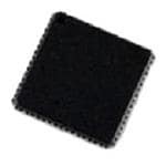
| 描述 | IC CLOCK GEN EXT VCO 64-LFCSP时钟发生器及支持产品 12 LVPECL/24 CMOS Output |
| DevelopmentKit | AD9520-5/PCBZ |
| 产品分类 | |
| 品牌 | Analog Devices |
| 产品手册 | |
| 产品图片 |
|
| rohs | 符合RoHS无铅 / 符合限制有害物质指令(RoHS)规范要求 |
| 产品系列 | 时钟和计时器IC,时钟发生器及支持产品,Analog Devices AD9520-5BCPZ- |
| 数据手册 | |
| 产品型号 | AD9520-5BCPZ |
| PLL | 是 |
| 产品目录页面 | |
| 产品种类 | 时钟发生器及支持产品 |
| 供应商器件封装 | 64-LFCSP-VQ(9x9) |
| 其它名称 | AD95205BCPZ |
| 分频器/倍频器 | 是/无 |
| 包装 | 托盘 |
| 商标 | Analog Devices |
| 安装类型 | 表面贴装 |
| 封装 | Tray |
| 封装/外壳 | 64-VFQFN 裸露焊盘,CSP |
| 封装/箱体 | LFCSP EP |
| 工作温度 | -40°C ~ 85°C |
| 工作电源电压 | 3.3 V |
| 工厂包装数量 | 260 |
| 差分-输入:输出 | 是/是 |
| 最大工作温度 | + 85 C |
| 最大输入频率 | 250 MHz |
| 最大输出频率 | 2400 MHz |
| 最小工作温度 | - 40 C |
| 标准包装 | 1 |
| 比率-输入:输出 | 2:12,2:24 |
| 电压-电源 | 3.135 V ~ 3.465 V |
| 电路数 | 1 |
| 类型 | Clock Generators |
| 系列 | AD9520-5 |
| 视频文件 | http://www.digikey.cn/classic/video.aspx?PlayerID=1364138032001&width=640&height=505&videoID=2585508883001 |
| 设计资源 | |
| 输入 | CMOS,LVDS,LVPECL |
| 输出 | CMOS,LVPECL |
| 输出端数量 | 12 |
| 输出类型 | LVPECL |
| 频率-最大值 | 2.4GHz |


- 商务部:美国ITC正式对集成电路等产品启动337调查
- 曝三星4nm工艺存在良率问题 高通将骁龙8 Gen1或转产台积电
- 太阳诱电将投资9.5亿元在常州建新厂生产MLCC 预计2023年完工
- 英特尔发布欧洲新工厂建设计划 深化IDM 2.0 战略
- 台积电先进制程称霸业界 有大客户加持明年业绩稳了
- 达到5530亿美元!SIA预计今年全球半导体销售额将创下新高
- 英特尔拟将自动驾驶子公司Mobileye上市 估值或超500亿美元
- 三星加码芯片和SET,合并消费电子和移动部门,撤换高东真等 CEO
- 三星电子宣布重大人事变动 还合并消费电子和移动部门
- 海关总署:前11个月进口集成电路产品价值2.52万亿元 增长14.8%


PDF Datasheet 数据手册内容提取
12 LVPECL/24 CMOS Output Clock Generator Data Sheet AD9520-5 FEATURES FUNCTIONAL BLOCK DIAGRAM Low phase noise, phase-locked loop (PLL) CP Optional external 3.3 V/5 V VCO/VCXO to 2.4 GHz 1 differential or 2 single-ended reference inputs REF1 RR STATUS Accepts CMOS, LVDS, or LVPECL references to 250 MHz VETO MONITOR AOcpcteiopntsa 1l r6e.6fe2r eMnHcez tcolo 3c3k. d3 oMuHbzle crr ystal for reference input RREEFFIINN REF2 WITCHOND MONI PLL SA Reference monitoring capability ZERO Automatic/ manual reference holdover and reference CLK DIVIDER DELAY switchover modes, with revertive switching CLK AND MUXES Glitch-free switchover between references LVPECL/ CMOS OUT0 Automatic recovery from holdover DIV/Φ OUT1 Digital or analog lock detect, selectable OUT2 Optional zero delay operation OUT3 DIV/Φ OUT4 Twelve 1.6 GHz LVPECL outputs divided into 4 groups OUT5 Each group of 3 outputs shares a 1-to-32 divider with OUT6 DIV/Φ OUT7 phase delay OUT8 Additive output jitter as low as 225 fs rms OUT9 DIV/Φ OUT10 Channel-to-channel skew grouped outputs < 16 ps OUT11 Each LVPECL output can be configured as 2 CMOS outputs (for f ≤ 250 MHz) SPI/I2C CONTROL AMuatnoumaal toiucO UtspTyuntc shyrnonchizraotnioizna toifo anl la ovuaitlpaubtlse on power-up DIGPOITRATL ALNODGIC EEPROM AD9520-5 07239-001 Figure 1. SPI- and I²C-compatible serial control port 64-lead LFCSP Nonvolatile EEPROM stores configuration settings APPLICATIONS Low jitter, low phase noise clock distribution Clock generation and translation for SONET, 10Ge, 10GFC, Synchronous Ethernet, OTU2/3/4 Forward error correction (G.710) The AD9520-5 features 12 LVPECL outputs in four groups. Any Clocking high speed ADCs, DACs, DDSs, DDCs, DUCs, MxFEs of the 1.6 GHz LVPECL outputs can be reconfigured as two High performance wireless transceivers 250 MHz CMOS outputs. If an application requires LVDS ATE and high performance instrumentation drivers instead of LVPECL drivers, refer to the AD9522-5. Broadband infrastructures Each group of three outputs has a divider that allows both the GENERAL DESCRIPTION divide ratio (from 1 to 32) and the phase offset or coarse time delay to be set. The AD9520-51 provides a multioutput clock distribution function with subpicosecond jitter performance, along with The AD9520-5 is available in a 64-lead LFCSP and can be operated an on-chip PLL that can be used with an external VCO. from a single 3.3 V supply. The external VCO can have an operating voltage of up to 5.5 V. A separate output driver power The AD9520-5 serial interface supports both SPI and I²C ports. supply can be from 2.375 V to 3.465 V. An in-package EEPROM, which can be programmed through the serial interface, can store user-defined register settings for The AD9520-5 is specified for operation over the standard power-up and chip reset. industrial range of −40°C to +85°C. 1 AD9520 is used throughout this data sheet to refer to all the members of the AD9520 family. However, when AD9520-5 is used, it refers to that specific member of the AD9520 family. Rev. B Document Feedback Information furnished by Analog Devices is believed to be accurate and reliable. However, no responsibility is assumed by Analog Devices for its use, nor for any infringements of patents or other One Technology Way, P.O. Box 9106, Norwood, MA 02062-9106, U.S.A. rights of third parties that may result from its use. Specifications subject to change without notice. No license is granted by implication or otherwise under any patent or patent rights of Analog Devices. Tel: 781.329.4700 ©2008–2016 Analog Devices, Inc. All rights reserved. Trademarks and registered trademarks are the property of their respective owners. Technical Support www.analog.com
AD9520-5 Data Sheet TABLE OF CONTENTS Features .............................................................................................. 1 Detailed Block Diagram ................................................................ 25 Applications ....................................................................................... 1 Theory of Operation ...................................................................... 26 General Description ......................................................................... 1 Operational Configurations ...................................................... 26 Functional Block Diagram .............................................................. 1 Zero Delay Operation ................................................................ 37 Revision History ............................................................................... 3 Clock Distribution ..................................................................... 38 Specifications ..................................................................................... 4 Reset Modes ................................................................................ 43 Power Supply Requirements ....................................................... 4 Power-Down Modes .................................................................. 44 PLL Characteristics ...................................................................... 4 Serial Control Port ......................................................................... 45 Clock Inputs .................................................................................. 7 SPI/I²C Port Selection ................................................................ 45 Clock Outputs ............................................................................... 7 I²C Serial Port Operation .......................................................... 45 Timing Characteristics ................................................................ 8 SPI Serial Port Operation .......................................................... 48 Clock Output Additive Phase Noise (Distribution Only; VCO SPI Instruction Word (16 Bits) ................................................. 49 Divider Not Used) ...................................................................... 10 SPI MSB/LSB First Transfers .................................................... 49 Clock Output Absolute Time Jitter (Clock Generation Using EEPROM Operations ..................................................................... 52 External VCXO) ......................................................................... 11 Writing to the EEPROM ........................................................... 52 Clock Output Additive Time Jitter (VCO Divider Not Used) ....................................................................................................... 11 Reading from the EEPROM ..................................................... 52 Clock Output Additive Time Jitter (VCO Divider Used) ..... 12 Programming the EEPROM Buffer Segment ......................... 53 Serial Control Port—SPI Mode ................................................ 12 Thermal Performance .................................................................... 54 Serial Control Port—I²C Mode ................................................ 13 Register Map ................................................................................... 55 Register Map Descriptions ............................................................ 58 PD, SYNC, EEPROM, and RESET Pins .................................. 14 Applications Information .............................................................. 71 Serial Port Setup Pins—SP1, SP0 ............................................. 14 Frequency Planning Using the AD9520 .................................. 71 LD, STATUS, and REFMON Pins ............................................ 14 Using the AD9520 Outputs for ADC Clock Applications .... 71 Power Dissipation ....................................................................... 15 LVPECL Clock Distribution ..................................................... 72 Absolute Maximum Ratings .......................................................... 16 CMOS Clock Distribution ........................................................ 72 Thermal Resistance .................................................................... 16 Outline Dimensions ....................................................................... 74 ESD Caution ................................................................................ 16 Ordering Guide .......................................................................... 74 Pin Configuration and Function Descriptions ........................... 17 Typical Performance Characteristics ........................................... 20 Terminology .................................................................................... 24 Rev. B | Page 2 of 74
Data Sheet AD9520-5 REVISION HISTORY 10/2016—Rev. A to Rev. B Change to LVPECL Output Drivers Section; Changes to CMOS Changed AD9520 to AD9520-5 .................................. Throughout Output Drivers Section and Power-On Reset Section ............... 43 Change to PD Power-Down, Maximum Sleep Parameter, Changes to Soft Reset via the Serial Port Section and Soft Table 15 .............................................................................................1 5 Reset to Settings in EEPROM when EEPROM Pin = 0b Updated Outline Dimensions ........................................................ 74 via the Serial Port Section .............................................................. 44 Change to Pin Descriptions Section and SPI Mode Operation 8/2013—Rev. 0 to Rev. A Section .............................................................................................. 48 Changes to Features Section, Applications Section, and Changes to SPI Instruction Word (16 Bits) Section ................... 49 General Description Section ............................................................ 1 Changes to EEPROM Operations Section, Writing to the Changes to Table 2 ............................................................................ 4 EEPROM Section, and Reading from the EEPROM Section ... 52 Changes to Input Frequency Parameter; Change to Input Changes to Register Section Definition Group Section; Sensitivity, Differential Parameter Test Conditions/Comments, Added Operational Codes Section Heading ............................... 53 Table 3 ................................................................................................. 7 Changes to Table 44 ........................................................................ 55 Change to Output Differential Voltage, V Parameter Test Added Unused Bits to Register Map Descriptions Section; OD Conditions/Comments; Added Source Current and Sink Changes to Address 0x000, Bit 5, and Added Address 0x003, Current Parameters, Table 4 ............................................................ 7 Table 45; Changes to Address 0x000, Bit 5, and Added Reordered Figure 2 to Figure 4 ........................................................ 9 Address 0x003, Table 46 ................................................................. 58 Change to Reset Timing, Pulse Width Low Parameter, Table 12 ... 14 Changes to Address 0x017, Bits[7:2], Table 48............................ 60 Change to Junction Temperature, Table 16; Reformatted Changes to Address 0x018, Bit 4, Table 48 .................................. 61 Table 16 ........................................................................................................ 16 Changes to Address 0x01A, Bits[5:0], Setting 101010, Added NC Note to Figure 5; Change to Pin 4 and Pin 22 Table 48 ............................................................................................. 62 Description, Table 18 ...................................................................... 17 Changes to Address 0x01B, Bits[4:0], Table 48 ........................... 63 Reordered Figure 21 and Figure 22 .............................................. 22 Changes to Address 0x191, Bit 5, and Address 0x194, Bit 5, Added Figure 25, Renumbered Sequentially ............................... 23 Table 50 ............................................................................................. 66 Change to Configuration of the PLL Section and Changes Changes to Address 0x197, Bit 5, Table 50 .................................. 67 to Charge Pump (CP) Section ....................................................... 30 Changes to Address 0x19A, Bit 5, Table 50 ................................. 68 Change to PLL Reference Inputs Section; Changes to Changes to Table 54 ........................................................................ 69 Reference Switchover Section ........................................................ 31 Changes to Address 0xB02, Bit 0, and Address 0xB03, Bit 0, Change to Prescaler Section and A and B Counters Section .... 32 Table 55 ............................................................................................. 70 Changes to Table 25 ........................................................................ 33 Change to Frequency Planning Using the AD9520 Section ..... 71 Change to Clock Frequency Division Section; Changes to Added LVPECL Y-Termination and Far-End Thevenin VCO Divider Section; Added Channel Divider Maximum Termination Headings; Changes to CMOS Clock Distribution Frequency Section ........................................................................... 39 Section .............................................................................................. 72 Reformatted Table 30 to Table 33 .................................................. 40 Change to Phase Offset or Coarse Time Delay Section ............. 41 10/2008—Revision 0: Initial Version Rev. B | Page 3 of 74
AD9520-5 Data Sheet SPECIFICATIONS Typical is given for V = V = 3.3 V ± 5%; V ≤ V ≤ 5.25 V; T = 25°C; R = 4.12 kΩ; CP = 5.1 kΩ, unless otherwise noted. Minimum S S_DRV S CP A SET RSET and maximum values are given over full V and T (−40°C to +85°C) variation. S A POWER SUPPLY REQUIREMENTS Table 1. Parameter Min Typ Max Unit Test Conditions/Comments POWER PINS VS 3.135 3.3 3.465 V 3.3 V ± 5% VS_DRV 2.375 V V Nominally 2.5 V to 3.3 V ± 5% S VCP V 5.25 V Nominally 3.3 V to 5.0 V ± 5% S CURRENT SET RESISTORS RSET Pin Resistor 4.12 kΩ Sets internal biasing currents; connect to ground CPRSET Pin Resistor 5.1 kΩ Sets internal CP current range, nominally 4.8 mA (CP_lsb = 600 µA); actual current can be calculated by CP_lsb = 3.06/CP ; connect to ground RSET PLL CHARACTERISTICS Table 2. Parameter Min Typ Max Unit Test Conditions/Comments REFERENCE INPUTS Differential Mode (REFIN, REFIN) Differential mode (can accommodate single-ended input by ac grounding undriven input) Input Frequency 0 250 MHz Frequencies below about 1 MHz should be dc- coupled; be careful to match V (self-bias voltage) CM Input Sensitivity 280 mV p- PLL figure of merit (FOM) increases with increasing p slew rate (see Figure 11); the input sensitivity is sufficient for ac-coupled LVDS and LVPECL signals Self-Bias Voltage, REFIN 1.35 1.60 1.75 V Self-bias voltage of REFIN1 Self-Bias Voltage, REFIN 1.30 1.50 1.60 V Self-bias voltage of REFIN1 Input Resistance, REFIN 4.0 4.8 5.9 kΩ Self-biased1 Input Resistance, REFIN 4.4 5.3 6.4 kΩ Self-biased1 Dual Single-Ended Mode (REF1, REF2) Two single-ended CMOS-compatible inputs Input Frequency (AC-Coupled with 10 250 MHz Slew rate must be >50 V/µs DC Offset Off) Input Frequency (AC-Coupled with 250 MHz Slew rate must be >50 V/µs, and input amplitude DC Offset On) sensitivity specification must be met; see the input sensitivity parameter Input Frequency (DC-Coupled) 0 250 MHz Slew rate > 50 V/µs; CMOS levels Input Sensitivity (AC-Coupled 0.55 3.28 V p-p V should not exceed V IH S with DC Offset Off) Input Sensitivity (AC-Coupled with 1.5 2.78 V p-p V should not exceed V IH S DC Offset On) Input Logic High, DC Offset Off 2.0 V Input Logic Low, DC Offset Off 0.8 V Input Current −100 +100 µA Input Capacitance 2 pF Each pin, REFIN (REF1)/REFIN (REF2) Pulse Width High/Low 1.8 ns The amount of time that a square wave is high/low; determines the allowable input duty cycle Crystal Oscillator Crystal Resonator Frequency Range 16.62 33.33 MHz Maximum Crystal Motional Resistance 30 Ω Rev. B | Page 4 of 74
Data Sheet AD9520-5 Parameter Min Typ Max Unit Test Conditions/Comments PHASE/FREQUENCY DETECTOR (PFD) PFD Input Frequency 100 MHz Antibacklash pulse width = 1.3 ns 45 MHz Antibacklash pulse width = 2.9 ns Reference Input Clock Doubler Frequency 0.004 50 MHz Antibacklash Pulse Width 1.3 ns Register 0x017[1:0] = 01b 2.9 ns Register 0x017[1:0] = 00b; Register 0x017[1:0] = 11b 6.0 ns Register 0x017[1:0] = 10b CHARGE PUMP (CP) CP is the CP pin voltage; V is the charge pump V CP power supply voltage (VCP pin) I Sink/Source Programmable CP High Value 4.8 mA With CP = 5.1 kΩ; higher I is possible by RSET CP changing CP RSET Low Value 0.60 mA With CP = 5.1 kΩ; lower I is possible by RSET CP changing CP RSET Absolute Accuracy 2.5 % CP = V /2 V CP CP Range 2.7 10 kΩ RSET I High Impedance Mode Leakage 1 nA CP Sink-and-Source Current Matching 1 % 0.5 V < CP < V − 0.5 V; CP is the CP pin voltage; V CP V V is the charge pump power supply voltage CP (VCP pin) I vs. V 1.5 % 0.5 V < CP < V − 0.5 V CP CP V CP I vs. Temperature 2 % CP = V /2 CP V CP PRESCALER (PART OF N DIVIDER) Prescaler Input Frequency P = 1 FD 300 MHz P = 2 FD 600 MHz P = 3 FD 900 MHz P = 2 DM (2/3) 200 MHz P = 4 DM (4/5) 1000 MHz P = 8 DM (8/9) 2400 MHz P = 16 DM (16/17) 3000 MHz P = 32 DM (32/33) 3000 MHz Prescaler Output Frequency 300 MHz A, B counter input frequency (prescaler input frequency divided by P) PLL N DIVIDER DELAY Register 0x019[2:0]; see Table 48 000 Off 001 385 ps 010 486 ps 011 623 ps 100 730 ps 101 852 ps 110 976 ps 111 1101 ps PLL R DIVIDER DELAY Register 0x019[5:3]; see Table 48 000 Off 001 365 ps 010 486 ps 011 608 ps 100 730 ps 101 852 ps 110 976 ps 111 1101 ps Rev. B | Page 5 of 74
AD9520-5 Data Sheet Parameter Min Typ Max Unit Test Conditions/Comments PHASE OFFSET IN ZERO DELAY REF refers to REFIN (REF1)/REFIN (REF2) Phase Offset (REF-to-LVPECL Clock Output 560 1060 1310 ps When N delay and R delay are bypassed Pins) in Zero Delay Mode Phase Offset (REF-to-LVPECL Clock Output −320 +50 +240 ps When N delay setting = 110b, and R delay is bypassed Pins) in Zero Delay Mode NOISE CHARACTERISTICS In-Band Phase Noise of the Charge Pump/ The PLL in-band phase noise floor is estimated by Phase Frequency Detector2 measuring the in-band phase noise at the output of the VCO and subtracting 20 log(N) (where N is the value of the N divider) 500 kHz PFD Frequency −165 dBc/Hz 1 MHz PFD Frequency −162 dBc/Hz 10 MHz PFD Frequency −152 dBc/Hz 50 MHz PFD Frequency −144 dBc/Hz PLL Figure of Merit (FOM) −222 dBc/Hz Reference slew rate > 0.5 V/ns; FOM + 10 log(f ) is PFD an approximation of the PFD/CP in-band phase noise (in the flat region) inside the PLL loop bandwidth; when running closed-loop, the phase noise, as observed at the VCO output, is increased by 20 log(N); PLL figure of merit decreases with decreasing slew rate; see Figure 11 PLL DIGITAL LOCK DETECT WINDOW3 Signal available at the LD, STATUS, and REFMON pins when selected by appropriate register settings; the lock detect threshold varies linearly with the value of the CP resistor RSET Lock Threshold (Coincidence of Edges) Selected by Register 0x017[1:0] and Register 0x018[4] (this is the threshold to go from unlock to lock) Low Range (ABP 1.3 ns, 2.9 ns) 3.5 ns Register 0x017[1:0] = 00b, 01b,11b; Register 0x018[4] = 1b High Range (ABP 1.3 ns, 2.9 ns) 7.5 ns Register 0x017[1:0] = 00b, 01b, 11b; Register 0x018[4] = 0b High Range (ABP 6.0 ns) 3.5 ns Register 0x017[1:0] = 10b; Register 0x018[4] = 0b Unlock Threshold (Hysteresis)3 Selected by Register 0x017[1:0] and Register 0x018[4] (this is the threshold to go from lock to unlock) Low Range (ABP 1.3 ns, 2.9 ns) 7 ns Register 0x017[1:0] = 00b, 01b, 11b; Register 0x018[4] = 1b High Range (ABP 1.3 ns, 2.9 ns) 15 ns Register 0x017[1:0] = 00b, 01b, 11b; Register 0x018[4] = 0b High Range (ABP 6.0 ns) 11 ns Register 0x017[1:0] = 10b; Register 0x018[4] = 0b 1 The REFIN and REFIN self-bias points are offset slightly to avoid chatter on an open input condition. 2 In-band means within the LBW of the PLL. 3 For reliable operation of the digital lock detect, the period of the PFD frequency must be greater than the unlock-after-lock time. Rev. B | Page 6 of 74
Data Sheet AD9520-5 CLOCK INPUTS Table 3. Parameter Min Typ Max Unit Test Conditions/Comments CLOCK INPUTS (CLK, CLK) Differential input Input Frequency 01 2.4 GHz High frequency distribution (VCO divider) 01 2.0 GHz Distribution only (VCO divider bypassed); this is the frequency range supported by the channel divider for all divide ratios except divide-by-17 and divide-by-3 01 1.6 GHz Distribution only (VCO divider bypassed); this is the frequency range supported by all channel divider ratios Input Sensitivity, Differential 150 mV p-p Measured at 2.4 GHz; jitter performance is improved with slew rates > 1 V/ns ; the input sensitivity is sufficient for ac-coupled LVDS and LVPECL signals Input Level, Differential 2 V p-p Larger voltage swings can turn on the protection diodes and can degrade jitter performance Input Common-Mode Voltage, V 1.3 1.57 1.8 V Self-biased; enables ac coupling CM Input Common-Mode Range, V 1.3 1.8 V With 200 mV p-p signal applied; dc-coupled CMR Input Sensitivity, Single-Ended 150 mV p-p CLK ac-coupled; CLK ac-bypassed to RF ground Input Resistance 3.9 4.7 5.7 kΩ Self-biased Input Capacitance 2 pF 1 Below about 1 MHz, the input should be dc-coupled. Care should be taken to match VCM. CLOCK OUTPUTS Table 4. Parameter Min Typ Max Unit Test Conditions/Comments LVPECL CLOCK OUTPUTS Termination = 50 Ω to V − 2 V S_DRV OUT0, OUT1, OUT2, OUT3, OUT4, OUT5, Differential (OUT, OUT) OUT6, OUT7, OUT8, OUT9, OUT10, OUT11 Output Frequency, Maximum 2400 MHz Using direct to output (see Figure 17); higher frequencies are possible, but the resulting amplitude does not meet the V specification; the maximum output frequency is limited OD by the maximum frequency at the CLK inputs Output High Voltage, V V − V V V OH S_DRV S_DRV S_DRV 1.07 − 0.96 − 0.84 Output Low Voltage, V V − V V V OL S_DRV S_DRV S_DRV 1.95 − 1.79 − 1.64 Output Differential Voltage, V 660 820 950 mV V − V for each leg of a differential pair for default OD OH OL amplitude setting with the driver not toggling; the peak-to- peak amplitude measured using a differential probe across the differential pair with the driver toggling is roughly 2× these values (see Figure 17 for variation over frequency) CMOS CLOCK OUTPUTS OUT0A, OUT0B, OUT1A, OUT1B, OUT2A, Single-ended; termination = 10 pF OUT2B, OUT3A, OUT3B, OUT4A, OUT4B, OUT5A, OUT5B, OUT6A, OUT6B, OUT7A, OUT7B, OUT8A, OUT8B, OUT9A, OUT9B, OUT10A, OUT10B, OUT11A, OUT11B Output Frequency 250 MHz See Figure 18 Output Voltage High, V V − V 1 mA load, V = 3.3 V/2.5 V OH S S_DRV 0.1 Output Voltage Low, V 0.1 V 1 mA load, V = 3.3 V/2.5 V OL S_DRV Output Voltage High, V 2.7 V 10 mA load, V = 3.3 V OH S_DRV Output Voltage Low, V 0.5 V 10 mA load, V = 3.3 V OL S_DRV Output Voltage High, V 1.8 V 10 mA load, V = 2.5 V OH S_DRV Output Voltage Low, V 0.6 V 10 mA load, V = 2.5 V OL S_DRV Rev. B | Page 7 of 74
AD9520-5 Data Sheet Parameter Min Typ Max Unit Test Conditions/Comments Source Current Damage to the part can result if values are exceeded Static 20 mA Dynamic 16 mA Sink Current Damage to the part can result if values are exceeded Static 8 mA Dynamic 16 mA TIMING CHARACTERISTICS Table 5. Parameter Min Typ Max Unit Test Conditions/Comments LVPECL OUTPUT RISE/FALL TIMES Termination = 50 Ω to V − 2 V S_DRV Output Rise Time, t 130 170 ps 20% to 80%, measured differentially (rise/fall times are RP independent of V and are valid for V = 3.3 V and 2.5 V) S S_DRV Output Fall Time, t 130 170 ps 80% to 20%, measured differentially (rise/fall times are FP independent of V and are valid for V = 3.3 V and 2.5 V) S S_DRV PROPAGATION DELAY, t , CLK-TO-LVPECL PECL OUTPUT For All Divide Values 850 1050 1280 ps High frequency clock distribution configuration 800 970 1180 ps Clock distribution configuration Variation with Temperature 1.0 ps/°C OUTPUT SKEW, LVPECL OUTPUTS1 Termination = 50 Ω to V − 2 V S_DRV LVPECL Outputs Sharing the Same Divider 5 16 ps V = 3.3 V S_DRV 5 20 ps V = 2.5 V S_DRV LVPECL Outputs on Different Dividers 5 45 ps V = 3.3 V S_DRV 5 60 ps V = 2.5 V S_DRV All LVPECL Outputs Across Multiple Parts 190 ps V = 3.3 V and 2.5 V S_DRV CMOS OUTPUT RISE/FALL TIMES Termination = open Output Rise Time, t 750 960 ps 20% to 80%; C = 10 pF; V = 3.3 V RC LOAD S_DRV Output Fall Time, t 715 890 ps 80% to 20%; C = 10 pF; V = 3.3 V FC LOAD S_DRV Output Rise Time, t 965 1280 ps 20% to 80%; C = 10 pF; V = 2.5 V RC LOAD S_DRV Output Fall Time, t 890 1100 ps 80% to 20%; C = 10 pF; V = 2.5 V FC LOAD S_DRV PROPAGATION DELAY, t , CLK-TO-CMOS Clock distribution configuration CMOS OUTPUT For All Divide Values 2.1 2.75 3.55 ns V = 3.3 V S_DRV 3.35 ns V = 2.5 V S_DRV Variation with Temperature 2 ps/°C V = 3.3 V and 2.5 V S_DRV OUTPUT SKEW, CMOS OUTPUTS1 CMOS Outputs Sharing the Same Divider 7 85 ps V = 3.3 V S_DRV 10 105 ps V = 2.5 V S_DRV All CMOS Outputs on Different Dividers 10 240 ps V = 3.3 V S_DRV 10 285 ps V = 2.5 V S_DRV All CMOS Outputs Across Multiple Parts 600 ps V = 3.3 V S_DRV 620 ps V = 2.5 V S_DRV OUTPUT SKEW, LVPECL-TO-CMOS OUTPUTS1 All settings identical; different logic type Outputs Sharing the Same Divider 1.18 1.76 2.48 ns LVPECL to CMOS on same part Outputs on Different Dividers 1.20 1.78 2.50 ns LVPECL to CMOS on same part 1 The output skew is the difference between any two similar delay paths while operating at the same voltage and temperature. Rev. B | Page 8 of 74
Data Sheet AD9520-5 Timing Diagrams DIFFERENTIAL SINGLE-ENDED 80% 80% LVPECL CMOS 10pF LOAD 20% 20% tRP tFP 07239-061 tRC tFC 07239-063 Figure 2. LVPECL Timing, Differential Figure 4. CMOS Timing, Single-Ended, 10 pF Load t CLK CLK t PECL tCMOS 07239-060 Figure 3. CLK/CLK to Clock Output Timing, DIV = 1 Rev. B | Page 9 of 74
AD9520-5 Data Sheet CLOCK OUTPUT ADDITIVE PHASE NOISE (DISTRIBUTION ONLY; VCO DIVIDER NOT USED) Table 6. Parameter Min Typ Max Unit Test Conditions/Comments CLK-TO-LVPECL ADDITIVE PHASE NOISE Distribution section only; does not include the PLL CLK = 1 GHz, Output = 1 GHz Input slew rate > 1 V/ns Divider = 1 10 Hz Offset −107 dBc/Hz 100 Hz Offset −117 dBc/Hz 1 kHz Offset −127 dBc/Hz 10 kHz Offset −135 dBc/Hz 100 kHz Offset −142 dBc/Hz 1 MHz Offset −145 dBc/Hz 10 MHz Offset −147 dBc/Hz 100 MHz Offset −150 dBc/Hz CLK = 1 GHz, Output = 200 MHz Input slew rate > 1 V/ns Divider = 5 10 Hz Offset −122 dBc/Hz 100 Hz Offset −132 dBc/Hz 1 kHz Offset −143 dBc/Hz 10 kHz Offset −150 dBc/Hz 100 kHz Offset −156 dBc/Hz 1 MHz Offset −157 dBc/Hz >10 MHz Offset −157 dBc/Hz CLK-TO-CMOS ADDITIVE PHASE NOISE Distribution section only; does not include the PLL CLK = 1 GHz, Output = 250 MHz Input slew rate > 1 V/ns Divider = 4 10 Hz Offset −107 dBc/Hz 100 Hz Offset −119 dBc/Hz 1 kHz Offset −125 dBc/Hz 10 kHz Offset −134 dBc/Hz 100 kHz Offset −144 dBc/Hz 1 MHz Offset −148 dBc/Hz >10 MHz Offset −154 dBc/Hz CLK = 1 GHz, Output = 50 MHz Input slew rate > 1 V/ns Divider = 20 10 Hz Offset −126 dBc/Hz 100 Hz Offset −133 dBc/Hz 1 kHz Offset −140 dBc/Hz 10 kHz Offset −148 dBc/Hz 100 kHz Offset −157 dBc/Hz 1 MHz Offset −160 dBc/Hz >10 MHz Offset −163 dBc/Hz Rev. B | Page 10 of 74
Data Sheet AD9520-5 CLOCK OUTPUT ABSOLUTE TIME JITTER (CLOCK GENERATION USING EXTERNAL VCXO) Table 7. Parameter Min Typ Max Unit Test Conditions/Comments LVPECL OUTPUT ABSOLUTE TIME JITTER Application example based on a typical setup using an external 245.76 MHz VCXO (Toyocom TCO-2112); reference = 15.36 MHz; R DIV = 1 LVPECL = 245.76 MHz; PLL LBW = 125 Hz 54 fs rms Integration BW = 200 kHz to 5 MHz 77 fs rms Integration BW = 200 kHz to 10 MHz 109 fs rms Integration BW = 12 kHz to 20 MHz LVPECL = 122.88 MHz; PLL LBW = 125 Hz 79 fs rms Integration BW = 200 kHz to 5 MHz 114 fs rms Integration BW = 200 kHz to 10 MHz 163 fs rms Integration BW = 12 kHz to 20 MHz LVPECL = 61.44 MHz; PLL LBW = 125 Hz 124 fs rms Integration BW = 200 kHz to 5 MHz 176 fs rms Integration BW = 200 kHz to 10 MHz 259 fs rms Integration BW = 12 kHz to 20 MHz CLOCK OUTPUT ADDITIVE TIME JITTER (VCO DIVIDER NOT USED) Table 8. Parameter Min Typ Max Unit Test Conditions/Comments LVPECL OUTPUT ADDITIVE TIME JITTER Distribution section only; does not include the PLL; measured at rising edge of the clock signal CLK = 622.08 MHz 46 fs rms Integration bandwidth = 12 kHz to 20 MHz Any LVPECL Output = 622.08 MHz Divide Ratio = 1 CLK = 622.08 MHz 64 fs rms Integration bandwidth = 12 kHz to 20 MHz Any LVPECL Output = 155.52 MHz Divide Ratio = 4 CLK = 1000 MHz 223 fs rms Calculated from SNR of ADC method Any LVPECL Output = 100 MHz Broadband jitter Divide Ratio = 10 CLK = 500 MHz 209 fs rms Calculated from SNR of ADC method Any LVPECL Output = 100 MHz Broadband jitter Divide Ratio = 5 CMOS OUTPUT ADDITIVE TIME JITTER Distribution section only; does not include the PLL CLK = 200 MHz 325 fs rms Calculated from SNR of ADC method Any CMOS Output Pair = 100 MHz Broadband jitter Divide Ratio = 2 Rev. B | Page 11 of 74
AD9520-5 Data Sheet CLOCK OUTPUT ADDITIVE TIME JITTER (VCO DIVIDER USED) Table 9. Parameter Min Typ Max Unit Test Conditions/Comments LVPECL OUTPUT ADDITIVE TIME JITTER Distribution section only; does not include PLL; uses rising edge of clock signal CLK = 1.0 GHz; VCO DIV = 5; LVPECL = 100 MHz; 230 fs rms Calculated from SNR of ADC method Channel Divider = 2; Duty-Cycle Correction = Off (broadband jitter) CLK = 500 MHz; VCO DIV = 5; LVPECL = 100 MHz; 215 fs rms Calculated from SNR of ADC method Bypass Channel Divider; Duty-Cycle Correction = On (broadband jitter) CMOS OUTPUT ADDITIVE TIME JITTER Distribution section only; does not include PLL; uses rising edge of clock signal CLK = 200 MHz; VCO DIV = 2; CMOS = 100 MHz; 326 fs rms Calculated from SNR of ADC method Bypass Channel Divider; Duty-Cycle Correction = Off (broadband jitter) CLK = 1600 MHz; VCO DIV = 2; CMOS = 100 MHz; 362 fs rms Calculated from SNR of ADC method Channel Divider = 8; Duty-Cycle Correction = Off (broadband jitter) SERIAL CONTROL PORT—SPI MODE Table 10. Parameter Min Typ Max Unit Test Conditions/Comments CS (INPUT) CS has an internal 30 kΩ pull-up resistor Input Logic 1 Voltage 2.0 V Input Logic 0 Voltage 0.8 V Input Logic 1 Current 3 µA Input Logic 0 Current −110 µA The minus sign indicates that current is flowing out of the AD9520-5, which is due to the internal pull-up resistor Input Capacitance 2 pF SCLK (INPUT) IN SPI MODE SCLK has an internal 30 kΩ pull-down resistor in SPI mode, but not in I2C mode Input Logic 1 Voltage 2.0 V Input Logic 0 Voltage 0.8 V Input Logic 1 Current 110 µA Input Logic 0 Current 1 µA Input Capacitance 2 pF SDIO (INPUT IN BIDIRECTIONAL MODE) Input Logic 1 Voltage 2.0 V Input Logic 0 Voltage 0.8 V Input Logic 1 Current 1 µA Input Logic 0 Current 1 µA Input Capacitance 2 pF SDIO, SDO (OUTPUTS) Output Logic 1 Voltage 2.7 V Output Logic 0 Voltage 0.4 V TIMING Clock Rate (SCLK, 1/t ) 25 MHz SCLK Pulse Width High, t 16 ns HIGH Pulse Width Low, t 16 ns LOW SDIO to SCLK Setup, t 4 ns DS SCLK to SDIO Hold, t 0 ns DH SCLK to Valid SDIO and SDO, t 11 ns DV CS to SCLK Setup and Hold, tS, tC 2 ns CS Minimum Pulse Width High, tPWH 3 ns Rev. B | Page 12 of 74
Data Sheet AD9520-5 SERIAL CONTROL PORT—I²C MODE Table 11. Parameter Min Typ Max Unit Test Conditions/Comments SDA, SCL (WHEN INPUTTING DATA) Input Logic 1 Voltage 0.7 × V V S Input Logic 0 Voltage 0.3 × V V S Input Current with an Input Voltage Between 0.1 × V −10 +10 µA S and 0.9 × V S Hysteresis of Schmitt Trigger Inputs 0.015 × V V S Pulse Width of Spikes That Must Be Suppressed by the 50 ns Input Filter, t SPIKE SDA (WHEN OUTPUTTING DATA) Output Logic 0 Voltage at 3 mA Sink Current 0.4 V Output Fall Time from VIH to VIL with a Bus 20 + 0.1 C 250 ns C = capacitance of one bus line in pF MIN MAX b b Capacitance from 10 pF to 400 pF TIMING Note that all I2C timing values are referred to VIH (0.3 × V) and MIN S VIL levels (0.7 × V) MAX S Clock Rate (SCL, f ) 400 kHz I2C Bus Free Time Between a Stop and Start Condition, t 1.3 µs IDLE Setup Time for a Repeated Start Condition, t 0.6 µs SET; STR Hold Time (Repeated) Start Condition, t 0.6 µs After this period, the first clock pulse HLD; STR is generated Setup Time for Stop Condition, t 0.6 µs SET; STP Low Period of the SCL Clock, t 1.3 µs LOW High Period of the SCL Clock, t 0.6 µs HIGH SCL, SDA Rise Time, t 20 + 0.1 C 300 ns RISE b SCL, SDA Fall Time, t 20 + 0.1 C 300 ns FALL b Data Setup Time, t 120 ns This is a minor deviation from the SET; DAT original I²C specification of 100 ns minimum Data Hold Time, t 140 880 ns This is a minor deviation from the HLD; DAT original I²C specification of 0 ns minimum1 Capacitive Load for Each Bus Line, C 400 pF b 1 According to the original I2C specification, an I2C master must also provide a minimum hold time of 300 ns for the SDA signal to bridge the undefined region of the SCL falling edge. Rev. B | Page 13 of 74
AD9520-5 Data Sheet PD, SYNC, EEPROM, AND RESET PINS Table 12. Parameter Min Typ Max Unit Test Conditions/Comments INPUT CHARACTERISTICS Each pin has a 30 kΩ internal pull-up resistor Logic 1 Voltage 2.0 V Logic 0 Voltage 0.8 V Logic 1 Current 1 µA Logic 0 Current −110 µA The minus sign indicates that current is flowing out of the AD9520-5, which is due to the internal pull-up resistor Capacitance 2 pF RESET TIMING Pulse Width Low 500 ns RESET Inactive to Start of Register 100 ns Programming SYNC TIMING Pulse Width Low 1.3 ns High speed clock is CLK input signal SERIAL PORT SETUP PINS—SP1, SP0 Table 13. Parameter Min Typ Max Unit Test Conditions/Comments SP1, SP0 These pins do not have internal pull-up/pull-down resistors Logic Level 0 0.25 × V V V is the voltage on the VS pin S S Logic Level ½ 0.4 × V 0.65 × V V These pins can be floated to obtain Logic Level ½; if S S floating the pin, connect a capacitor to ground Logic Level 1 0.8 × V V S LD, STATUS, AND REFMON PINS Table 14. Parameter Min Typ Max Unit Test Conditions/Comments OUTPUT CHARACTERISTICS When selected as a digital output (CMOS); there are other modes in which these pins are not CMOS digital outputs; see Table 48, Register 0x017, Register 0x01A, and Register 0x01B Output Voltage High, V 2.7 V OH Output Voltage Low, V 0.4 V OL MAXIMUM TOGGLE RATE 100 MHz Applies when mux is set to any divider or counter output or PFD up/down pulse; also applies in analog lock detect mode; usually debug mode only; beware that spurs can couple to output when any pin is toggling ANALOG LOCK DETECT Capacitance 3 pF On-chip capacitance; used to calculate RC time constant for analog lock detect readback; use a pull-up resistor REF1, REF2, AND CLK FREQUENCY STATUS MONITOR Normal Range 1.02 MHz Frequency above which the monitor indicates the presence of the reference Extended Range 8 kHz Frequency above which the monitor indicates the presence of the reference LD PIN COMPARATOR Trip Point 1.6 V Hysteresis 260 mV Rev. B | Page 14 of 74
Data Sheet AD9520-5 POWER DISSIPATION Table 15. Parameter Min Typ Max Unit Test Conditions/Comments POWER DISSIPATION, CHIP Does not include power dissipated in external resistors; all LVPECL outputs terminated with 50 Ω to V − 2 V; all CMOS CC outputs have 10 pF capacitive loading; V = 3.3 V S_DRV Power-On Default 1.32 1.5 W No clock; no programming; default register values Distribution Only Mode; VCO Divider On; 0.39 0.46 W f = 2.4 GHz; f = 200 MHz; VCO divider = 2; one LVPECL CLK OUT One LVPECL Output Enabled output and output divider enabled; zero delay off Distribution Only Mode; VCO Divider Off; 0.36 0.42 W f = 2.4 GHz; f = 200 MHz; VCO divider bypassed; one CLK OUT One LVPECL Output Enabled LVPECL output and output divider enabled; zero delay off Maximum Power, Full Operation 1.4 1.7 W PLL on; VCO divider = 2; all channel dividers on; 12 LVPECL outputs at 125 MHz; zero delay on PD Power-Down 60 80 mW PD pin pulled low; does not include power dissipated in termination resistors PD Power-Down, Maximum Sleep 24 43 mW PD pin pulled low; PLL power-down, Register 0x010[1:0] = 01b; power-down SYNC, Register 0x230[2] = 1b; power-down distribution reference, Register 0x230[1] = 1b VCP Supply 4 4.8 mW PLL operating; typical closed-loop configuration POWER DELTAS, INDIVIDUAL FUNCTIONS Power delta when a function is enabled/disabled VCO Divider On/Off 32 40 mW VCO divider not used REFIN (Differential) Off 25 30 mW Delta between reference input off and differential reference input mode REF1, REF2 (Single-Ended) On/Off 15 20 mW Delta between reference inputs off and one singled-ended reference enabled; double this number if both REF1 and REF2 are powered up PLL Dividers and Phase Detector On/Off 51 63 mW PLL off to PLL on, normal operation; no reference enabled LVPECL Channel 121 144 mW No LVPECL output on to one LVPECL output on; channel divider is set to 1 LVPECL Driver 51 73 mW Second LVPECL output turned on, same channel CMOS Channel 145 180 mW No CMOS output on to one CMOS output on; channel divider is set to 1; f = 62.5 MHz and 10 pF of capacitive loading OUT CMOS Driver On/Off 11 24 mW Additional CMOS outputs within the same channel turned on Channel Divider Enabled 40 57 mW Delta between divider bypassed (divide-by-1) and divide-by-2 to divide-by-32 Zero Delay Block On/Off 30 34 mW Rev. B | Page 15 of 74
AD9520-5 Data Sheet ABSOLUTE MAXIMUM RATINGS Table 16. Stresses at or above those listed under Absolute Maximum Parameter Rating Ratings may cause permanent damage to the product. This is a VS to GND −0.3 V to +3.6 V stress rating only; functional operation of the product at these VCP, CP to GND −0.3 V to +5.8 V or any other conditions above those indicated in the operational VS_DRV to GND −0.3 V to +3.6 V section of this specification is not implied. Operation beyond REFIN, REFIN to GND −0.3 V to VS + 0.3 V the maximum operating conditions for extended periods may RSET to GND −0.3 V to V + 0.3 V affect product reliability. S CPRSET to GND −0.3 V to VS + 0.3 V THERMAL RESISTANCE CLK, CLK to GND −0.3 V to VS + 0.3 V Thermal impedance measurements were taken on a JEDEC CLK to CLK −1.2 V to +1.2 V JESD51-5 2S2P test board in still air in accordance with JEDEC SCLK/SCL, SDIO/SDA, SDO, CS to GND −0.3 V to VS + 0.3 V JESD51-2. See the Thermal Performance section for more details. OUT0, OUT0, OUT1, OUT1, OUT2, OUT2, −0.3 V to VS + 0.3 V OUT3, OUT3, OUT4, OUT4, OUT5, OUT5, Table 17. OUT6, OUT6, OUT7, OUT7, OUT8, OUT8, Package Type θ Unit JA OUT9, OUT9, OUT10, OUT10, OUT11, OUT11 64-Lead LFCSP (CP-64-4) 22 °C/W to GND SYNC, RESET, PD to GND −0.3 V to VS + 0.3 V REFMON, STATUS, LD to GND −0.3 V to V + 0.3 V ESD CAUTION S SP0, SP1, EEPROM to GND −0.3 V to V + 0.3 V S Junction Temperature1 125°C Storage Temperature Range −65°C to +150°C Lead Temperature (10 sec) 300°C 1 See Table 17 for θJA. Rev. B | Page 16 of 74
Data Sheet AD9520-5 PIN CONFIGURATION AND FUNCTION DESCRIPTIONS EFIN (REF1)EFIN (REF2)PRSETSSNDSETSUT0 (OUT0A)UT0 (OUT0B)S_DRVUT1 (OUT1A)UT1 (OUT1B)UT2 (OUT2A)UT2 (OUT2B)S RRCVVGRVOOVOOOOV 4321098765432109 6666655555555554 VS 1 PIN 1 48OUT3 (OUT3A) REFMON 2 INDICATOR 47OUT3 (OUT3B) LD 3 46VS_DRV VCP 4 45OUT4 (OUT4A) CP 5 44OUT4 (OUT4B) STATUS 6 43OUT5 (OUT5A) REF_SEL 7 AD9520-5 42OUT5 (OUT5B) SYNC 8 41VS TOP VIEW NC 9 (Not to Scale) 40VS NC10 39OUT8 (OUT8B) VS11 38OUT8 (OUT8A) VS12 37OUT7 (OUT7B) CLK13 36OUT7 (OUT7A) CLK14 35VS_DRV CS15 34OUT6 (OUT6B) SCLK/SCL16 33OUT6 (OUT6A) 7890123456789012 1112222222222333 SDIO/SDASDOGNDSP1SP0EEPROMRESETPDT9 (OUT9A)T9 (OUT9B)VS_DRV0 (OUT10A)0 (OUT10B)1 (OUT11A)1 (OUT11B)VS UU 1111 OO UTUTUTUT N12..O NETXCEP S=O NSOE DC ODINEN PEACDT .M DUOS NT OBTE CCOONNNNEECCTT ETDO TTOH OIGS NOPDINO..O 07239-003 Figure 5. Pin Configuration Table 18. Pin Function Descriptions Input/ Pin No. Output Pin Type Mnemonic Description 1, 11, 12, 32, I Power VS 3.3 V Power Pins. 40, 41, 49, 57, 60, 61 2 O 3.3 V CMOS REFMON Reference Monitor (Output). This pin has multiple selectable outputs. 3 O 3.3 V CMOS LD Lock Detect (Output). This pin has multiple selectable outputs. 4 I Power VCP Power Supply for Charge Pump (CP); V ≤ V ≤5.25 V. VCP must still be connected to S CP 3.3 V if the PLL is not used. 5 O Loop filter CP Charge Pump (Output). This pin connects to an external loop filter; it can be left unconnected if the PLL is not used. 6 O 3.3 V CMOS STATUS Programmable Status Output. 7 I 3.3 V CMOS REF_SEL Reference Select. This pin selects REF1 (low) or REF2 (high) and has an internal 30 kΩ pull-down resistor. 8 I 3.3 V CMOS SYNC Manual Synchronization and Manual Holdover. This pin initiates a manual synchronization and is used for manual holdover. Active low. This pin has an internal 30 kΩ pull-up resistor. 9, 10 NC No Connect. Do not connect to these pins. These pins can be left floating. 13 I Differential CLK Along with CLK, this pin is the differential input for the clock distribution section. clock input 14 I Differential CLK Along with CLK, this pin is the differential input for the clock distribution section. If a clock input single-ended input is connected to the CLK pin, connect a 0.1 μF bypass capacitor from this pin to ground. Rev. B | Page 17 of 74
AD9520-5 Data Sheet Input/ Pin No. Output Pin Type Mnemonic Description 15 I 3.3 V CMOS CS Serial Control Port Chip Select; Active Low. This pin has an internal 30 kΩ pull-up resistor. 16 I 3.3 V CMOS SCLK/SCL Serial Control Port Clock Signal. This pin has an internal 30 kΩ pull-down resistor in SPI mode but is high impedance in I²C mode. 17 I/O 3.3 V CMOS SDIO/SDA Serial Control Port Bidirectional Serial Data In/Out. 18 O 3.3 V CMOS SDO Serial Control Port Unidirectional Serial Data Out. 19, 59 I GND GND Ground Pins. 20 I Three-level SP1 Select SPI or I²C as the serial interface port and select the I²C slave address in I²C logic mode. Three-level logic. This pin is internally biased for the open logic level. 21 I Three-level SP0 Select SPI or I²C as the serial interface port and select the I²C slave address in I²C logic mode. Three-level logic. This pin is internally biased for the open logic level. 22 I 3.3 V CMOS EEPROM Setting this pin high selects the register values stored in the internal EEPROM to be loaded at reset and/or power-up. Setting this pin low causes the AD9520-5 to load the hard-coded default register values at power-up/reset (unless Register 0xB02[1] is used. See the Soft Reset via the Serial Port section). This pin has an internal 30 kΩ pull-down resistor. Note that, to guarantee proper loading of the EEPROM during startup, a high-low-high pulse on the RESET pin should occur after the power supply has stabilized. 23 I 3.3 V CMOS RESET Chip Reset, Active Low. This pin has an internal 30 kΩ pull-up resistor. 24 I 3.3 V CMOS PD Chip Power-Down, Active Low. This pin has an internal 30 kΩ pull-up resistor. 25 O LVPECL or OUT9 (OUT9A) Clock Output. This pin can be configured as one side of a differential LVPECL CMOS output or as a single-ended CMOS output. 26 O LVPECL or OUT9 (OUT9B) Clock Output. This pin can be configured as one side of a differential LVPECL CMOS output or as a single-ended CMOS output. 27, 35, I Power VS_DRV Output Driver Power Supply Pins. As a group, these pins can be set to either 2.5 V 46, 54 or 3.3 V. All four pins must be set to the same voltage. 28 O LVPECL or OUT10 (OUT10A) Clock Output. This pin can be configured as one side of a differential LVPECL CMOS output or as a single-ended CMOS output. 29 O LVPECL or OUT10 (OUT10B) Clock Output. This pin can be configured as one side of a differential LVPECL CMOS output or as a single-ended CMOS output. 30 O LVPECL or OUT11 (OUT11A) Clock Output. This pin can be configured as one side of a differential LVPECL CMOS output or as a single-ended CMOS output. 31 O LVPECL or OUT11 (OUT11B) Clock Output. This pin can be configured as one side of a differential LVPECL CMOS output or as a single-ended CMOS output. 33 O LVPECL or OUT6 (OUT6A) Clock Output. This pin can be configured as one side of a differential LVPECL CMOS output or as a single-ended CMOS output. 34 O LVPECL or OUT6 (OUT6B) Clock Output. This pin can be configured as one side of a differential LVPECL CMOS output or as a single-ended CMOS output. 36 O LVPECL or OUT7 (OUT7A) Clock Output. This pin can be configured as one side of a differential LVPECL CMOS output or as a single-ended CMOS output. 37 O LVPECL or OUT7 (OUT7B) Clock Output. This pin can be configured as one side of a differential LVPECL CMOS output or as a single-ended CMOS output. 38 O LVPECL or OUT8 (OUT8A) Clock Output. This pin can be configured as one side of a differential LVPECL CMOS output or as a single-ended CMOS output. 39 O LVPECL or OUT8 (OUT8B) Clock Output. This pin can be configured as one side of a differential LVPECL CMOS output or as a single-ended CMOS output. 42 O LVPECL or OUT5 (OUT5B) Clock Output. This pin can be configured as one side of a differential LVPECL CMOS output or as a single-ended CMOS output. 43 O LVPECL or OUT5 (OUT5A) Clock Output. This pin can be configured as one side of a differential LVPECL CMOS output or as a single-ended CMOS output. 44 O LVPECL or OUT4 (OUT4B) Clock Output. This pin can be configured as one side of a differential LVPECL CMOS output or as a single-ended CMOS output. 45 O LVPECL or OUT4 (OUT4A) Clock Output. This pin can be configured as one side of a differential LVPECL CMOS output or as a single-ended CMOS output. Rev. B | Page 18 of 74
Data Sheet AD9520-5 Input/ Pin No. Output Pin Type Mnemonic Description 47 O LVPECL or OUT3 (OUT3B) Clock Output. This pin can be configured as one side of a differential LVPECL CMOS output or as a single-ended CMOS output. 48 O LVPECL or OUT3 (OUT3A) Clock Output. This pin can be configured as one side of a differential LVPECL CMOS output or as a single-ended CMOS output. 50 O LVPECL or OUT2 (OUT2B) Clock Output. This pin can be configured as one side of a differential LVPECL CMOS output or as a single-ended CMOS output. 51 O LVPECL or OUT2 (OUT2A) Clock Output. This pin can be configured as one side of a differential LVPECL CMOS output o r as a single-ended CMOS output. 52 O LVPECL or OUT1 (OUT1B) Clock Output. This pin can be configured as one side of a differential LVPECL CMOS output or as a single-ended CMOS output. 53 O LVPECL or OUT1 (OUT1A) Clock Output. This pin can be configured as one side of a differential LVPECL CMOS output or as a single-ended CMOS output. 55 O LVPECL or OUT0 (OUT0B) Clock Output. This pin can be configured as one side of a differential LVPECL CMOS output or as a single-ended CMOS output. 56 O LVPECL or OUT0 (OUT0A) Clock Output. This pin can be configured as one side of a differential LVPECL CMOS output or as a single-ended CMOS output. 58 O Current set RSET Clock Distribution Current Set Resistor. Connect a 4.12 kΩ resistor from this pin resistor to GND. 62 O Current set CPRSET Charge Pump Current Set Resistor. Connect a 5.1 kΩ resistor from this pin to GND. resistor This resistor can be omitted if the PLL is not used. 63 I Reference REFIN (REF2) Along with REFIN, this is the differential input for the PLL reference. Alternatively, input this pin is a single-ended input for REF2. This pin can be left unconnected when the PLL is not used. 64 I Reference REFIN (REF1) Along with REFIN, this is the differential input for the PLL reference. Alternatively, input this pin is a single-ended input for REF1.This pin can be left unconnected when the PLL is not used. EPAD GND GND The exposed die pad must be connected to GND. Rev. B | Page 19 of 74
AD9520-5 Data Sheet TYPICAL PERFORMANCE CHARACTERISTICS 350 5 3 CHANNELS—6 LVPECL 300 4 A) m N ( PUMP DOWN PUMP UP mA) 250 3 CHANNELS—3 LVPECL P PI 3 RENT ( ROM C UR 200 2 CHANNELS—2 LVPECL T F 2 C N E R R U 150 C 1 1 CHANNEL—1 LVPECL 100 0 0 500 100F0REQUE15N0C0Y (MHz2)000 2500 3000 07239-108 0 0.5 1.0 1.V5OLT2A.0GE O2.N5 CP3 P.0IN (V3).5 4.0 4.5 5.0 07239-112 Figure 6. Total Current vs. Frequency, CLK-to-Output (PLL Off), Figure 9. Charge Pump Characteristics at CPV = 5.0 V LVPECL Outputs Terminated 50 Ω to VS_DRV − 2 V 240 –140 3 CHANNELS—6 CMOS T U 220 NP D I –145 F 200 P O CURRENT (mA) 111864000 32 CCHHAANNNNEELLSS——32 CCMMOOSS OISE REFERRED T(dBc/Hz) –––111556050 N 120 E S A H –165 100 D P F 1 CHANNEL—1 CMOS P 80 –170 0 50 FR1E00QUENCY (1M5H0z) 200 250 07239-109 0.1 P1FD FREQUENCY (MH10z) 100 07239-013 Figure 7. Total Current vs. Frequency, CLK-to-Output (PLL Off), Figure 10. PFD Phase Noise Referred to PFD Input vs. PFD Frequency CMOS Outputs with 10 pF Load 5 –208 –210 mA) 4 c/Hz) –212 PIN ( PUMP DOWN PUMP UP T (dB –214 P 3 RI C E OM F M –216 R O T F 2 RE –218 N U E G DIFFERENTIAL INPUT URR L FI –220 C 1 PL –222 SINGLE-ENDED INPUT 0 –224 0 0.5 1.0VOLTA1G.5E ON C2P.0 PIN (V)2.5 3.0 3.5 07239-111 0 0.2 0.4INPUT 0S.L6EW RA0T.8E (V/ns1).0 1.2 1.4 07239-114 Figure 8. Charge Pump Characteristics at CPV= 3.3 V Figure 11. PLL Figure of Merit (FOM) vs. Slew Rate at REFIN/REFIN Rev. B | Page 20 of 74
Data Sheet AD9520-5 3.5 3.2 VS_DRV = 3.3V 3.0 2.8 VS_DRV = 3.135V 2.4 2.5 VS_DRV = 2.5V V) VS_DRV = 2.35V E ( 2.0 V) 2.0 UD V (OH 1.5 MPLIT 1.6 A 1.2 1.0 0.8 0.5 0.4 0 010k RESISTIV1Ek LOAD (Ω) 100 07239-118 0 10 20 30 40TIM5E0 (ns)60 70 80 90 100 07239-018 Figure 12. CMOS Output VOH (Static) vs. RLOAD (to Ground) Figure 15. CMOS Output with 10 pF Load at 25 MHz 1.2 3.2 2pF LOAD 0.8 2.8 V) 10pF T ( 2.4 LOAD U 0.4 UTP E (V) 2.0 O D ENTIAL 0 MPLITU 1.6 R A 1.2 E –0.4 F F DI 0.8 –0.8 0.4 –1.2 0 0 2 4 6 8 10TIM12E (n1s4) 16 18 20 22 24 07239-014 0 1 2 3 4 TIME5 (ns)6 7 8 9 10 07239-019 Figure 13. LVPECL Output (Differential) at 100 MHz Figure 16. CMOS Output with 2 pF and 10 pF Load at 250 MHz 1.0 2.0 G (V p-p) 0.6 G (V p-p) 1.8 WIN 0.2 WIN 1.6 AL S AL S NTI –0.2 NTI 1.4 RE RE DIFFE –0.6 DIFFE 1.2 –1.0 1.0 0 0.5 TIME (ns) 1.0 1.5 07239-015 0 0.5 1.0FREQUE1N.5CY (GHz2).0 2.5 3.0 07239-123 Figure 14. LVPECL Differential Voltage Swing at 1600 MHz Figure 17. LVPECL Differential Voltage Swing vs. Frequency Rev. B | Page 21 of 74
AD9520-5 Data Sheet 4.0 –100 3.5 –110 3.0 AMPLITUDE (V) 221...505 21p0pFF ASE NOISE (dBc/Hz) –––111234000 H 20pF P 1.0 –150 0.5 0 –160 0 100 200 FRE3Q00UENCY4 0(M0Hz) 500 600 700 07239-124 10 100 1k FR1E0QkUENC1Y0 0(kHz) 1M 10M 100M 07239-130 Figure 18. CMOS Output Swing vs. Frequency and Capacitive Load Figure 20. Additive (Residual) Phase Noise, CLK-to-LVPECL at 1600 MHz, Divide-by-1 –100 –100 –110 –110 c/Hz) –120 c/Hz) –120 B B d d E ( E ( OIS –130 OIS –130 N N E E S S A –140 A –140 H H P P –150 –150 –160 –160 10 100 1k FR1E0QkUENC1Y0 0(kHz) 1M 10M 100M 07239-128 10 100 1k FR1E0QkUENC1Y0 0(kHz) 1M 10M 100M 07239-129 Figure 19. Additive (Residual) Phase Noise, CLK-to-LVPECL at 245.76 MHz, Figure 21. Additive (Residual) Phase Noise, CLK-to-LVPECL at Divide-by-1 200 MHz, Divide-by-5 Rev. B | Page 22 of 74
Data Sheet AD9520-5 –110 –120 –120 –130 c/Hz) –130 c/Hz) B B d d E ( E ( OIS –140 OIS –140 N N E E S S A –150 A H H P P –150 –160 –170 –160 10 100 1k FR1E0QkUENC1Y0 0(kHz) 1M 10M 100M 07239-131 1k 10k F10R0EkQUENCY 1(HMz) 10M 100M 07239-135 Figure 22. Additive (Residual) Phase Noise, CLK-to-CMOS at 50 MHz, Figure 24. Phase Noise (Absolute), External VCXO (Toyocom TCO-2112) Divide-by-20 at 245.76 MHz; PFD = 15.36 MHz; LBW = 250 Hz; LVPECL Output = 245.76 MHz –100 1000 OC-48 OBJECTIVE MASK AD9520 –110 p) p- UI 100 OISE (dBc/Hz) ––112300 AMPLITUDE ( 10 fOBJ N R PHASE –140 UT JITTE 1 P N NOTE: 375UI MAXAT 10Hz OFFSET IS THE –150 I MAXIMUM JITTER THAT CAN BE GENERATED BY THE TEST EQUIPMENT. FAILURE POINT IS GREATER THAN 375UI. –16010 100 1k FR1E0QkUENC1Y0 0(kHz) 1M 10M 100M 07239-132 0.10.01 0.1 JITTER1FREQUENC10Y(kHz) 100 1000 07239-134 Figure 23. Additive (Residual) Phase Noise, CLK-to-CMOS at Figure 25. Telcordia GR-253 Jitter Tolerance Plot 250 MHz, Divide-by-4 Rev. B | Page 23 of 74
AD9520-5 Data Sheet TERMINOLOGY Time Jitter Phase Jitter and Phase Noise Phase noise is a frequency domain phenomenon. In the time An ideal sine wave can be thought of as having a continuous domain, the same effect is exhibited as time jitter. When observing and even progression of phase with time from 0° to 360° for a sine wave, the time of successive zero crossings varies. In a square each cycle. Actual signals, however, display a certain amount wave, the time jitter is a displacement of the edges from their of variation from ideal phase progression over time. This ideal (regular) times of occurrence. In both cases, the variations in phenomenon is called phase jitter. Although many causes can timing from the ideal are the time jitter. Because these variations contribute to phase jitter, one major cause is random noise, are random in nature, the time jitter is specified in seconds root which is characterized statistically as being Gaussian (normal) mean square (rms) or 1 sigma of the Gaussian distribution. in distribution. Time jitter that occurs on a sampling clock for a DAC or an This phase jitter leads to a spreading out of the energy of the ADC decreases the signal-to-noise ratio (SNR) and dynamic sine wave in the frequency domain, producing a continuous range of the converter. A sampling clock with the lowest possible power spectrum. This power spectrum is usually reported as a jitter provides the highest performance from a given converter. series of values whose units are dBc/Hz at a given offset in frequency from the sine wave (carrier). The value is a ratio Additive Phase Noise (expressed in decibels) of the power contained within a 1 Hz Additive phase noise is the amount of phase noise that can be bandwidth with respect to the power at the carrier frequency. attributed to the device or subsystem being measured. The phase For each measurement, the offset from the carrier frequency is noise of any external oscillators or clock sources is subtracted. also given. This makes it possible to predict the degree to which the device impacts the total system phase noise when used in conjunction It is meaningful to integrate the total power contained within with the various oscillators and clock sources, each of which some interval of offset frequencies (for example, 10 kHz to contributes its own phase noise to the total. In many cases, the 10 MHz). This is called the integrated phase noise over that phase noise of one element dominates the system phase noise. frequency offset interval and can be readily related to the time When there are multiple contributors to phase noise, the total is jitter due to the phase noise within that offset frequency interval. the square root of the sum of squares of the individual contributors. Phase noise has a detrimental effect on the performance of ADCs, Additive Time Jitter DACs, and RF mixers. It lowers the achievable dynamic range of Additive time jitter is the amount of time jitter that can be the converters and mixers, although they are affected in somewhat attributed to the device or subsystem being measured. The time different ways. jitter of any external oscillators or clock sources is subtracted. This makes it possible to predict the degree to which the device impacts the total system time jitter when used in conjunction with the various oscillators and clock sources, each of which contributes its own time jitter to the total. In many cases, the time jitter of the external oscillators and clock sources dominates the system time jitter. Rev. B | Page 24 of 74
Data Sheet AD9520-5 DETAILED BLOCK DIAGRAM REF_SEL VS GND RSET REFMON CPRSET VCP DISTRIBUTION REFERENCE REFERENCE SWITCHOVER LD REF1 E LOCK BL DETECT OPTIONALREFIN REF2 BUFSTATUSSTATUS CLOCKDOUBLER RDIVIDER PROGRAMMA R DELAY PLLREFERENCE HOLD REFIN AMP STATUS PHASE PRPE,S PC A+ L1ER COUAN/TBERS PRO GNR DAEMLMAAYBLE FDREETQEUCETNOCRY CHPUAMRGPE CP N DIVIDER ZERO DELAY BLOCK STATUS DIVIDE BY 1, VS_DRV 2, 3, 4, 5, OR 6 CLK CLK OUT0 OUT0 1 0 DIVIDE BY 1 TO 32 OUT1 PD OUT1 DIGITAL EEPROM SYNC LOGIC RESET OUT2 OUT2 EEPROM OUT3 SP1 SERIAL OUT3 PORT SP0 DECODE DIVIDE BY 1 TO 32 OUT4 OUT4 SPI I2C T INTERFACE INTERFACE OUT5 TPU U SCLK/SCL OUT5 O SDIO/SDA OS SDO CM CS OUT6 L/ C OUT6 E P V L DIVIDE BY 1 TO 32 OUT7 OUT7 OUT8 OUT8 OUT9 OUT9 DIVIDE BY 1 TO 32 OUT10 OUT10 AD9520-5 OUT11 OUT11 07239-028 Figure 26. Rev. B | Page 25 of 74
AD9520-5 Data Sheet THEORY OF OPERATION OPERATIONAL CONFIGURATIONS When the internal PLL is used with an external VCO < 1600 MHz, The AD9520-5 can be configured in several ways. These the PLL must be turned on. configurations must be set up by loading the control registers Table 20. Settings for Using Internal PLL with External VCO < (see Table 44 to Table 55). Each section or function must be 1600 MHz individually programmed by setting the appropriate bits in the Register Description corresponding control register or registers. After the desired 0x1E1[0] = 1b Bypass the VCO divider as the source for configuration is programmed, the user can store these values in the the distribution section on-board EEPROM to allow the part to power up in the desired 0x010[1:0] = 00b PLL normal operation (PLL on) along with configuration without user intervention. other appropriate PLL settings in Register Mode 1—Clock Distribution or External VCO < 1600 MHz 0x010 to Register 0x01E When the external clock source to be distributed or the external An external VCO/VCXO requires an external loop filter that VCO/VCXO is <1600 MHz, a configuration that bypasses the must be connected between the CP pin and the tuning pin of VCO divider can be used. This is the only difference from Mode 2. the VCO/ VCXO. This loop filter determines the loop bandwidth Bypassing the VCO divider limits the frequency of the clock and stability of the PLL. Make sure to select the proper PFD source to <1600 MHz (due to the maximum input frequency polarity for the VCO/VCXO being used. allowed at the channel dividers). Table 21. Setting the PFD Polarity Configuration and Register Settings Register Description For clock distribution applications where the external clock is 0x010[7] = 0b PFD polarity positive (higher control voltage <1600 MHz, use the register settings shown in Table 19. produces higher frequency) 0x010[7] = 1b PFD polarity negative (higher control voltage Table 19. Settings for Clock Distribution < 1600 MHz produces lower frequency) Register Description 0x010[1:0] = 01b PLL asynchronous power-down (PLL off) 0x1E1[0] = 1b Bypass the VCO divider as the source for the distribution section 0x1E1[1] = 0b Select CLK as the source Rev. B | Page 26 of 74
Data Sheet AD9520-5 REF_SEL VS GND RSET REFMON CPRSET VCP DISTRIBUTION REFERENCE REFERENCE SWITCHOVER LD REF1 E LOCK BL DETECT OPTIONALREFIN REF2 BUFSTATUSSTATUS CLOCKDOUBLER RDIVIDER PROGRAMMA R DELAY PLLREFERENCE HOLD REFIN AMP STATUS PHASE PRPE,SPC +A L1ER COUAN/TBERS PRO GNR DAEMLMAYABLE FDREETQEUCETNOCRY CHPUAMRGPE CP N DIVIDER ZERO DELAY BLOCK STATUS DIVIDE BY 1, VS_DRV 2, 3, 4, 5, OR 6 CLK CLK OUT0 OUT0 1 0 DIVIDE BY 1TO 32 OUT1 PD OUT1 DIGITAL EEPROM SYNC LOGIC RESET OUT2 OUT2 EEPROM OUT3 SP1 SERIAL OUT3 PORT SP0 DECODE DIVIDE BY 1TO 32 OUT4 OUT4 SPI I2C UT INTERFACE INTERFACE P OUT5 T U SCLK/SCL OUT5 O SDIO/SDA OS SDO CM CS OUT6 L/ C OUT6 E P V L DIVIDE BY 1TO 32 OUT7 OUT7 OUT8 OUT8 OUT9 OUT9 DIVIDE BY 1TO 32 OUT10 OUT10 AD9520-5 OUT11 OUT11 07239-031 Figure 27. Clock Distribution or External VCO < 1600 MHz (Mode 1) Rev. B | Page 27 of 74
AD9520-5 Data Sheet Mode 2—High Frequency Clock Distribution; CLK or When using the internal PLL with an external VCO, the PLL External VCO > 1600 MHz must be turned on. The AD9520-5 power-up default configuration has the PLL Table 23. Settings When Using an External VCO powered off and the routing of the input set so that the CLK/ Register Description CLK input is connected to the distribution section through the 0x010[1:0] = 00b PLL normal operation (PLL on) VCO divider (divide-by-1/divide-by-2/divide-by-3/divide-by-4/ 0x010 to 0x01E PLL settings; select and enable a reference divide-by-5/divide-by-6). This is a distribution-only mode that input; set R, N (P, A, B), PFD polarity, and I CP allows for an external input up to 2400 MHz (see Table 3). The according to the intended loop maximum frequency that can be applied to the channel dividers configuration is 1600 MHz; therefore, higher input frequencies must be divided An external VCO requires an external loop filter that must be down before reaching the channel dividers. connected between CP and the tuning pin of the VCO. This When the PLL is enabled, this routing also allows the use of the loop filter determines the loop bandwidth and stability of the PLL with an external VCO or VCXO with a frequency of less than PLL. Make sure to select the proper PFD polarity for the VCO 2400 MHz. In this configuration, the external VCO/VCXO feeds being used. directly into the prescaler. Table 24. Setting the PFD Polarity The register settings shown in Table 22 are the default values of Register Description these registers at power-up or after a reset operation. 0x010[7] = 0b PFD polarity positive (higher control voltage produces higher frequency) Table 22. Default Register Settings for Clock Distribution Mode 0x010[7] = 1b PFD polarity negative (higher control Register Description voltage produces lower frequency) 0x010[1:0] = 01b PLL asynchronous power-down (PLL off) 0x1E0[2:0] = 000b Set VCO divider = 2 0x1E1[0] = 0b Use the VCO divider Rev. B | Page 28 of 74
Data Sheet AD9520-5 REF_SEL VS GND RSET REFMON CPRSET VCP DISTRIBUTION REFERENCE REFERENCE SWITCHOVER LD REF1 E LOCK BL DETECT OPTIONALREFIN REF2 BUFSTATUSSTATUS CLOCKDOUBLER RDIVIDER PROGRAMMA R DELAY PLLREFERENCE HOLD REFIN AMP STATUS PHASE PRPE,S PC A+ L1ER COUAN/TBERS PRO GNR DAEMLMAAYBLE FDREETQEUCETNOCRY CHPUAMRGPE CP N DIVIDER ZERO DELAY BLOCK STATUS DIVIDE BY 1, VS_DRV 2, 3, 4, 5, OR 6 CLK CLK OUT0 OUT0 1 0 DIVIDE BY 1 TO 32 OUT1 PD OUT1 DIGITAL EEPROM SYNC LOGIC RESET OUT2 OUT2 EEPROM OUT3 SP1 SERIAL OUT3 PORT SP0 DECODE DIVIDE BY 1 TO 32 OUT4 OUT4 SPI I2C UT INTERFACE INTERFACE P OUT5 T U SCLK/SCL OUT5 O S SDIO/SDA O M SDO C CS OUT6 CL/ OUT6 E P V L DIVIDE BY 1 TO 32 OUT7 OUT7 OUT8 OUT8 OUT9 OUT9 DIVIDE BY 1 TO 32 OUT10 OUT10 AD9520-5 OUT11 OUT11 07239-029 Figure 28. High Frequency Clock Distribution or External VCO > 1600 MHz (Mode 2) Rev. B | Page 29 of 74
AD9520-5 Data Sheet Phase-Locked Loop (PLL) REF_SEL VS GND RSET REFMON CPRSET VCP DISTRIBUTION REFERENCE REFERENCE SWITCHOVER LD REF1 E LOCK BL DETECT OPTIONALREFIN REF2 BUFSTATUSSTATUS CLOCKDOUBLER RDIVIDER PROGRAMMA R DELAY PLLREFERENCE HOLD REFIN STATUS AMP PHASE PRPE,S PC A+ L1ER COUAN/TBERS PRO GNR DAEMLMAAYBLE FDREETQEUCETNOCRY CHPUAMRGPE CP N DIVIDER ZERO DELAY BLOCK STATUS DIVIDE BY 1, 2, 3, 4, 5, OR 6 CLK VS_DRV FROM CHANNEL CLK DIVIDER 0 1 0 07239-064 Figure 29. PLL Functional Block Diagram The AD9520-5 includes on-chip PLL blocks that can be used Phase Frequency Detector (PFD) with an external VCO or VCXO to create a complete phase- The PFD takes inputs from the R divider and the N divider and locked loop. The PLL requires an external loop filter, which produces an output proportional to the phase and frequency usually consists of a small number of capacitors and resistors. difference between them. The PFD includes a programmable The configuration and components of the loop filter help to delay element that controls the width of the antibacklash pulse. establish the loop bandwidth and stability of the PLL. This pulse ensures that there is no dead zone in the PFD transfer The AD9520-5 PLL is useful for generating clock frequencies function and minimizes phase noise and reference spurs. The from a supplied reference frequency. This includes conversion antibacklash pulse width is set by Register 0x017[1:0]. of reference frequencies to much higher frequencies for subsequent An important limit to keep in mind is the maximum frequency division and distribution. In addition, the PLL can be used to allowed into the PFD. The maximum input frequency into the clean up jitter and phase noise on a noisy reference. The exact PFD is a function of the antibacklash pulse setting, as specified choice of PLL parameters and loop dynamics is application specific. in the phase/frequency detector (PFD) parameter in Table 2. The flexibility and depth of the AD9520-5 PLL allow the part to Charge Pump (CP) be tailored to function in many different applications and signal environments. The charge pump is controlled by the PFD. The PFD monitors the phase and frequency relationship between its two inputs and Configuration of the PLL tells the CP to pump up or pump down to charge or discharge the Configuration of the PLL is accomplished by programming integrating node (part of the loop filter). The integrated and the various settings for the R divider, N divider, PFD polarity, filtered CP current is transformed into a voltage that drives the and charge pump current. The combination of these settings tuning node of the external VCO to move the VCO frequency determines the PLL loop bandwidth. These are managed through up or down. The CP can be set (Register 0x010[3:2]) for high programmable register settings (see Table 44 and Table 48) and impedance (allows holdover operation), for normal operation by the design of the external loop filter. (attempts to lock the PLL loop), or for pump up or pump down Successful PLL operation and satisfactory PLL loop performance (test modes). The CP current is programmable in eight steps from are highly dependent upon proper configuration of the PLL (nominally) 0.6 mA to 4.8 mA. The CP current LSB is set by the settings, and the design of the external loop filter is crucial to CPRSET resistor, which is nominally 5.1 kΩ. The exact value of the proper operation of the PLL. the CP current can be calculated with the following equation: ADIsimCLK™ is a free program that can help with the design 3.06 I (A) = and exploration of the capabilities and features of the AD9520-5, CP CP () RSET including the design of the PLL loop filter. Rev. B | Page 30 of 74
Data Sheet AD9520-5 PLL External Loop Filter The differential reference input receiver is powered down when the differential reference input is not selected or when the PLL An example of an external loop filter for the PLL is shown in is powered down. The single-ended buffers power down when Figure 30. The external loop filter should be referenced to ground. the PLL is powered down or when their respective individual A loop filter must be calculated for each desired PLL configuration. power-down registers are set. When the differential mode is The component values depend upon the VCO frequency, the K , VCO selected, the single-ended inputs are powered down. the PFD frequency, the CP current, the desired loop bandwidth, and the desired phase margin. The loop filter affects the phase In differential mode, the reference input pins are internally self- noise, loop settling time, and loop stability. A knowledge of PLL biased so that they can be ac-coupled via capacitors. It is possible to theory is necessary for understanding loop filter design. Available dc couple to these inputs. If the differential REFIN is driven by tools, such as ADIsimCLK, can help with the calculation of a loop a single-ended signal, the unused side (REFIN) should be filter according to the application requirements. decoupled via a suitable capacitor to a quiet ground. Figure 31 shows the equivalent circuit of REFIN. AD9520-5 EXTERNAL VCO/VCXO VS CLK/CLK CP R2 85kΩ CHARGE R1 PUMP C1 C2 C3 REF1 07239-143 Figure 30. Example of External Loop Filter for PLL VS 10kΩ 12kΩ PLL Reference Inputs REFIN 150Ω The AD9520-5 features a flexible PLL reference input circuit that allows a fully differential input, two separate single-ended REFIN 150Ω inputs, or a 16.67 MHz to 33.33 MHz crystal oscillator with an 10kΩ 10kΩ on-chip maintaining amplifier. An optional reference clock doubler VS can be used to double the PLL reference frequency. The input REF2 frequency range for the reference inputs is specified in Table 2. Both the differential and the single-ended inputs are self-biased, 85kΩ allowing for easy ac coupling of input signals. Eenitahbelre ad .d Aifflel rPeLnLti arle ofer rae nsicneg lien-peuntdse adr ere ofefrf ebnyc ed emfauustlt b. e specifically 07239-066 Figure 31. REFIN Equivalent Circuit for Non-XTAL Mode The differential input and the single-ended inputs share two pins, REFIN and REFIN (REF1 and REF2, respectively). The desired Crystal mode is nearly identical to differential mode. The user reference input type is selected and controlled by Register 0x01C enables a maintaining amplifier by setting the enable XTAL (see Table 44 and Table 48). OSC bit, and putting a series resonant, AT fundamental cut crystal across the REFIN and REFIN pins. When the differential reference input is selected, the self-bias level of the two sides is offset slightly (~100 mV, see Table 2) to Reference Switchover prevent chattering of the input buffer when the reference is slow The AD9520-5 supports dual single-ended CMOS inputs, as or missing. This increases the voltage swing that is required of well as a single differential reference input. In the dual single- the driver and overcomes the offset. The differential reference ended reference mode, the AD9520-5 supports automatic input can be driven by either ac-coupled LVDS or ac-coupled revertive and manual PLL reference clock switching between LVPECL signals. REF1 (on Pin REFIN) and REF2 (on Pin REFIN). This feature The single-ended inputs can be driven by either a dc-coupled supports networking and other applications that require smooth CMOS level signal or an ac-coupled sine wave or square wave. To switching of redundant references. When used in conjunction avoid input buffer chatter when a single-ended, ac-coupled input with the automatic holdover function, the AD9520-5 can signal stops toggling, the user can set Register 0x018[7] to 1b. This achieve a worst-case reference input switchover with an output shifts the dc offset bias point down 140 mV. To increase isolation frequency disturbance as low as 10 ppm. and reduce power, each single-ended input can be independently powered down. Rev. B | Page 31 of 74
AD9520-5 Data Sheet The AD9520-5 features a dc offset option in single-ended Prescaler mode. This option is designed to eliminate the risk of the The prescaler of the AD9520-5 allows for two modes of operation: reference inputs chattering when they are ac-coupled and the a fixed divide (FD) mode of 1, 2, or 3, and a dual modulus reference clock disappears. When using the reference switchover, (DM) mode where the prescaler divides by P and (P + 1) {2 and the single-ended reference inputs should be dc-coupled CMOS 3, 4 and 5, 8 and 9, 16 and 17, or 32 and 33}. The prescaler levels (with the AD9520 dc offset feature disabled). Alternatively, modes of operation are given in Table 48, Register 0x016[2:0]. the inputs can be ac-coupled and dc offset feature enabled. Keep in Not all modes are available at all frequencies (see Table 2). mind, however, that the minimum input amplitude for the When operating the AD9520-5 in dual modulus mode, P/(P + 1), reference inputs is greater when the dc offset is turned on. the equation used to relate the input reference frequency to the Reference switchover can be performed manually or automatically. VCO output frequency is Manual switchover is performed either through Register 0x01C f = (f /R) × (P × B + A) = f × N/R or by using the REF_SEL pin. Manual switchover requires the VCO REF REF presence of a clock on the reference input that is being switched to; However, when operating the prescaler in FD Mode 1, FD Mode 2, otherwise, the deglitching feature must be disabled in Bit 7 of or FD Mode 3, the A counter is not used (A = 0; the divide is a Register 0x01C. The reference switching logic fails if this condition fixed divide of P = 2, 4, 8, 16, or 32) and the equation simplifies to is not met, and the PLL does not reacquire. f = (f /R) × (P × B) = f × N/R VCO REF REF Automatic revertive switchover relies on the REFMON pin to By using combinations of DM and FD modes, the AD9520-5 indicate when REF1 disappears. By programming Register 0x01B = can achieve values of N from 1 to 262,175. 0xF7 and Register 0x01C = 0x26, the REFMON pin is programmed Table 25 shows how a 10 MHz reference input can be locked to to be high when REF1 is invalid, which commands the switch to any integer multiple of N. REF2. When REF1 is valid again, the REFMON pin goes low, and the part again locks to REF1. The STATUS pin can also be used for Note that the same value of N can be derived in different ways, this function, and REF2 can be used as the preferred reference. as illustrated by the case of N = 12. The user can choose a fixed divide mode of P = 2 with B = 6; use the dual modulus mode of A switchover deglitch feature ensures that the PLL does not 2/3 with A = 0, B = 6; or use the dual modulus mode of 4/5 with receive rising edges that are far out of alignment with the newly A = 0, B = 3. selected reference. For the switchover deglitch feature to work correctly, the presence of a clock is required on the reference input A and B Counters that is being switched to. The deglitching feature can also be The B counter must be ≥3 or bypassed, and unlike the R disabled (Register 0x01C[7]). counter, A = 0 is actually zero. Automatic nonrevertive switching is not supported. When the prescaler is in dual modulus mode, the A counter Reference Divider R must be equal to or less than the B counter. The reference inputs are routed to the reference divider, R. R is a The maximum input frequency to the A/B counter is reflected 14-bit counter that can be set to any value from 0 to 16,383 by in the maximum prescaler output frequency (~300 MHz) that is writing to Register 0x011 and Register 0x012 (both R = 0 and R = 1 specified in Table 2. This is the prescaler input frequency (external give divide-by-1.) The output of the R divider goes to one of the VCO or CLK) divided by P. For example, a dual modulus mode PFD inputs to be compared with the VCO frequency divided by of P = 8/9 is not allowed if the external VCO frequency is greater the N divider. The frequency applied to the PFD must not exceed than 2400 MHz because the frequency going to the A/B counter the maximum allowable frequency, which depends on the is too high. antibacklash pulse setting (see Table 2). When the AD9520-5 B counter is bypassed (B = 1), the A counter The R divider has its own reset. The R divider can be reset using should be set to zero, and the overall resulting divide is equal to the shared reset bit of the R, A, and B counters. It can also be the prescaler setting, P. The possible divide ratios in this mode reset by a SYNC operation. are 1, 2, 3, 4, 8, 16, and 32. VCO/VCXO Feedback Divider N—P, A, and B Although manual reset is not normally required, the A/B counters The N divider is a combination of a prescaler, P, and two counters, have their own reset bit. Alternatively, the A and B counters can be A and B. The total divider value is reset using the shared reset bit of the R, A, and B counters. Note that these reset bits are not self-clearing. N = (P × B) + A where P can be 2, 4, 8, 16, or 32. Rev. B | Page 32 of 74
Data Sheet AD9520-5 Table 25. How a 10 MHz Reference Input Can Be Locked to Any Integer Multiple of N f (MHz) R P A B N f (MHz) Mode Description REF VCO 10 1 1 X1 1 1 10 FD P = 1, B = 1 (A and B counters are bypassed). 10 1 2 X1 1 2 20 FD P = 2, B = 1 (A and B counters are bypassed). 10 1 1 X1 3 3 30 FD A counter is bypassed. 10 1 1 X1 4 4 40 FD A counter is bypassed. 10 1 1 X1 5 5 50 FD A counter is bypassed. 10 1 2 X1 3 6 60 FD A counter is bypassed. 10 1 2 0 3 6 60 DM 10 1 2 1 3 7 70 DM Maximum frequency into prescaler in P = 2/3 mode is 200 MHz. If N = 7 or N = 11 is desired for prescaler input frequency of 200 MHz to 300 MHz, use P = 1 and N = 7 or 11, respectively. 10 1 2 2 3 8 80 DM 10 1 2 1 4 9 90 DM 10 1 8 6 18 150 1500 DM 10 1 8 7 18 151 1510 DM 10 1 16 7 9 151 1510 DM 10 10 32 6 47 1510 1510 DM 10 1 8 0 25 200 2000 DM 10 1 16 0 15 240 2400 DM 10 10 32 0 75 2400 2400 DM 1 X = don’t care. R, A, and B Counters—SYNC Pin Reset A lock is not indicated until there is a programmable number of consecutive PFD cycles with a time difference that is less than The R, A, and B counters can be reset simultaneously through the lock detect threshold. The lock detect circuit continues to the SYNC pin. This function is controlled by Register indicate a lock until a time difference that is greater than the 0x019[7:6] (see Table 48). The SYNC pin reset is disabled by unlock threshold occurs on a single subsequent cycle. For the default. lock detect to work properly, the period of the PFD frequency R and N Divider Delays must be greater than the unlock threshold. The number of consecutive PFD cycles required for lock is programmable Both the R and N dividers feature a programmable delay cell. (Register 0x018[6:5]). These delays can be enabled to allow adjustment of the phase relationship between the PLL reference clock and the VCO or Note that, in certain low (<500 Hz) loop bandwidth, high phase CLK. Each delay is controlled by three bits. The total delay margin cases, the DLD may chatter during acquisition, which can range is about 1 ns. See Register 0x019 in Table 2 and Table 48. cause the AD9520-5 to automatically enter and exit holdover. Digital Lock Detect (DLD) To avoid this problem, it is recommended that the user provide for a capacitor to ground on the LD pin such that current By selecting the proper output through the mux on each pin, the source digital lock detect (CSDLD) mode can be used. DLD function is available at the LD, STATUS, and REFMON pins. Analog Lock Detect (ALD) The digital lock detect circuit indicates a lock when the time difference of the rising edges at the PFD inputs is less than a The AD9520-5 provides an ALD function that can be selected specified value (the lock threshold). The loss of a lock is indicated for use at the LD pin. There are two operating modes for ALD: when the time difference exceeds a specified value (the unlock • N-channel open-drain lock detect. This signal requires a threshold). Note that the unlock threshold is wider than the pull-up resistor to the positive supply, VS. The output is lock threshold, which allows some phase error in excess of the normally high with short, low going pulses. Lock is indicated lock window to occur without chattering on the lock indicator. by the minimum duty cycle of the low going pulses. The lock detect window timing depends on the value of the • P-channel open-drain lock detect. This signal requires a CPRSET resistor, as well as three settings: the digital lock detect pull-down resistor to GND. The output is normally low with window bit (Register 0x018[4]), the antibacklash pulse width bit short, high going pulses. Lock is indicated by the minimum (Register 0x017[1:0], see Table 2), and the lock detect counter duty cycle of the high going pulses. (Register 0x018[6:5]). The lock and unlock detection values listed in Table 2 are for the nominal value of CP = 5.11 kΩ. RSET Doubling the CP value to 10 kΩ doubles the values in Table 2. RSET Rev. B | Page 33 of 74
AD9520-5 Data Sheet The analog lock detect function requires an RC filter to provide a The user can asynchronously enable individual clock outputs only logic level indicating lock/unlock. The ADIsimCLK tool can be when CSDLD is high. To enable this feature, set the appropriate bits used to help the user select the right passive component values in the enable output on the CSDLD registers (Register 0x0FC and for ALD to ensure its correct operation. Register 0x0FD). VS = 3.3V External VCXO/VCO Clock Input (CLK/CLK) AD9520 LD R1 R2 VOUT This differential input is used to drive the AD9520-5 clock distribution section. This input can receive up to 2.4 GHz. ALD C The pins are internally self-biased, and the input signal should 07239-067 be ac-coupled via capacitors. CLOCK INPUT Figure 32. Example of Analog Lock Detect Filter Using STAGE VS N-Channel Open-Drain Driver Current Source Digital Lock Detect (CSDLD) CLK During the PLL locking sequence, it is normal for the DLD CLK signal to toggle a number of times before remaining steady 2.5kΩ 2.5kΩ when the PLL is completely locked and stable. There may be 5kΩ applications where it is desirable to have DLD asserted only acfutrerre tnhte s PouLrLc eis d siogliitdally l olocckk deedt.e Tcth fisu nisc ptioosns.i b le by using the 5kΩ 07239-032 Figure 34. CLK Equivalent Input Circuit AD9520 The CLK/CLK input can be used either as a distribution only 110µA input (with the PLL off) or as a feedback input for an external VCO/VCXO using the internal PLL. DLD LD VOUT Holdover Mode C The AD9520-5 PLL has a holdover function. Holdover mode LD PIN allows the external VCO to maintain a relatively constant COMPARATOR REFMON OR frequency even though there is no reference clock. This STATUS 07239-068 fHuonlcdtioovne ris i us siemfupll ewmheennte tdh eb yP LplLa crienfegr tehnec ec hcalorgcke pisu lmospt. in a high Figure 33. Current Source Digital Lock Detect impedance state. Without this function, the charge pump is placed The current source lock detect provides a current of 110 μA when into a constant pump-up or pump-down state, resulting in a DLD is true and shorts to ground when DLD is false. If a capacitor massive VCO frequency shift. Because the charge pump is is connected to the LD pin, it charges at a rate determined by the placed in a high impedance state, any leakage that occurs at the current source during the DLD true time but is discharged nearly charge pump output or the VCO tuning node causes a drift of instantly when DLD is false. By monitoring the voltage at the the VCO frequency. This drift can be mitigated by using a loop LD pin (top of the capacitor), LD = high happens only after the filter that contains a large capacitive component because this DLD is true for a sufficiently long time. Any momentary DLD drift is limited by the current leakage induced slew rate false resets the charging. By selecting a properly sized capacitor, (I /C) of the VCO control voltage. LEAK it is possible to delay a lock detect indication until the PLL is Both a manual holdover mode, using the SYNC pin, and an stably locked and the lock detect does not chatter. automatic holdover mode are provided. To use either function, the To use current source digital lock detect, do the following: holdover function must be enabled (Register 0x01D[0]). Place a capacitor to ground on the LD pin. Manual/External Holdover Mode Set Register 0x01A[5:0] = 0x04. A manual holdover mode can be enabled that allows the user to Enable the LD pin comparator (Register 0x01D[3] = 1b). place the charge pump into a high impedance state when the The LD pin comparator senses the voltage on the LD pin, and SYNC pin is asserted low. This operation is edge sensitive, not the comparator output can be made available at the REFMON level sensitive. The charge pump enters a high impedance state pin control (Register 0x01B[4:0]) or the STATUS pin control immediately. To take the charge pump out of a high impedance (Register 0x017[7:2]). The internal LD pin comparator trip point state, take the SYNC pin high. The charge pump then leaves the and hysteresis are given in Table 14. The voltage on the capacitor high impedance state synchronously with the next PFD rising edge can also be sensed by an external comparator that is connected from the reference clock. This prevents extraneous charge pump to the LD pin. In this case, enabling the on-board LD pin events from occurring during the time between SYNC going high comparator is not necessary. Rev. B | Page 34 of 74
Data Sheet AD9520-5 and the next PFD event. This also means that the charge pump The holdover function always responds to the state of the currently stays in a high impedance state if no reference clock is present. selected reference (Register 0x01C). If the loop loses lock during a reference switchover (see the Reference Switchover The B counter (in the N divider) is reset synchronously with the section), holdover is triggered briefly until the next reference charge pump, leaving the high impedance state on the reference clock edge at the PFD. path PFD event. This helps align the edges out of the R and N dividers for faster settling of the PLL. Because the prescaler is A flowchart of the automatic/internal holdover function not reset, this feature works best when the B and R numbers are operation is shown in Figure 35. close, resulting in a smaller phase difference for the loop to PLL ENABLED settle out. When using this mode, set the channel dividers to ignore the SYNC pin (at least after an initial SYNC event). If the dividers are not set to ignore the SYNC pin, the distribution outputs turn LOOP OUT OF LOCK. DIGITAL LOCK NO DETECT SIGNAL GOES LOW WHEN THE off when SYNC is taken low to put the part into holdover mode. LOOP LEAVES LOCK,AS DETERMINED DLD == LOW BY THE PHASE DIFFERENCEAT THE The channel divider ignore SYNC function is programmed in INPUT OF THE PFD. Bit 6 of Register 0x191, Register 0x194, Register 0x197, and Register 0x19A for Channel Divider 0, Channel Divider 1, YES NO Channel Divider 2, and Channel Divider 3, respectively. Automatic/Internal Holdover Mode WAS REG 0x01D[3]: LD PIN COMPARATOR ENABLE. LD PIN == HIGH 0b = DISABLE; 1b = ENABLE. WHEN DISABLED, When enabled, this function automatically places the charge WHEN DLD WENT THE HOLDOVER FUNCTIONALWAYS SENSES pump into a high impedance state when the loop loses lock. LOW? THE LD PINAS HIGH. The assumption is that the only reason the loop loses lock is due to the PLL losing the reference clock; therefore, the holdover YES function puts the charge pump into a high impedance state to maintain the VCO frequency as close as possible to the original HIGH IMPEDANCE CHARGE PUMP IS MADE HIGH IMPEDANCE. CHARGE PUMP PLL COUNTERS CONTINUE frequency before the reference clock disappeared. OPERATING NORMALLY. The holdover function senses the logic level of the LD pin as a YES condition to enter holdover. The signal at LD can be from the NO DLD, ALD, or current source LD mode. The LD comparator can be disabled (Register 0x01D[3]), which causes the holdover CHARGE PUMP REMAINS HIGH IMPEDANCE REFERENCE UNTIL THE REFERENCE RETURNS. function to always sense LD as being high. If DLD is used, it is EDGEAT PFD? possible for the DLD signal to chatter while the PLL is reacquiring lock. The holdover function may retrigger, thereby preventing YES the holdover mode from terminating. Use of the current source YES lock detect mode is recommended to avoid this situation (see the Current Source Digital Lock Detect (CSDLD) section). CHRAERLGEEA PSUEMP THAIGKHE ICMHPAERDGAEN CPEU.M PPL LO UCTA NO FNOW RESETTLE. HIGH IMPEDANCE When in holdover mode, the charge pump stays in a high impedance state as long as there is no reference clock present. YES As in the external holdover mode, the B counter (in the N divider) is reset synchronously with the charge pump leaving the high NO WAIT FOR DLDTO GO HIGH. THISTAKES impedance state on the reference path PFD event. This helps 5TO 255 CYCLES (PROGRAMMING OF THE DLD DELAY COUNTER) WITH THE align the edges out of the R and N dividers for faster settling of DLD == HIGH REFERENCEAND FEEDBACK CLOCKS INSIDE THE LOCK WINDOWAT THE PFD. the PLL and reduces frequency errors during settling. Because THIS ENSURES THAT THE HOLDOVER tahned p Rr ensucamlebre irss naoret rceloseste, btheicsa ufesaet uthreis w reosruklst sb iens ta w shmeanl ltehre p Bh ase FAFUUNNNDCC LTTOIIOOCNNK WCBAEANFITO BSRE FE RO TERHT ETRH IHGEOG PLELDRLOETVDOE. RSETTLE 07239-069 Figure 35. Flowchart of Automatic/Internal Holdover Mode difference for the loop to settle out. After leaving holdover, the loop then reacquires lock, and the LD pin must go high (if Register 0x01D[3] = 1b) before it can reenter holdover (CP high impedance). Rev. B | Page 35 of 74
AD9520-5 Data Sheet The following registers affect the automatic/internal holdover The following registers are set (in addition to the normal PLL function: registers): Register 0x018[6:5]—lock detect counter. This changes Register 0x018[6:5] = 00b; lock detect counter = five cycles. how many consecutive PFD cycles with edges inside the Register 0x018[4] = 0b; digital lock detect window = high lock detect window are required for the DLD indicator to range. indicate lock. This impacts the time required before the LD Register 0x018[3] = 1b; disable DLD normal operation. pin can begin to charge as well as the delay from the end of Register 0x01A[5:0] = 000100b; program LD pin control to a holdover event until the holdover function can be current source lock detect mode. reengaged. Register 0x01C[4] = 1b; enable automatic switchover. Register 0x018[3]—disable digital lock detect. This bit must Register 0x01C[3] = 0b; prefer REF1. be set to 0b to enable the DLD circuit. Automatic/internal Register 0x01C[2:1] = 11b; enable REF1 and REF2 input holdover does not operate correctly without the DLD function buffers. enabled. Register 0x01D[3] = 1b; enable LD pin comparator. Register 0x01A[5:0]—lock detect pin control. Set these bits Register 0x01D[1] = 0b; disable external holdover mode and to 000100b to program the current source lock detect mode use automatic/internal holdover mode. if using the LD pin comparator. Load the LD pin with a Register 0x01D[0] = 1b; enable holdover. capacitor of an appropriate value. Register 0x01D[3]—LD pin comparator enable. 1b = enable; Frequency Status Monitors 0b = disable. When disabled, the holdover function always The AD9520-5 contains three frequency status monitors that senses the LD pin as high. are used to indicate if the PLL reference (or references in the Register 0x01D[1]—external holdover control. case of single-ended mode) and the external CLK input have Register 0x01D[0]—holdover enable. If holdover is fallen below a threshold frequency. Figure 36 shows the location disabled, both external and automatic/internal holdover of the frequency status monitors in the PLL. are disabled. The PLL reference monitors have two threshold frequencies: In the following example, automatic holdover is configured with normal and extended (see Table 14). The reference frequency Automatic reference switchover, prefer REF1. monitor thresholds are set in Register 0x01A[6]. Digital lock detect: five PFD cycles, high range window. Automatic holdover using the LD pin comparator. REF_SEL VS GND RSET REFMON CPRSET VCP DISTRIBUTION REFERENCE REFERENCE SWITCHOVER LD REF1 E LOCK BL DETECT OPTIONALREFIN REF2 BUFSTATUSSTATUS CLOCKDOUBLER RDIVIDER PROGRAMMA R DELAY PLLREFERENCE HOLD REFIN CLK FREQUENCY STATUS PHASE PRPE,S PC A+ L1ER COUAN/TBERS PRO GNR DAEMLMAAYBLE FDREETQEUCETNOCRY CHPUAMRGPE CP N DIVIDER ZERO DELAY BLOCK STATUS DIVIDE BY 1, 2, 3, 4, 5, OR 6 CLK VS_DRV FROM CHANNEL CLK DIVIDER 0 1 0 07239-070 Figure 36. Reference and CLK Frequency Status Monitors Rev. B | Page 36 of 74
Data Sheet AD9520-5 EXTERNAL VCXO REFIN/ R R AD9520-5 REFIN DIVIDER DELAY LOOP PFD CP FILTER N N DIVIDER DELAY REG 0x01E[1] = 1 MUX1 INTERNAL ZERO DELAY CLOCK FEEDBACK PATH DIVIDE BY 1, 2, 3, 4, 5, OR 6 CLK/CLK CHANNEL DIVIDER 0 OUT0 TO OUT2 1 0 CHANNEL DIVIDER 1 OUT3 TO OUT5 CHANNEL DIVIDER 2 OUT6 TO OUT8 CHANNEL DIVIDER 3 OUT9 TO OUT11 07239-053 Figure 37. Zero Delay Function ZERO DELAY OPERATION Figure 37). The PLL synchronizes the phase/edge of the output of Channel Divider 0 with the phase/edge of the reference input. Zero delay operation aligns the phase of the output clocks with the phase of the external PLL reference input. Because the channel dividers are synchronized to each other, the outputs of the channel divider are synchronous with the The zero delay function of the AD9520-5 is achieved by feeding reference input. Both the R delay and the N delay inside the the output of Channel Divider 0 back to the PLL N divider. In PLL can be programmed to compensate for the propagation Figure 37, the change in signal routing for zero delay mode is delay from the output drivers and PLL components to minimize shown in blue. the phase offset between the clock output and the reference Set Register 0x01E[1] = 1b to select zero delay mode. In the zero input to achieve zero delay. delay mode, the output of Channel Divider 0 is routed back to the PLL (N divider) through Mux1 (feedback path shown in blue in Rev. B | Page 37 of 74
AD9520-5 Data Sheet PLL PLL DIVIDE BY 1, DIVIDE BY 1, 2, 3, 4, 5, OR 6 2, 3, 4, 5, OR 6 CLK CLK CLK CLK 1 0 1 0 CLOCK CLOCK DISTRI- DISTRI- DISTRIBUTION BUTION DISTRIBUTION BUTION CLOCK CLOCK MODE 1 (CLOCK DISTRIBUTION MODE) MODE 2 (HF CLOCK DISTRIBUTION MODE) 07239-054 Figure 38. Simplified Diagram of the Two Clock Distribution Operation Modes CLOCK DISTRIBUTION the frequency at the input of the channel divider is 1 GHz, the channel divider output can be delayed by up to 15 ns. The A clock channel consists of three LVPECL clock outputs or six divider outputs can also be set to start high or to start low. CMOS clock outputs that share a common divider. A clock output consists of the drivers that connect to the output pins. Operation Modes The clock outputs have either LVPECL or CMOS at the pins. There are two clock distribution operating modes, as shown in The AD9520-5 has four clock channels. Each channel has its Figure 38. own programmable divider that divides the clock frequency It is not necessary to use the VCO divider if the CLK frequency applied to its input. The channel dividers can divide by any is less than the maximum channel divider input frequency integer from 1 to 32. (1600 MHz); otherwise, the VCO divider must be used to The AD9520-5 features a VCO divider that divides the CLK input reduce the frequency going to the channel dividers. by 1, 2, 3, 4, 5, or 6 before going to the individual channel dividers. Table 26 shows how the operation modes are selected. Bit 0 of The VCO divider has two purposes. The first is to limit the Register 0x1E1 selects the channel divider source. maximum input frequency of the channel dividers to 1.6 GHz. The other is to allow the AD9520-5 to generate even lower Table 26. Operation Modes frequencies than would be possible with only a simple post divider. Mode Register 0x1E1[0] VCO Divider 2 0 Used The channel dividers allow for a selection of various duty cycles, 1 1 Not used depending on the currently set division. That is, for any specific division, D, the output of the divider can be set to high for N + 1 CLK Direct-to-LVPECL Outputs input clock cycles and low for M + 1 input clock cycles (where It is possible to connect the CLK directly to the LVPECL D = N + M + 2). For example, a divide-by-5 can be high for one outputs. However, the LVPECL outputs may not be able to meet divider input cycle and low for four cycles, or a divide-by-5 can the V specification in Table 4 above 1600 MHz. OD be high for three divider input cycles and low for two cycles. To connect the LVPECL outputs directly to the CLK input, the Other combinations are also possible. user must select the VCO divider as the source to the distribution The channel dividers include a duty-cycle correction function section, even if no channel uses it. that can be disabled. In contrast to the selectable duty cycle just described, this function can correct a non-50% duty cycle Table 27. Routing VCO Divider Input Directly to the Outputs caused by an odd division. However, this requires that the Register Setting Selection division be set by M = N + 1. 0x1E1[0] = 0b VCO divider selected 0x192[1] = 1b Direct-to-output OUT0, OUT1, OUT2 In addition, the channel dividers allow a coarse phase offset or 0x195[1] = 1b Direct-to-output OUT3, OUT4, OUT5 delay to be set. Depending on the division selected, the output 0x198[1] = 1b Direct-to-output OUT6, OUT7, OUT8 can be delayed by up to 15 input clock cycles. For example, if 0x19B[1] = 1b Direct-to-output OUT9, OUT10, OUT11 Rev. B | Page 38 of 74
Data Sheet AD9520-5 Clock Frequency Division The duty-cycle correction can be enabled or disabled according to the setting of the disable Divider x DCC bits. The total frequency division is a combination of the VCO divider (when used) and the channel divider. When the VCO Table 29. Setting D for the Output Dividers X divider is used, the total division from the CLK to the output is Disable the product of the VCO divider (1, 2, 3, 4, 5, and 6) and the Low Cycles, High Cycles, Bypass Divider x division of the channel divider. Table 28 shows how the frequency Divider M Value Bits N Value Bits Bits DCC Bits division for a channel is set. 0 0x190[7:4] 0x190[3:0] 0x191[7] 0x192[0] 1 0x193[7:4] 0x193[3:0] 0x194[7] 0x195[0] Table 28. Frequency Division 2 0x196[7:4] 0x196[3:0] 0x197[7] 0x198[0] Channel CLK Direct- Resulting 3 0x199[7:4] 0x199[3:0] 0x19A[7] 0x19B[0] VCO Divider Divider to-Output Frequency Setting1 Setting Setting Division Channel Divider Maximum Frequency 1 to 6 Don’t care Enable 1 The maximum frequency at which all features of the channel 1 to 6 2 to 32 Disable (1 to 6) × (2 to 32) divider are guaranteed to work is 1.6 GHz; this is the number 2 to 6 Bypass Disable (2 to 6) × (1) that appears elsewhere in the datasheet. The maximum frequency 1 Bypass Disable Output static at which all features of the channel divider are guaranteed to work (illegal state) is 1.6 GHz; this is the number that appears elsewhere in the data VCO divider Bypass Don’t care 1 sheet. However, if the divide-by-3 and divide-by-17 settings are bypassed avoided, the maximum channel divider input frequency is 2 GHz. VCO divider 2 to 32 Don’t care 2 to 32 bypassed Channel Frequency Division (0, 1, 2, or 3) 1 The bypass VCO divider (Register 0x1E1[0] = 1b) is not the same as VCO For each channel (where the channel number (x) is 0, 1, 2, or 3), divider = 1 (divide-by-1). the frequency division, D , is set by the values of M and N X The channel dividers feeding the output drivers contain one (four bits each, representing Decimal 0 to Decimal 15), where 2-to-32 frequency divider. This divider provides for division-by-1 Number of Low Cycles = M + 1 to division-by-32. Division-by-1 is accomplished by bypassing Number of High Cycles = N + 1 the divider. The dividers also provide for a programmable duty cycle, with optional duty-cycle correction when the divide ratio The high and low cycles are the cycles of the clock signal that is odd. A phase offset or delay in increments of the input clock are currently routed to the input of the channel dividers (VCO cycle is selectable. The channel dividers operate with a signal of divider out or CLK). up to 1600 MHz at their inputs across all channel divider ratios. When a divider is bypassed, D = 1. X The features and settings of the dividers are selected by program- Otherwise, D = (N + 1) + (M + 1) = N + M + 2. This allows ming the appropriate setup and control registers (see Table 44 X each channel divider to divide by any integer from 2 to 32. through Table 55). VCO Divider Duty Cycle and Duty-Cycle Correction The duty cycle of the clock signal at the output of a channel is a The VCO divider provides frequency division between the CLK result of some or all of the following conditions: input and the clock distribution channel dividers. The VCO divider can be set to divide by 1, 2, 3, 4, 5, or 6 (see Table 51, • M and N values for the channel Register 0x1E0[2:0]). However, when the VCO divider is set to 1, • DCC enabled/disabled none of the channel output dividers can be bypassed. • VCO divider enabled/bypassed The VCO divider can also be set to static, which is useful for • CLK input duty cycle applications where the only desired output frequency is the The DCC function is enabled by default for each channel divider. CLK input frequency. Making the VCO divider static increases However, the DCC function can be disabled individually for the wide band spurious-free dynamic range (SFDR). each channel divider by setting the disable Divider x DCC bit Channel Dividers for that channel. A channel divider drives each group of three LVPECL outputs. Certain M and N values for a channel divider result in a non- There are four channel dividers (0, 1, 2, and 3) driving 12 LVPECL 50% duty cycle. A non-50% duty cycle can also result in an outputs (OUT0 to OUT11). Table 29 lists the bit locations used even division, if M ≠ N. The duty-cycle correction function for setting the division and other functions of these dividers. The automatically corrects non-50% duty cycles at the channel division is set by the M and N values. The divider can be bypassed divider output to 50% duty cycle. (equivalent to divide-by-1, divider circuit is powered down) by setting the bypass bit. Rev. B | Page 39 of 74
AD9520-5 Data Sheet Duty-cycle correction requires the following channel divider When not bypassed or corrected by the DCC function, the duty conditions: cycle of each channel divider output is the numerical value of (N + 1)/(N + M + 2), expressed as a percent. • An even division must be set as M = N. • An odd division must be set as M = N + 1. Table 30 to Table 33 show the output duty cycle for various configurations of the channel divider and VCO divider. Table 30. Channel Divider Output Duty Cycle with VCO Divider ≠ 1; Input Duty Cycle Is 50% D Output Duty Cycle X VCO Divider N + M + 2 Disable Divider x DCC = 1b Disable Divider x DCC = 0b Even Channel divider bypassed 50% 50% Odd = 3 Channel divider bypassed 33.3% 50% Odd = 5 Channel divider bypassed 40% 50% Even, odd Even (N + 1)/(N + M + 2) 50%, requires M = N Even, odd Odd (N + 1)/(N + M + 2) 50%, requires M = N + 1 Table 31. Channel Divider Output Duty Cycle with VCO Divider ≠ 1; Input Duty Cycle Is X% D Output Duty Cycle X VCO Divider N + M + 2 Disable Divider x DCC = 1b Disable Divider x DCC = 0b Even Channel divider bypassed 50% 50% Odd = 3 Channel divider bypassed 33.3% (1 + X%)/3 Odd = 5 Channel divider bypassed 40% (2 + X%)/5 Even Even (N + 1)/(N + M + 2) 50%, requires M = N Even Odd (N + 1)/(N + M + 2) 50%, requires M = N + 1 Odd = 3 Even (N + 1)/(N + M + 2) 50%, requires M = N Odd = 3 Odd (N + 1)/(N + M + 2) (3N + 4 + X%)/(6N + 9), requires M = N + 1 Odd = 5 Even (N + 1)/(N + M + 2) 50%, requires M = N Odd = 5 Odd (N + 1)/(N + M + 2) (5N + 7 + X%)/(10N + 15), requires M = N + 1 Table 32. Channel Divider Output Duty Cycle When the VCO Divider Is Enabled and Set to 1 Input Clock DX Output Duty Cycle Duty Cycle N + M + 2 Disable Divider x DCC = 1b Disable Divider x DCC = 0b Any Even (N + 1)/(M + N + 2) 50%, requires M = N 50% Odd (N + 1)/(M + N + 2) 50%, requires M = N + 1 X% Odd (N + 1)/(M + N + 2) (N + 1 + X%)/(2 × N + 3), requires M = N + 1 The channel divider must be enabled when the VCO divider = 1. Table 33. Channel Divider Output Duty Cycle When the VCO Divider Is Bypassed Input Clock DX Output Duty Cycle Duty Cycle N + M + 2 Disable Divider x DCC = 1b Disable Divider x DCC = 0b Any Channel divider bypassed Same as input duty cycle Same as input duty cycle Any Even (N + 1)/(M + N + 2) 50%, requires M = N 50% Odd (N + 1)/(M + N + 2) 50%, requires M = N + 1 X% Odd (N + 1)/(M + N + 2) (N + 1 + X%)/(2 × N + 3), requires M = N + 1 If the CLK input is routed directly to the output, the duty cycle of the output is the same as the CLK input. Rev. B | Page 40 of 74
Data Sheet AD9520-5 Phase Offset or Coarse Time Delay 0 1 2 3 4 5 6 7 8 9 10 11 12 13 14 15 CHANNEL DIVIDER INPUT Each channel divider allows for a phase offset, or a coarse time Tx CHANNEL DIVIDER OUTPUTS delay, to be programmed by setting register bits (see Table 34). DIV = 4, DUTY = 50% SH = 0 These settings determine the number of cycles (successive rising DIVIDER 0 PO = 0 edges) of the channel divider input frequency by which to offset, or SH = 0 delay, the rising edge of the output of the divider. This delay is DIVIDER 1 PO = 1 with respect to a nondelayed output (that is, with a phase offset SH = 0 of zero). The amount of the delay is set by five bits loaded into DIVIDER 2 PO = 2 the phase offset (PO) register plus the start high (SH) bit for 12 ×× TTxx 07239-071 each channel divider. When the start high bit is set, the delay is Figure 39. Effect of Coarse Phase Offset (or Delay) also affected by the number of low cycles (M) programmed for Synchronizing the Outputs—SYNC Function the divider. The AD9520-5 clock outputs can be synchronized to each other. The SYNC function must be used to make phase offsets effective Outputs can be individually excluded from synchronization. (see the Synchronizing the Outputs—SYNC Function section). Synchronization consists of setting the nonexcluded outputs to Table 34. Setting Phase Offset and Division a preset set of static conditions. These conditions include the Start Phase divider ratio and phase offsets for a given channel divider. This High Offset Low Cycles, High Cycles, allows the user to specify different divide ratios and phase offsets Divider (SH) Bits (PO) Bits M Value Bits N Value Bits for each of the four channel dividers. Releasing the SYNC pin 0 0x191[4] 0x191[3:0] 0x190[7:4] 0x190[3:0] allows the outputs to continue clocking with the preset conditions 1 0x194[4] 0x194[3:0] 0x193[7:4] 0x193[3:0] applied. 2 0x197[4] 0x197[3:0] 0x196[7:4] 0x196[3:0] Synchronization of the outputs is executed in the following ways: 3 0x19A[4] 0x19A[3:0] 0x199[7:4] 0x199[3:0] • The SYNC pin is forced low and then released (manual sync). Note that the value stored in the register equals the number of • By setting and then resetting any one of the following three cycles minus one. For example, Register 0x190[7:4] = 0001b bits: the soft SYNC bit (Register 0x230[0]), the soft reset bit equals two low cycles (M = 2) for Divider 0. (Register 0x000[5] [mirrored]), and the power-down Let distribution reference bit (Register 0x230[1]). Δ = delay (in seconds). t • Synchronization of the outputs can be executed as part of Δ = delay (in cycles of clock signal at input to D ). c X the chip power-up sequence. T = period of the clock signal at the input of the divider, D X X • The RESET pin is forced low and then released (chip reset). (in seconds). • The PD pin is forced low, then released (chip power-down). Φ = 16 × SH[4] + 8 × PO[3] + 4 × PO[2] + 2 × PO[1] + 1 × PO[0]. The most common way to execute the SYNC function is to use The channel divide by is set as N = high cycles and M = low the SYNC pin to perform a manual synchronization of the outputs. cycles. This requires a low going signal on the SYNC pin, which is held low and then released when synchronization is desired. Case 1 The timing of the SYNC operation is shown in Figure 40 (using For Φ ≤ 15, the VCO divider) and in Figure 41 (the VCO divider is not Δ = Φ × T t X used). There is an uncertainty of up to one cycle of the clock at the Δ = Δ/T = Φ c t X input to the channel divider due to the asynchronous nature of the Case 2 SYNC signal with respect to the clock edges inside the AD9520-5. For Φ ≥ 16, The pipeline delay from the SYNC rising edge to the beginning Δ = (Φ − 16 + M + 1) × T t X of the synchronized output clocking is between 14 cycles and Δ = Δ/T c t X 15 cycles of clock at the channel divider input, plus either one By giving each divider a different phase offset, output-to-output cycle of the VCO divider input (see Figure 40) or one cycle of delays can be set in increments of the channel divider input clock the channel divider input (see Figure 41), depending on whether cycle. Figure 39 shows the results of setting such a coarse offset the VCO divider is used. Cycles are counted from the rising between outputs. edge of the signal. In addition, there is an additional 1.2 ns (typical) delay from the SYNC signal to the internal synchronization logic, as well as the propagation delay of the output driver. The driver propagation delay is approximately 100 ps for the LVPECL driver and approximately 1.5 ns for the CMOS driver. Rev. B | Page 41 of 74
AD9520-5 Data Sheet Another common way to execute the SYNC function is by setting The AD9520-5 differential LVPECL outputs are four groups of and resetting the soft SYNC bit at Register 0x230[0]. Both setting three, sharing a channel divider per triplet. In the case of CMOS, and resetting of the soft SYNC bit require an update all registers each LVPECL differential pair can be configured as two single- (Register 0x232[0] = 1b) operation to take effect. ended CMOS outputs. The synchronization conditions apply to all of the drivers that belong to that channel divider. A SYNC operation brings all outputs that have not been excluded (by the ignore SYNC bit) to a preset condition before allowing Each channel (a divider and its outputs) can be excluded from the outputs to begin clocking in synchronicity. The preset condition any SYNC operation by setting the ignore SYNC bit of the channel. takes into account the settings in each of the channel’s start high Channels that are set to ignore SYNC (excluded channels) do bit and its phase offset. These settings govern both the static state of not set their outputs static during a SYNC operation, and their each output when the SYNC operation is happening and the state outputs are not synchronized with those of the included channels. and relative phase of the outputs when they begin clocking again upon completion of the SYNC operation. Between outputs and after synchronization, this allows for the setting of phase offsets. CHANNEL DIVIDER CHANNEL DIVIDER OUTPUT CLOCKING CHANNEL DIVIDER OUTPUT STATIC OUTPUT CLOCKING INPUT TO VCO DIVIDER 1 INPUT TO CHANNEL DIVIDER 1 2 3 4 5 6 7 8 9 10 11 12 13 14 SYNC PIN OUTPUT OF CHANNEL DIVIDER 14 TO 15 CYCLES AT CHANNEL DIVIDER INPUT + 1 CYCLE AT VCO DIVIDER INPUT 07239-073 Figure 40. SYNC Timing Pipeline Delay When the VCO Divider Is Used CHANNEL DIVIDER CHANNEL DIVIDER OUTPUT CLOCKING CHANNEL DIVIDER OUTPUT STATIC OUTPUT CLOCKING INPUT TO CLK 1 INPUT TO CHANNEL DIVIDER 1 2 3 4 5 6 7 8 9 10 11 12 13 14 SYNC PIN OUTPUT OF CHANNEL DIVIDER 14 TO 15 CYCLES AT CHANNEL DIVIDER INPUT + 1 CYCLE AT CLK INPUT 07239-074 Figure 41. SYNC Timing Pipeline Delay When the VCO Divider Is Not Used Rev. B | Page 42 of 74
Data Sheet AD9520-5 LVPECL Output Drivers differential pair, either CMOS Output A or CMOS Output B can be turned on or off independently. The LVPECL differential voltage (V ) is selectable (from OD ~400 mV to 960 mV, see Bit 1 and Bit 2 in Register 0x0F0 to The user can also select the relative polarity of the CMOS outputs Register 0x0FB). The LVPECL outputs have dedicated pins for for any combination of inverting and noninverting (refer to power supply (VS_DRV), allowing a separate power supply to Register 0x0F0 to Register 0x0FB). be used. V can be set to either 2.5 V or 3.3 V. S_DRV VS_DRV The LVPECL output polarity can be set as noninverting or inverting, which allows for the adjustment of the relative polarity of outputs within an application without requiring a OUT1/ board layout change. Each LVPECL output can be powered OUT1 dthoew LnV oPrE pCoLw oeruetdp uutp s taasg nese,e tdheedr.e B ise cthaues peo osfs itbhieli tayr cohfi teelecctutrriec aolf 07239-035 overstress and breakdown under certain power-down conditions. Figure 43. CMOS Equivalent Output Circuit For this reason, the LVPECL outputs have two power-down Each CMOS output can be powered down, as needed, to save modes: total power-down and safe power-down. power. The CMOS output power-down is individually controlled by the enable CMOS output bits, Bits[6:5] in Register 0x0F0 to SW1B SW1A Register 0x0FB. The CMOS driver is in tristate when it is powered down. R2 R1 Note that activating a CMOS driver in the same output channel 200Ω 200Ω N1 QN1 group as the LVPECL drivers may cause the LVPECL driver OUT performance to degrade. In applications where jitter N2 QN2 performance is critical, the user should test the desired OUT configuration using an evaluation board, and special steps may need to be taken to ensure the desired performance. SW2 RESET MODES 4.4mA 07239-058 The AD9520-5 has a power-on reset (POR) and several other Figure 42. LVPECL Output Simplified Equivalent Circuit ways to apply a reset condition to the chip. Power-On Reset In total power-down mode, all output drivers are shut off simultaneously. This mode must not be used if there is an During chip power-up, a power-on reset pulse is issued when external voltage bias network (such as Thevenin equivalent V reaches ~2.6 V (<2.8 V) and restores the chip either to the S termination) on the output pins that causes a dc voltage to setting that is stored in the EEPROM (with the EEPROM pin = 1b) appear at the powered down outputs. However, total power- or to the on-chip setting (with the EEPROM pin = 0b). At power- down mode is allowed when the LVPECL drivers are terminated on, the AD9520-5 also executes a SYNC operation approximately using only pull-down resistors. The total power-down mode is 50 ms after the supply reaches ~2.4 V, which brings the outputs activated by setting Register 0x230[1]. into phase alignment according to the default settings. The primary power-down mode is the safe power-down mode. It takes ~70 ms for the outputs to begin toggling after the This mode continues to protect the output devices while power-on reset pulse signal is internally generated. powered down. There are three ways to activate safe power- Hardware Reset via the RESET Pin down mode: individually set the power-down bit for each driver, power down an individual output channel (all of the RESET, a hard reset (an asynchronous hard reset is executed by drivers associated with that channel are powered down briefly pulling RESET low), restores the chip either to the setting automatically), and activate sleep mode. stored in the EEPROM (the EEPROM pin = 1b) or to the on-chip setting (the EEPROM pin = 0b). A hard reset also executes CMOS Output Drivers a SYNC operation, bringing the outputs into phase alignment The user can also individually configure each LVPECL output as a according to the default settings. When the EEPROM is inactive pair of CMOS outputs, which provides up to 24 CMOS outputs. (the EEPROM pin = 0b), it takes ~2 μs for the outputs to begin When an output is configured as CMOS, CMOS Output A and toggling after RESET is issued. When the EEPROM is active CMOS Output B are automatically turned on. For any given (the EEPROM pin = 1b), it takes ~20 ms for the outputs to toggle after RESET is brought high. Rev. B | Page 43 of 74
AD9520-5 Data Sheet Soft Reset via the Serial Port • In differential mode, the reference input buffer is off, but The serial port control register allows for a soft reset by setting the dc bias circuit is still on. Bit 2 and Bit 5 in Register 0x000. The function of this register is • In singled-ended mode, the reference input buffer is off, determined by the state of the EEPROM pin. and the dc bias circuit is off. • All dividers are off. When Bit 2 and Bit 5 are set and the EEPROM pin is high, the chip • All CMOS outputs are tristated. is restored to the settings saved in the EEPROM. When Bit 2 and • All LVPECL outputs are in safe off mode. Bit 5 are set and the EEPROM pin is low, the chip is restored to the on-chip defaults. • The serial control port is active, and the chip responds to commands. Except for the self-clearing bits, Bit 2 and Bit 5, Register 0x000 retains its previous value prior to reset. During the internal reset, PLL Power-Down the outputs hold static. However, the self-clearing operation does The PLL section of the AD9520-5 can be selectively powered not complete until an additional serial port SCLK cycle occurs, down. There are two PLL power-down modes set by and the AD9520-5 is held in reset until that happens. Register 0x010[1:0]: asynchronous and synchronous. Soft Reset to Settings in EEPROM when EEPROM Pin = 0b In asynchronous power-down mode, the device powers down via the Serial Port as soon as the registers are updated. In synchronous power- If the EEPROM pin is low, the serial port control register allows down mode, the PLL power-down is gated by the charge pump the chip to be reset to settings in EEPROM via Register 0xB02[1]. to prevent unwanted frequency jumps. The device goes into power- (Bit 1 is self-clearing.) This bit does not have any effect when the down on the occurrence of the next charge pump event after the EEPROM pin is high. It takes ~20 ms for the outputs to begin registers are updated. toggling after the SOFT_EEPROM register is cleared. Distribution Power-Down POWER-DOWN MODES The distribution section can be powered down by writing Chip Power-Down via PD Register 0x230[1] = 1b, which turns off the bias to the distribution section. If the LVPECL power-down mode is in normal operation The AD9520-5 can be put into a power-down condition by pulling (Register 0x230[1] = 0b), it is possible for a low impedance load the PD pin low. Power-down turns off most of the functions and on that LVPECL output to draw significant current during this currents inside the AD9520-5. The chip remains in this power- power-down. If the LVPECL power-down mode is set to 1b, the down state until PD is brought back to logic high. When taken LVPECL output is not protected from reverse bias and can be out of power-down mode, the AD9520-5 returns to the settings damaged under certain termination conditions. programmed into its registers prior to the power-down, unless Individual Clock Output Power-Down the registers are changed by new programming while the PD pin is held low. Any of the clock distribution outputs can be powered down into safe power-down mode by individually writing to the Powering down the chip shuts down the currents on the chip, appropriate registers. The register map details the individual except for the bias current necessary to maintain the LVPECL power-down settings for each output. These settings are found outputs in a safe shutdown mode. The LVPECL bias currents are in Bit 0 of Register 0x0F0 to Register 0x0FB. needed to protect the LVPECL output circuitry from damage that can be caused by certain termination and load configurations Individual Clock Channel Power-Down when tristated. Because this is not a complete power-down, it Any of the clock distribution channels can be powered down can be called sleep mode. The AD9520 contains special circuitry to individually by writing to the appropriate registers. Powering prevent runt pulses on the outputs when the chip is entering or down a clock channel is similar to powering down an individual exiting sleep mode. driver, but it saves more power because the dividers are also When the AD9520-5 is in a PD power-down, the chip is in the powered down. Powering down a clock channel also automatically following state: powers down the drivers connected to it. The register map details the individual power-down settings for each output • The PLL is off (asynchronous power-down). channel. These settings are found in Bit 2 of Register 0x192, • The CLK input buffer is off, but the CLK input dc bias Register 0x195, Register 0x198, and Register 0x19B. circuit is on. Rev. B | Page 44 of 74
Data Sheet AD9520-5 SERIAL CONTROL PORT The AD9520-5 serial control port is a flexible, synchronous One pulse on the SCL clock line is generated for each data bit serial communications port that allows an easy interface with transferred. many industry-standard microcontrollers and microprocessors. The data on the SDA line must not change during the high The AD9520-5 serial control port is compatible with most period of the clock. The state of the data line can change only when synchronous transfer formats, including Philips I2C, Motorola® the clock on the SCL line is low. SPI®, and Intel® SSR protocols. The AD9520-5 I2C implementation deviates from the classic I2C specification on two specifications, DATA LINE CHANGE STABLE; OF DATA and these deviations are documented in Table 11 of this data DATA VALID ALLOWED sheet. The serial control port allows read/write access to all SDA registers that configure the AD9520-5. SPI/I²C PORT SELECTION SCL 07239-160 The AD9520-5 has two serial interfaces, SPI and I2C. Users can Figure 44. Valid Bit Transfer select either SPI or I2C depending on the states of the three level A start condition is a transition from high to low on the SDA (high, open, low) logic input pins, SP1 and SP0. When both SP1 line while SCL is high. The start condition is always generated and SP0 are high, the SPI interface is active. Otherwise, I2C is active by the master to initialize the data transfer. with eight different I2C slave address (seven bits wide) settings (see Table 35). The four MSBs of the slave address are hardware A stop condition is a transition from low to high on the SDA coded as 1011b; the three LSBs are programmed by SP1 and SP0. line while SCL is high. The stop condition is always generated by the master to end the data transfer. Table 35. Serial Port Mode Selection SP1 SP0 Address SDA Low Low I²C, 1011000b Low Open I²C, 1011001b SCL S P Low High I²C, 1011010b Open Low I²C, 1011011b COSNTDAIRTITON COSNTDOITPION 07239-161 Open Open I²C, 1011100b Figure 45. Start and Stop Conditions Open High I²C, 1011101b A byte on the SDA line is always eight bits long. An acknowledge High Low I²C, 1011110b bit must follow every byte. Bytes are sent MSB first. High Open I²C, 1011111b High High SPI The acknowledge bit is the ninth bit attached to any 8-bit data byte. An acknowledge bit is always generated by the receiving I²C SERIAL PORT OPERATION device (receiver) to inform the transmitter that the byte has The AD9520-5 I2C port is based on the I2C fast mode standard. been received. It is accomplished by pulling the SDA line low The AD9520-5 supports both I2C protocols: standard mode during the ninth clock pulse after each 8-bit data byte. (100 kHz) and fast mode (400 kHz). The no acknowledge bit is the ninth bit attached to any 8-bit The AD9520-5 I2C port has a 2-wire interface consisting of a serial data byte. A no acknowledge bit is always generated by the data line (SDA) and a serial clock line (SCL). In an I2C bus system, receiving device (receiver) to inform the transmitter that the the AD9520-5 is connected to the serial bus (data bus SDA and byte has not been received. It is accomplished by leaving the SDA clock bus SCL) as a slave device, meaning that no clock is generated line high during the ninth clock pulse after each 8-bit data byte. by the AD9520-5. The AD9520-5 uses direct 16-bit (two bytes) memory addressing instead of traditional 8-bit (one byte) memory addressing. I2C Bus Characteristics Table 36. I2C Bus Definitions Abbreviation Definition S Start Sr Repeated start P Stop A Acknowledge A No acknowledge W Write R Read Rev. B | Page 45 of 74
AD9520-5 Data Sheet SDA MSB ACKNOWLEDGE FROM ACKNOWLEDGE FROM SLAVE-RECEIVER SLAVE-RECEIVER SCL S 1 2 3 TO 7 8 9 1 2 3 TO 7 8 9 1P0 07239-162 Figure 46. Acknowledge Bit SDA MSB = 0 ACKNOWLEDGE FROM ACKNOWLEDGE FROM SLAVE-RECEIVER SLAVE-RECEIVER SCL S 1 2 3 TO 7 8 9 1 2 3 TO 7 8 9 1P0 07239-163 Figure 47. Data Transfer Process (Master Write Mode, 2-Byte Transfer Used for Illustration) SDA MSB = 1 ACKNOWLEDGE FROM NO ACKNOWLEDGE MASTER-RECEIVER FROM SLAVE-RECEIVER SCL S 1 2 3 TO 7 8 9 1 2 3 TO 7 8 9 1P0 07239-164 Figure 48. Data Transfer Process (Master Read Mode, 2-Byte Transfer Used for Illustration) Data Transfer Process transfer is unrestricted. In write mode, the first two data bytes immediately after the slave address byte are the internal The master initiates data transfer by asserting a start condition. memory (control registers) address bytes with the high address This indicates that a data stream follows. All I2C slave devices byte first. This addressing scheme gives a memory address up to connected to the serial bus respond to the start condition. 216 − 1 = 65,535. The data bytes after these two memory address The master then sends an 8-bit address byte over the SDA line, bytes are register data written into the control registers. In read consisting of a 7-bit slave address (MSB first) plus an R/W bit. mode, the data bytes after the slave address byte are register This bit determines the direction of the data transfer, that is, data read from the control registers. whether data is written to or read from the slave device When all data bytes are read or written, stop conditions are (0b = write, 1b = read). established. In write mode, the master (transmitter) asserts a The peripheral whose address corresponds to the transmitted stop condition to end data transfer during the (10th) clock address responds by sending an acknowledge bit. All other pulse following the acknowledge bit for the last data byte from devices on the bus remain idle while the selected device waits the slave device (receiver). In read mode, the master device for data to be read from or written to it. If the R/W bit is 0b, the (receiver) receives the last data byte from the slave device master (transmitter) writes to the slave device (receiver). If the (transmitter) but does not pull it low during the ninth clock R/W bit is 1b, the master (receiver) reads from the slave device pulse. This is known as a no acknowledge bit. By receiving the no (transmitter). acknowledge bit, the slave device knows that the data transfer is The format for these commands is described in the Data finished and releases the SDA line. The master then takes the Transfer Format section. data line low during the low period before the 10th clock pulse and high during the 10th clock pulse to assert a stop condition. Data is then sent over the serial bus in the format of nine clock pulses, one data byte (8-bit) from either master (write mode) or A repeated start (Sr) condition can be used in place of a stop slave (read mode), followed by an acknowledge bit from the condition. Furthermore, a start or stop condition can occur at receiving device. The number of bytes that can be transmitted per any time, and partially transferred bytes are discarded. Rev. B | Page 46 of 74
Data Sheet AD9520-5 Data Transfer Format Send byte format—the send byte protocol is used to set up the register address for subsequent commands. S Slave Address W A RAM Address High Byte A RAM Address Low Byte A P Write byte format—the write byte protocol is used to write a register address to the RAM starting from the specified RAM address. RAM Address RAM Address S Slave Address W A High Byte A Low Byte A RAM Data 0 A RAM Data 1 A RAM Data 2 A P Receive byte format—the receive byte protocol is used to read the data byte(s) from RAM starting from the current address. S Slave Address R A RAM Data 0 A RAM Data 1 A RAM Data 2 A P Read byte format—the combined format of the send byte and the receive byte. Slave RAM Address RAM Address Slave RAM RAM RAM S Address W A High Byte A Low Byte A Sr Address R A Data 0 A Data 1 A Data 2 A P I²C Serial Port Timing SDA tFALL tSET; DAT tFALL tHLD; STR tSPIKE tRISE tIDLE t t LOW RISE SCL S tHLD; STR tHLD; DAT tHIGH tSET; STR Sr tSET; STP P S 07239-165 Figure 49. I²C Serial Port Timing Table 37. I2C Timing Definitions Parameter Description f I²C clock frequency I2C t Bus idle time between stop and start conditions IDLE t Hold time for repeated start condition HLD; STR t Setup time for repeated start condition SET; STR t Setup time for stop condition SET; STP t Hold time for data HLD; DAT t Setup time for data SET; DAT t Duration of SCL clock low LOW t Duration of SCL clock high HIGH t SCL/SDA rise time RISE t SCL/SDA fall time FALL t Voltage spike pulse width that must be suppressed by the input filter SPIKE Rev. B | Page 47 of 74
AD9520-5 Data Sheet SPI SERIAL PORT OPERATION In the streaming mode (see Table 38), any number of data bytes Pin Descriptions can be transferred in a continuous stream. The register address is automatically incremented or decremented (see the SPI SCLK (serial clock) is the serial shift clock. This pin is an input. MSB/LSB First Transfers section). CS must be raised at the end SCLK is used to synchronize serial control port reads and writes. of the last byte to be transferred, thereby ending streaming mode. Write data bits are registered on the rising edge of this clock, and the read data bits transition on the falling edge of SCLK. Communication Cycle—Instruction Plus Data This pin is internally pulled down by a 30 kΩ resistor to ground. There are two parts to a communication cycle with the SDIO (serial data input/output) is a dual-purpose pin and acts AD9520-5. The first part writes a 16-bit instruction word into either as an input only (unidirectional mode) or as both an input the AD9520-5, coincident with the first 16 SCLK rising edges. and an output (bidirectional mode). The AD9520-5 defaults to The instruction word provides the AD9520-5 serial control port the bidirectional I/O mode (Register 0x000[7] = 0b). with information regarding the data transfer, which is the second part of the communication cycle. The instruction word SDO (serial data out) is used only in the unidirectional I/O mode defines whether the upcoming data transfer is a read or a write, (Register 0x000[7]) as a separate output pin for reading back data. the number of bytes in the data transfer, and the starting CS (chip select bar) is an active low control that gates the read register address for the first byte of the data transfer. and write cycles. When CS is high, SDO and SDIO are in a high Write impedance state. This pin is internally pulled up by a 30 kΩ If the instruction word is for a write operation, the second part resistor to V. S is the transfer of data into the serial control port buffer of the CS 15 AD9520-5. Data bits are registered on the rising edge of SCLK. AD9520 SCLK/SCL 16 The length of the transfer (one, two, or three bytes or streaming SERIAL SDIO/SSDDOA 1187 COPNOTRRTOL 07239-036 mWohdeen) tihse i ntrdaincsafteerd i sb oyn tew, otw boit,s o (rW th1r:eWe 0b)y tiens ,t bhue ti nnosttr sutrcetiaomni nbgy,t e. Figure 50. Serial Control Port CS can be raised after each sequence of eight bits to stall the bus SPI Mode Operation (except after the last byte, where it ends the cycle). When the bus is stalled, the serial transfer resumes when CS is lowered. Raising In SPI mode, single or multiple byte transfers are supported, as the CS pin on a nonbyte boundary resets the serial control port. well as MSB first or LSB first transfer formats. The AD9520-5 During a write, streaming mode does not skip over reserved or serial control port can be configured for a single bidirectional blank registers, and the user can write 0x00 to the reserved I/O pin (SDIO only) or for two unidirectional I/O pins (SDIO/ register addresses. SDO). By default, the AD9520-5 is in bidirectional mode. Short instruction mode (8-bit instructions) is not supported. Only Because data is written into a serial control port buffer area, not long (16-bit) instruction mode is supported. It is possible that directly into the actual control registers of the AD9520-5, an the serial activity on the SDIO/SDO pins may induce jitter on additional operation is needed to transfer the serial control port the PLL while data is being transmitted. buffer contents to the actual control registers of the AD9520-5, thereby causing them to become active. The update registers A write or a read operation to the AD9520 is initiated by pulling operation consists of setting Register 0x232[0] = 1b (this bit is CS low. self-clearing). Any number of bytes of data can be changed The CS stalled high mode is supported in data transfers where before executing an update registers. The update registers three or fewer bytes of data (plus instruction data) are transferred simultaneously actuates all register changes that have been (see Table 38). In this mode, the CS pin can temporarily return written to the buffer since any previous update. high on any byte boundary, allowing time for the system controller Read to process the next byte. CS can go high on byte boundaries only The AD9520-5 supports only the long instruction mode. If the and can go high during either part (instruction or data) of the instruction word is for a read operation, the next N × 8 SCLK transfer. cycles clock out the data from the address specified in the During this period, the serial control port state machine enters instruction word, where N is 1 to 3 as determined by Bits[W1:W0]. a wait state until all data is sent. If the system controller decides If N = 4, the read operation is in streaming mode, continuing to abort the transfer before all of the data is sent, the state machine until CS is raised. Streaming mode does not skip over reserved must be reset by either completing the remaining transfers or by or blank registers. The readback data is valid on the falling returning CS low for at least one complete SCLK cycle (but edge of SCLK. fewer than eight SCLK cycles). Raising the CS pin on a nonbyte boundary terminates the serial transfer and flushes the buffer. Rev. B | Page 48 of 74
Data Sheet AD9520-5 The default mode of the AD9520-5 serial control port is the SPI MSB/LSB FIRST TRANSFERS bidirectional mode. In bidirectional mode, both the sent data The AD9520-5 instruction word and byte data can be MSB first and the readback data appear on the SDIO pin. It is also possible to or LSB first. Any data written to Register 0x000 must be set the AD9520-5 to unidirectional mode (Register 0x000[7] = mirrored; the upper four bits (Bits[7:4]) must mirror the lower 1b and Register 0x000[0] = 1b). In unidirectional mode, the four bits (Bits[3:0]). This makes it irrelevant whether LSB first readback data appears on the SDO pin. or MSB first is in effect. As an example of this mirroring, see the A readback request reads the data in the serial control port buffer default setting for Register 0x000, which mirrors Bit 4 and Bit 3. area or the data in the active registers (see Figure 51). Readback of This sets the long instruction mode, which is the default and the buffer or active registers is controlled by Register 0x004[0]. the only mode that is supported. The AD9520-5 uses Register 0x000 to Register 0xB03. The default for the AD9520-5 is MSB first. When LSB first is set by Register 0x000[1] and Register 0x000[6], SCLK/SCCSL REGISTERS REGISTERS ioetxf t etachkueet sse ederf.i fa elc ct oimntmroel dpioatret layn bde cdaouesse n ito ta frfeeqcutsi roen tlhya tth aen o uppedraattieo bne SDIO/SDA ER UPDATE VE SDO SCPEOORRNITTARLOL BUFF REGISTERS ACTI Wmuhsetn b Me wSBri tftiernst fmroomd eM isS aBc ttoiv Le,S tBh.e M inuslttribuyctteio dna atan dtr adnastafe brsy tiens WTOR IUTPED RAETGEI SRTEEGRIS 0TxE2R32S = 0x001 07239-037 MregSiBst feirr satd fdorremssa to fs ttahret mwiothst asnig innisftircuanctti odnat ab ybtyet teh. aStu ibnscelquudeens tt he Figure 51. Relationship Between Serial Control Port Buffer Registers and data bytes must follow in order from the high address to the Active Registers of the AD9520-5 low address. In MSB first mode, the serial control port internal SPI INSTRUCTION WORD (16 BITS) address generator decrements for each data byte of the multibyte The MSB of the instruction word is R/W, which indicates transfer cycle. whether the instruction is a read or a write. The next two bits When LSB first is active, the instruction and data bytes must be (W1:W0) indicate the length of the transfer in bytes. The final written from LSB to MSB. Multibyte data transfers in LSB first 13 bits are the address (A12:A0) at which to begin the read or format start with an instruction byte that includes the register write operation. address of the least significant data byte followed by multiple For a write, the instruction word is followed by the number of data bytes. In a multibyte transfer cycle, the internal byte bytes of data indicated by Bits[W1:W0], see Table 38. address generator of the serial port increments for each byte. The AD9520-5 serial control port register address decrements Table 38. Byte Transfer Count from the register address just written toward Register 0x000 for W1 W0 Bytes to Transfer multibyte I/O operations if the MSB first mode is active 0 0 1 (default). If the LSB first mode is active, the register address of 0 1 2 the serial control port increments from the address just written 1 0 3 toward Register 0x232 for multibyte I/O operations. 1 1 Streaming mode Streaming mode always terminates when it reaches Register Bits[A12:A0] select the address within the register map that is 0x232. Note that unused addresses are not skipped during written to or read from during the data transfer portion of the multibyte I/O operations. communications cycle. For multibyte transfers, this address is the starting byte address. In MSB first mode, subsequent bytes Table 39. Streaming Mode (No Addresses Are Skipped) decrement the address. Address Write Mode Direction Stop Sequence LSB first Increment Register 0x230, Register 0x231, Register 0x232, stop MSB first Decrement Register 0x001, Register 0x000, Register 0x232, stop Table 40. Serial Control Port, 16-Bit Instruction Word, MSB First MSB LSB I15 I14 I13 I12 I11 I10 I9 I8 I7 I6 I5 I4 I3 I2 I1 I0 R/W W1 W0 A12 = 0 A11 = 0 A10 = 0 A9 A8 A7 A6 A5 A4 A3 A2 A1 A0 Rev. B | Page 49 of 74
AD9520-5 Data Sheet CS SCLKDON'T CARE DON'T CARE SDIODON'T CARE R/W W1 W0 A12A11 A10 A9 A8 A7 A6 A5 A4 A3 A2 A1 A0 D7 D6 D5 D4 D3 D2 D1 D0 D7 D6 D5 D4 D3 D2 D1 D0 DON'T CARE 16-BIT INSTRUCTION HEADER REGISTER (N) DATA REGISTER (N – 1) DATA 07239-038 Figure 52. Serial Control Port Write—MSB First, 16-Bit Instruction, Two Bytes of Data CS SCLK DON'T CARE DON'T CARE SDIO R/WW1W0A12A11A10A9 A8 A7 A6 A5 A4 A3 A2 A1 A0 SDO DON'T CARE D7 D6 D5D4 D3 D2 D1 D0 D7 D6 D5 D4 D3 D2 D1 D0 D7 D6 D5 D4 D3 D2 D1 D0 D7 D6 D5D4 D3 D2 D1 D0 16-BIT INSTRUCTION HEADER REGISTER (N) DATA REGISTER (N – 1) DATA REGISTER (N – 2) DATA REGISTER (N – 3) DATA DCOANR'ET 07239-039 Figure 53. Serial Control Port Read—MSB First, 16-Bit Instruction, Four Bytes of Data tDS tHIGH tS tDH tCLK tC CS tLOW SCLK DON'T CARE DON'T CARE SDIO DON'T CARE R/W W1 W0 A12 A11 A10 A9 A8 A7 A6 A5 D4 D3 D2 D1 D0 DON'T CARE 07239-040 Figure 54. Serial Control Port Write—MSB First, 16-Bit Instruction, Timing Measurements CS SCLK tDV SSDDIOO DATABITN DATABITN–1 07239-041 Figure 55. Timing Diagram for Serial Control Port Register Read CS SCLKDON'T CARE DON'T CARE SDIODON'T CARE A0 A1 A2 A3 A4 A5 A6 A7 A8 A9 A10A11A12 W0 W1 R/W D0 D1 D2 D3 D4 D5 D6 D7 D0 D1 D2 D3 D4 D5 D6 D7 DON'T CARE 16-BIT INSTRUCTION HEADER REGISTER (N) DATA REGISTER (N + 1) DATA 07239-042 Figure 56. Serial Control Port Write—LSB First, 16-Bit Instruction, Two Bytes of Data Rev. B | Page 50 of 74
Data Sheet AD9520-5 tS tC CS tCLK tHIGH tLOW SCLK tDS tDH SDIO BIT N BIT N + 1 07239-043 Figure 57. Serial Control Port Timing—Write Table 41. Serial Control Port Timing Parameter Description t Setup time between data and rising edge of SCLK DS t Hold time between data and rising edge of SCLK DH t Period of the clock CLK tS Setup time between the CS falling edge and the SCLK rising edge (start of communication cycle) tC Setup time between the SCLK rising edge and the CS rising edge (end of communication cycle) t Minimum period that SCLK should be in a logic high state HIGH t Minimum period that SCLK should be in a logic low state LOW t SCLK to valid SDIO and SDO (see Figure 55) DV Rev. B | Page 51 of 74
AD9520-5 Data Sheet EEPROM OPERATIONS The AD9520-5 contains an internal EEPROM (nonvolatile The STATUS_EEPROM bit in the readback register memory). The EEPROM can be programmed by users to create (Register 0xB00[0]) is used to indicate the data transfer and store a user-defined register setting file when the power is status between the EEPROM and the control registers off. This setting file can be used for power-up and chip reset as a (0b = complete/inactive; 1b = in process/active). At the start default setting. The EEPROM size is 512 bytes. of the data transfer, STATUS_EEPROM is set to 1b by the EEPROM controller and cleared to 0b at the end of the Note that to guarantee proper loading of the EEPROM during data transfer. startup, a high-low-high pulse on the RESET pin should occur The STATUS_EEPROM bit can be accessed through the after the power supply has stabilized. STATUS pin when the STATUS pin is programmed to During the data transfer process, the write and read registers via monitor the STATUS_EEPROM bit. Alternatively, the user the serial port are generally not available except for one readback can monitor the STATUS_EEPROM bit directly by reading register, STATUS_EEPROM. the register. To determine the data transfer state through the serial port in 6. When the data transfer process is done (Register 0xB00[0] = SPI mode, users can read the value of STATUS_EEPROM 0b), set the enable EEPROM write bit (Register 0xB02[0]) (1b = in process; 0b = completed). to 0b to disable writing to the EEPROM. In I²C mode, the user can address the AD9520-5 slave port with To verify that the data transfer has completed correctly, ensure the external I²C master (send an address byte to the AD9520-5). that Register 0xB01[0] = 0b. A value of 1b in this register indicates If the AD9520-5 responds with a no acknowledge bit, the data a data transfer error. When an EEPROM save/load transfer is transfer process does not take place. If AD9520-5 responds with an complete, wait a minimum of 10 µs before starting the next acknowledge bit, the data transfer process is completed. The EEPROM save/load transfer. user can monitor the STATUS_EEPROM register or program READING FROM THE EEPROM the STATUS pin to monitor the status of the data transfer. The following reset-related events can start the process of WRITING TO THE EEPROM restoring the settings stored in EEPROM to control registers. The EEPROM cannot be programmed directly through the serial When the EEPROM pin is set high, do any of the following: port interface. To program the EEPROM and store a register setting file, do the following: • Power up the AD9520-5. • Perform a hardware chip reset by pulling the RESET pin 1. Program the AD9520-5 registers to the desired circuit state. low and then releasing RESET. 2. Program the EEPROM buffer registers, if necessary (see • Set the self-clearing soft reset bit (Register 0x000[5]) to 1b. the Programming the EEPROM Buffer Segment section). This step is necessary only if the user wants to use the When the EEPROM pin is set low, set the self-clearing EEPROM to control the default setting of some (but not all) SOFT_EEPROM bit (Register 0xB02[1]) to 1b. The AD9520-5 of the AD9520-5 registers or to control the register setting then starts to read the EEPROM and loads the values into the update sequence during power-up or chip reset. active registers. 3. Set the enable EEPROM write bit (Register 0xB02[0]) to 1b If the EEPROM pin is low during reset or power-up, the to enable the EEPROM. EEPROM is not active, and the AD9520-5 default values are 4. Set the REG2EEPROM bit (Register 0xB03[0]) to 1b. loaded instead. 5. Set the IO_UPDATE bit (Register 0x232[0]) to 1b, which starts the process of writing data into the EEPROM to To verify that the data transfer has completed correctly, verify create the EEPROM setting file. This enables the AD9520-5 that Register 0xB01[0] = 0b. A value of 1b in this register indicates EEPROM controller to transfer the current register values, a data transfer error. When an EEPROM save/load transfer is as well as the memory address and instruction bytes from the complete, wait a minimum of 10 µs before starting the next EEPROM buffer segment, into the EEPROM. After the EEPROM save/load transfer. write process is completed, the internal controller sets Register 0xB03[0] (REG2EEPROM) back to 0b. Rev. B | Page 52 of 74
Data Sheet AD9520-5 PROGRAMMING THE EEPROM BUFFER SEGMENT IO_UPDATE (Operational Code 0x80) The EEPROM buffer segment is a register space on the AD9520-5. The EEPROM controller uses this operational code to generate The user can specify which groups of registers are stored to the an IO_UPDATE signal to update the active control register EEPROM during EEPROM programming. Note that programming bank from the buffer register bank during the download process. this register space is optional. The default power-up values for the At a minimum, there should be at least one IO_UPDATE EEPROM buffer segment allow storage of all the AD9520-5 register operational code after the end of the final register section definition values from Register 0x000 to Register 0x231 to the EEPROM. group. This code is needed so that at least one IO_UPDATE occurs As an example, a user might want to load only the output driver after all of the AD9520-5 registers are loaded when the EEPROM is settings from the EEPROM without disturbing the PLL register read. If this operational code is absent during a write to the settings currently stored in the AD9520. The user can alter the EEPROM, the register values loaded from the EEPROM are not EEPROM buffer segment to include only the registers that apply transferred to the active register space, and these values do not take to the output drivers and exclude the registers that apply to the effect after they are loaded from the EEPROM to the AD9520-5. PLL configuration. End-of-Data (Operational Code 0xFF) There are two parts to the EEPROM buffer segment: register The EEPROM controller uses this operational code to terminate section definition groups and operational codes. Table 42 shows the data transfer process between EEPROM and the control an example of the EEPROM buffer segment. register during the upload and download process. The last item Register Section Definition Group appearing in the EEPROM buffer segment should be either this Note that the AD9520-5 register map is noncontiguous, and the operational code or the pseudo-end-of-data operational code. EEPROM is only 512 bytes long. The register section definition Pseudo-End-of-Data (Operational Code 0xFE) group tells the EEPROM controller how the AD9520-5 register map is segmented. Each register section definition group The AD9520-5 EEPROM buffer segment has 23 bytes that can contains the starting address and number of bytes to be written contain up to seven register section definition groups. If the to EEPROM. user wants to define more than seven register section definition The register section definition group defines a continuous register groups, the pseudo-end-of-data operational code can be used. section for the EEPROM profile. It consists of three bytes. The first During the upload process, when the EEPROM controller byte defines how many continuous register bytes are in this receives the pseudo-end-of-data operational code, it halts the group. If the user writes 0x000 to the first byte, it means that data transfer process, clears the REG2EEPROM bit, and enables there is only one byte in this group. If the user writes 0x001, it the AD9520-5 serial port. The user can then program the means that there are two bytes in this group. The maximum EEPROM buffer segment again and reinitiate the data transfer number of registers in one group is 128. The next two bytes are process by setting the REG2EEPROM bit (Register 0xB03[0]) to the low byte and high byte, respectively, of the 16-bit memory 1b and the IO_UPDATE bit (Register 0x232[0]) to 1b. The internal address of the first register in this group. I²C master then begins writing to the EEPROM starting from the EEPROM address held from the last writing. Operational Codes This sequence provides the user with more discrete instructions There are three operational codes: IO_UPDATE, end-of-data, and that can be written to the EEPROM than would otherwise be pseudo-end-of-data. It is important that the EEPROM buffer possible due to the limited size of the EEPROM buffer segment. segment always have either an end-of-data or a pseudo-end-of- It also allows for the same register to be written multiple times data operational code and that an IO_UPDATE operational code with a different value each time. appear at least once before the end-of-data operational code. Table 42. Example of the EEPROM Buffer Segment Reg. Addr. (Hex) Bit 7 (MSB) Bit 6 Bit 5 Bit 4 Bit 3 Bit 2 Bit 1 Bit 0 (LSB) Start EEPROM Buffer Segment 0xA00 0 Number of bytes [6:0] of the first group of registers 0xA01 Address [15:8] of the first group of registers 0xA02 Address [7:0] of the first group of registers 0xA03 0 Number of bytes [6:0] of the second group of registers 0xA04 Address [15:8] of the second group of registers 0xA05 Address [7:0] of the second group of registers 0xA06 0 Number of bytes [6:0] of the third group of registers 0xA07 Address [15:8] of the third group of registers 0xA08 Address [7:0] of the third group of registers 0xA09 IO_UPDATE operational code (0x80) 0xA0A End-of-data operational code (0xFF) Rev. B | Page 53 of 74
AD9520-5 Data Sheet THERMAL PERFORMANCE Table 43. Thermal Parameters for 64-Lead LFCSP Symbol Thermal Characteristic Using a JEDEC JESD51-7 Plus JEDEC JESD51-5 2S2P Test Board Value (°C/W) θ Junction-to-ambient thermal resistance, 0.0 m/sec airflow per JEDEC JESD51-2 (still air) 22.0 JA θ Junction-to-ambient thermal resistance, 1.0 m/sec airflow per JEDEC JESD51-6 (moving air) 19.2 JMA θ Junction-to-ambient thermal resistance, 2.0 m/sec airflow per JEDEC JESD51-6 (moving air) 17.2 JMA Ψ Junction-to-board characterization parameter, 1.0 m/sec airflow per JEDEC JESD51-6 (moving air) 11.6 JB and JEDEC JESD51-8 θ Junction-to-case thermal resistance (die-to-heat sink) per MIL-Std 883, Method 1012.1 1.3 JC Ψ Junction-to-top-of-package characterization parameter, 0 m/sec airflow per JEDEC JESD51-2 (still air) 0.1 JT The AD9520-5 is specified for a case temperature (T ). To Values of θ are provided for package comparison and PCB CASE JA ensure that T is not exceeded, an airflow source can be used. design considerations. θ can be used for a first-order CASE JA approximation of T by the equation Use the following equation to determine the junction J temperature on the application PCB: T = T + (θ × PD) J A JA TJ = TCASE + (ΨJT × PD) where TA is the ambient temperature (°C). where: Values of θ are provided for package comparison and PCB JC design considerations when an external heat sink is required. T is the junction temperature (°C). J T is the case temperature (°C) measured by the user at the Values of Ψ are provided for package comparison and PCB CASE JB top center of the package. design considerations. Ψ is the value from Table 43. JT PD is the power dissipation (see the total power dissipation in Table 15.) Rev. B | Page 54 of 74
Data Sheet AD9520-5 REGISTER MAP Register addresses that are not listed in Table 44 are not used, and writing to those registers has no effect. Writing to register addresses that are marked as unused also has no effect. Table 44. Register Map Overview Default Addr. Value (Hex) Parameter Bit 7 (MSB) Bit 6 Bit 5 Bit 4 Bit 3 Bit 2 Bit 1 Bit 0 (LSB) (Hex) Serial Port Configuration 0x000 Serial port SDO active LSB first/ Soft reset Unused Unused Soft reset LSB first/addr incr SDO active 0x00 config addr incr (self-clear) (self-clear) (SPI mode) Serial port Unused Soft reset Unused Unused Soft reset Unused 0x00 config (self-clear) (self-clear) (I²C mode) 0x001 Unused Unused N/A 0x002 Reserved Reserved N/A 0x003 Part ID Part ID (read only) 0x20 0x004 Readback Unused Read back 0x00 control active regs EEPROM ID 0x005 EEPROM EEPROM customer version ID (LSB) 0x00 0x006 customer EEPROM customer version ID (MSB) 0x00 version ID 0x007 Unused Unused 0x00 to 0x00F PLL 0x010 PFD charge PFD polarity Charge pump current Charge pump mode PLL power-down 0x7D pump 0x011 14-bit R counter, Bits[7:0] (LSB) 0x01 R counter 0x012 Unused 14-bit R counter, Bits[13:8] (MSB) 0x00 0x013 A counter Unused 6-bit A counter 0x00 0x014 13-bit B counter, Bits[7:0] (LSB) 0x03 B counter 0x015 Unused 13-bit B counter, Bits[12:8] (MSB) 0x00 0x016 PLL_CTRL_1 Set CP pin Reset Reset Reset all B counter Prescaler P 0x06 to VCP/2 R counter A and B counters bypass counters 0x017 PLL_CTRL_2 STATUS pin control Antibacklash pulse width 0x00 0x018 PLL_CTRL_3 Enable CMOS Lock detect counter Digital lock Disable digital Unused 0x06 reference input detect lock detect dc offset window 0x019 PLL_CTRL_4 R, A, and B counters R path delay N path delay 0x00 SYNC pin reset 0x01A PLL_CTRL_5 Enable Ref freq LD pin control 0x00 STATUS pin monitor divider threshold 0x01B PLL_CTRL_6 Enable CLK Enable REF2 Enable REFMON pin control 0x00 frequency (REFIN) REF1 monitor frequency (REFIN) monitor frequency monitor 0x01C PLL_CTRL_7 Disable Select REF2 Use Enable Stay on REF2 Enable Enable Enable 0x00 switchover REF_SEL automatic REF2 REF1 differential deglitch pin reference reference switchover 0x01D PLL_CTRL_8 Enable Enable Enable Disable Enable LD pin Unused Enable Enable 0x80 STATUS_EEPROM XTAL OSC clock PLL status comparator external holdover holdover at STATUS pin doubler register 0x01E PLL_CTRL_9 Unused Enable Unused 0x00 zero delay 0x01F PLL_Readback Unused Holdover REF2 CLK REF2 REF1 freq > Digital lock N/A (read only) active selected freq > threshold freq > threshold detect threshold Rev. B | Page 55 of 74
AD9520-5 Data Sheet Default Addr. Value (Hex) Parameter Bit 7 (MSB) Bit 6 Bit 5 Bit 4 Bit 3 Bit 2 Bit 1 Bit 0 (LSB) (Hex) Output Driver Control 0x0F0 OUT0 control OUT0 format OUT0 CMOS OUT0 polarity OUT0 LVPECL OUT0 LVPECL 0x64 configuration differential voltage power-down 0x0F1 OUT1 control OUT1 format OUT1 CMOS OUT1 polarity OUT1 LVPECL OUT1 LVPECL 0x64 configuration differential voltage power-down 0x0F2 OUT2 control OUT2 format OUT2 CMOS OUT2 polarity OUT2 LVPECL OUT2 LVPECL 0x64 configuration differential voltage power-down 0x0F3 OUT3 control OUT3 format OUT3 CMOS OUT3 polarity OUT3 LVPECL OUT3 LVPECL 0x64 configuration differential voltage power-down 0x0F4 OUT4 control OUT4 format OUT4 CMOS OUT4 polarity OUT4 LVPECL OUT4 LVPECL 0x64 configuration differential voltage power-down 0x0F5 OUT5 control OUT5 format OUT5 CMOS OUT5 polarity OUT5 LVPECL OUT5 LVPECL 0x64 configuration differential voltage power-down 0x0F6 OUT6 control OUT6 format OUT6 CMOS OUT6 polarity OUT6 LVPECL OUT6 LVPECL 0x64 configuration differential voltage power-down 0x0F7 OUT7 control OUT7 format OUT7 CMOS OUT7 polarity OUT7 LVPECL OUT7 LVPECL 0x64 configuration differential voltage power-down 0x0F8 OUT8 control OUT8 format OUT8 CMOS OUT8 polarity OUT8 LVPECL OUT8 LVPECL 0x64 configuration differential voltage power-down 0x0F9 OUT9 control OUT9 format OUT9 CMOS OUT9 polarity OUT9 LVPECL OUT9 LVPECL 0x64 configuration differential voltage power-down 0x0FA OUT10 control OUT10 format OUT10 CMOS OUT10 polarity OUT10 LVPECL OUT10 LVPECL 0x64 configuration differential voltage power-down 0x0FB OUT11 control OUT11 format OUT11 CMOS OUT11 polarity OUT11 LVPECL OUT11 LVPECL 0x64 configuration differential voltage power-down 0x0FC Enable output CSDLD en CSDLD en CSDLD en CSDLD en CSDLD en CSDLD en CSDLD en OUT1 CSDLD en 0x00 on CSDLD OUT7 OUT6 OUT5 OUT4 OUT3 OUT2 OUT0 0x0FD Unused CSDLD en CSDLD en CSDLD en CSDLD en 0x00 OUT11 OUT10 OUT9 OUT8 0x0FE Unused Unused 0x00 to 0x18F LVPECL Channel Dividers 0x190 Divider 0 (PECL) Divider 0 low cycles Divider 0 high cycles 0x77 0x191 Divider 0 bypass Divider 0 Divider 0 Divider 0 Divider 0 0x00 ignore force high start high phase offset SYNC 0x192 Unused Channel 0 Channel 0 Disable 0x00 power- direct to-output Divider 0 DCC down 0x193 Divider 1 (PECL) Divider 1 low cycles Divider 1 high cycles 0x33 0x194 Divider 1 Divider 1 Divider 1 Divider 1 Divider 1 0x00 bypass ignore force start high phase offset SYNC high 0x195 Unused Unused Channel 1 Channel 1 Disable 0x00 power- direct-to-output Divider 1 DCC down 0x196 Divider 2 (PECL) Divider 2 low cycles Divider 2 high cycles 0x11 0x197 Divider 2 Divider 2 Divider 2 Divider 2 Divider 2 0x00 bypass ignore force high start high phase offset SYNC 0x198 Unused Unused Channel 2 Channel 2 Disable 0x00 power- direct-to-output Divider 2 DCC down 0x199 Divider 3 (PECL) Divider 3 low cycles Divider 3 high cycles 0x00 0x19A Divider 3 Divider 3 Divider 3 Divider 3 Divider 3 phase offset 0x00 bypass ignore force high start high SYNC 0x19B Unused Unused Channel 3 Channel 3 Disable 0x00 power- direct to-output Divider 3 DCC down 0x19C Unused Unused 0x00 to 0x1DF Rev. B | Page 56 of 74
Data Sheet AD9520-5 Default Addr. Value (Hex) Parameter Bit 7 (MSB) Bit 6 Bit 5 Bit 4 Bit 3 Bit 2 Bit 1 Bit 0 (LSB) (Hex) VCO Divider and CLK Input 0x1E0 VCO divider Unused Unused VCO divider 0x00 0x1E1 Input CLKs Unused Unused Power Unused Bypass 0x20 (default = 01b) down VCO divider clock input section 0x1E2 Unused Unused 0x00 to 0x22A System 0x230 Power-down Unused Disable Power Power Soft SYNC 0x00 and SYNC power-on down down SYNC SYNC distribution reference 0x231 Unused Unused Unused 0x00 Update All Registers 0x232 IO_UPDATE Unused IO_UPDATE 0x00 (self-clearing) 0x233 Unused Unused 0x00 to 0x9FF EEPROM Buffer Segment 0xA00 Serial port Data transfer: one byte 0x00 0xA01 configuration Starting address: Address 0x000 0x00 0xA02 0x00 0xA03 EEPROM Data transfer: three bytes 0x02 0xA04 customer Starting address: Address 0x004 0x00 version ID 0xA05 0x04 0xA06 PLL settings Data transfer: 16 bytes 0x0E 0xA07 Starting address: Address 0x010 0x00 0xA08 0x10 0xA09 Output driver Data transfer: 16 bytes 0x0E 0xA0A control Starting address: Address 0x0F0 0x00 0xA0B 0xF0 0xA0C LVPECL channel Data transfer: 12 bytes 0x0B 0xA0D dividers Starting address: Address 0x190 0x01 0xA0E 0x90 0xA0F VCO divider and Data transfer: two bytes 0x01 0xA10 CLK input Starting address: Address 0x1E0 0x01 0xA11 0xE0 0xA12 Power-down Data transfer: two bytes 0x01 0xA13 and SYNC Starting address: Address 0x230 0x02 0xA14 0x30 0xA15 I/O update Action: IO_UPDATE 0x80 0xA16 End of data Action: end of data 0xFF 0xA17 Unused Unused 0x00 to (available for additional EEPROM instructions) 0xAFF EEPROM Control 0xB00 EEPROM Unused Unused STATUS_ 0x00 status EEPROM (read only) 0xB01 EEPROM error Unused Unused EEPROM 0x00 checking data error (read only) 0xB02 EEPROM Unused SOFT_EEPROM Enable 0x00 Control 1 (self-clearing) EEPROM write 0xB03 EEPROM Unused Unused REG2EEPROM 0x00 Control 2 (self-clearing) Rev. B | Page 57 of 74
AD9520-5 Data Sheet REGISTER MAP DESCRIPTIONS Table 45 to Table 55 provide a detailed description of each of the control register functions. Table 45. SPI Mode Serial Port Configuration Reg. Addr. (Hex) Bits Name Description 0x000 7 SDO active Selects unidirectional or bidirectional data transfer mode. 0: SDIO pin is used for write and read; SDO pin is high impedance (default). 1: SDO pin is used for read; SDIO pin is used for write; unidirectional mode. 6 LSB first/addr incr SPI MSB or LSB data orientation. (This bit is ignored in I2C mode.) 0: data-oriented MSB first; addressing decrements (default). 1: data-oriented LSB first; addressing increments. 5 Soft reset Soft reset. 1 (self-clearing): if the EEPROM pin is high, soft reset loads the register values from the EEPROM. If the EEPROM pin is low, soft reset loads the register values to the on-chip defaults. 4 Unused Unused. [3:0] Mirror[7:4] Bits[3:0] should always mirror Bits[7:4] so that it does not matter whether the part is in MSB or LSB first mode (see Register 0x000[6]). Set the bits as follows: Bit 0 = Bit 7. Bit 1 = Bit 6. Bit 2 = Bit 5. Bit 3 = Bit 4. 0x003 [7:0] Part ID (read only) Uniquely identifies the dash version (AD9520-0 to AD9520-5) of the AD9520, as follows: AD9520-0: 0x20. AD9520-1: 0x60. AD9520-2: 0xA0. AD9520-3: 0x61. AD9520-4: 0xE1. AD9520-5: 0xE0. 0x004 [7:1] Unused Unused. 0x004 0 Read back Selects register bank used for a readback. active registers 0: reads back buffer registers (default). 1: reads back active registers. Table 46. I2C Mode Serial Port Configuration Reg. Addr. (Hex) Bits Name Description 0x000 [7:6] Unused Unused. 5 Soft reset Soft reset. 1 (self-clearing): if the EEPROM pin is high, soft reset loads the register values from the EEPROM. If the EEPROM pin is low, soft reset loads the register values to the on chip defaults. 4 Unused Unused. [3:0] Mirror[7:4] Bits[3:0] should always mirror Bits[7:4] so that it does not matter whether the part is in MSB or LSB first mode. See Table 45, Register 0x000, Bits[3:0]. 0x003 [7:0] Part ID (read only) Uniquely identifies the dash version (AD9520-0 to AD9520-5) of the AD9520. See Table 45, Register 0x003. 0x004 [7:1] Unused Unused. 0x004 0 Read back active Selects register bank used for a readback. registers 0: reads back buffer registers (default). 1: reads back active registers. Table 47. EEPROM Customer Version ID Reg. Addr. (Hex) Bits Name Description 0x005 [7:0] EEPROM customer 16-bit EEPROM ID[7:0]. This register, along with Register 0x006, allows the user to store a unique ID to identify version ID (LSB) which version of the AD9520-5 register settings is stored in the EEPROM. It does not affect AD9520-5 operation in any way (default: 0x00). 0x006 [7:0] EEPROM customer 16-bit EEPROM ID[15:8]. This register, along with Register 0x005, allows the user to store a unique ID to identify version ID (MSB) which version of the AD9520-5 register settings is stored in the EEPROM. It does not affect AD9520-5 operation in any way (default: 0x00). Rev. B | Page 58 of 74
Data Sheet AD9520-5 Table 48. PLL Reg. Addr. (Hex) Bits Name Description 0x010 7 PFD polarity Sets the PFD polarity. Negative polarity is for use (if needed) with external VCO/VCXO. 0: positive (higher control voltage produces higher frequency) (default). 1: negative (higher control voltage produces lower frequency). [6:4] CP current Charge pump current (with CPRSET = 5.1 kΩ). Bit Bit Bit 6 5 4 ICP (mA) 0 0 0 0.6 0 0 1 1.2 0 1 0 1.8 0 1 1 2.4 1 0 0 3.0 1 0 1 3.6 1 1 0 4.2 1 1 1 4.8 (default) [3:2] CP mode Charge pump operating mode. Bit Bit 3 2 Charge Pump Mode 0 0 High impedance state. 0 1 Forces source current (pump-up). 1 0 Forces sink current (pump-down). 1 1 Normal operation (default). [1:0] PLL power- PLL operating mode. down Bit Bit 1 0 Mode 0 0 Normal operation; this mode must be selected to use the PLL. 0 1 Asynchronous power-down (default). 1 0 Unused. 1 1 Synchronous power-down. 0x011 [7:0] 14-bit R counter, Reference divider LSBs—lower eight bits. The reference divider (also called the R divider or R counter) is Bits[7:0] (LSB) 14 bits long. The lower eight bits are in this register (default: 0x01). 0x012 [7:6] Unused Unused. [5:0] 14-bit R counter, Reference divider MSBs—upper six bits. The reference divider (also called the R divider or R counter) is Bits[13:8] (MSB) 14 bits long. The upper six bits are in this register (default: 0x00). 0x013 [7:6] Unused Unused. [5:0] 6-bit A counter A counter (part of N divider). The N divider is also called the feedback divider (default: 0x00). 0x014 [7:0] 13-bit B counter, B counter (part of N divider)—lower eight bits. The N divider is also called the feedback divider (default: 0x03). Bits[7:0] (LSB) 0x015 [7:5] Unused Unused. [4:0] 13-bit B counter, B counter (part of N divider)—upper five bits. The N divider is also called the feedback divider (default: 0x00). Bits[12:8] (MSB) 0x016 7 Set CP pin Sets the CP pin to one-half of the VCP supply voltage. to VCP/2 0: CP normal operation (default). 1: CP pin set to VCP/2. 6 Reset R counter Resets R counter (R divider). 0: normal (default). 1: holds R counter in reset. 5 Reset A and B Resets A and B counters (part of N divider). counters 0: normal (default). 1: holds A and B counters in reset. 4 Reset all Resets R, A, and B counters. counters 0: normal (default). 1: holds R, A, and B counters in reset. 3 B counter B counter bypass. This is valid only when operating the prescaler in FD mode. bypass 0: normal (default). 1: B counter is set to divide-by-1. This allows the prescaler setting to determine the divide for the N divider. Rev. B | Page 59 of 74
AD9520-5 Data Sheet Reg. Addr. (Hex) Bits Name Description [2:0] Prescaler P Prescaler: DM = dual modulus and FD = fixed divide. The Prescaler P is part of the feedback divider. Bit Bit Bit 2 1 0 Mode Prescaler 0 0 0 FD Divide-by-1. 0 0 1 FD Divide-by-2. 0 1 0 DM Divide-by-2 and divide-by-3 when A ≠ 0; divide-by-2 when A = 0. 0 1 1 DM Divide-by-4 and divide-by-5 when A ≠ 0; divide-by-4 when A = 0. 1 0 0 DM Divide-by-8 and divide-by-9 when A ≠ 0; divide-by-8 when A = 0. 1 0 1 DM Divide-by-16 and divide-by-17 when A ≠ 0; divide-by-16 when A = 0. 1 1 0 DM Divide-by-32 and divide-by-33 when A ≠ 0; divide-by-32 when A = 0 (default). 1 1 1 FD Divide-by-3. 0x017 [7:2] STATUS Selects the signal that appears at the STATUS pin. Register 0x01D[7] must be 0 to reprogram the STATUS pin. pin control Level or Bit Bit Bit Bit Bit Bit Dynamic 7 6 5 4 3 2 Signal Signal at STATUS Pin 0 0 0 0 0 0 LVL Ground, dc (default). 0 0 0 0 0 1 DYN N divider output (after the delay). 0 0 0 0 1 0 DYN R divider output (after the delay). 0 0 0 0 1 1 DYN A divider output. 0 0 0 1 0 0 DYN Prescaler output. 0 0 0 1 0 1 DYN PFD up pulse. 0 0 0 1 1 0 DYN PFD down pulse. 0 X X X X X LVL Ground (dc). Used for all settings of these bits not otherwise specified in this table. The selections that follow are also used for REFMON and LD pin control. 1 0 0 0 0 0 LVL Ground (dc). 1 0 0 0 0 1 DYN REF1 clock (differential reference when in differential mode). 1 0 0 0 1 0 DYN REF2 clock (N/A in differential mode). 1 0 0 0 1 1 DYN Selected reference to PLL (differential reference when in differential mode). 1 0 0 1 0 0 DYN Unselected reference to PLL (not available in differential mode). 1 0 0 1 0 1 LVL Status of selected reference (status of differential reference); active high. 1 0 0 1 1 0 LVL Status of unselected reference (not available in differential mode); active high. 1 0 0 1 1 1 LVL Status of REF1 frequency; active high. 1 0 1 0 0 0 LVL Status of REF2 frequency; active high. 1 0 1 0 0 1 LVL (Status of REF1 frequency) AND (status of REF2 frequency). 1 0 1 0 1 0 LVL (DLD) AND (status of selected reference) AND (status of CLK). 1 0 1 0 1 1 LVL Status of CLK frequency; active high. 1 0 1 1 0 0 LVL Selected reference (low = REF1, high = REF2). 1 0 1 1 0 1 LVL DLD; active high. 1 0 1 1 1 0 LVL Holdover active; active high. 1 0 1 1 1 1 LVL N/A. Do not use. 1 1 0 0 0 0 LVL Vs (PLL power supply). 1 1 0 0 0 1 DYN REF1 clock (differential reference when in differential mode). 1 1 0 0 1 0 DYN REF2 clock (not available in differential mode). 1 1 0 0 1 1 DYN Selected reference to PLL (differential reference when in differential mode). 1 1 0 1 0 0 DYN Unselected reference to PLL (not available when in differential mode). 1 1 0 1 0 1 LVL Status of selected reference (status of differential reference); active low. 1 1 0 1 1 0 LVL Status of unselected reference (not available in differential mode); active low. 1 1 0 1 1 1 LVL Status of REF1 frequency; active low. 1 1 1 0 0 0 LVL Status of REF2 frequency; active low. 1 1 1 0 0 1 LVL (Status of REF1 frequency) AND (status of REF2 frequency). 1 1 1 0 1 0 LVL (DLD) AND (status of selected reference) AND (status of VCO). 1 1 1 0 1 1 LVL Status of CLK frequency; active low. 1 1 1 1 0 0 LVL Selected reference (low = REF2, high = REF1). 1 1 1 1 0 1 LVL DLD; active low. 1 1 1 1 1 0 LVL Holdover active; active low. 1 1 1 1 1 1 LVL N/A. Do not use. Rev. B | Page 60 of 74
Data Sheet AD9520-5 Reg. Addr. (Hex) Bits Name Description [1:0] Antibacklash Bit Bit pulse width 1 0 Antibacklash Pulse Width (ns) 0 0 2.9 (default) 0 1 1.3 1 0 6.0 1 1 2.9 0x018 7 Enable CMOS Enables dc offset in single-ended CMOS input mode to prevent chattering when ac-coupled and input is lost. reference input 0: disables dc offset (default). dc offset 1: enables dc offset. [6:5] Lock detect Required consecutive number of PFD cycles with edges inside lock detect window before the DLD indicates a locked counter condition. Bit Bit 6 5 PFD Cycles to Determine Lock 0 0 5 (default) 0 1 16 1 0 64 1 1 255 4 Digital lock If the time difference of the rising edges at the inputs to the PFD is less than the lock detect window time, the digital lock detect window detect flag is set. The flag remains set until the time difference is greater than the loss-of-lock threshold. 0: high range (default). The default setting is 3.5 ns. 1: low range. 3 Disable digital Digital lock detect operation. lock detect 0: normal lock detect operation (default). 1: disables lock detect. [2:0] Unused Unused. 0x019 [7:6] R, A, B Bit Bit counters SYNC pin 7 6 Action reset 0 0 Does nothing on SYNC (default). 0 1 Asynchronous reset. 1 0 Synchronous reset. 1 1 Does nothing on SYNC. [5:3] R path delay R path delay, see Table 2 (default: 0x0). [2:0] N path delay N path delay, see Table 2 (default: 0x0). 0x01A 7 Enable STATUS Enables a divide-by-4 on the STATUS pin. This makes it easier to look at low duty-cycle signals out of the R and N dividers. pin divider 0: divide-by-4 disabled on STATUS pin (default). 1: divide-by-4 enabled on STATUS pin. 6 Ref freq monitor Sets the reference (REF1/REF2) frequency monitor’s detection threshold frequency. This does not affect the CLK frequency threshold monitor’s detection threshold (see Table 14, REF1, REF2, and CLK frequency status monitor parameter). 0: frequency valid if frequency is above 1.02 MHz (default). 1: frequency valid if frequency is above 6 kHz. Rev. B | Page 61 of 74
AD9520-5 Data Sheet Reg. Addr. (Hex) Bits Name Description [5:0] LD pin control Selects the signal that is connected to the LD pin. Level or Bit Bit Bit Bit Bit Bit Dynamic 5 4 3 2 1 0 Signal Signal at LD Pin 0 0 0 0 0 0 LVL Digital lock detect (high = lock; low = unlock, default). 0 0 0 0 0 1 DYN P-channel, open-drain lock detect (analog lock detect). 0 0 0 0 1 0 DYN N-channel, open-drain lock detect (analog lock detect). 0 0 0 0 1 1 HIZ Tristate (high-Z) LD pin. 0 0 0 1 0 0 CUR Current source lock detect (110 µA when DLD is true). 0 X X X X X LVL Ground (dc). Used for all settings of these bits not otherwise specified in this table. The selections that follow are also used for REFMON and STATUS pin control. 1 0 0 0 0 0 LVL Ground (dc). 1 0 0 0 0 1 DYN REF1 clock (differential reference when in differential mode). 1 0 0 0 1 0 DYN REF2 clock (N/A in differential mode). 1 0 0 0 1 1 DYN Selected reference to PLL (differential reference when in differential mode). 1 0 0 1 0 0 DYN Unselected reference to PLL (not available in differential mode). 1 0 0 1 0 1 LVL Status of selected reference (status of differential reference); active high. 1 0 0 1 1 0 LVL Status of unselected reference (not available in differential mode); active high. 1 0 0 1 1 1 LVL Status of REF1 frequency; active high. 1 0 1 0 0 0 LVL Status of REF2 frequency; active high. 1 0 1 0 0 1 LVL (Status of REF1 frequency) AND (status of REF2 frequency). 1 0 1 0 1 0 LVL (DLD) AND (status of selected reference) AND (status of CLK). 1 0 1 0 1 1 LVL Status of CLK frequency; active high. 1 0 1 1 0 0 LVL Selected reference (low = REF1, high = REF2). 1 0 1 1 0 1 LVL DLD; active high. 1 0 1 1 1 0 LVL Holdover active; active high. 1 0 1 1 1 1 LVL N/A. Do not use. 1 1 0 0 0 0 LVL VS (PLL power supply). 1 1 0 0 0 1 DYN REF1 clock (differential reference when in differential mode). 1 1 0 0 1 0 DYN REF2 clock (not available in differential mode). 1 1 0 0 1 1 DYN Selected reference to PLL (differential reference when in differential mode). 1 1 0 1 0 0 DYN Unselected reference to PLL (not available when in differential mode). 1 1 0 1 0 1 LVL Status of selected reference (status of differential reference); active low. 1 1 0 1 1 0 LVL Status of unselected reference (not available in differential mode); active low. 1 1 0 1 1 1 LVL Status of REF1 frequency; active low. 1 1 1 0 0 0 LVL Status of REF2 frequency; active low. 1 1 1 0 0 1 LVL (Status of REF1 frequency) AND (status of REF2 frequency). 1 1 1 0 1 0 LVL (DLD) AND (status of selected reference) AND (status of VCO) 1 1 1 0 1 1 LVL Status of CLK frequency; active low. 1 1 1 1 0 0 LVL Selected reference (low = REF2, high = REF1). 1 1 1 1 0 1 LVL DLD; active low. 1 1 1 1 1 0 LVL Holdover active; active low. 1 1 1 1 1 1 LVL N/A. Do not use. 0x01B 7 Enable CLK Enables or disables the external CLK frequency monitor. frequency monitor 0: disables the external CLK frequency monitor (default). 1: enables the external CLK frequency monitor. 6 Enable REF2 Enables or disables the REF2 frequency monitor. (REFIN) frequency 0: disables the REF2 frequency monitor (default). monitor 1: enables the REF2 frequency monitor. 5 Enable REF1 REF1 (REFIN) frequency monitor enabled; this is for both REF1 (single-ended) and REFIN (differential) inputs (as selected by (REFIN) frequency differential reference mode). monitor 0: disables the REF1 (REFIN) frequency monitor (default). 1: enables the REF1 (REFIN) frequency monitor. Rev. B | Page 62 of 74
Data Sheet AD9520-5 Reg. Addr. (Hex) Bits Name Description [4:0] REFMON pin Selects the signal that is connected to the REFMON pin. control Level or Bit Bit Bit Bit Bit Dynamic 4 3 2 1 0 Signal Signal at REFMON Pin 0 0 0 0 0 LVL Ground, dc (default). 0 0 0 0 1 DYN REF1 clock (differential reference when in differential mode). 0 0 0 1 0 DYN REF2 clock (N/A in differential mode). 0 0 0 1 1 DYN Selected reference to PLL (differential reference when in differential mode). 0 0 1 0 0 DYN Unselected reference to PLL (not available in differential mode). 0 0 1 0 1 LVL Status of selected reference (status of differential reference); active high. 0 0 1 1 0 LVL Status of unselected reference (not available in differential mode); active high. 0 0 1 1 1 LVL Status REF1 frequency; active high. 0 1 0 0 0 LVL Status REF2 frequency; active high. 0 1 0 0 1 LVL (Status REF1 frequency) AND (status REF2 frequency). 0 1 0 1 0 LVL (DLD) AND (status of selected reference) AND (status of CLK). 0 1 0 1 1 LVL Status of CLK frequency; active high. 0 1 1 0 0 LVL Selected reference (low = REF1, high = REF2). 0 1 1 0 1 LVL DLD; active high. 0 1 1 1 0 LVL Holdover active; active high. 0 1 1 1 1 LVL N/A. Do not use. 1 0 0 0 0 LVL VS (PLL power supply). 1 0 0 0 1 DYN REF1 clock (differential reference when in differential mode). 1 0 0 1 0 DYN REF2 clock (not available in differential mode). 1 0 0 1 1 DYN Selected reference to PLL (differential reference when in differential mode). 1 0 1 0 0 DYN Unselected reference to PLL (not available when in differential mode). 1 0 1 0 1 LVL Status of selected reference (status of differential reference); active low. 1 0 1 1 0 LVL Status of unselected reference (not available in differential mode); active low. 1 0 1 1 1 LVL Status of REF1 frequency; active low. 1 1 0 0 0 LVL Status of REF2 frequency; active low. 1 1 0 0 1 LVL (Status of REF1 frequency) AND (status of REF2 frequency). 1 1 0 1 0 LVL (DLD) AND (status of selected reference) AND (status of VCO) 1 1 0 1 1 LVL Status of CLK frequency; active low. 1 1 1 0 0 LVL Selected reference (low = REF2, high = REF1). 1 1 1 0 1 LVL DLD; active low. 1 1 1 1 0 LVL Holdover active; active low. 1 1 1 1 1 LVL N/A. Do not use. 0x01C 7 Disable Disables or enables the switchover deglitch circuit. switchover 0: enables the switchover deglitch circuit (default). deglitch 1: disables the switchover deglitch circuit. 6 Select REF2 If Register 0x01C[5] = 0b, selects the reference for PLL when in manual; register selected reference control. 0: selects REF1 (default). 1: selects REF2. 5 Use REF_SEL If Register 0x01C[4] = 0b (manual), sets the method of PLL reference selection. pin 0: uses Register 0x01C[6] (default). 1: uses REF_SEL pin. 4 Enable auto Automatic or manual reference switchover. Single-ended reference mode must be selected by Register 0x01C[0] = 0. reference 0: manual reference switchover (default). switchover 1: automatic reference switchover. Setting this bit also powers on REF1 and REF2 and overrides the settings in Register 0x01C[2:1]. 3 Stay on REF2 Stays on REF2 after switchover. 0: returns to REF1 automatically when REF1 status is good again (default). 1: stays on REF2 after switchover. Does not automatically return to REF1. 2 Enable REF2 This bit turns the REF2 power on. This bit is overridden when automatic reference switchover is enabled. 0: REF2 power off (default). 1: REF2 power on. 1 Enable REF1 This bit turns the REF1 power on. This bit is overridden when automatic reference switchover is enabled. 0: REF1 power off (default). 1: REF1 power on. 0 Enable Selects the PLL reference mode, differential or single-ended. Register 0x01C[2:1] should be cleared when this bit is set. differential ref 0: single-ended reference mode (default); 1: differential reference mode. Rev. B | Page 63 of 74
AD9520-5 Data Sheet Reg. Addr. (Hex) Bits Name Description 0x01D 7 Enable Enables the STATUS_EEPROM signal at the STATUS pin. STATUS_ 0: the STATUS pin is controlled by the Register 0x017[7:2] selection. EEPROM at 1: selects the STATUS_EEPROM signal at the STATUS pin. This bit overrides the Reigster 0x017[7:2] selection (default). STATUS pin 6 Enable Enables the maintaining amplifier needed by a crystal oscillator at the PLL reference input. XTAL OSC 0: crystal oscillator maintaining amplifier disabled (default). 1: crystal oscillator maintaining amplifier enabled. 5 Enable clock Enables PLL reference input clock doubler. doubler 0: doubler disabled (default). 1: doubler enabled. 4 Disable PLL Disables the PLL status register readback. status 0: PLL status register enabled (default). register 1: PLL status register disabled. If this bit is set, Register 0x01F is not automatically updated. 3 Enable Enables the LD pin voltage comparator. Used with the LD pin current source lock detect mode. When the AD9520-5 is in internal LD pin (automatic) holdover mode, this bit enables the use of the voltage on the LD pin to determine if the PLL was previously in a comparator locked state (see Figure 35). Otherwise, this can be used with the REFMON and STATUS pins to monitor the voltage on the LD pin. 0: disables LD pin comparator and ignores the LD pin voltage; internal/automatic holdover controller treats this pin as true (high, default). 1: enables LD pin comparator (uses LD pin voltage to determine if the PLL was previously locked). 2 Unused Unused. 1 Enable Enables the external hold control through the SYNC pin. (This bit disables the internal holdover mode.) external 0: automatic holdover mode; holdover controlled by the automatic holdover circuit (default). holdover 1: external holdover mode; holdover controlled by the SYNC pin. 0 Enable Enables the internally controlled holdover function. holdover 0: holdover disabled (default). 1: holdover enabled. 0x01E [7:2] Unused Unused. 1 Enable zero Enables zero delay function. delay 0: disables zero delay function (default). 1: enables zero delay function. 0 Unused Unused. 0x01F [7:6] Unused Unused. 5 Holdover Readback register. Indicates if the part is in the holdover state (see Figure 35). Note that this is not the same as holdover enabled. active 0: not in holdover state. (read only) 1: holdover state active. 4 REF2 Readback register. Indicates which PLL reference is selected as the input to the PLL. selected 0: REF1 selected (or differential reference if in differential mode). (read only) 1: REF2 selected. 3 CLK Readback register. Indicates if the external CLK input frequency is greater than the threshold (see Table 14: REF1, REF2, and frequency > external CLK frequency status monitor parameter). threshold 0: the external CLK frequency is less than the threshold. (read only) 1: the external CLK frequency is greater than the threshold. 2 REF2 Readback register. Indicates if the frequency of the signal at REF2 is greater than the threshold frequency set by Register 0x01A[6]. frequency > 0: REF2 frequency is less than the threshold frequency. threshold (read only) 1: REF2 frequency is greater than the threshold frequency. 1 REF1 Readback register. Indicates if the frequency of the signal at REF1 is greater than the threshold frequency set by Register 0x01A[6]. frequency > 0: REF1 frequency is less than the threshold frequency. threshold (read only) 1: REF1 frequency is greater than the threshold frequency. 0 Digital lock Readback register. Digital lock detect. detect 0: PLL is not locked. (read only) 1: PLL is locked. Rev. B | Page 64 of 74
Data Sheet AD9520-5 Table 49. Output Driver Control Reg Addr (Hex) Bits Name Description 0x0F0 7 OUT0 format Selects the output type for OUT0. 0: LVPECL (default). 1: CMOS. [6:5] OUT0 CMOS Sets the CMOS output configuration for OUT0 when Register 0x0F0[7] = 1. configuration Bits[6:5] OUT0A OUT0B 00 Tristate Tristate 01 On Tristate 10 Tristate On 11 (default) On On [4:3] OUT0 polarity Sets the output polarity for OUT0. Bit 7 Bit 4 Bit 3 Output Type OUT0A OUT0B 0 (default) X 0 (default) LVPECL Noninverting Inverting 0 X 1 LVPECL Inverting Noninverting 1 0 (default) 0 CMOS Noninverting Noninverting 1 0 1 CMOS Inverting Inverting 1 1 0 CMOS Noninverting Inverting 1 1 1 CMOS Inverting Noninverting [2:1] OUT0 LVPECL Sets the LVPECL output differential voltage (VOD). differential voltage Bit 2 Bit 1 VOD (mV) 0 0 400 0 1 600 1 (default) 0 (default) 780 1 1 960 0 OUT0 LVPECL LVPECL power-down. power-down 0: normal operation (default). 1: safe power-down. 0x0F1 [7:0] OUT1 control This register controls OUT1, and the bit assignments for this register are identical to Register 0x0F0. 0x0F2 [7:0] OUT2 control This register controls OUT2, and the bit assignments for this register are identical to Register 0x0F0. 0x0F3 [7:0] OUT3 control This register controls OUT3, and the bit assignments for this register are identical to Register 0x0F0. 0x0F4 [7:0] OUT4 control This register controls OUT4, and the bit assignments for this register are identical to Register 0x0F0. 0x0F5 [7:0] OUT5 control This register controls OUT5, and the bit assignments for this register are identical to Register 0x0F0. 0x0F6 [7:0] OUT6 control This register controls OUT6, and the bit assignments for this register are identical to Register 0x0F0. 0x0F7 [7:0] OUT7 control This register controls OUT7, and the bit assignments for this register are identical to Register 0x0F0. 0x0F8 [7:0] OUT8 control This register controls OUT8, and the bit assignments for this register are identical to Register 0x0F0. 0x0F9 [7:0] OUT9 control This register controls OUT9, and the bit assignments for this register are identical to Register 0x0F0. 0x0FA [7:0] OUT10 control This register controls OUT10, and the bit assignments for this register are identical to Register 0x0F0. 0x0FB [7:0] OUT11 control This register controls OUT11, and the bit assignments for this register are identical to Register 0x0F0. 0x0FC 7 CSDLD en OUT7 OUT7 is enabled only if the CSDLD signal is high. CSDLD Bit 7 Signal OUT7 Enable Status 0 0 Not affected by CSDLD signal (default). 1 0 Asynchronous power-down. 1 1 Asynchronously enables OUT7 if not powered down by other settings. For this feature, use current source digital lock detect and set the enable LD pin comparator bit (Register 0x01D[3]). 6 CSDLD en OUT6 OUT6 is enabled only if CSDLD is high. Setting is identical to Register 0x0FC[7]. 5 CSDLD en OUT5 OUT5 is enabled only if CSDLD is high. Setting is identical to Register 0x0FC[7]. 4 CSDLD en OUT4 OUT4 is enabled only if CSDLD is high. Setting is identical to Register 0x0FC[7]. 3 CSDLD en OUT3 OUT3 is enabled only if CSDLD is high. Setting is identical to Register 0x0FC[7]. 2 CSDLD en OUT2 OUT2 is enabled only if CSDLD is high. Setting is identical to Register 0x0FC[7]. 1 CSDLD en OUT1 OUT1 is enabled only if CSDLD is high. Setting is identical to Register 0x0FC[7]. 0 CSDLD en OUT0 OUT0 is enabled only if CSDLD is high. Setting is identical to Register 0x0FC[7]. 0x0FD [7:4] Unused Unused. 3 CSDLD en OUT11 OUT11 is enabled only if CSDLD is high. Setting is identical to Register 0x0FC[7]. 2 CSDLD en OUT10 OUT10 is enabled only if CSDLD is high. Setting is identical to Register 0x0FC[7]. 1 CSDLD en OUT9 OUT9 is enabled only if CSDLD is high. Setting is identical to Register 0x0FC[7]. 0 CSDLD en OUT8 OUT8 is enabled only if CSDLD is high. Setting is identical to Register 0x0FC[7]. Rev. B | Page 65 of 74
AD9520-5 Data Sheet Table 50. LVPECL Channel Dividers Reg. Addr. (Hex) Bits Name Description 0x190 [7:4] Divider 0 low cycles Number of clock cycles (minus 1) of the divider input during which the divider output stays low. A value of 0x7 means that the divider is low for eight input clock cycles (default: 0x7). [3:0] Divider 0 high cycles Number of clock cycles (minus 1) of the divider input during which the divider output stays high. A value of 0x7 means that the divider is high for eight input clock cycles (default: 0x7). 0x191 7 Divider 0 bypass Bypasses and powers down the divider; routes input to divider output. 0: uses divider (default). 1: bypasses divider. 6 Divider 0 ignore SYNC Ignores SYNC. 0: obeys chip-level SYNC signal (default). 1: ignores chip-level SYNC signal. 5 Divider 0 force high Forces divider output to a specific state. This requires that ignore SYNC also be set. Note that this bit has no effect if the channel divider is bypassed, but the driver polarity can still be reversed. 0: divider output is forced to low (default). 1: divider output is forced to the setting stored in Bit 4 of this register. 4 Divider 0 start high Selects clock output to start high or start low. 0: starts low (default). 1: starts high. [3:0] Divider 0 phase offset Phase offset (default: 0x0). 0x192 [7:3] Unused Unused. 2 Channel 0 power-down Channel 0 powers down. 0: normal operation (default). 1: powered down. (Setting this bit puts OUT0/OUT0, OUT1/OUT1, and OUT2/OUT2 into safe power-down mode.) 1 Channel 0 direct-to-output Connects OUT0, OUT1, and OUT2 to Divider 0 or directly to CLK. 0: OUT0, OUT1, and OUT2 are connected to Divider 0 (default). 1: If Register 0x1E1[0] = 0b, the CLK is routed directly to OUT0, OUT1, and OUT2. If Register 0x1E1[0] = 1b, there is no effect. 0 Disable Divider 0 DCC Duty-cycle correction function. 0: enables duty-cycle correction (default). 1: disables duty-cycle correction. 0x193 [7:4] Divider 1 low cycles Number of clock cycles (minus 1) of the divider input during which the divider output stays low. A value of 0x3 means that the divider is low for four input clock cycles (default: 0x3). [3:0] Divider 1 high cycles Number of clock cycles (minus 1) of the divider input during which the divider output stays high. A value of 0x3 means that the divider is high for four input clock cycles (default: 0x3). 0x194 7 Divider 1 bypass Bypasses and powers down the divider; routes input to divider output. 0: uses divider (default). 1: bypasses divider. 6 Divider 1 ignore SYNC Ignores SYNC. 0: obeys chip-level SYNC signal (default). 1: ignores chip-level SYNC signal. 5 Divider 1 force high Forces divider output to a specific state. This requires that ignore SYNC also be set. Note that this bit has no effect if the channel divider is bypassed, but the driver polarity can still be reversed. 0: divider output is forced to low (default). 1: divider output is forced to the setting stored in Bit 4 of this register. 4 Divider 1 start high Selects clock output to start high or start low. 0: starts low (default). 1: starts high. [3:0] Divider 1 phase offset Phase offset (default: 0x0). Rev. B | Page 66 of 74
Data Sheet AD9520-5 Reg. Addr. (Hex) Bits Name Description 0x195 [7:3] Unused Unused. 2 Channel 1 power-down Channel 1 powers down. 0: normal operation (default). 1: powered down. (Setting this bit puts OUT3/OUT3, OUT4/OUT4, and OUT5/OUT5 into safe power-down mode.) 1 Channel 1 direct-to-output Connects OUT3, OUT4, and OUT5 to Divider 1 or directly to CLK. 0: OUT3, OUT4, and OUT5 are connected to Divider 1 (default). 1: If Register 0x1E1[0] = 0b, the CLK is routed directly to OUT3, OUT4, and OUT5. If Register 0x1E1[0] = 1b, there is no effect. 0 Disable Divider 1 DCC Duty-cycle correction function. 0: enables duty-cycle correction (default). 1: disables duty-cycle correction. 0x196 [7:4] Divider 2 low cycles Number of clock cycles (minus 1) of the divider input during which the divider output stays low. A value of 0x1 means that the divider is low for two input clock cycles (default: 0x1). [3:0] Divider 2 high cycles Number of clock cycles (minus 1) of the divider input during which the divider output stays high. A value of 0x1 means that the divider is high for two input clock cycles (default: 0x1). 0x197 7 Divider 2 bypass Bypasses and powers down the divider; routes input to divider output. 0: uses divider (default). 1: bypasses divider. 6 Divider 2 ignore SYNC Ignores SYNC. 0: obeys chip-level SYNC signal (default). 1: ignores chip-level SYNC signal. 5 Divider 2 force high Forces divider output to a specific state. This requires that ignore SYNC also be set. Note that this bit has no effect if the channel divider is bypassed, but the driver polarity can still be reversed. 0: divider output is forced to low (default). 1: divider output is forced to the setting stored in Bit 4 of this register. 4 Divider 2 start high Selects clock output to start high or start low. 0: starts low (default). 1: starts high. [3:0] Divider 2 phase offset Phase offset(default: 0x0). 0x198 [7:3] Unused Unused. 2 Channel 2 power-down Channel 2 powers down. 0: normal operation (default). 1: powered down. (Setting this bit puts OUT6/OUT6, OUT7/OUT7, and OUT8/OUT8 into safe power-down mode.) 1 Channel 2 direct-to-output Connects OUT6, OUT7, and OUT8 to Divider 2 or directly to CLK. 0: OUT6, OUT7, and OUT8 are connected to Divider 2 (default). 1: If Register 0x1E1[0] = 0b, the CLK is routed directly to OUT6, OUT7, and OUT8. If Register 0x1E1[0] = 1b, there is no effect. 0 Disable Divider 2 DCC Duty-cycle correction function. 0: enables duty-cycle correction (default). 1: disables duty-cycle correction. 0x199 [7:4] Divider 3 low cycles Number of clock cycles (minus 1) of the divider input during which the divider output stays low. A value of 0x0 means that the divider is low for one input clock cycle (default: 0x0). [3:0] Divider 3 high cycles Number of clock cycles (minus 1) of the divider input during which the divider output stays high. A value of 0x0 means that the divider is high for one input clock cycle (default: 0x0). 0x19A 7 Divider 3 bypass Bypasses and powers down the divider; routes input to divider output. 0: uses divider (default). 1: bypasses divider. 6 Divider 3 ignore SYNC Ignores SYNC. 0: obeys chip-level SYNC signal (default). 1: ignores chip-level SYNC signal. Rev. B | Page 67 of 74
AD9520-5 Data Sheet Reg. Addr. (Hex) Bits Name Description 5 Divider 3 force high Forces divider output to a specific state. This requires that ignore SYNC also be set. Note that this bit has no effect if the channel divider is bypassed, but the driver polarity can still be reversed. 0: divider output is forced to low (default). 1: divider output is forced to the setting stored in Bit 4 of this register. 4 Divider 3 start high Selects clock output to start high or start low. 0: starts low (default). 1: starts high. [3:0] Divider 3 phase offset Phase offset (default: 0x0). 0x19B [7:3] Unused Unused. 2 Channel 3 power-down Channel 3 powers down. 0: normal operation (default). 1: powered down. (Setting this bit puts OUT9/OUT9, OUT10/OUT10, and OUT11/OUT11 into safe power-down mode.) 1 Channel 3 direct-to-output Connects OUT9, OUT10, and OUT11 to Divider 3 or directly to CLK. 0: OUT9, OUT10, and OUT11 are connected to Divider 3 (default). 1: If Register 0x1E1[0] = 0b, the CLK is routed directly to OUT9, OUT10, and OUT11. If Register 0x1E1[0] = 1b, there is no effect. 0 Disable Divider 3 DCC Duty-cycle correction function. 0: enables duty-cycle correction (default). 1: disables duty-cycle correction. Table 51. VCO Divider and CLK Input Reg. Addr. (Hex) Bits Name Description 0x1E0 [7:3] Unused Unused. [2:0] VCO divider Bit 2 Bit 1 Bit 0 Divide 0 0 0 2 (default) 0 0 1 3 0 1 0 4 0 1 1 5 1 0 0 6 1 0 1 Output static 1 1 0 1 (bypass) 1 1 1 Output static 0x1E1 [7:5] Unused Unused. 4 Power down clock input Powers down the clock input section (including CLK buffer, VCO divider, and CLK tree). section 0: normal operation (default). 1: power-down. 0 Bypass VCO divider Bypasses or uses the VCO divider. 0: uses VCO divider (default). 1: bypasses VCO divider. Rev. B | Page 68 of 74
Data Sheet AD9520-5 Table 52. System Reg. Addr. (Hex) Bits Name Description 0x230 [7:4] Unused Unused. 3 Disable power on SYNC Powers on SYNC mode. Used to disable the antiruntpulse circuitry. 0: enables the antiruntpulse circuitry (default). 1: disables the antiruntpulse circuitry. 2 Power down SYNC Powers down the SYNC function. 0: normal operation of the SYNC function (default). 1: powers down SYNC circuitry. 1 Power down distribution Powers down the reference for the distribution section. reference 0: normal operation of the reference for the distribution section (default). 1: powers down the reference for the distribution section. 0 Soft SYNC The soft SYNC bit works in the same way as the SYNC pin, except that the polarity of the bit is reversed. That is, a high level forces selected channels into a predetermined static state, and a 1b- to-0b transition triggers a SYNC. 0: same as SYNC pin high. 1: same as SYNC pin low. Table 53. Update All Registers Reg. Addr. (Hex) Bits Name Description 0x232 [7:1] Unused Unused. 0 IO_UPDATE This bit must be set to 1b to transfer the contents of the buffer registers into the active registers. This transfer occurs on the next SCLK rising edge. This bit is self-clearing; that is, it does not have to be set back to 0b. 1 (self-clearing): updates all active registers to the contents of the buffer registers. Table 54. EEPROM Buffer Segment Reg. Addr. (Hex) Bits Name Description 0xA00 [7:0] EEPROM buffer segment The EEPROM buffer segment section stores the starting address and number of bytes that are to to be stored and then read back to and from the EEPROM. Because the AD9520-5 register space is 0xAFF noncontiguous, the EEPROM controller uses the starting address and number of bytes in the AD9520-5 register space to store and retrieve from the EEPROM. There are two types of entries in the EEPROM buffer segment: data transfers and operational codes. For a data transfer, Bit 7 of the command byte is set to 0b. The remaining seven bits are the size of the transfer, minus 1 (that is, 0x01 indicates a 2-byte transfer). The starting address (MSB first) of the transfer is contained in the two bytes of the EEPROM buffer segment that immediately follow the data transfer command. For an operational code, Bit 7 of the command byte is set to 1b and is a special instruction for the EEPROM controller. There are two operational codes: IO_UPDATE and end of data. The IO_UPDATE operational code instructs the EEPROM controller to transfer the AD9520-5 register values into the active register space (and is functionally equivalent to writing 0x01 to Register 0x232). The end-of- data operational code informs the EEPROM controller that the end of data has been reached and to terminate the transfer. The last byte of the EEPROM buffer segment must contain an end-of- data operational code. Using the on-chip default setting of the EEPROM buffer segment registers, the EEPROM controller transfers all register values to/from the EEPROM, and an IO_UPDATE is issued after transfer. Therefore, the user does not normally need to alter the EEPROM buffer segment. See the Programming the EEPROM Buffer Segment section for more information. Rev. B | Page 69 of 74
AD9520-5 Data Sheet Table 55. EEPROM Control Reg. Addr. (Hex) Bits Name Description 0xB00 [7:1] Unused Unused. 0 STATUS_EEPROM This read-only register indicates the status of the data transfer between the EEPROM and the buffer register (read only) bank during the writing and reading of the EEPROM. This signal is also available at the STATUS pin when Register 0x01D[7] is set. 0: data transfer is complete. 1: data transfer is not complete. 0xB01 [7:1] Unused Unused. 0 EEPROM This read-only register indicates an error during the data transfer between the EEPROM and the buffer. data error 0: no error. Data is correct. (read only) 1: incorrect data detected. 0xB02 [7:1] Unused Unused. 1 SOFT_EEPROM When the EEPROM pin is tied low, setting SOFT_EEPROM resets the AD9520-5 using the settings saved in the EEPROM. 1: soft reset with EEPROM settings (self-clearing). 0 Enable EEPROM Enables the user to write to the EEPROM. write 0: EEPROM write protection is enabled. User cannot write to the EEPROM (default). 1: EEPROM write protection is disabled. User can write to the EEPROM. Once an EEPROM save/load transfer is complete, the user must wait a minimum of 10 µs before starting the next EEPROM save/load transfer. 0xB03 [7:1] Unused Unused. 0 REG2EEPROM Transfers data from the buffer register to the EEPROM (self-clearing). 1: setting this bit initiates the data transfer from the buffer register to the EEPROM (writing process); it is reset by the I²C master after the data transfer is complete. Once an EEPROM save/load transfer is complete, the user must wait a minimum of 10 µs before starting the next EEPROM save/load transfer. Rev. B | Page 70 of 74
Data Sheet AD9520-5 APPLICATIONS INFORMATION FREQUENCY PLANNING USING THE AD9520-5 Figure 58 shows the required sampling clock jitter as a function of the analog frequency and effective number of bits (ENOB). The AD9520-5 is a highly flexible PLL. When choosing the PLL 110 settings and version of the AD9520-5, keep in mind the 18 1 following guidelines. 100 SNR = 20log 2πfAtJ 16 The AD9520-5 has four frequency dividers: the reference (or R) 90 dcfdtrhhiievveaqii nVdsuineeoCernn,Ol c ,td yh sdi oevdi mvifidveiedeeid rdeo.er bfW oartahcrht ketie oh (fn eror e trecqr qhNyuuaie)nin nrdgnic nietvyogl i d d daaiei cvvlrhai,is rditieghoeverene , a V tcamha CpunoOas ub ra ntedlit lci dovouowifld naifenrrerle gy,bq aaydun iehedfnifit gicthchhyueee rl rt SNR (dB) 678000 tttttJJJJJ ===== 12241pp000ss000fffsss 111024 ENOB phase detector frequency and more flexibility in choosing the 50 loop bandwidth. 40 tJ = 10ps 8 When determining a starting point, choosing a nominal charge 6 30 pduesmigpn ecru tror einnct riena steh eo rm diedcdrleea soef tthhee cahllaorwgea bpleu mrapn gceu arrlleonwt sa tnhde, 10 fA 1(M00Hz) 1k 07239-044 thus, allows fine-tuning of the PLL loop bandwidth in either Figure 58. SNR and ENOB vs. Analog Input Frequency direction. For more information, see the AN-756 Application Note, Analog Devices, Inc., has an AD9520 configuration tool that can Sampled Systems and the Effects of Clock Phase Noise and Jitter; determine the best PLL configuration, based on the user’s input and the AN-501 Application Note, Aperture Uncertainty and and output frequencies. It can also design the loop filter based ADC System Performance. on user requirements. Many high performance ADCs feature differential clock inputs In addition to the configuration tool, ADIsimCLK is a powerful to simplify the task of providing the required low jitter clock on PLL modeling tool and a very accurate tool for determining the a noisy PCB. Distributing a single-ended clock on a noisy PCB optimal loop filter for a given application. can result in coupled noise on the sampling clock. Differential USING THE AD9520-5 OUTPUTS FOR ADC CLOCK distribution has inherent common-mode rejection that can APPLICATIONS provide superior clock performance in a noisy environment. The differential LVPECL outputs of the AD9520-5 enable clock Any high speed ADC is extremely sensitive to the quality of the solutions that maximize converter SNR performance. AD9520-5 sampling clock. An ADC can be thought of as a sampling mixer; and any noise, distortion, or time jitter on the The input requirements of the ADC (differential or single- clock is combined with the desired signal at the analog-to-digital ended, logic level termination) should be considered when output. Clock integrity requirements scale with the analog input selecting the best clocking/converter solution. frequency and resolution, with higher analog input frequency applications at ≥14-bit resolution being the most stringent. The theoretical SNR of an ADC is limited by the ADC resolution and the jitter on the sampling clock. Considering an ideal ADC of infinite resolution where the step size and quantization error can be ignored, the available SNR can be expressed, approximately, by the following equation: SNR(dB)=20log 1 2πfAtJ where: f is the highest analog frequency being digitized. A t is the rms jitter on the sampling clock. J Rev. B | Page 71 of 74
AD9520-5 Data Sheet LVPECL CLOCK DISTRIBUTION Far-End Thevenin Termination The LVPECL outputs of the AD9520-5 provide the lowest jitter Far-end Thevenin termination uses a resistor network to clock signals available from the AD9520-5. The LVPECL provide 50 Ω termination to a dc voltage that is below VOL of outputs (because they are open emitter) require a dc the LVPECL driver. In this case, VS_DRV on the AD9520-5 should termination to bias the output transistors. The simplified equal VS of the receiving buffer. Although the resistor combination equivalent circuit in Figure 42 shows the LVPECL output stage. shown results in a dc bias point of VS_DRV − 2 V, the actual common-mode voltage is V − 1.3 V because there is In most applications, an LVPECL far-end Thevenin termination S_DRV additional current flowing from the AD9520-5 LVPECL driver (see Figure 59) or Y-termination (see Figure 60) is recommended. through the pull-down resistor. In both cases, V of the receiving buffer should match V . If it S S_DRV does not, ac coupling is recommended (see Figure 61). The circuit is identical for the case where VS_DRV = 2.5 V, except that the pull-down resistor is 62.5 Ω and the pull-up resistor is 250 Ω. VS_DRV CMOS CLOCK DISTRIBUTION VS_DRV VS 50Ω 127Ω 127Ω The output drivers of the AD9520-5 can be configured as CMOS drivers. When selected as a CMOS driver, each output SINGLE-ENDED LVPECL (NOT COUPLED) LVPECL becomes a pair of CMOS outputs, each of which can be individually turned on or off and set as inverting or 50Ω 83Ω 83Ω 07239-045 ncoomnipnavteirbtlien. gH. oTwheevsee ro, uetvpeuryts o aurtep 3u.t3 d Vri voer r2 (.5in Vcl uCdMinOg Sth e Figure 59. DC-Coupled 3.3 V LVPECL Far-End Thevenin Termination LVPECL drivers) must be run at either 2.5 V or 3.3 V. The user cannot mix and match 2.5 V and 3.3 V outputs. When using single-ended CMOS clocking, consider the VS_DRV VS = VS_DRV following guidelines: Z0 = 50Ω 50Ω 50Ω • Using the CMOS drivers in the same output channel group LVPECL LVPECL 50Ω as the LVPECL drivers may result in performance Z0 = 50Ω 07239-047 degradation of the LVPECL drivers. Where possible, program the two CMOS drivers that form the same output Figure 60. DC-Coupled 3.3 V LVPECL Y-Termination of a differential pair to be out of phase such that one driver is high while the other is low. It is recommended that the VS_DRV VS evaluation board be used to verify the performance of the 0.1nF AD9520-5 in demanding applications where both CMOS 100Ω DIFFERENTIAL and LVPECL drivers are in the same group, and the very LVPECL (COUPLED) 100Ω LVPECL 0.1nF TRANSMISSION LINE best jitter performance is required. • If possible, design point-to-point connections such that 200Ω 200Ω 07239-046 ethaicsh m darinvneer rh aalslo ownsly f oorn sei mrepcleei vteerr.m Cionnatnieocnt isncgh eomutepsu atns din Figure 61. AC-Coupled LVPECL with Parallel Transmission Line minimizes ringing due to possible mismatched impedances LVPECL Y-Termination on the output trace. Series termination at the source is generally required to provide transmission line matching LVPECL Y-termination is an elegant termination scheme that and/or to reduce current transients at the driver. uses the fewest components and offers both odd- and even-mode impedance matching. Even-mode impedance matching is an • The value of the resistor is dependent on the board design important consideration for closely coupled transmission lines and timing requirements (typically 10 Ω to 100 Ω is used). at high frequencies. Its main drawback is that it offers limited CMOS outputs are also limited in terms of the capacitive flexibility for varying the drive strength of the emitter-follower load or trace length that they can drive. Typically, trace LVPECL driver. This can be an important consideration when lengths of less than 3 inches are recommended to preserve driving long trace lengths but is usually not an issue. In the case signal rise/fall times and signal integrity. where VS_DRV = 2.5 V, the 50 Ω termination resistor connected to 60.4Ω 10Ω (1.0 INCH) g round in Figure 60 should be changed to 19 Ω. CMOS MICROSTRIP CMOS 07239-076 Figure 62. Series Termination of CMOS Output Rev. B | Page 72 of 74
Data Sheet AD9520-5 Termination at the far end of the PCB trace is a second option. Because of the limitations of single-ended CMOS clocking, The CMOS outputs of the AD9520-5 do not supply enough consider using differential outputs when driving high speed current to provide a full voltage swing with a low impedance signals over long traces. The AD9520-5 offers LVPECL outputs resistive, far-end termination, as shown in Figure 63. The far-end that are better suited for driving long traces where the inherent termination network should match the PCB trace impedance and noise immunity of differential signaling provides superior provide the desired switching point. The reduced signal swing may performance for clocking converters. still meet receiver input requirements in some applications. This can be useful when driving long trace lengths on less critical nets. VS 10Ω 50Ω 100Ω CMOS CMOS 100Ω 07239-077 Figure 63. CMOS Output with Far-End Termination Rev. B | Page 73 of 74
AD9520-5 Data Sheet OUTLINE DIMENSIONS 9.10 0.30 9.00 SQ 0.60 MAX 0.25 8.90 0.60 0.18 MAX PIN 1 INDICATOR 49 64 1 48 PIN 1 INDICATOR 8.85 0.50 EXPOSED 6.35 8.75 SQ BSC PAD 6.20 SQ 8.65 6.05 0.50 0.40 33 16 32 17 0.30 TOP VIEW BOTTOM VIEW 0.25 MIN 7.50 REF 1.00 12° MAX 0.80 MAX 0.65 TYP 0.85 0.05 MAX FOR PROPER CONNECTION OF 0.80 0.02 NOM THE EXPOSED PAD, REFER TO THE PIN CONFIGURATION AND SEATING FUNCTION DESCRIPTIONS PLANE 0.20 REF SECTION OF THIS DATA SHEET. COMPLIANT TO JEDEC STANDARDS MO-220-VMMD-4 06-12-2012-B Figure 64. 64-Lead Lead Frame Chip Scale Package [LFCSP_VQ] 9 mm × 9 mm Body, Very Thin Quad CP-64-4 Dimensions shown in millimeters ORDERING GUIDE Model1 Temperature Range Package Description Package Option AD9520-5BCPZ −40°C to +85°C 64-Lead Lead Frame Chip Scale Package (LFCSP_VQ) CP-64-4 AD9520-5BCPZ-REEL7 −40°C to +85°C 64-Lead Lead Frame Chip Scale Package (LFCSP_VQ) CP-64-4 AD9520-5/PCBZ Evaluation Board 1 Z = RoHS Compliant Part. I2C refers to a communications protocol originally developed by Philips Semiconductors (now NXP Semiconductors). ©2008–2016 Analog Devices, Inc. All rights reserved. Trademarks and registered trademarks are the property of their respective owners. D07239-0-10/16(B) Rev. B | Page 74 of 74
Mouser Electronics Authorized Distributor Click to View Pricing, Inventory, Delivery & Lifecycle Information: A nalog Devices Inc.: AD9520-5BCPZ AD9520-5BCPZ-REEL7 AD9520-5/PCBZ