ICGOO在线商城 > 集成电路(IC) > 数据采集 - 模数转换器 > AD9481BSUZ-250
 Datasheet下载
- 型号: AD9481BSUZ-250
- 制造商: Analog
- 库位|库存: xxxx|xxxx
- 要求:
| 数量阶梯 | 香港交货 | 国内含税 |
| +xxxx | $xxxx | ¥xxxx |
查看当月历史价格
查看今年历史价格
AD9481BSUZ-250产品简介:
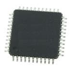
ICGOO电子元器件商城为您提供AD9481BSUZ-250由Analog设计生产,在icgoo商城现货销售,并且可以通过原厂、代理商等渠道进行代购。 AD9481BSUZ-250价格参考。AnalogAD9481BSUZ-250封装/规格:数据采集 - 模数转换器, 8 Bit Analog to Digital Converter 1 Input 1 Pipelined 44-TQFP (10x10)。您可以下载AD9481BSUZ-250参考资料、Datasheet数据手册功能说明书,资料中有AD9481BSUZ-250 详细功能的应用电路图电压和使用方法及教程。
AD9481BSUZ-250是Analog Devices Inc.生产的一款高速模数转换器(ADC),主要应用于需要高精度和高速数据采集的场景。其典型应用场景包括:

1. 通信系统:用于软件定义无线电(SDR)、基站接收器和无线基础设施,能够处理高频信号,实现高效的数据转换。

2. 测试与测量设备:广泛应用于示波器、频谱分析仪和信号发生器等仪器中,提供高精度信号采集和分析能力。

3. 工业控制与自动化:在高精度传感器信号采集、过程监控和自动化控制系统中,用于将模拟信号快速准确地转换为数字信号,便于后续处理和分析。

4. 医疗成像设备:如超声波、CT和MRI设备中的信号采集部分,要求高分辨率和高速度,AD9481可满足此类需求。

5. 雷达与国防电子系统:用于雷达接收机和电子战系统中,实现对复杂信号的快速采集与处理。

该ADC具有16位分辨率和250MSPS采样率,支持宽输入带宽和良好的线性度,适合对性能要求较高的高端应用。
| 参数 | 数值 |
| 产品目录 | 集成电路 (IC)半导体 |
| 描述 | IC ADC 8BIT 250MSPS 3.3V 44-TQFP模数转换器 - ADC 8 Bit 250 Msps 3.3V |
| DevelopmentKit | AD9481-PCBZ |
| 产品分类 | |
| 品牌 | Analog Devices |
| 产品手册 | |
| 产品图片 |
|
| rohs | 符合RoHS无铅 / 符合限制有害物质指令(RoHS)规范要求 |
| 产品系列 | 数据转换器IC,模数转换器 - ADC,Analog Devices AD9481BSUZ-250- |
| 数据手册 | |
| 产品型号 | AD9481BSUZ-250 |
| 产品目录页面 | |
| 产品种类 | 模数转换器 - ADC |
| 位数 | 8 |
| 供应商器件封装 | 44-TQFP(10x10) |
| 信噪比 | 46 dB |
| 其它名称 | AD9481BSUZ250 |
| 分辨率 | 8 bit |
| 包装 | 托盘 |
| 商标 | Analog Devices |
| 安装类型 | 表面贴装 |
| 安装风格 | SMD/SMT |
| 封装 | Tray |
| 封装/外壳 | 44-TQFP |
| 封装/箱体 | TQFP-44 |
| 工作温度 | -40°C ~ 85°C |
| 工作电源电压 | 3.3 V |
| 工厂包装数量 | 160 |
| 接口类型 | Parallel, LVDS |
| 数据接口 | 并联 |
| 最大功率耗散 | 618.8 mW |
| 最大工作温度 | + 85 C |
| 最小工作温度 | - 40 C |
| 标准包装 | 1 |
| 电压参考 | Internal, External |
| 电压源 | 单电源 |
| 系列 | AD9481 |
| 结构 | Pipeline |
| 转换器数 | 1 |
| 转换器数量 | 1 |
| 转换速率 | 250 MS/s |
| 输入数和类型 | 2 个单端,单极2 个差分,单极 |
| 输入类型 | Differential |
| 通道数量 | 1 Channel |
| 配用 | /product-detail/zh/AD9481-PCBZ/AD9481-PCBZ-ND/1534568 |
| 采样率(每秒) | 250M |


PDF Datasheet 数据手册内容提取
8-Bit, 250 MSPS 3.3 V A/D Converter AD9481 FEATURES FUNCTIONAL BLOCK DIAGRAM DNL = ±0.35 LSB VREF SENSE AGND DRGND DRVDD AVDD INL = ±0.26 LSB Single 3.3 V supply operation (3.0 V to 3.6 V) AD9481 REFERENCE Power dissipation of 439 mW at 250 MSPS PORT 8 A D7A TO D0A 1 V p-p analog input range VIN+ 8-BIT Internal 1.0 V reference VIN– T AND H ADC 8 SDien-gmleu-letinpdleexde odr CdMiffOeSre onuttiaplu atns alog inputs DS+ PICPOELRIENE POBRT 8 D7B TO D0B DS– Power-down mode CLK+ CLOCK DCO+ Clock duty cycle stabilizer MGMT CLK– DCO– LOGIC APPLICATIONS Digital oscilloscopes PDWN S1 05045-001 Instrumentation and measurement Figure 1. Communications Point-to-point radios Digital predistortion loops GENERAL DESCRIPTION The AD9481 is available in a Pb-free, 44-lead, surface-mount package (TQFP-44) specified over the industrial temperature The AD9481 is an 8-bit, monolithic analog-to-digital converter range (−40°C to +85°C). (ADC) optimized for high speed and low power consumption. Small in size and easy to use, the product operates at a PRODUCT HIGHLIGHTS 250 MSPS conversion rate, with excellent linearity and dynamic 1. Superior linearity. A DNL of ±0.35 makes the AD9481 performance over its full operating range. suitable for many instrumentation and measurement To minimize system cost and power dissipation, the AD9481 applications includes an internal reference and track-and-hold circuit. The 2. Power-down mode. A power-down function may be exercised user only provides a 3.3 V power supply and a differential to bring total consumption down to 15 mW. encode clock. No external reference or driver components are required for many applications. 3. De-multiplexed CMOS outputs allow for easy interfacing with low cost FPGAs and standard logic. The digital outputs are TTL/CMOS-compatible with an option of twos complement or binary output format. The output data bits are provided in an interleaved fashion along with output clocks that simplifies data capture. Rev. 0 Information furnished by Analog Devices is believed to be accurate and reliable. However, no responsibility is assumed by Analog Devices for its use, nor for any infringements of patents or other rights of third parties that may result from its use. One Technology Way, P.O. Box 9106, Norwood, MA 02062-9106, U.S.A. Specifications subject to change without notice. No license is granted by implication or otherwise under any patent or patent rights of Analog Devices. Trademarks and Tel: 781.329.4700 www.analog.com registered trademarks are the property of their respective owners. Fax: 781.326.8703 © 2004 Analog Devices, Inc. All rights reserved.
AD9481 TABLE OF CONTENTS DC Specifications.............................................................................3 Data Clock Out...........................................................................20 Digital Specifications........................................................................4 Power-Down Input.....................................................................20 AC Specifications..............................................................................5 AD9481 Evaluation Board............................................................21 Switching Specifications..................................................................6 Power Connector........................................................................21 Timing Diagram...........................................................................7 Analog Inputs..............................................................................21 Absolute Maximum Ratings............................................................8 Gain..............................................................................................21 Explanation of Test Levels...........................................................8 Optional Operational Amplifier...............................................21 ESD Caution..................................................................................8 Clock............................................................................................21 Pin Configuration and Function Descriptions.............................9 Optional Clock Buffer...............................................................21 Terminology....................................................................................10 DS.................................................................................................21 Typical Performance Characteristics...........................................12 Optional XTAL...........................................................................22 Equivalent Circuits.........................................................................16 Voltage Reference.......................................................................22 Applications.....................................................................................17 Data Outputs...............................................................................22 Analog Inputs..............................................................................17 Evaluation Board Bill of Materials (BOM).................................23 Voltage Reference.......................................................................17 PCB Schematics..............................................................................24 Clocking the AD9481.................................................................19 PCB Layers......................................................................................26 DS Inputs.....................................................................................19 Outline Dimensions.......................................................................28 Digital Outputs...........................................................................20 Ordering Guide..........................................................................28 Interleaving Two AD9481s........................................................20 REVISION HISTORY 10/04—Revision 0: Initial Version Rev. 0 | Page 2 of 28
AD9481 DC SPECIFICATIONS AVDD = 3.3 V, DRVDD = 3.3 V; T = −40°C, T = +85°C, A = −1 dBFS, full scale = 1.0 V, internal reference, differential analog and MIN MAX IN clock inputs, unless otherwise noted. Table 1. AD9481-250 Parameter Temp Test Level Min Typ Max Unit RESOLUTION 8 Bits ACCURACY No Missing Codes Full VI Guaranteed Offset Error 25°C I −40 40 mV Gain Error1 25°C I −6.0 6.0 % FS Differential Nonlinearity (DNL) Full VI −0.85 ±0.35 0.85 LSB Integral Nonlinearity (INL) Full VI −0.9 ±0.26 0.9 LSB TEMPERATURE DRIFT Offset Error Full V 30 µV/°C Gain Error Full V 0.03 % FS/°C Reference Full V ±0.025 mV/°C REFERENCE Internal Reference Voltage Full VI 0.97 1.0 1.03 V Output Current2 25°C IV 1.5 mA I Input Current3 25°C I 100 µA VREF I Input Current2 25°C I 10 µA SENSE ANALOG INPUTS (VIN+, VIN−) Differential Input Voltage Range4 Full V 1 V p-p Common-Mode Voltage Full VI 1.6 1.9 2.1 V Input Resistance Full VI 8.4 10 11.2 kΩ Input Capacitance 25°C V 4 pF Analog Bandwidth, Full Power 25°C V 750 MHz POWER SUPPLY AVDD Full IV 3.0 3.3 3.6 V DRVDD Full IV 3.0 3.3 3.6 V Supply Currents IAVDD5 Full VI 133 145 mA IDRVDD5 Full VI 39 42.5 mA Power Dissipation5 25°C V 439 mW Power-Down Dissipation 25°C V 15 37 mW Power Supply Rejection Ratio (PSRR) 25°C V −4.2 mV/V 1 Gain error and gain temperature coefficients are based on the ADC only (with a fixed 1 V external reference and 1 V p-p input range). 2 Internal reference mode; SENSE = AGND. 3 External reference mode; VREF driven by external 1.0 V reference; SENSE = AVDD. 4 In FS = 1 V, both analog inputs are 500 mV p-p and out of phase with each other. 5 Supply current measured with rated encode and a 20 MHz analog input. Power dissipation measured with dc input, see the Terminology section for power vs. clock rate. Rev. 0 | Page 3 of 28
AD9481 DIGITAL SPECIFICATIONS AVDD = 3.3 V, DRVDD = 3.3 V; T = −40°C, T = +85°C, A = −1 dBFS, full scale = 1.0 V, internal reference, differential analog and MIN MAX IN clock inputs, unless otherwise noted. Table 2. AD9481-250 Parameter Temp Test Level Min Typ Max Unit CLOCK AND DS INPUTS (CLK+, CLK−, DS+, DS−) Differential Input Full IV 200 mV p-p Common-Mode Voltage1 Full VI 1.38 1.5 1.68 V Input Resistance Full VI 4.2 5.5 6.0 kΩ Input Capacitance 25°C V 4 pF LOGIC INPUTS (PDWN, S1) Logic 1 Voltage Full IV 2.0 V Logic 0 Voltage Full IV 0.8 V Logic 1 Input Current Full VI ±160 µA Logic 0 input Current Full VI 10 µA Input Resistance 25°C V 30 kΩ Input Capacitance 25°C V 4 pF DIGITAL OUTPUTS Logic 1 Voltage2 Full VI DRVDD − 0.05 mV Logic 0 Voltage Full VI 0.05 V Output Coding Full IV Twos complement or binary 1 The common mode for CLOCK inputs can be externally set, such that 0.9 V < CLK ± < 2.6 V. 2 Capacitive loading only. Rev. 0 | Page 4 of 28
AD9481 AC SPECIFICATIONS AVDD = 3.3 V, DRVDD = 3.3 V; T = −40°C, T = +85°C, A = −1 dBFS, full scale = 1.0 V, internal reference, differential analog and MIN MAX IN clock inputs, unless otherwise noted. Table 3. AD9481-250 Parameter Temp Test Level Min Typ Max Unit SIGNAL-TO-NOISE RATIO (SNR) f = 19.7 MHz 25°C V 46 dB IN f = 70.1 MHz 25°C I 44.5 45.7 dB IN SIGNAL-TO-NOISE AND DISTORTION (SINAD) f = 19.7 MHz 25°C V 45.9 dB IN f = 70.1 MHz 25°C I 44.4 45.7 dB IN EFFECTIVE NUMBER OF BITS (ENOB) f = 19.7 MHz 25°C V 7.5 Bits IN f = 70.1 MHz 25°C I 7.2 7.5 Bits IN WORST SECOND OR THIRD HARMONIC DISTORTION f = 19.7 MHz 25°C V −64.8 dBc IN f = 70.1 MHz 25°C I −64.8 −54 dBc IN WORST OTHER f = 19.7 MHz 25°C V −68 dBc IN f = 70.1 MHz 25°C I −65.8 −56 dBc IN SPURIOUS-FREE DYNAMIC RANGE (SFDR)1 f = 19.7 MHz 25°C V −64.8 dBc IN f = 70.1 MHz 25°C I −64.8 −54 dBc IN TWO-TONE INTERMODULATION DISTORTION (IMD) f = 69.3 MHz, f = 70.3 MHz 25°C V −64.9 dBc IN1 IN2 1 DC and Nyquist bin energy ignored. Rev. 0 | Page 5 of 28
AD9481 SWITCHING SPECIFICATIONS AVDD = 3.3 V, DRVDD = 3.3 V; differential encode input, duty cycle stabilizer enabled, unless otherwise noted. Table 4. AD9481-250 Parameter Temp Test Level Min Typ Max Unit CLOCK Maximum Conversion Rate Full VI 250 MSPS Minimum Conversion Rate Full IV 20 MSPS Clock Pulse-Width High (t ) Full IV 1.2 2 ns EH Clock Pulse-Width Low (t ) Full IV 1.2 2 ns EL DS Input Setup Time (t ) Full IV 0.5 ns SDS DS Input Hold Time (t ) Full IV 0.5 ns HDS OUTPUT PARAMETERS1 Valid Time (t)2 Full VI 2.5 ns V Propagation Delay (t ) Full VI 4 5.4 ns PD Rise Time (t) 10% to 90% Full V 670 ps R Fall Time (t) 10% to 90% Full V 360 ps F DCO Propagation Delay (t ) 3 Full VI 2.5 3.9 5.3 ns CPD Data-to-DCO Skew (t − t )4 Full VI −0.5 +0.5 ns PD CPD A Port Data to DCO− Rising (t )5 Full IV 4 ns SKA B Port Data to DCO+ Rising (t ) Full IV 4 ns SKB Pipeline Latency (A, B) Full IV 8 Cycles APERTURE Aperture Delay (t ) 25°C V 1.5 ns A Aperture Uncertainty (Jitter) 25°C V 0.25 ps rms OUT-OF-RANGE RECOVERY TIME 25°C V 1 Cycle 1 CLOAD equals 5 pF maximum for all output switching specifications. 2 Valid time is approximately equal to minimum tPD. 3 TCPD equals clock rising edge to DCO (+ or −) rising edge delay. 4 Data changing to (DCO+ or DCO−) rising edge delay. 5 TSKA, TSKB are both clock rate dependent delays equal to TCYCLE − (Data to DCO skew). Rev. 0 | Page 6 of 28
AD9481 TIMING DIAGRAM N–1 N+9 t A N N+8 N+10 VIN N+1 N+7 8 CYCLES t t EH EL 1/fS CLK+ CLK– t HDS DS+ DS– t SDS t V INTERLEAVED DATA OUT t PD PORT A STATIC INVALID N D7A TO D0A PORT B STATIC INVALID INVALID N+1 D7B TO D0B t SKA t t SKB CPD DDCCOO+– STATIC 05045-002 Figure 2. Timing Diagram Rev. 0 | Page 7 of 28
AD9481 ABSOLUTE MAXIMUM RATINGS Thermal impedance (θ ) = 46.4°C/W (4-layer PCB). EXPLANATION OF TEST LEVELS JA Table 5. Table 6. Min. Max. Level Description Parameter Rating Rating I 100% production tested. ELECTRICAL II 100% production tested at 25°C and guaranteed by AVDD (With respect to AGND) −0.5 V +4.0 V design and characterization at specified temperatures. DRVDD −0.5 V +4.0 V III Sample tested only. (With respect to DRGND) IV Parameter is guaranteed by design and characterization AGND (With respect to DRGND) −0.5 V +0.5 V testing. Digital I/0 −0.5 V DRVDD + 0.5 V V Parameter is a typical value only. (With respect to DRGND) VI 100% production tested at 25°C and guaranteed by Analog Inputs −0.5 V AVDD + 0.5 V design and characterization for industrial temperature (With respect to AGND) range. ENVIRONMENTAL Operating Temperature −40°C +85°C Junction Temperature 150°C Storage Temperature 150°C Stresses above those listed under Absolute Maximum Ratings may cause permanent damage to the device. This is a stress rating only; functional operation of the device at these or any other conditions above those indicated in the operational section of this specification is not implied. Exposure to absolute maximum rating conditions for extended periods may affect device reliability. ESD CAUTION ESD (electrostatic discharge) sensitive device. Electrostatic charges as high as 4000 V readily accumulate on the human body and test equipment and can discharge without detection. Although this product features proprietary ESD protection circuitry, permanent damage may occur on devices subjected to high energy electrostatic discharges. Therefore, proper ESD precautions are recommended to avoid performance degradation or loss of functionality. Rev. 0 | Page 8 of 28
AD9481 PIN CONFIGURATION AND FUNCTION DESCRIPTIONS DS+ DS– S3 AVDD AGND VIN+ VIN– AGND AVDD AGND VREF 44 43 42 41 40 39 38 37 36 35 34 CLK+ 1 33 SENSE CLK– 2 PIN 1 32 AGND AVDD 3 31 AVDD AGND 4 AD9481 30 AVDD DRVDD 5 TOP VIEW 29 PDWN DRGND 6 (Not to Scale) 28 S1 D7A (MSB) 7 27 DRGND D6A 8 26 D7B (MSB) D5A 9 25 D6B D4A 10 24 D5B D3A 11 23 D4B 12 13 14 15 16 17 18 19 20 21 22 D2A D1A A (LSB) DRGND DCO– DCO+ DRVDD B (LSB) D1B D2B D3B 05045-003 D0 D0 Figure 3. Pin Configuration Table 7. Pin Function Descriptions Pin Pin No. Name Description No. Name Description 1 CLK+ Input Clock—True 25 D6B Data Output Bit 6—Channel B 2 CLK− Input Clock—Complement 26 D7B Data Output Bit 7—Channel B (MSB) 3 AVDD 3.3 V Analog Supply 27 DRGND Digital Ground 4 AGND Analog Ground 28 S1 Data Format Select and Duty Cycle Stabilizer 5 DRVDD 3.3 V Digital Output Supply Select 6 DRGND Digital Ground 29 PDWN Power-Down Selection 7 D7A Data Output Bit 7—Channel A (MSB) 30 AVDD 3.3 V Analog Supply 8 D6A Data Output Bit 6—Channel A 31 AVDD 3.3 V Analog Supply 9 D5A Data Output Bit 5—Channel A 32 AGND Analog Ground 10 D4A Data Output Bit 4—Channel A 33 SENSE Reference Mode Selection 11 D3A Data Output Bit 3—Channel A 34 VREF Voltage Reference Input/Output 12 D2A Data Output Bit 2—Channel A 35 AGND Analog Ground 13 D1A Data Output Bit 1—Channel A 36 AVDD 3.3 V Analog Supply 14 D0A Data Output Bit 0—Channel A (LSB) 37 AGND Analog Ground 15 DRGND Digital Ground 38 VIN− Analog Input—Complement 16 DCO− Data Clock Output—Complement 39 VIN+ Analog Input—True 17 DCO+ Data Clock Output—True 40 AGND Analog Ground 18 DRVDD 3.3 V Digital Output Supply 41 AVDD 3.3 V Analog Supply 19 D0B Data Output Bit 0—Channel B (LSB) 42 S3 DCO Enable Select (Tie to AVDD for DCO Active) 20 D1B Data Output Bit 1—Channel B 43 DS− Data Sync Complement (If Unused, Tie to 21 D2B Data Output Bit 2—Channel B DRVDD) 22 D3B Data Output Bit 3—Channel B 44 DS+ Data Sync True (If Unused, Tie to DGND) 23 D4B Data Output Bit 4—Channel B 24 D5B Data Output Bit 5—Channel B Rev. 0 | Page 9 of 28
AD9481 TERMINOLOGY Analog Bandwidth Full-Scale Input Power The analog input frequency at which the spectral power of the Expressed in dBm. Computed using the following equation fundamental frequency (as determined by the FFT analysis) is reduced by 3 dB. ⎜⎛V2FULLSCALErms⎟⎞ ⎜ Z ⎟ Aperture Delay PowerFULLSCALE=10log⎜ 0I.N0P0U1T ⎟ The delay between the 50% point of the rising edge of the ⎜ ⎟ ⎜ ⎟ encode command and the instant the analog input is sampled. ⎝ ⎠ Aperture Uncertainty (Jitter) Gain Error The sample-to-sample variation in aperture delay. Gain error is the difference between the measured and ideal full-scale input voltage range of the ADC. Clock Pulse-Width/Duty Cycle Pulse-width high is the minimum amount of time that the clock Harmonic Distortion, Second pulse should be left in a Logic 1 state to achieve rated The ratio of the rms signal amplitude to the rms value of the performance; pulse-width low is the minimum time clock pulse second harmonic component, reported in dBc. should be left in a low state. See timing implications of changing Harmonic Distortion, Third t in the Clocking the AD9481 section. At a given clock rate, EH The ratio of the rms signal amplitude to the rms value of the these specifications define an acceptable clock duty cycle. third harmonic component, reported in dBc. Crosstalk Integral Nonlinearity Coupling onto one channel being driven by a low level The deviation of the transfer function from a reference line (−40 dBFS) signal when the adjacent interfering channel is measured in fractions of 1 LSB using a best straight line driven by a full-scale signal. determined by a least square curve fit. Differential Analog Input Resistance, Differential Analog Minimum Conversion Rate Input Capacitance, and Differential Analog Input Impedance The encode rate at which the SNR of the lowest analog signal The real and complex impedances measured at each analog frequency drops by no more than 3 dB below the guaranteed input port. The resistance is measured statically and the limit. capacitance and differential input impedances are measured with a network analyzer. Maximum Conversion Rate The encode rate at which parametric testing is performed. Differential Analog Input Voltage Range The peak-to-peak differential voltage that must be applied to Output Propagation Delay the converter to generate a full-scale response. Peak differential The delay between a differential crossing of CLK+ and CLK− voltage is computed by observing the voltage on a single pin and the time when all output data bits are within valid logic and subtracting the voltage from the other pin, which is 180° levels. out of phase. Peak-to-peak differential is computed by rotating the inputs phase 180° and taking the peak measurement again. Noise (for Any Range within the ADC) The difference is then computed between both peak This value includes both thermal and quantization noise. measurements. ⎛FS −SNR −Signal ⎞ Differential Nonlinearity Vnoise = Z×0.001×10⎜⎜⎝ dBm d1B0c dBFS ⎟⎟⎠ The deviation of any code width from an ideal 1 LSB step. where: Effective Number of Bits (ENOB) ENOB is calculated from the measured SINAD based on the Z is the input impedance. equation (assuming full-scale input) FS is the full scale of the device for the frequency in question. SINAD −1.76dB ENOB= MEASURED 6.02 SNR is the value for the particular input level. Signal is the signal level within the ADC reported in dB below full scale. Rev. 0 | Page 10 of 28
AD9481 Power Supply Rejection Ratio Two-Tone SFDR The ratio of a change in input offset voltage to a change in The ratio of the rms value of either input tone to the rms value power supply voltage. of the peak spurious component. The peak spurious component may or may not be an IMD product. It also may be reported in Signal-to-Noise and Distortion (SINAD) dBc (degrades as signal level is lowered) or in dBFS (always The ratio of the rms signal amplitude (set 1 dB below full scale) relates back to converter full scale). to the rms value of the sum of all other spectral components, including harmonics, but excluding dc. Worst Other Spur The ratio of the rms signal amplitude to the rms value of the Signal-to-Noise Ratio (without Harmonics) worst spurious component (excluding the second and third The ratio of the rms signal amplitude (set at 1 dB below full harmonic), reported in dBc. scale) to the rms value of the sum of all other spectral components, excluding the first five harmonics and dc. Transient Response Time The time it takes for the ADC to reacquire the analog input Spurious-Free Dynamic Range (SFDR) after a transient from 10% above negative full scale to 10% The ratio of the rms signal amplitude to the rms value of the below positive full scale. peak spurious spectral component. The peak spurious component may or may not be a harmonic. It also may be Out-of-Range Recovery Time reported in dBc (degrades as signal level is lowered) or dBFS This is the time it takes for the ADC to reacquire the analog (always related back to converter full scale). input after a transient from 10% above positive full scale to 10% above negative full scale, or from 10% below negative full scale Two-Tone Intermodulation Distortion Rejection to 10% below positive full scale. The ratio of the rms value of either input tone to the rms value of the worst third-order intermodulation product, in dBc. Rev. 0 | Page 11 of 28
AD9481 TYPICAL PERFORMANCE CHARACTERISTICS AVDD, DRVDD = 3.3 V, T = 25°C, A differential drive, FS = 1, internal reference mode, unless otherwise noted. IN 0 0 SNR = 45.8dB SNR = 45.6dB –10 H2 =–65.2dBc –10 H2 =–72.9dBc H3 =–63.2dBc H3 =–65.2dBc SFDR = 63.2dBc SFDR = 59.6dBc –20 –20 –30 –30 –40 –40 B) B) d d ( –50 ( –50 –60 –60 –70 –70 ––9800 05045-004 ––9800 05045-007 0 20 40 60 80 100 120 0 20 40 60 80 100 120 (MHz) (MHz) Figure 4. FFT: fS = 250 MSPS, AIN = 10.3 MHz @ −1 dBFS Figure 7. FFT: fS = 250 MSPS, AIN = 170 MHz @ −1 dBFS 0 90 SNR = 45.8dB –10 H2 =–68.5dBc 85 H3 =–63.5dBc SFDR = 63.8dBc 80 –20 H3 75 –30 H2 70 –40 B) B) 65 d d ( –50 ( 60 –60 55 SFDR –70 50 SNR ––9800 05045-005 4450 SINAD 05045-008 0 20 40 60 80 100 120 0 50 100 150 200 250 300 350 400 (MHz) AIN (MHz) Figure 5. FFT: fS = 250 MSPS, AIN = 70 MHz @ −1 dBFS Figure 8. Analog Input Frequency Sweep, AIN = −1 dBFS, FS = 1 V, fS = 250 MSPS 0 90 SNR = 45.9dB –10 H2 =–66.6dBc 85 H3 =–70.1dBc SFDR = 65.9dBc 80 –20 H3 75 –30 H2 70 –40 B) B) 65 d d ( –50 ( 60 –60 SFDR 55 –70 50 ––9800 05045-006 4450 SNR SINAD 05045-009 0 20 40 60 80 100 120 0 50 100 150 200 250 300 350 400 (MHz) AIN (MHz) Figure 6. FFT: fS = 250 MSPS, AIN = 70 MHz @ −1 dBFS, Single-Ended Input Figure 9. Analog Input Frequency Sweep, AIN =−1 dBFS, FS = 0.75 V, fS = 250 MSPS, External VREF Mode Rev. 0 | Page 12 of 28
AD9481 75 140 70 IAVDD 120 SFDR 65 100 A) m 60 T ( 80 (dB) 55 RREN 60 U C 50 40 SNR IDRVDD 44500 50 100SINAD150 200 250 30005045-010 2000 50 100 150 200 250 30005045-013 SAMPLE CLOCK (MHz) SAMPLE CLOCK (MSPS) Figure 10. SNR, SINAD, SFDR vs. Sample Clock Frequency, Figure 13. IAVDD and IDRVDD vs. Clock Rate, CLOAD = 5 pF AIN = 70 MHz @ −1 dB AIN = 70 MHz @ −1 dBFS 80 50 49 70 SFDR (dBFS) 48 60 DCS ON 47 50 46 B) 40 B) 45 d d ( SFDR (dBc) ( 44 30 DCS OFF 43 20 60dB 42 REFERENCE LINE 100 05045-011 4401 05045-014 –70 –60 –50 –40 –30 –20 –10 0 20 30 40 50 60 70 80 ANALOG INPUT DRIVE LEVEL (dBFS) CLOCK POSITIVE DUTY CYCLE (%) Figure 11. SFDR vs. AIN Input Level; AIN = 70 MHz @ 250 MSPS Figure 14. SNR, SINAD vs. Clock Pulse-Width High, AIN = 70 MHz @ −1 dBFS, 250 MSPS, DCS On/Off 0 50.0 75 F1, F2 =–7dBFS –10 2F2–F1 =–65.9dBc 2F1–F2 =–64.9dBc –20 SNR 47.5 70 –30 B) –40 D (d SINAD Bc) (dB) –50 SINA 45.0 65 DR (d R, SFDR SF N –60 S 42.5 60 –70 ––9800 05045-012 40.0 55 05045-015 0 20 40 60 80 100 120 0.5 0.7 0.9 1.1 1.3 1.5 1.7 1.9 (MHz) EXTERNAL VREF VOLTAGE (V) Figure 12. Two-Tone Intermodulation Distortion Figure 15. SNR, SINAD, and SFDR vs. VREF in External Reference Mode, AIN = (69.3 MHz and 70.3 MHz; fS = 250 MSPS) 70 MHz @ −1 dBFS, 250 MSPS Rev. 0 | Page 13 of 28
AD9481 2.0 70 1.5 FS = 1V EXTERNAL REFERENCE 65 1.0 SFDR %) 0.5 R ( 60 O R 0 B) R d E ( N 55 AI –0.5 G –1.0 FS = 1V 50 INTERNAL REFERENCE SINAD ––21..05 05045-016 45 SNR 05045-019 –40 –20 0 20 40 60 80 3.0 3.1 3.2 3.3 3.4 3.5 3.6 TEMPERATURE (°C) AVDD (V) Figure 16. Full-Scale Gain Error vs. Temperature, Figure 19. SNR, SINAD, and SFDR vs. Supply Voltage, AIN = 70.3 MHz @ −0.5 dBFS, 250 MSPS AIN = 70.3 MHz @ −1 dBFS, 250 MSPS 70 0.5 0.4 65 0.3 SFDR 0.2 60 0.1 (dB) 55 LSB 0 –0.1 50 –0.2 SINAD –0.3 45 40 05045-017 ––00..54 05045-020 –40 –20 0 20 40 60 80 0 50 100 150 200 250 TEMPERATURE (°C) CODE Figure 17. SINAD, SFDR vs. Temperature, Figure 20. Typical DNL Plot, AIN = 70 MHz @ −1 dBFS, 250 MSPS AIN = 10.3 MHz @ −0.5 dBFS, 250 MSPS 0.10 0.50 0.05 0.25 %) EF ( 0 R N V SB 0 E I L G–0.05 N A H C –0.25 –0.10 –0.15 05045-018 –0.50 05045-021 2.7 2.8 2.9 3.0 3.1 3.2 3.3 3.4 3.5 3.6 0 50 100 150 200 250 AVDD (V) CODE Figure 18. VREF Sensitivity to AVDD Figure 21. Typical INL Plot, AIN = 10.3 MHz @ −0.5 dBFS, 250 MSPS Rev. 0 | Page 14 of 28
AD9481 TPD_F 0.2 0.1 s) TCPD_F p E ( 0 G N A CH –0.1 Y A L DE –0.2 TCPD_R –0.3 –0.4 TPD_R 05045-048 –40 –20 0 20 40 60 80 TEMPERATURE (°C) Figure 22. Propagation Delay Sensitivity vs. Temperature Rev. 0 | Page 15 of 28
AD9481 EQUIVALENT CIRCUITS AVDD AVDD 16.7kΩ 16.7kΩ 150Ω 150Ω VIN+ VIN– PDWN 25kΩ 1.2pF 25kΩ 1.2pF 30kΩ 05045-023 05045-026 Figure 23. Analog Inputs Figure 26. Power-Down Input AVDD DRVDD 12kΩ 12kΩ CLK+ CLK– 150Ω 150Ω 10kΩ 10kΩ 05045-027 Figure 27. Data, DCO Outputs 05045-024 Figure 24. Clock Inputs VDD 30kΩ S1 05045-025 Figure 25. S1 Input Rev. 0 | Page 16 of 28
AD9481 APPLICATIONS The AD9481 uses a 1.5 bit per stage architecture. The analog inputs drive an integrated high bandwidth track-and-hold 49.9Ω 499Ω circuit that samples the signal prior to quantization by the 8-bit AVDD 33Ω core. For ease of use, the part includes an on-board reference 499Ω VIN+ and input logic that accepts TTL, CMOS, or LVPECL levels. The 1.3kΩ AD8138 20pF AD9481 33Ω digital output logic levels are CMOS-compatible. 523Ω VIN– ANALOG INPUTS 0.1µF 2kΩ 499Ω AGND 05045-030 The analog input to the AD9481 is a differential buffer. For best Figure 29. Driving the ADC with the AD8138 dynamic performance, impedances at VIN+ and VIN− should The AD9481 can be easily configured for different full-scale match. Optimal performance is obtained when the analog ranges. See the Voltage Reference section for more information. inputs are driven differentially. SNR and SINAD performance Optimal performance is achieved with a 1 V p-p analog input. can degrade if the analog input is driven with a single-ended signal. The analog inputs self-bias to approximately 1.9 V; this SENSE = GND common-mode voltage can be externally overdriven by approximately ±300 mV if required. A wideband transformer, such as the Mini-Circuits ADT1-1WT, VIN+ can provide the differential analog inputs for applications that require a single-ended-to-differential conversion. Note that the 500mV 2.0V 2.0V filter and center-tap capacitor on the secondary side is optional and dependent on application requirements. An RC filter at the VIN– secondary side helps reduce any wideband noise getting aliased by the ADC. DIGITALOUT = ALL 1s DIGITALOUT = ALL 0s (R, C OPTIONAL) AVDD 05045-031 33Ω VIN+ Figure 30. Analog Input Full Scale 49.9Ω 10pF AD9481 VOLTAGE REFERENCE 33Ω VIN– A stable and accurate 1.0 V reference is built into the AD9481. AGND 0.1µF 05045-029 Uresfeerrse nccaen fcohro gorseea ttehri sa cinctuerrancayl arnefde rfelenxcieb iolirt yp.r Foivgiudree a 3n2 e sxhtoerwnsa l Figure 28. Driving the ADC with an RF Transformer the typical reference variation with temperature. Table 8 summarizes the available reference configurations. For dc-coupled applications, the AD8138/AD8139 or AD8351 can serve as a convenient ADC driver, depending on VIN+ requirements. Figure 29 shows an example with the AD8138. VIN– The AD9481 PCB has an optional AD8351 on board, as shown in Figure 39 and Figure 40. The AD8351 typically yields better performance for frequencies greater than 30 MHz to 40 MHz. ADC CORE The AD9481’s linearity and SFDR start to degrade at higher analog frequencies (see the Typical Performance Characteristics section). For higher frequency applications, the AD9480 with VREF LVDS outputs and superior AC performance should be + considered. 10µF 0.1µF 7kΩ SELECT LOGIC SENSE 7kΩ 0.5V 05045-032 Figure 31. Internal Reference Equivalent Circuit Rev. 0 | Page 17 of 28
AD9481 Fixed Reference The internal reference can be configured for a differential span of 1 V p-p (see Figure 34). It is recommended to place a 0.1 µF VREF capacitor as close as possible to the VREF pin; a 10 µF capacitor 10µF 0.1µF is also required (see the PCB layout for guidance). If the internal rimefperreonvcee g oafin t hme aAtcDh9in4g8,1 t hise u lsoeadd itnog d orfiv teh me ruelfteiprelen cceo nbvye trhteer s to SENSE 05045-034 other converters must be considered. Figure 34 depicts how the Figure 33. Internal Fixed Reference (1 V p-p) internal reference voltage is affected by loading. 0 1.0085 1.0080 E –0.1 G 1.0075 TA L O 1.0070 F V –0.2 E VREF (V)111...000000656055 ANGE IN VR –0.3 H C 1.0050 % –0.4 111...000000443505 05045-033 –0.50 0.5 1.0 IREF1. 5(mA) 2.0 2.5 3.005045-035 –40 –20 0 20 40 60 80 TEMPERATURE (°C) Figure 34. Internal VREF vs. Load Current Figure 32. Typical Reference Variation with Temperature Table 8. Reference Configurations SENSE Voltage Resulting VREF Reference Differential Span AVDD N/A (external reference input) External 1 × external reference voltage 0.5 V (Self-Biased) 0.5 × (1 + R1/R2) V Programmable 1 × VREF (0.75 V p-p to 1.5 V p-p) AGND to 0.2 V 1.0 V Internal fixed 1 V p-p Rev. 0 | Page 18 of 28
AD9481 External Reference change dynamically, requiring a wait time of 5 µs after a An external reference can be used for greater accuracy and dynamic clock frequency increase before valid data is available. temperature stability when required. The gain of the AD9481 The clock duty cycle stabilizer can be disabled at Pin 28 (S1). can also be varied using this configuration. A voltage output The clock inputs are internally biased to 1.5 V (nominal) and DAC can be used to set VREF, providing for a means to digitally support either differential or single-ended signals. For best adjust the full-scale voltage. VREF can be externally set to dynamic performance, a differential signal is recommended. An voltages from 0.75 V to 1.5 V; optimum performance is typically MC100LVEL16 performs well in the circuit to drive the clock obtained at VREF = 1 V. (See the Typical Performance inputs (ac coupling is optional). If the clock buffer is greater Characteristics section.) than two inches from the ADC, a standard LVPECL MAY REQUIRE termination may be required instead of the simple pull-down RC FILTER termination shown in Figure 37. EXTERNAL REFERENCE OR VREF DAC INPUT 0.1µF AD9481 AVDD CLK+ SENSE 05045--036 PGEACTLE CLK– 0.1µF Figure 35. External Reference 510kΩ 510kΩ PTrhoeg prraomgrmamabmlea bRlee freerfeernecnec e can be used to set a differential 05045-028 input span anywhere between 0.75 V p-p and 1.5 V p-p by using Figure 37. Clocking the AD9481 an external resistor divider. The SENSE pin self-biases to 0.5 V, DS INPUTS and the resulting VREF is equal to 0.5 × (1 + R1/R2). It is The data sync inputs (DS+, DS−) can be used in applications recommended to keep the sum of R1 + R2 ≥ 10 kΩ to limit which require that a given sample appear at a specific output VREF loading (for VREF = 1.5 V, set R1 equal to 7 kΩ and R2 port (A or B) relative to a given external timing signal. equal to 3.5 kΩ). The DS inputs can also be used to synchronize two or more ADCs in a system to maintain phasing between Ports A and B on VREF separate ADCs (in effect, synchronizing multiple DCO outputs). 10µF 0.1µF R1 The DS inputs are internally biased to 1.5 V (nominal) and R2 SENSE 05045-037 shuepldp ohrigt hei (thDeSr− d lioffwer)e, nthtiea Al oDr Csi ndgaltea- oenudtpeudt ss iagnnda lDs. CWOh eonu tDpSu+ts is do not switch and are held static. Synchronization is Figure 36. Programmable Reference accomplished by the assertion (falling edge) of DS+ within the CLOCKING THE AD9481 timing constraints t and t , relative to a clock rising edge. SDS HDS (On initial synchronization, t is not relevant.) If DS+ falls Any high speed ADC is extremely sensitive to the quality of the HDS within the required setup time (t ) before a given clock rising sampling clock provided by the user. A track-and-hold circuit is SDS edge N, the analog value at that point in time is digitized and essentially a mixer, and any noise, distortion, or timing jitter on available at Port A, eight cycles later in interleaved mode. The the clock is combined with the desired signal at the A/D output. next sample, N + 1, is sampled by the next rising clock edge and Considerable care has been taken in the design of the CLOCK available at Port B, eight cycles after that clock edge. input of the AD9481, and the user is advised to give commensurate thought to the clock source. Driving each ADC’s DS inputs by the same sync signal accomplishes synchronization between multiple ADCs. In The AD9481 has an internal clock duty cycle stabilization applications which require synchronization, one-shot circuit that locks to the rising edge of CLOCK and optimizes synchronization is recommended. An easy way to accomplish timing internally for sample rates between 100 MSPS and synchronization is by a one-time sync at power-on reset. 250 MSPS. This allows for a wide range of input duty cycles at the input without degrading performance. Jitter on the rising edge of the input is still of paramount concern and is not reduced by the internal stabilization circuit. The duty cycle control loop does not function for clock rates less than 70 MHz nominally. The loop has a time constant associated with it that needs to be considered in applications where the clock rate can Rev. 0 | Page 19 of 28
AD9481 Table 9. S1 Voltage Levels INTERLEAVING TWO AD9481s Duty Cycle Instrumentation applications may prefer to interleave (or ping- S1 Voltage Data Format Stabilizer pong) two AD9481s to achieve twice the sample rate, or (0.9 × AVDD)→AVDD Offset binary Disabled 500 MSPS. In these applications, it is important to match the (2/3 × AVDD) ± (0.1 × AVDD) Offset binary Enabled gain and offset of the two ADCs. Varying the reference voltage (1/3 × AVDD) ± (0.1 × AVDD) Twos complement Enabled allows the gain of the ADCs to be adjusted; external dc offset AGND → (0.1 × AVDD) Twos complement Disabled compensation can be used to reduce offset mismatch between two ADCs. The sampling phase offset between the two ADCs DIGITAL OUTPUTS is extremely important as well and requires very low skew The CMOS digital outputs are TTL-/CMOS-compatible for between clock signals driving the ADCs (< 2 ps clock skew lower power consumption. The outputs are biased from a for a 100 MHz analog input frequency). separate supply (DRVDD), allowing easy interface to external DATA CLOCK OUT logic. The outputs are CMOS devices that swing from ground to DRVDD (with no dc load). It is recommended to minimize the A data clock is available at DCO+ and DCO−. These clocks can capacitive load the ADC drives by keeping the output traces facilitate latching off-chip, providing a low skew clocking short (< 2 inch, for a total C < 5 pF). When operating in solution. The on-chip delay of the DCO clocks tracks with the LOAD CMOS mode, it is also recommended to place low value series on-chip delay of the data bits, (under similar loading) such that damping resistors on the data lines close to the ADC to reduce the variation between tPD and tCPD is minimized. It is switching transient effects on performance. recommended to keep the trace lengths on the data and DCO pins matched and 2 inches maximum. A series damping resistor Table 10. Output Coding (FS = 1 V) at the clock outputs is also recommended. The DCO outputs Code (VIN+) − (VIN−) Offset Binary Twos Complement can be disabled and placed in a high impedance state by tying 255 > +0.512 V 1111 1111 0111 1111 S3 to ground (tie to AVDD for DCO active). Switching both 255 +0.512 V 1111 1111 0111 1111 into and out of high impedance is accomplished in 4 ns from S3 254 +0.508 V 1111 1110 0111 1110 switching. • • • • • • • • POWER-DOWN INPUT 129 +0.004 V 1000 0001 0000 0001 The ADC can be placed into a low power state by setting the 128 +0.0 V 1000 0000 0000 0000 PDWN pin to AVDD. Time to go into (or come out of) power 127 −0.004 V 0111 1111 1111 1111 down equals 30 ns typically from PDWN switching. • • • • • • • • 2 −0.504 V 0000 0010 1000 0010 1 −0.508 V 0000 0001 1000 0001 0 −0.512 V 0000 0000 1000 0000 0 < −0.512 V 0000 0000 1000 0000 Rev. 0 | Page 20 of 28
AD9481 AD9481 EVALUATION BOARD The AD9481 evaluation board offers an easy way to test the ANALOG INPUTS device. It requires a clock source, an analog input signal, and a The evaluation board accepts a 700 mV p-p analog input signal 3.3 V power supply. The clock source is buffered on the board to centered at ground at SMB Connector J3. This signal is provide the clocks for the ADC and a data-ready signal. The terminated to ground through 50 Ω by R22. The input can be digital outputs and output clocks are available at an 80-pin alternatively terminated at the T1 transformer secondary by output connector, P3, P23. (Note that P3, P23 are represented R21 and R28. T1 is a wideband RF transformer that provides schematically as two 40-pin connectors, and this connector is the single-ended-to-differential conversion, allowing the ADC implemented as one 80-pin connector on the PCB.) The board to be driven differentially, minimizing even-order harmonics. has several different modes of operation and is shipped in the An optional transformer, T4, can be placed if desired (remove following configuration: T1, as shown in Figure 39 and Figure 40). • Offset binary The analog signal can be low-pass filtered by R21, C8 and R28, C9 at the ADC input. • Internal voltage reference GAIN POWER CONNECTOR Full scale is set by the sense jumper. This jumper applies a bias Power is supplied to the board via two detachable 4-pin power to the SENSE pin to vary the full-scale range; the default strips. position is SENSE = ground, setting the full scale to 1 V p-p. Table 11. Power Connector OPTIONAL OPERATIONAL AMPLIFIER Terminal Comments VDL (3.3 V) Output supply for external latches and data The PCB has been designed to accommodate an optional ready clock buffer ~ 30 mA AD8351 op amp that can serve as a convenient solution for dc- coupled applications. To use the AD8351 op amp, remove R29, AVDD1 3.3 V Analog supply for ADC ~ 140 mA R31, and C3. Populate R12, R17, and R36 with 25 Ω resistors, DRVDD1 3.3 V Output supply for ADC ~ 30 mA and populate C1, C21, C23, C31, C39, and C30 with 0.1 µF VCTRL1 3.3 V Supply for support clock circuitry ~ 60 mA capacitors. Populate R54, R10, and R11 with 10 Ω resistors, and Op amp, ext. ref Optional supply for op amp and ADR510 reference R34 and R32 with 1 kΩ resistors. Populate R15 with a 1.2 kΩ resistor and R14 with a 100 Ω resistor. Populate R37 with a 10 kΩ resistor. 1 AVDD, DRVDD, VDL, and VCTRL are the minimum required power connections. CLOCK The clock input is terminated to ground through 50 Ω at SMA Connector J1. The input is ac-coupled to a high speed differential receiver (LVEL16) that provides the required low jitter, fast edge rates needed for best performance. J1 input should be > 0.5 V p-p. Power to the LVEL16 is set to VCTRL (default) or AVDD by jumper placement at the device. OPTIONAL CLOCK BUFFER The PCB has been designed to accommodate the SNLVDS1 line driver. The SNLVDS1 is used as a high speed LVDS-level optional encode clock. To use this clock, please remove C2, C5, and C6. Place 0.1 µF capacitors on C34, C35, and C26. Place a 10 Ω resistor on R48, and place a 100 Ω resistor on R6. Place a 0 Ω resistor on both R49 and R53. For best results using the line driver, J1 input should be > 2.5 V p-p. DS The DS inputs are available on the PCB at J2 and J4. If driving DS+ externally, place a 0 Ω resistor at C48 and remove R53. Rev. 0 | Page 21 of 28
AD9481 OPTIONAL XTAL To use either crystal, populate C38 and C40 with 0.1 µF capaci- The PCB has been designed to accommodate an optional tors. Populate R48 and R49 with 0 Ω resistors. Place R50, R51, crystal oscillator that can serve as a convenient clock source. R59, and R60 with 1 kΩ resistors. Remove C6 and C5. If the The footprint can accept both through-hole and surface-mount Vectron VCC6 family crystal is being used, populate R57 with a devices, including Vectron XO-400 and Vectron VCC6 family 10 Ω resistor. If using the XO-400 crystal, place jumper E21 or oscillators. E22 to E23. VOLTAGE REFERENCE The AD9481 has an internal 1 V reference mode. The ADC uses OUT+ the internal 1 V reference as the default when sense is set to VCC ground. An optional on-board external 1.0 V reference (ADR510) can be used by setting the sense jumper to AVDD, by placing a jumper on E5 to E3, and by placing a 0 Ω resistor on R55. When using an external programmable reference, (R20, R30) remove the sense jumper. OUT– DATA OUTPUTS GND The ADC outputs are buffered on the PCB by LVT574 latches VCC 05045-038 orens itshtoe rdsa atta tohuet opuuttps.u Tt hpein las ttcoh m ouintpimutisz eh arevfel escetriioens st.e rminating Figure 38. XTAL Footprint Rev. 0 | Page 22 of 28
AD9481 EVALUATION BOARD BILL OF MATERIALS (BOM) Table 12. No. Quantity Reference Designator Device Package Value 1 24 C1 to C6, C10 to C12, C14 to C15, Capacitors 0402 0.1 µF C17 to C19, C22 to C29, C31, C48 to C49 2 1 C13 Capacitor Tantalum (3528) 10 µF 3 5 C32 to C36 Capacitors Tantalum (6032) 10 µF 4 4 J1 to J4 SMA SMA Degrees 5 3 P1, P12 to P13 4-pin power connectors Post Z5.531.3425.0 6 3 P1, P12 to P13 4-pin power connectors Detachable connector 25.602.5453.0 7 2 P3, P23 80-pin connectors Connector TSW-140-08-L-D-RA 8 7 R1, R5, R19, R22, R27, R35, R53 Resistors 0603 50 Ω 9 8 R2 to R4, R6 to R9, R18, R14 Resistors 0603 100 Ω 10 7 R13, R42 to R45, R32, R34 Resistors 0603 1 kΩ 11 2 R16, R52 Resistors 0603 130 Ω 12 2 R23, R24 Resistors 0603 510 Ω 13 2 R25, R26 Resistors 0603 82 Ω 14 2 R29, R31 Resistors 0603 00 Ω 15 2 R33, R37 Resistors 0603 10 kΩ 16 1 R46 Resistor 0603 2 kΩ 17 3 R12, R17, R36 Resistors 0603 25 Ω 18 1 R15 Resistor 0603 1.2 kΩ 19 3 R54, R10 to R11 Resistors 0603 10 Ω 20 2 RP1 to RP2 Resistor Pack 100 Ω Res. Array 742C163100JTR 21 4 U3, U5 to U6, U8 Resistor Pack 100 Ω 100 Ω Res. Array EXB-38V101JV 22 2 U4, U7 74LVT574 SO20 74LVT574WM 23 1 T1 Transformer CD542 ADT1-1WT 24 1 U1 AD8351 MSOP-10 Op Amp 25 1 U2 74VCX86 SO-14 XOR 26 1 U101 ADR510 SOT-23 Voltage Regulator 27 1 U91 VCC6PECL6 VCC6-QAB-250M000 Vectron Crystal 28 1 U12 AD9481 TQFP-44 ADC 29 1 U11 MC100-LVEL16D S08NB Clock Buffer 30 1 T21 ETC1-1-13 1-1 TX M/A-COM/ETC 1-1-13 31 11 C1, C7 to C9, C16, C20, C30, C31, C38 to C40 Capacitors 0402 X1 32 18 R20 to R21, R28, R30, R38 to R41, Resistors 0603 X1 R48 to R51, R55 to R60 33 16 E98 to E102, E73 to E84 Jumpers 1 Not placed. Rev. 0 | Page 23 of 28
AD9481 PCB SCHEMATICS R 040-54050 ORCTO OUTPUTGNDCONNECTOR P39P40GND163940DB7XP37P38DR+373815P35P36GNDDB6X3536DB7XP33P3414DB5X3334P31P32DB6X133132DB4XDB5XP29P30293012DB4XP27P28DB3X2728DB3XP25P2611DB2X2526DB2XP23P24102324DB1XP21P22DB1X21229DB0XP19P20DB0X1920P17P181718P15P161516VDLP13P141314P11P121112P10P9R40910P7P8XT+78P5P656P3P434R41P1P21X2P23GND NOTE: TWO 40 PIN OUTPUT CONNECTIMPLEMENTED AS ONE 80 PIN CONNE OUTPUTGNDCONNECTOR P39P40GND163940DA0XP37P38DR–373815P35P36GNDDA1X3536DA7XP33P3414DA2X3334P31P32DA6X133132DA3XDA5XP29P30293012DA4XP27P28DA4X2728DA3XP25P2611DA5X2526DA2XP23P24102324DA6XP21P22DA1X21229DA0XP19P20DA7X1920P17P181718P15P161516VDLP13P141314P11P121112P10P9R38910P7P8XT–78P5P656P3P434R39P1P2X12P3GND 100ΩRP1 LKLA 100ΩRP2 LKLA C C 1 2 3 4 5 6 7 8 1 2 3 4 5 6 7 8 L L D D V V 20 19 18 17 16 15 14 13 12 11 20 19 18 17 16 15 14 13 12 11 CCQ0Q1Q2Q3Q4Q5Q6Q7CK CCQ0Q1Q2Q3Q4Q5Q6Q7CK U4VT574 VN CLO U7VT574 VN CLO 74L T_E D 74L T_E D OUD0D1D2D3D4D5D6D7GN OUD0D1D2D3D4D5D6D7GN 1 2 3 4 5 6 7 8 9 10 1 2 3 4 5 6 7 8 9 10 D D D D GN GN UT+ UT– GN GN O O 100ΩRPAK_418273645 U818273645 RPAK_4U3 GND C20R2X100ΩC CR3C16100ΩX GND 100ΩRPAK_418273645 U618273645 RPAK_4U5 E72LE7LE12DE4DE70DE71D DB7DB6DB5DB4 DB3DB2DB1DB0 E19 DD E18 DA0DA1DA2DA3 DA4DA5DA6DA7 VCTRVDDRVDAVDAVDDRVD P12P1P13PPPPPPPPPPPP123412341234123411234234 GVGDGVGAGVDACRVNNNNNLMDTVDDDDDRDDPLD E25 GNDDB7NDDDDDDB6DDR20WNNE13E14VV1XXAVDDGGDB5AASPE15E16DB4U10GNDR33E2E1ADR5103332313029282726252423R3010kΩE3E51DDDDBBBBE1NXXVAMPV+S3SNNDD4567DTRIM/NCDDDDNGGVVW2EAARAV–PSD GND2234D3BVREFDB32135+DB2R55D2BGNDAGNDC14C12C132036R1X0.1F0.1FµµD1BAVDDAVDDDB110Fµ50Ω1937DB0GNDD0BAGND3818GNDGNDGNDVIN–DRVDDDRVJ4U123917DS–DCO+VIN+C49AD94814016DCO–AGNDGND0.1FµE274115DRGNDAVDDGNDAVDDGND4214DA0D0AS3S34313DA1D1ADS–J24412D2ADS+DA2DS+C48AMPOUTAMPOUTDD0.1FµR35R53E26DNE29E28DD+–NGGNDVD5050ΩΩKKAAAAAGC9C8RRVLL34567AACCDDDDDDDXX1234567891011GNDGNDGNDGNDDA3J3R31DA4SECPRIANALOGE300ΩT1–DDDDA5DINPUT43NNDDGNDDA625GGVCMCMVR28R61ADA7C10DXT1-1TR220.1FµC3CMT150Ω0.1FµTIN1GNDGNDR21R29X0ΩT1+AMPIN VCTRLOP AMP CONFIGURATIONC11REMOVE C3E9R160.1FµREMOVE R29 AND R31AVDDE10130ΩGNDVCTRLC6VCTRLE618E110.1FµJ1QRVCCCLK+27CLKQCLKE8R25R52100LVEL16C23682Ω130ΩCLKNQCLK–0.1FµR27GNDVBBVEEQ–R2650ΩC55482ΩR24R23U11GND0.1FµOPTIONAL TRANSFORMER510510ΩΩGNDT2 ETC1-1-13GND16TIN1T1+C4PADS FOR SHORTING EL16,0.1FµUSED IF BYPASSING EL1625CMCMGNDP15P1434CLKQGNDT1–P17P16PRI SECCLKNQ– X = NOT NORMALLY POPULATEDXX = NOT POPULATED, USER SELECTED Figure 39. PCB Schematic (1 of 2) Rev. 0 | Page 24 of 28
AD9481 –+ 140-54050 KK LL CC 8 9 4X 4X R R ND R60X R51XX ND G G L L CTR R59X R50XX CTR V V 9F 7F C21µ C11µ 0. 0. S AL 8 1 654 T C27C280.1F0.1Fµµ C18C240.1F0.1Fµµ C220.1Fµ VDLR58X OPTIONAL X U13XO-400 14OUTVCC7VEE–OUT ND VCC 6 PECL6 NCVCE/DOUTPUTBOUTPUTGND TED +C260.1Fµ +C250.1Fµ +C190.1Fµ +C150.1Fµ GND C40X G C381X23R57XGND PULATEDUSER SELEC VDL C32MPF10Fµ GND AVDD C3310Fµ GND DRVDD C3410Fµ GND VCTRL C3510Fµ GND E24E22 E23 GND VCTRL T NORMALLY POOT POPULATED, VA1 AVDD VCTRL X = NOXX = N CX T T U U 4 O O R5X MP MP A A + 7 6F CX 3µ C0 1 P D M N A G V 56X CLKLAT+ DR+ CLKAT– DR– VDL GND 21PWDN S3 R44901kΩ 89 C31X GNDR34XGNDC39R17XX RR36X C30X R18100Ω3 R1950Ω6 R4100Ω8 R550Ω11 14PWR7GND EE20 EDD E88 END R32X VAMPF GND U2VCX86 1Y 2Y 3Y 4Y VCTRL AV G VAMPF VOCM VPOSOPHI OPLO COMM 74 A B A B A B A B 10 98 7 6 1 1 2 2 3 3 4 4 1 1UT+2 4UT+5 9UT–10 12UT–13 VCTRL R45X R46X GND U1AD83512 3 4 5 R15X R9CO00Ω R8CO00Ω R6CO00Ω R7CO00Ω S1 PWUPRGP1 INHI INLO RPG2 R14X 1 1 1 1 F 6 9 8 7 P E54 E51 E45 E48 5E3 2E3 3E3 4E3 VAM R37X C21X R10X R11C23XX D E56 E55 E53 E52 E50 E46 E49 E47 CTRL E3 E3 E3 E3 D PIN R12X GN V N M VDL GND VDL GND VDL GND VDL GND R421kΩ R431kΩ R131kΩ G A Figure 40. PCB Schematic (2 of 2) Rev. 0 | Page 25 of 28
AD9481 PCB LAYERS August 3, 2004 05045-042 05045-044 Figure 41. PCB Top-Side Silkscreen Figure 43. PCB Ground Layer 05045-043 05045-045 Figure 42. PCB Top-Side Copper Routing Figure 44. PCB Split Power Plane Rev. 0 | Page 26 of 28
AD9481 Figure 45. PCB Bottom-Side Copper Routing 05045-046 05045-047 Figure 46. PCB Bottom-Side Silkscreen Rev. 0 | Page 27 of 28
AD9481 OUTLINE DIMENSIONS 1.20 MAX 12.00 SQ 0.75 44 34 0.60 1 33 0.45 PIN1 TOPVIEW 10.00 (PINS DOWN) SQ 1.05 0° MIN 0.20 1.00 0.09 VIEW A 0.95 7° 11 23 3.5° 12 22 0.15 SEATING 0° 0.05 PLANE 0.08 MAX 0.80 0.45 COPLANARITY BSC 0.37 VIEW A ROTATED 90° CCW 0.30 COMPLIANT TO JEDEC STANDARDS MS-026ACB Figure 47. 44-Lead Thin Plastic Quad Flat Package [TQFP] (SU-44)—Dimensions shown in millimeters ORDERING GUIDE Model Temperature Range Package Description Package Option AD9481BSUZ-2501 –40°C to +85°C 44-Lead Thin Plastic Quad Flat Package (TQFP) SU-44 AD9481-PCB2 Evaluation Board 1 Z = Pb-free part. 2 Evaluation board shipped with AD9481BSUZ-250 installed. © 2004 Analog Devices, Inc. All rights reserved. Trademarks and registered trademarks are the property of their respective owners. D05045–0–10/04(0) Rev. 0 | Page 28 of 28
Mouser Electronics Authorized Distributor Click to View Pricing, Inventory, Delivery & Lifecycle Information: A nalog Devices Inc.: AD9481BSUZ-250