ICGOO在线商城 > 集成电路(IC) > 数据采集 - 模数转换器 > AD7457BRTZ-REEL7
 Datasheet下载
- 型号: AD7457BRTZ-REEL7
- 制造商: Analog
- 库位|库存: xxxx|xxxx
- 要求:
| 数量阶梯 | 香港交货 | 国内含税 |
| +xxxx | $xxxx | ¥xxxx |
查看当月历史价格
查看今年历史价格
AD7457BRTZ-REEL7产品简介:
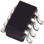
ICGOO电子元器件商城为您提供AD7457BRTZ-REEL7由Analog设计生产,在icgoo商城现货销售,并且可以通过原厂、代理商等渠道进行代购。 AD7457BRTZ-REEL7价格参考¥28.31-¥33.97。AnalogAD7457BRTZ-REEL7封装/规格:数据采集 - 模数转换器, 12 Bit Analog to Digital Converter 1 Input 1 SAR SOT-23-8。您可以下载AD7457BRTZ-REEL7参考资料、Datasheet数据手册功能说明书,资料中有AD7457BRTZ-REEL7 详细功能的应用电路图电压和使用方法及教程。
AD7457BRTZ-REEL7是Analog Devices Inc.生产的一款12位、高速、低功耗逐次逼近型模数转换器(ADC),采用6引脚SOT-23封装,适合对空间和功耗敏感的应用。其典型应用场景包括便携式仪表、电池供电设备、工业控制与监测系统、传感器信号采集以及嵌入式数据采集系统。

该器件具有单电源供电(2.7V至5.25V)、低功耗特性(在3V时功耗仅为1mW左右)和高采样速率(最高可达100ksps),非常适合用于需要长时间运行且依赖电池供电的设备,如手持式测试仪器、远程环境监测装置等。其内置的片上采样保持电路和参考电压简化了外围设计,提升了系统集成度。

AD7457BRTZ-REEL7常用于将温度、压力、光强等传感器输出的模拟信号转换为数字信号,供微控制器或处理器进一步处理。由于其小封装和高可靠性,也广泛应用于空间受限的工业和医疗设备中,如智能变送器、便携式医疗监测仪等。此外,该型号采用卷带包装(REEL7),适用于自动化贴片生产线,适合大规模电子产品制造。
| 参数 | 数值 |
| 产品目录 | 集成电路 (IC)半导体 |
| 描述 | IC ADC 12BIT PSEUDO-DIFF SOT23-8模数转换器 - ADC 12-Bit P/Diff Input 100KSPS |
| 产品分类 | |
| 品牌 | Analog Devices |
| 产品手册 | |
| 产品图片 |
|
| rohs | 符合RoHS无铅 / 符合限制有害物质指令(RoHS)规范要求 |
| 产品系列 | 数据转换器IC,模数转换器 - ADC,Analog Devices AD7457BRTZ-REEL7- |
| 数据手册 | |
| 产品型号 | AD7457BRTZ-REEL7 |
| 产品目录页面 | |
| 产品种类 | 模数转换器 - ADC |
| 位数 | 12 |
| 供应商器件封装 | SOT-23-8 |
| 信噪比 | 71 dB |
| 其它名称 | AD7457BRTZ-REEL7DKR |
| 分辨率 | 12 bit |
| 包装 | Digi-Reel® |
| 商标 | Analog Devices |
| 安装类型 | 表面贴装 |
| 安装风格 | SMD/SMT |
| 封装 | Reel |
| 封装/外壳 | SOT-23-8 |
| 封装/箱体 | SOT-23-8 |
| 工作温度 | -40°C ~ 85°C |
| 工作电源电压 | 5 V |
| 工厂包装数量 | 3000 |
| 接口类型 | Serial (SPI, QSPI, Microwire) |
| 数据接口 | DSP,MICROWIRE™,QSPI™,串行,SPI™ |
| 最大功率耗散 | 3 mW |
| 最大工作温度 | + 85 C |
| 最小工作温度 | - 40 C |
| 标准包装 | 1 |
| 特性 | - |
| 电压参考 | External |
| 电压源 | 单电源 |
| 系列 | AD7457 |
| 结构 | SAR |
| 转换器数 | 1 |
| 转换器数量 | 1 |
| 转换速率 | 100 kS/s |
| 输入数和类型 | 1 个伪差分,双极 |
| 输入类型 | Differential |
| 通道数量 | 1 Channel |
| 采样率(每秒) | 100k |


- 商务部:美国ITC正式对集成电路等产品启动337调查
- 曝三星4nm工艺存在良率问题 高通将骁龙8 Gen1或转产台积电
- 太阳诱电将投资9.5亿元在常州建新厂生产MLCC 预计2023年完工
- 英特尔发布欧洲新工厂建设计划 深化IDM 2.0 战略
- 台积电先进制程称霸业界 有大客户加持明年业绩稳了
- 达到5530亿美元!SIA预计今年全球半导体销售额将创下新高
- 英特尔拟将自动驾驶子公司Mobileye上市 估值或超500亿美元
- 三星加码芯片和SET,合并消费电子和移动部门,撤换高东真等 CEO
- 三星电子宣布重大人事变动 还合并消费电子和移动部门
- 海关总署:前11个月进口集成电路产品价值2.52万亿元 增长14.8%


PDF Datasheet 数据手册内容提取
Low Power, Pseudo Differential, 100 kSPS 12-Bit ADC in an 8-Lead SOT-23 AD7457 FEATURES FUNCTIONAL BLOCK DIAGRAM Specified for VDD of 2.7 V to 5.25 V VDD Low power: 0.9 mW max at 100 kSPS with V = 3 V DD 3 mW max at 100 kSPS with V = 5 V DD Pseudo differential analog input VIN+ 12-BIT Wide input bandwidth: T/H SUCCESSIVE 70 dB SINAD at 30 kHz input frequency VIN– APPROAXDIMCATION Flexible power/serial clock speed management VREF No pipeline delays High speed serial interface—SPI®-/QSPI™-/ MICROWIRE™-/DSP-compatible SCLK Automatic power-down mode SDATA AD7457 CONTROL LOGIC 8-lead SOT-23 package CS APPLICATIONS TBraatntesrdyu-pceorw inetreerdf asycest ems GND 03157-0-013 Data acquisition systems Figure 1. Portable instrumentation GENERAL DESCRIPTION PRODUCT HIGHLIGHTS 1. Operation with 2.7 V to 5.25 V power supplies. The AD7457 is a 12-bit, low power, successive approximation 2. Low power consumption. With a 3 V supply, the AD7457 (SAR) analog-to-digital converter that features a pseudo offers 0.9 mW maximum power consumption for a differential analog input. This part operates from a single 2.7 V 100 kSPS throughput rate. to 5.25 V power supply and features throughput rates of up to 3. Pseudo differential analog input. 100 kSPS. 4. Flexible power/serial clock speed management. The The part contains a low noise, wide bandwidth, differential conversion rate is determined by the serial clock, allowing track-and-hold (T/H) amplifier that can handle input frequen- the power to be reduced as the conversion time is reduced cies in excess of 1 MHz. The reference voltage for the AD7457 is through the serial clock speed increase. Automatic power- applied externally to the V pin and can range from 100 mV to down after conversion allows the average power consump- REF V , depending on what suits the application. tion to be reduced. DD 5. Variable voltage reference input. The conversion process and data acquisition are controlled 6. No pipeline delays. using CS and the serial clock, allowing the device to interface 7. Accurate control of the sampling instant via the CS input with microprocessors or DSPs. The SAR architecture of this and once-off conversion control. part ensures that there are no pipeline delays. 8. ENOB > 10 bits typically with 500 mV reference. The AD7457 uses advanced design techniques to achieve very low power dissipation. Rev. A Information furnished by Analog Devices is believed to be accurate and reliable. However, no responsibility is assumed by Analog Devices for its use, nor for any infringements of patents or other rights of third parties that may result from its use. One Technology Way, P.O. Box 9106, Norwood, MA 02062-9106, U.S.A. Specifications subject to change without notice. No license is granted by implication or otherwise under any patent or patent rights of Analog Devices. Trademarks and Tel: 781.329.4700 www.analog.com registered trademarks are the property of their respective owners. Fax: 781.326.8703 © 2005 Analog Devices, Inc. All rights reserved.
AD7457 TABLE OF CONTENTS Specifications.....................................................................................3 Analog Input...............................................................................12 Timing Specifications.......................................................................5 Analog Input Structure..............................................................12 Absolute Maximum Ratings............................................................6 Digital Inputs..............................................................................13 ESD Caution..................................................................................6 Reference Section.......................................................................13 Pin Configuration and Function Descriptions.............................7 Serial Interface............................................................................13 Typical Performance Characteristics.............................................8 Power Consumption..................................................................14 Terminology....................................................................................10 Microprocessor Interfacing.......................................................14 Theory of Operation......................................................................11 Application Hints...........................................................................16 Circuit Information....................................................................11 Grounding and Layout..............................................................16 Converter Operation..................................................................11 Outline Dimensions.......................................................................17 ADC Transfer Function.............................................................11 Ordering Guide..........................................................................17 Typical Connection Diagram...................................................11 REVISION HISTORY 2/05—Rev. 0 to Rev. A Changes to Table 3............................................................................6 Changes to Ordering Guide..........................................................17 10/03—Rev. 0: Initial Version Rev. A | Page 2 of 20
AD7457 SPECIFICATIONS V = 2.7 V to 5.25 V, f = 10 MHz, f = 100 kSPS, V = 2.5 V, T = T to T , unless otherwise noted. DD SCLK S REF A MIN MAX Table 1. Parameter Test Conditions/Comments B Version1 Unit DYNAMIC PERFORMANCE f = 30 kHz IN Signal to Noise Ratio (SNR)2 71 dB min Signal to (Noise + Distortion) (SINAD)2 70 dB min Total Harmonic Distortion (THD)2 −84 dB typ −75 dB max Peak Harmonic or Spurious Noise2 −86 dB typ −75 dB max Intermodulation Distortion (IMD)2 fa = 25 kHz; fb = 35 kHz Second-Order Terms −80 dB typ Third-Order Terms −80 dB typ Aperture Delay2 5 ns typ Aperture Jitter2 50 ps typ Full-Power Bandwidth2, 3 @ −3 dB 20 MHz typ @ −0.1 dB 2.5 MHz typ DC ACCURACY Resolution 12 Bits Integral Nonlinearity (INL)2 ±1 LSB max Differential Nonlinearity (DNL)2 Guaranteed no missed codes to 12 bits ±0.95 LSB max Offset Error2 ±4.5 LSB max Gain Error2 ±2 LSB max ANALOG INPUT Full-Scale Input Span VIN+ − VIN− VREF V Absolute Input Voltage V V V IN+ REF VIN−4 VDD = 2.7 V to 3.6 V −0.1 to +0.4 V V = 4.75 V to 5.25 V −0.1 to +1.5 V DD DC Leakage Current ±1 µA max Input Capacitance When in track/hold 30/10 pF typ REFERENCE INPUT V Input Voltage5 ±1% tolerance for specified performance 2.5 V REF DC Leakage Current ±1 µA max V Input Capacitance When in track/hold 10/30 pF typ REF LOGIC INPUTS Input High Voltage, V 2.4 V min INH Input Low Voltage, V 0.8 V max INL Input Current, I Typically 10 nA, V = 0 V or V ±1 µA max IN IN DD Input Capacitance, C 6 10 pF max IN LOGIC OUTPUTS Output High Voltage, V V = 4.75 V to 5.25 V, I = 200 µA 2.8 V min OH DD SOURCE V = 2.7 V to 3.6 V, I = 200 µA 2.4 V min DD SOURCE Output Low Voltage, V I = 200 µA 0.4 V max OL SINK Floating-State Leakage Current ±1 µA max Floating-State Output Capacitance6 10 pF max Output Coding Straight natural binary CONVERSION RATE Conversion Time 1.6 µs with a 10 MHz SCLK 16 SCLK cycles Track-and-Hold Acquisition Time2 1 µs max Throughput Rate See the Serial Interface section 100 kSPS max Rev. A | Page 3 of 20
AD7457 Parameter Test Conditions/Comments B Version1 Unit POWER REQUIREMENTS V 2.7/5.25 V min/max DD I 7, 8 DD During Conversion6 V = 4.75 V to 5.25 V 1.5 mA max DD V = 2.7 V to 3.6 V 1.2 mA max DD Normal Mode (Static) SCLK on or off 0.5 mA typ Normal Mode (Operational) V = 4.75 V to 5.25 V 0.7 mA max DD V = 2.7 V to 3.6 V 0.33 mA max DD Power-Down SCLK on or off 1 µA max Power Dissipation Normal Mode (Operational) V = 5 V 3 mW max DD V = 3 V 0.9 mW max DD Power-Down V = 5 V; SCLK on or off 5 µW max DD V = 3 V; SCLK on or off 3 µW max DD 1 Temperature range for B version: −40°C to +85°C. 2 See the Terminology section. 3 Analog inputs with slew rates exceeding 27 V/µs (full-scale input sine wave > 3.5 MHz) within the acquisition time may cause an incorrect result to be returned by the converter. 4 A dc input is applied to VIN– to provide a pseudo ground for VIN+. 5 The AD7457 is functional with a reference input range of 100 mV to VDD. 6 Guaranteed by characterization. 7 See the Power Consumption section. 8 Measured with a full-scale dc input. Rev. A | Page 4 of 20
AD7457 TIMING SPECIFICATIONS1 V = 2.7 V to 5.25 V, f = 10 MHz, f = 100 kSPS, V = 2.5 V, T = T to T , unless otherwise noted. DD SCLK S REF A MIN MAX Table 2. Parameter Limit at T , T Unit Description MIN MAX f 2 10 kHz min SCLK 10 MHz max t 16 × t t = 1/f CONVERT SCLK SCLK SCLK 1.6 µs max t2 10 ns min CS rising edge to SCLK falling edge setup time t33 20 ns max Delay from CS rising edge until SDATA three-state disabled t3 40 ns max Data access time after SCLK falling edge 4 t 0.4 t ns min SCLK high pulse width 5 SCLK t 0.4 t ns min SCLK low pulse width 6 SCLK t 10 ns min SCLK edge to data valid hold time 7 t4 10 ns min SCLK falling edge to SDATA three-state enabled 8 35 ns max SCLK falling edge to SDATA three-state enabled t 5 1 µs max Power-up time from full power-down POWER-UP t 7.4 µs min Minimum time spent in power-down POWER-DOWN 1 The timing specifications are guaranteed by characterization. All input signals are specified with tr = tf = 5 ns (10% to 90% of VDD) and timed from a voltage level of 1.6 V. See Figure 2 and the Serial Interface section. 2 Mark/space ratio for the SCLK input is 40/60 to 60/40. 3 Measured with the load circuit of Figure 3 and defined as the time required for the output to cross 0.8 V or 2.4 V with VDD = 5 V, and the time required for the output to cross 0.4 V or 2.0 V for VDD = 3 V. 4 t8 is derived from the measured time taken by the data outputs to change 0.5 V when loaded with the circuit of Figure 3. The measured number is then extrapolated back to remove the effects of charging or discharging the 25 pF capacitor. This means that the time, t8, quoted in the timing characteristics is the true bus relinquish time of the part and is independent of the bus loading. 5 See the Power Consumption section. POWER CONVERT UP START TRACK HOLD TRACK TPOWERUP TPOWERUP TACQUISITION TACQUISTION CS AUTOMATIC t t5 POWER DOWN SCLK 2 SDATA THREE-STATE 40 LEA0tD3ING0 tZ4ERO0S DB1t16 DB10 t7DB2 DBt18 DB0 TTPHORWEEER-DSOTWATNE 03157-0-001 Figure 2. AD7457 Serial Interface Timing Diagram Rev. A | Page 5 of 20
AD7457 ABSOLUTE MAXIMUM RATINGS T = 25°C, unless otherwise noted. A Table 3. Stresses above those listed under Absolute Maximum Ratings Parameter Rating may cause permanent damage to the device. This is a stress VDD to GND −0.3 V to +7 V rating only; functional operation of the device at these or any VIN+ to GND −0.3 V to VDD + 0.3 V other conditions above those listed in the operational sections VIN– to GND −0.3 V to VDD + 0.3 V of this specification is not implied. Exposure to absolute Digital Input Voltage to GND −0.3 V to +7 V maximum rating conditions for extended periods may affect Digital Output Voltage to GND −0.3 V to VDD + 0.3 V device reliability. VREF to GND −0.3 V to VDD + 0.3 V Input Current to Any Pin Except Supplies1 ±10 mA IOL 1.6mA Operating Temperature Range Commercial (B Version) −40°C to +85°C TO Storage Temperature Range −65°C to +150°C OUTPPUINT CL 1.6V Junction Temperature 150°C 25pF θθJJAC TThheerrmmaall IImmppeeddaannccee 29111.9.59°°CC//WW ((SSOOTT--2233)) 2IO0H0µA 03157-0-012 Lead Temperature, Soldering Vapor Phase (60 sec) 215°C Infrared (15 sec) 220°C Figure 3. Load Circuit for Digital Output Timing Specifications Pb-Free Temperature, Soldering Reflow 260(+0)°C 1 Transient currents of up to 100 mA do not cause SCR latch-up. ESD CAUTION ESD (electrostatic discharge) sensitive device. Electrostatic charges as high as 4000 V readily accumulate on the human body and test equipment and can discharge without detection. Although this product features proprietary ESD protection circuitry, permanent damage may occur on devices subjected to high energy electrostatic discharges. Therefore, proper ESD precautions are recommended to avoid performance degradation or loss of functionality. Rev. A | Page 6 of 20
AD7457 PIN CONFIGURATION AND FUNCTION DESCRIPTIONS VDD 1 8 VREF SCLK 2 AD7457 7 VIN+ SDACTAS 34 (NToOt Pto V SIEcWale) 65 VGINND– 03157-0-002 Figure 4. 8-Lead SOT-23 Pin Configuration Table 4. Pin Function Descriptions Pin No. Mnemonic Description 1 VDD Power Supply Input. VDD is 2.7 V to 5.25 V. This supply should be decoupled to GND with a 0.1 µF capacitor and a 10 µF tantalum capacitor. 2 SCLK Serial Clock. Logic input. SCLK provides the serial clock for accessing data from the part. This clock input is also used as the clock source for the conversion process. 3 SDATA Serial Data. Logic output. The conversion result from the AD7457 is provided on this output as a serial data stream. The bits are clocked out on the falling edge of the SCLK input. The data stream of the AD7457 consists of four leading zeros followed by the 12 bits of conversion data that are provided MSB first. The output coding is straight (natural) binary. 4 CS Chip Select. This input provides the dual function of powering up the device and initiating a conversion on the AD7457. 5 GND Analog Ground. Ground reference point for all circuitry on the AD7457. All analog input signals and any external reference signal should be referred to this GND voltage. 6 VIN– Inverting Input. This pin sets the ground reference point for the VIN+ input. Connect to ground or to a dc offset to provide a pseudo ground. 7 VIN+ Noninverting Analog Input. 8 VREF Reference Input for the AD7457. An external reference in the range 100 mV to VDD must be applied to this input. The specified reference input is 2.5 V. This pin should be decoupled to GND with a capacitor of at least 0.33 µF. Rev. A | Page 7 of 20
AD7457 TYPICAL PERFORMANCE CHARACTERISTICS T = 25°C, f = 100 kSPS, f = 10 MHz, V = 2.7 V to 5.25 V, V = 2.5 V, unless otherwise noted. A S SCLK DD REF 75 1.0 0.8 VDD = 5V 0.6 0.4 B) S dB) VDD = 3V R (L 0.2 SINAD ( 70 L ERRO –0.02 N D –0.4 –0.6 65 03157-0-014 ––01..80 03157-0-017 10 20 30 40 50 0 1024 2048 3072 4096 CODE FREQUENCY (kHz) Figure 5. SINAD vs. Analog Input Frequency for VDD = 3 V and 5 V Figure 8. Typical DNL for the AD7457 for VDD = 5 V 0 1.0 100mV p-p SINEWAVE ON VDD –20 NO DECOUPLING ON VDD 0.8 0.6 –40 0.4 B) PSRR (dB)–1––860000 VDD= 3VVDD= 5V INL ERROR (LS ––000...2420 –0.6 ––112400 03157-0-015 ––01..80 03157-0-018 0 100 200 300 400 500 600 700 800 900 1000 0 1024 2048 3072 4096 CODE SUPPLY RIPPLE FREQUENCY(kHz) Figure 6. PSRR vs. Supply Ripple Frequency Without Supply Decoupling Figure 9. Typical INL for the AD7457 for VDD = 5 V 0 10,000 9949 8192 POINT FFT CODES –20 ffSINA =M P3L0Ek H= z100kSPS 9,000 SINAD = 71dB 8,000 THD =–82dB –40 SFDR =–83dB 7,000 6,000 NR (dB) –60 OUNTS 5,000 S –80 C 4,000 3,000 –100 2,000 ––112400 03157-0-016 1,0000 27 CODES 24 CODES 03157-0-019 0 30 50 100 2046 2047 2048 2049 2050 2051 FREQUENCY (kHz) CODES Figure 7. Dynamic Performance for VDD = 5 V Figure 10. Histogram of 10,000 Conversions of a DC Input Rev. A | Page 8 of 20
AD7457 4.0 12 VDD = 3V 3.5 3.0 B) 11 L (LSB) 22..50 OF BITS (LS 10 VDD = 5V N DN 1.5 BER 9 CHANGE I 10..05 POSITIVE DNL TIVE NUM 8 C 0 FE ––01..50 NEGATIVE DNL 03157-0-020 EF 76 03157-0-022 0 0.5 1.0 1.5 2.0 2.5 3.0 3.5 0 0.5 1.0 1.5 2.0 2.5 3.0 3.5 VREF (V) VREF (V) Figure 11. Changes in DNL vs. VREF for VDD = 5 V Figure 13. ENOB vs. VREF for VDD = 3 V and 5 V 5 4 3 SB) L NL ( 2 N I GE I 1 POSITIVE INL N HA C 0 NEGATIVE INL ––12 03157-0-021 0 0.5 1.0 1.5 2.0 2.5 3.0 3.5 VREF (V) Figure 12. Change in INL vs. VREF for VDD = 5 V Rev. A | Page 9 of 20
AD7457 TERMINOLOGY The calculation of the intermodulation distortion is as per the Signal to (Noise + Distortion) Ratio (SINAD) total harmonic distortion specification, where it is the ratio of The measured ratio of SINAD at the output of the ADC. The the rms sum of the individual distortion products to the rms signal is the rms amplitude of the fundamental. Noise is the amplitude of the sum of the fundamentals expressed in dB. sum of all nonfundamental signals up to half the sampling frequency (f/2), excluding dc. The ratio is dependent on the S Aperture Delay number of quantization levels in the digitization process; the The amount of time from the leading edge of the sampling more levels, the smaller the quantization noise. The theoretical clock until the ADC actually takes the sample. SINAD ratio for an ideal N-bit converter with a sine wave input is given by Aperture Jitter ( ) ( ) The sample-to-sample variation in the effective point in time at Signalto Noise+Distortion = 6.02N +1.76 dB which the actual sample is taken. Therefore, for a 12-bit converter, the SINAD is 74 dB. Full-Power Bandwidth The full-power bandwidth of an ADC is that input frequency Total Harmonic Distortion (THD) at which the amplitude of the reconstructed fundamental is The ratio of the rms sum of harmonics to the fundamental. For reduced by 0.1 dB or 3 dB for a full-scale input. the AD7457, it is defined as Integral Nonlinearity (INL) V2 +V2 +V2 +V2 +V2 THD(dB)=20log 2 3 4 5 6 The maximum deviation from a straight line passing through V the endpoints of the ADC transfer function. 1 where: Differential Nonlinearity (DNL) The difference between the measured and the ideal 1 LSB V is the rms amplitude of the fundamental. 1 change between any two adjacent codes in the ADC. V, V, V, V, and V are the rms amplitudes of the second to the 2 3 4 5 6 Offset Error sixth harmonics. The deviation of the first code transition (000...000 to 000...001) from the ideal (that is, AGND + 1 LSB). Peak Harmonic or Spurious Noise The ratio of the rms value of the next largest component in the Gain Error ADC output spectrum (up to f/2 and excluding dc) to the rms S The deviation of the last code transition (111...110 to 111...111) value of the fundamental. Normally, the value of this specifica- from the ideal (that is, V − 1 LSB), after the offset error has REF tion is determined by the largest harmonic in the spectrum, but, been adjusted out. for ADCs where the harmonics are buried in the noise floor, it is a noise peak. Track-and-Hold Acquisition Time The minimum time required for the track-and-hold amplifier to Intermodulation Distortion remain in track mode for its output to reach and settle to within With inputs consisting of sine waves at two frequencies, fa and 0.5 LSB of the applied input signal. fb, any active device with nonlinearities creates distortion prod- ucts at sum and difference frequencies of mfa ± nfb, where m, n Power Supply Rejection Ratio (PSRR) = 0, 1, 2, 3, and so on. Intermodulation distortion terms are The ratio of the power in the ADC output at full-scale those for which neither m nor n are equal to zero. For example, frequency, f, to the power of a 100 mV p-p sine wave applied to the second order terms include (fa + fb) and (fa − fb), while the the ADC V supply of frequency fs. The frequency of this DD third order terms include (2fa + fb), (2fa − fb), (fa + 2fb) and input varies from 1 kHz to 1 MHz. (fa − 2fb). PSRR(dB) = 10 log(Pf/Pfs) The AD7457 is tested using the CCIF standard, where two input Pf is the power at frequency f in the ADC output; Pfs is the frequencies near the top end of the input bandwidth are used. power at frequency fs in the ADC output. In this case, the second order terms are usually distanced in fre- quency from the original sine waves, while the third order terms are usually at a frequency close to the input frequencies. As a result, the second and third order terms are specified separately. Rev. A | Page 10 of 20
AD7457 THEORY OF OPERATION CIRCUIT INFORMATION CAPACITIVE DAC The AD7457 is a 12-bit, low power, single supply, successive B CS approximation analog-to-digital converter (ADC) with a VIN+ pseudo differential analog input. It operates with a single 2.7 V VIN– AA SSWW21 SW3 COLONTGRICOL t1Vo0R 05EF .k 2pS5iP nVS. .p Iot wreeqru siurepsp alyn aenxdte irsn caal praebfelree onfc teh troo ubge happuptl ireadt etso uthpe t o B VREF CS COMPARATOR CAPDAACCITIVE 03157-0-004 Figure 15. ADC Conversion Phase The AD7457 has an on-chip differential track-and-hold amplifier, a successive approximation (SAR) ADC, and a serial ADC TRANSFER FUNCTION interface housed in an 8-lead SOT-23 package. The serial clock input accesses data from the part and provides the clock source The output coding for the AD7457 is straight (natural) binary. for the successive approximation ADC. The AD7457 automati- The designed code transitions occur at successive LSB values cally powers down after conversion, resulting in low power (1 LSB, 2 LSB, and so on). The LSB size is V /4096. The ideal REF consumption. transfer characteristics of the AD7457 are shown in Figure 16. CONVERTER OPERATION 1LSB = VREF/4096 The AD7457 is a successive approximation ADC based around 111...11 two capacitive DACs. Figure 14 and Figure 15 show simplified 111...10 schematics of the ADC in the acquisition phase and the conver- E sion phase, respectively. The ADC is comprised of control logic, OD 111...00 C a SAR, and two capacitive DACs. In Figure 14 (acquisition DC 011...11 A pccoahpmaaspceia)t,ro SartW oarr3 ri asisy h sce lalodcsq eiundi ,r aSe bW tahl1ea nadncifedfde S rcWeonn2tid aailrt iesoi ignnn, aaPnlo odsin tti htohen es Aainm, ptphuleti. n g 000000000.........001010 03157-0-005 0V1LSB VREF–1LSB ANALOG INPUT CAPACITIVE DAC Figure 16. Ideal Transfer Characteristics B CS VIN+ TYPICAL CONNECTION DIAGRAM A SW1 SW3 CONTROL VIN– A SW2 LOGIC Figure 17 shows a typical connection diagram for the AD7457. B VREF CS COMPARATOR CAPDAACCITIVE 03157-0-003 Ipan l2a t.n5he iV so sfde tethuceop u,s typhslteeed Gm rN.e TfDehr epen iVncR eiE sFs ocpouinnrc niese. ccTtoehnden tseoicg ttnehadel atsono uathlrocege A gisDr o7u8n0d, Figure 14. ADC Acquisition Phase connected to the V analog input via a unity gain buffer. A IN+ When the ADC starts a conversion (Figure 15), SW3 opens, and dc voltage is connected to the VIN– pin to provide a pseudo SW1 and SW2 move to Position B, causing the comparator to ground for the VIN+ input. The VDD pin should be decoupled to become unbalanced. Both inputs are disconnected once the AGND with a 10 µF tantalum capacitor in parallel with a 0.1 µF conversion begins. The control logic and the charge redistribu- ceramic capacitor. The reference pin should be decoupled to tion DACs are used to add and subtract fixed amounts of charge AGND with a capacitor of at least 0.33 µF. The conversion result from the sampling capacitor arrays to bring the comparator is output in a 16-bit word with four leading zeros followed by back into a balanced condition. When the comparator is rebal- the MSB of the 12-bit result. anced, the conversion is complete. The control logic generates the ADC’s output code. The output impedances of the sources driving the V and the V pins must be matched; otherwise IN+ IN– the two inputs have different settling times, resulting in errors. Rev. A | Page 11 of 20
AD7457 +2.7V TO +5.25V ANALOG INPUT STRUCTURE SUPPLY 0.1µF 10µF Figure 19 shows the equivalent circuit of the analog input SERIAL VDD INTERFACE structure of the AD7457. The four diodes provide ESD protec- VREF AD7457 tion for the analog inputs. Care must be taken to ensure that the P-TO-P VIN+ SCLK analog input signals never exceed the supply rails by more than SDATA µC/µP 300 mV, which causes these diodes to become forward biased CS and start conducting into the substrate. These diodes can con- VIN– DC INPUT GND duct up to 10 mA without causing irreversible damage to the VOLTAGE VREF part. Typically, the C1 capacitors in Figure 19 are 4 pF and can 2.5V 0.33µF AD780 03157-0-006 bluem aptterdib cuotemdp pornimenatrsi lmy atod ep iunp c oafp tahceit oannc ree. sTishtaen rcees iostfo trhse a re switches. The value of these resistors is typically about 100 Ω. Figure 17. Typical Connection Diagram The capacitors, C2, are the ADC’s sampling capacitors, which ANALOG INPUT typically have a capacitance of 16 pF. The AD7457 has a pseudo differential analog input. The V IN+ For ac applications, removing high frequency components from input is coupled to the signal source and should have an ampli- the analog input signal through the use of an RC low pass filter tude of V p-p to make use of the full dynamic range of the REF on the relevant analog input pins is recommended. In applica- part. A dc input is applied to the V . The voltage applied to this IN− tions where harmonic distortion and the signal-to-noise ratio input provides an offset from ground or a pseudo ground for are critical, the analog input should be driven from a low the V input. Ensure that (V + V ) is less than or equal to IN+ IN− IN+ impedance source. Large source impedances can significantly V to avoid exceeding the maximum ratings of the ADC. The DD affect the ac performance of the ADC, which may necessitate main benefit of pseudo differential inputs is that they separate the use of an input buffer amplifier. The choice of the op amp is the analog input signal ground from the ADC’s ground, allow- a function of the particular application. ing dc common-mode voltages to be canceled. VDD Because the ADC operates from a single supply, it is necessary to level shift ground-based bipolar signals to comply with the input requirements. An op amp (for example, the AD8021) can D R1 C2 be configured to rescale and level shift a ground-based (bipolar) VIN+ signal, so that it is compatible with the input range of the C1 D AD7457. See Figure 18. When a conversion takes place, the pseudo ground corresponds to 0 and the maximum analog input corresponds to 4096. VDD 2.5V R 1.25V D R1 C2 +1.25V R 0V VIN– –1.205VV VIN 3R VIN+ C1 D R VIN–AD7457VREF 03157-0-008 0.33µF Figure 19. Equivalent Analog Input Circuit (Conversion Phase, Switches Open; Track Phase, Switches Closed) EVXRETFER(2N.5AVL) 03157-0-007 Wsouhrecne nimo pamedpalnifciee rs hiso uusledd b teo l idmriivtee dt htoe alonwal ovgal iunepsu. Tt, hthe em axi- Figure 18. Op Amp Configuration to Level Shift a Bipolar Input Signal mum source impedance depends on the amount of total harmonic distortion that can be tolerated. The THD increases as the source impedance increases and performance degrades. Figure 20 shows a graph of the THD vs. analog input signal frequency for different source impedances. Rev. A | Page 12 of 20
AD7457 –50 0.33 µF should be placed on the V pin. Suitable reference TA = 25°C REF sources for the AD7457 include the AD780 and the ADR421. –60 Figure 22 shows a typical connection diagram for the VREF pin. VDD –70 200Ω B) AD780 AD74571 d THD (–80 100Ω NC 1 OPSEL 8 NC VREF VDD 2 VIN 7 NC 2.5V 3 TEMP VOUT 6 –90 0.1µF 10µF 0.1µF 4 GND TRIM 5 NC 0.33µF 10Ω 62Ω 10 20 30 40 5003157-0-009 1ADDITIONAL PINS OMITTED FOR CLNACR =IT NYO. CONNECT 03157-0-011 INPUT FREQUENCY (kHz) Figure 22. Typical VREF Connection Diagram for VDD = 5 V Figure 20. THD vs. Analog Input Frequency for Various Source Impedances SERIAL INTERFACE Figure 21 shows a graph of THD vs. analog input frequency for Figure 2 shows a detailed timing diagram of the serial interface various supply voltages, while sampling at 100 kSPS with an of the AD7457. The serial clock provides the conversion clock SCLK of 10 MHz. In this case, the source impedance is 10 Ω. and also controls the transfer of data from the device during –50 conversions. TA = 25°C –55 The falling edge of CS powers up the AD7457 and also puts the track-and-hold into track. Power-up time is 1 µs minimum and, –60 in this time, the device also acquires the analog input signal. CS –65 must remain low for the duration of power-up. The rising edge B) D (d–70 of CS initiates the conversion process, puts the track-and-hold TH into hold mode, and takes the serial data bus out of three-state. –75 VDD= 2.7V The conversion requires 16 SCLK cycles to complete. VDD= 3.6V –80 VDD= 4.75V On the sixteenth SCLK falling edge, after the time t8, the serial ––9805 VDD= 5.25V 03157-0-010 denattear bs ufus lgl opeosw bearc-kd oinwton .t Ihtr reeem-sataintes ainn dp othwee rd-edvoicwen a uutnotmil tahtiec ally 10 20 30 40 50 next falling edge of CS. For specified performance, the through- INPUT FREQUENCY (kHz) put rate should not exceed 100 kSPS, which means that there Figure 21. THD vs. Analog Input Frequency for Various Supply Voltages should be no less than 10 µs between consecutive CS falling edges. DIGITAL INPUTS The conversion result from the AD7457 is provided on the The digital inputs applied to the AD7457 are not limited by the SDATA output as a serial data stream. The bits are clocked out maximum ratings that limit the analog inputs. Instead, the digital on the falling edge of the SCLK input. The data stream of the inputs applied, that is, CS and SCLK, can go to 7 V and are not AD7457 consists of four leading zeros, followed by the 12 bits of restricted by the V + 0.3 V limits as on the analog input. DD conversion data that are provided MSB first. The output coding The main advantage of the inputs not being restricted to the is straight (natural) binary. V + 0.3 V limit is that power supply sequencing issues are DD Sixteen serial clock cycles are, therefore, required to perform a avoided. If CS or SCLK are applied before V , there is no risk DD conversion and to access data from the AD7457. A rising edge of latch-up as there would be on the analog inputs if a signal of CS provides the first leading zero to be read in by the micro- greater than 0.3 V were applied prior to V . DD controller or DSP. The remaining data is then clocked out on REFERENCE SECTION the subsequent SCLK falling edges, beginning with the second leading zero. Thus, the first falling clock edge on the serial clock An external source is required to supply the reference to the after CS has gone high provides the second leading zero. The AD7457. This reference input can range from 100 mV to V . DD final bit in the data transfer, before the device goes into power- The specified reference is 2.50 V for the power supply range down, is valid on the sixteenth falling edge of SCLK, having 2.70 V to 5.25 V. Errors in the reference source result in gain been clocked out on the previous (fifteenth) falling edge. errors in the AD7457 transfer function. A capacitor of at least Rev. A | Page 13 of 20
AD7457 In applications with a slow SCLK, it is possible to read in data 2.5 TA = 25°C on each SCLK rising edge. In this case, the first falling edge of SCLK after the CS rising edge clocks out the second leading 2.0 zero and can be read in on the following rising edge. If the first SCLK edge after the CS rising edge is a falling edge, the first W)1.5 leading zero that was clocked out when CS went high is missed, m R ( VDD = 5V unless it was not read on the first SCLK falling edge. The fif- WE O1.0 teenth falling edge of SCLK clocks out the last bit of data, which P can be read in by the following rising SCLK edge. 0.5 POWER CONSUMPTION The AD7457 automatically enters power-down at the end of 0 VDD = 3V 03157-0-024 each conversion. When in the power-down mode, all analog 0 20 40 60 80 100 THROUGHPUT (kSPS) circuitry is powered down and the current consumption is 1 µA. To achieve the specified power consumption (which is the Figure 24. Power vs. Throughput Rate for SCLK = 10 MHz for VDD = 3 V and 5 V lowest), there are a few things the user should keep in mind. MICROPROCESSOR INTERFACING The serial interface of the AD7457 allows the part to be con- The conversion time of the device is determined by the serial nected to a range of different microprocessors. This section clock frequency. The faster the SCLK frequency, the shorter the explains how to interface the AD7457 with the ADSP-218x conversion time. Therefore, as the clock frequency used is serial interface. increased, the ADC is dissipating power for a shorter period of time (during conversion) and it remains in power-down for a AD7457 to ADSP-218x longer percentage of the cycle time or throughput rate. This The ADSP-218x family of DSPs can be interfaced directly to the can be seen in Figure 23, which shows typical I vs. SCLK DD AD7457 without any glue logic. The serial clock for the ADC is frequency for V of 3 V and 5 V, when operating the device at DD provided by the DSP. SDATA from the ADC is connected to the the maximum throughput of 100 kSPS. data receive (DR) input of the serial port and CS can be con- 2.5 trolled by a flag (FL0). The connection diagram is shown in TA = 25°C Figure 25. 2.0 AD74571 ADSP-21xx1 SCLK SCLK SPORT0 1.5 A) SDATA DR0 m I (DD1.0 RFS VDD = 5V CS FL0 SPORT1 VDD = 3V 0.50 03157-0-023 1ADDITIONAL PINS OMITTED FOR CLARITY. 03157-0-025 0 2 4 6 8 10 Figure 25. AD7457 to ADSP-218x SCLK Frequency (MHz) SPORT0 must be enabled to receive the conversion data and to Figure 23. IDD vs. SCLK Frequency for VDD = 3 V and 5 V provide the SCLK, while SPORT1 must be configured for flags when Operating at 100 kSPS and so on. Figure 24 shows typical power consumption vs. throughput rate for the maximum SCLK frequency of 10 MHz. In this case, the conversion time is the same for all throughputs, because the SCLK frequency is fixed. As the throughput rate decreases, the average power consumption decreases, because the ADC spends more time in power-down. Rev. A | Page 14 of 20
AD7457 Table 5. SPORT0 Configuration SPORT0 is configured by setting the bits in its control register, Bit Setting Comment/Description as listed in Table 5. ISCLK 1 Serial clock is generated internally SLEN 1111 16 bits of conversion data The flag to generate the CS signal is generated by SPORT1. It is RFSR 0 Receive frame sync required every word connected to both the ADC and the RFS input of SPORT0 to TFSR Don’t care Not used provide the frame sync signal for the DSP. IRFS 0 RFS is set to be an input and is generated externally. ITFS Don’t care Not used RFSW 1 Alternate receive framing TFSW Don’t care Not used INVRFS 0 RFS is active high INVTFS Don’t care Not used Rev. A | Page 15 of 20
AD7457 APPLICATION HINTS GROUNDING AND LAYOUT of glitches on the power supply line. Fast switching signals, such as clocks, should be shielded with digital ground to avoid The printed circuit board that houses the AD7457 should be radiating noise to other sections of the board, and clock signals designed so that the analog and digital sections are separated should never run near the analog inputs. Avoid crossover of and confined to certain areas of the board. This facilitates the digital and analog signals. Traces on opposite sides of the board use of ground planes that can be easily separated. A minimum should run at right angles to each other. This reduces the effects etch technique is generally best for ground planes, because it of feed through the board. A micro strip technique is the best, gives the best shielding. Digital and analog ground planes but is not always possible with a double-sided board. should be joined in only one place, and the connection should be a star ground point established as close as possible to the In this technique, the component side of the board is dedicated GND pin on the AD7457. to ground planes, while signals are placed on the solder side. Good decoupling is also important. All analog supplies should Avoid running digital lines under the device, because this be decoupled with 10 µF tantalum capacitors in parallel with couples noise onto the die. The analog ground plane should be 0.1 µF capacitors to GND. To achieve the best from these allowed to run under the AD7457 to avoid noise coupling. The decoupling components, place them as close as possible to power supply lines to the AD7457 should use as large a trace as the device. possible to provide low impedance paths and reduce the effects Rev. A | Page 16 of 20
AD7457 OUTLINE DIMENSIONS 2.90 BSC 8 7 6 5 1.60 BSC 2.80 BSC 1 2 3 4 PIN1 INDICATOR 0.65 BSC 1.95 1.30 BSC 1.15 0.90 1.45 MAX 0.22 0.08 0.60 0.15 MAX 00..3282 SEATING 84°° 00..4350 PLANE 0° COMPLIANT TO JEDEC STANDARDS MO-178BA Figure 26. 8-Lead Small Outline Transistor Package [SOT-23] (RT-8) Dimensions shown in millimeters ORDERING GUIDE Model Temperature Range Linearity Error (LSB)1 Package Description Package Option Branding AD7457BRT-R2 –40°C to +85°C ±1 8-Lead SOT-23 RT-8 COJ AD7457BRT-REEL7 –40°C to +85°C ±1 8-Lead SOT-23 RT-8 COJ AD7457BRTZ-REEL72 –40°C to +85°C ±1 8-Lead SOT-23 RT-8 COD 1 Linearity error here refers to integral nonlinearity error. 2 Z = Pb-free part. Rev. A | Page 17 of 20
AD7457 NOTES Rev. A | Page 18 of 20
AD7457 NOTES Rev. A | Page 19 of 20
AD7457 NOTES © 2005 Analog Devices, Inc. All rights reserved. Trademarks and registered trademarks are the property of their respective owners. C03157–0–2/05(A) Rev. A | Page 20 of 20