ICGOO在线商城 > 集成电路(IC) > 线性 - 放大器 - 仪表,运算放大器,缓冲器放大器 > AD8652ARZ
 Datasheet下载
- 型号: AD8652ARZ
- 制造商: Analog
- 库位|库存: xxxx|xxxx
- 要求:
| 数量阶梯 | 香港交货 | 国内含税 |
| +xxxx | $xxxx | ¥xxxx |
查看当月历史价格
查看今年历史价格
AD8652ARZ产品简介:
ICGOO电子元器件商城为您提供AD8652ARZ由Analog设计生产,在icgoo商城现货销售,并且可以通过原厂、代理商等渠道进行代购。 AD8652ARZ价格参考。AnalogAD8652ARZ封装/规格:线性 - 放大器 - 仪表,运算放大器,缓冲器放大器, 电压反馈 放大器 2 电路 满摆幅 8-SOIC。您可以下载AD8652ARZ参考资料、Datasheet数据手册功能说明书,资料中有AD8652ARZ 详细功能的应用电路图电压和使用方法及教程。
AD8652ARZ是由Analog Devices Inc.(亚德诺半导体公司)生产的一款高性能双通道运算放大器,广泛应用于精密信号处理领域。该器件具有低噪声、低偏置电流和高输入阻抗等特性,适用于多种应用场景。

1. 工业自动化与控制:AD8652ARZ的高精度和稳定性使其成为工业控制系统中传感器信号调理的理想选择。它可以用于温度、压力、位移等传感器的信号放大和处理,确保数据采集系统的准确性和可靠性。

2. 医疗设备:在医疗电子设备中,如心电图机、血压计和其他生理信号监测设备,AD8652ARZ可以提供低噪声和高增益性能,确保微弱生物电信号的精确放大和传输,从而提高诊断的准确性。

3. 通信系统:AD8652ARZ的低失真和宽带宽特性使其适合用于通信设备中的信号调理和放大。它可以在无线通信基站、光纤通信模块等应用中发挥重要作用,保证信号的高质量传输。

4. 音频处理:由于其低噪声和低失真特性,AD8652ARZ也常用于音频设备中,如专业音响设备、麦克风前置放大器等,能够有效提升音质,减少背景噪音。

5. 测试与测量仪器:在精密测试仪器中,如示波器、频谱分析仪等,AD8652ARZ可以作为前端放大器,提供稳定的信号放大功能,确保测量结果的准确性。

总之,AD8652ARZ凭借其卓越的性能,在需要高精度、低噪声和稳定性的应用场合中表现出色,广泛应用于工业、医疗、通信、音频和测试测量等多个领域。
| 参数 | 数值 |
| -3db带宽 | - |
| 产品目录 | 集成电路 (IC)半导体 |
| 描述 | IC OPAMP VFB 50MHZ RRO 8SOIC精密放大器 50MHz Low Distort Low Noise CMOS Prec |
| 产品分类 | Linear - Amplifiers - Instrumentation, OP Amps, Buffer Amps集成电路 - IC |
| 品牌 | Analog Devices Inc |
| 产品手册 | |
| 产品图片 |
|
| rohs | 符合RoHS无铅 / 符合限制有害物质指令(RoHS)规范要求 |
| 产品系列 | 放大器 IC,精密放大器,Analog Devices AD8652ARZDigiTrim® |
| 数据手册 | |
| 产品型号 | AD8652ARZ |
| 产品培训模块 | http://www.digikey.cn/PTM/IndividualPTM.page?site=cn&lang=zhs&ptm=30008http://www.digikey.cn/PTM/IndividualPTM.page?site=cn&lang=zhs&ptm=26202 |
| 产品目录页面 | |
| 产品种类 | 精密放大器 |
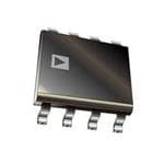
| 供应商器件封装 | 8-SOIC |
| 共模抑制比—最小值 | 100 dB |
| 关闭 | No |
| 包装 | 管件 |
| 压摆率 | 41 V/µs |
| 可用增益调整 | 115 dB |
| 商标 | Analog Devices |
| 增益带宽生成 | 50 MHz |
| 增益带宽积 | 50MHz |
| 安装类型 | 表面贴装 |
| 安装风格 | SMD/SMT |
| 封装 | Tube |
| 封装/外壳 | 8-SOIC(0.154",3.90mm 宽) |
| 封装/箱体 | SOIC-8 |
| 工作温度 | -40°C ~ 125°C |
| 工作电源电压 | 2.7 V to 5.5 V |
| 工厂包装数量 | 98 |
| 放大器类型 | 电压反馈 |
| 最大工作温度 | + 125 C |
| 最小工作温度 | - 40 C |
| 标准包装 | 98 |
| 电压-电源,单/双 (±) | 2.7 V ~ 5.5 V, ±1.35 V ~ 2.75 V |
| 电压-输入失调 | 90µV |
| 电压增益dB | 115 dB |
| 电流-电源 | 17.5mA |
| 电流-输入偏置 | 1pA |
| 电流-输出/通道 | 40mA |
| 电源电压-最大 | 5.5 V |
| 电源电压-最小 | 2.7 V |
| 电源电流 | 17.5 mA |
| 电源类型 | Single |
| 电路数 | 2 |
| 系列 | AD8652 |
| 视频文件 | http://www.digikey.cn/classic/video.aspx?PlayerID=1364138032001&width=640&height=505&videoID=2245193153001http://www.digikey.cn/classic/video.aspx?PlayerID=1364138032001&width=640&height=505&videoID=2245193159001 |
| 转换速度 | 41 V/us |
| 输入偏压电流—最大 | 600 pA |
| 输入电压范围—最大 | 5.1 V |
| 输入补偿电压 | 0.4 mV |
| 输出电流 | 40 mA |
| 输出类型 | 满摆幅 |
| 通道数量 | 2 Channel |


PDF Datasheet 数据手册内容提取
50 MHz, Precision, Low Distortion, Low Noise CMOS Amplifiers Data Sheet AD8651/AD8652 FEATURES PIN CONFIGURATIONS Bandwidth: 50 MHz at 5 V Low noise: 4.5 nV/√Hz Ofefsnetti rveo cltoamgme: o1n0-0m μoVd tey rpaincagle, specified over –NICN 12 AD8651 87 NV+C O–UINT AA 12 AD8652 87 VO+UT B SRInlaepiwlu-tt ro ba-tiraeas:i l 4c i1un rpVrue/μnt sat : n 1d p oAu tput swing +VIN– 34NC( N=T oNOtO Pto CV SOIEcNWaNleE)CT65 ONCUT 03301-001 +INV A– 34 (NToOt Pto V SIEcWale) 65 –+IINN BB 03301-003 Figure 1. 8-Lead MSOP (RM-8) Figure 2. 8-Lead MSOP (RM-8) Single-supply operation: 2.7 V to 5.5 V Space-saving MSOP and SOIC_N packaging NC 1 8 NC APPLICATIONS +–IINN 23 ATODP8 V6IE5W1 76 VO+UT O–UINT AA 12 AD8652 78 VO+UT B OLapsteicr aslo cuormcem durinviecrast/icoonnst rollers V– N4C (=N oNtO to C SOcNaNleE)CT5 NC 03301-002 +INV A– 34 (NToOt Pto V SIEcWale) 65 –+IINN BB 03301-004 Figure 3. 8-Lead SOIC_N (R-8) Figure 4. 8-Lead SOIC_N (R-8) Broadband communications High speed ADCs and DACs Microwave link interface Cell phone PA control Video line drivers Audio GENERAL DESCRIPTION The AD865x family features the newest generation of DigiTrim® in-package trimming. This new generation measures and corrects The AD865x family consists of high precision, low noise, low the offset over the entire input common-mode range, providing distortion, rail-to-rail CMOS operational amplifiers that run less distortion from V variation than is typical of other rail-to- from a single-supply voltage of 2.7 V to 5.5 V. OS rail amplifiers. Offset voltage and CMRR are both specified and The AD865x family is made up of rail-to-rail input and output guaranteed over the entire common-mode range as well as over amplifiers with a gain bandwidth of 50 MHz and a typical the extended industrial temperature range. voltage offset of 100 μV across common mode from a 5 V The AD865x family is offered in the narrow 8-lead SOIC supply. It also features low noise—4.5 nV/√Hz. package and the 8-lead MSOP package. The amplifiers are The AD865x family can be used in communications applications, specified over the extended industrial temperature range such as cell phone transmission power control, fiber optic (−40°C to +125°C). networking, wireless networking, and video line drivers. Rev. D Document Feedback Information furnished by Analog Devices is believed to be accurate and reliable. However, no responsibility is assumed by Analog Devices for its use, nor for any infringements of patents or other One Technology Way, P.O. Box 9106, Norwood, MA 02062-9106, U.S.A. rights of third parties that may result from its use. Specifications subject to change without notice. No license is granted by implication or otherwise under any patent or patent rights of Analog Devices. Tel: 781.329.4700 ©2006–2014 Analog Devices, Inc. All rights reserved. Trademarks and registered trademarks are the property of their respective owners. Technical Support www.analog.com
AD8651/AD8652 Data Sheet TABLE OF CONTENTS Features .............................................................................................. 1 Thermal Resistance .......................................................................5 Applications ....................................................................................... 1 Typical Performance Characteristics ..............................................6 Pin Configurations ........................................................................... 1 Applications ..................................................................................... 14 General Description ......................................................................... 1 Theory of Operation .................................................................. 14 Revision History ............................................................................... 2 Layout, Grounding, and Bypassing Considerations .............. 15 Specifications ..................................................................................... 3 Outline Dimensions ....................................................................... 18 Electrical Characteristics ............................................................. 3 Ordering Guide .......................................................................... 19 Absolute Maximum Ratings ............................................................ 5 ESD Caution .................................................................................. 5 REVISION HISTORY 2/14—Rev. C to Rev. D 6/04—Rev. 0 to Rev. A Change to Figure 18 ............................................................................. 8 Changes to Figure 21 ........................................................................ 8 Change to Figure 21 ............................................................................. 9 Updated Outline Dimensions ....................................................... 18 Change to Figure 29 ............................................................................. 10 Changes to Ordering Guide .......................................................... 19 Change to Figure 30 ............................................................................. 10 8/06—Rev. B. to Rev. C Change to Figure 43 ............................................................................. 12 Changes to Figure 1 to Figure 4 ...................................................... 1 Change to Figure 44 ............................................................................. 12 Changes to Figure 7 and Figure 9 ................................................... 6 Change to Figure 47 ............................................................................. 13 Changes to Figure 23 ........................................................................ 9 Change to Figure 57 ............................................................................. 17 Changes to Figure 53 ...................................................................... 14 Updated Outline Dimensions ....................................................... 18 10/03 Revision 0: Initial Version Changes to Ordering Guide .......................................................... 19 9/04—Rev. A to Rev. B Added AD8652 .................................................................... Universal Change to General Description ....................................................... 1 Changes to Electrical Characteristics ............................................. 3 Changes to Absolute Maximum Ratings ........................................ 5 Change to Figure 23 .......................................................................... 9 Change to Figure 26 .......................................................................... 9 Change to Figure 36 ........................................................................ 11 Change to Figure 42 ........................................................................ 12 Change to Figure 49 ........................................................................ 13 Change to Figure 51 ........................................................................ 13 Inserted Figure 52 ............................................................................ 13 Change to Theory of Operation section ....................................... 14 Change to Input Protection section .............................................. 15 Changes to Ordering Guide ........................................................... 20 Rev. D | Page 2 of 20
Data Sheet AD8651/AD8652 SPECIFICATIONS ELECTRICAL CHARACTERISTICS V+ = 2.7 V, V– = 0 V, V = V+/2, T = 25°C, unless otherwise specified. CM A Table 1. Parameter Symbol Conditions Min Typ Max Unit INPUT CHARACTERISTICS Offset Voltage VOS AD8651 0 V ≤ VCM ≤ 2.7 V 100 350 μV –40°C ≤ TA ≤ +85°C, 0 V ≤ VCM ≤ 2.7 V 1.4 mV –40°C ≤ TA ≤ +125°C, 0 V ≤ VCM ≤ 2.7 V 1.6 mV AD8652 0 V ≤ VCM ≤ 2.7 V 90 300 μV –40°C ≤ TA ≤ +125°C, 0 V ≤ VCM ≤ 2.7 V 0.4 1.3 mV Offset Voltage Drift TCVOS 4 μV/°C Input Bias Current IB 1 10 pA –40°C ≤ TA ≤ +125°C 600 pA Input Offset Current IOS 1 10 pA –40°C ≤ TA ≤ +85°C 30 pA –40°C ≤ TA ≤ +125°C 600 pA Input Voltage Range VCM –0.1 +2.8 V Common-Mode Rejection Ratio CMRR AD8651 V+ = 2.7 V, –0.1 V < VCM < +2.8 V 75 95 dB –40°C ≤ TA ≤ +85°C, –0.1 V < VCM < +2.8 V 70 88 dB –40°C ≤ TA ≤ +125°C, –0.1 V < VCM < +2.8 V 65 85 dB AD8652 V+ = 2.7 V, –0.1 V < VCM < +2.8 V 77 95 dB –40°C ≤ TA ≤ +125°C, –0.1 V < VCM < +2.8 V 73 90 dB Large Signal Voltage Gain AVO RL = 1 kΩ, 200 mV < VO < 2.5 V 100 115 dB RL = 1 kΩ, 200 mV < VO < 2.5 V, TA = 85°C 100 114 dB RL = 1 kΩ, 200 mV < VO < 2.5 V, TA = 125°C 95 108 dB OUTPUT CHARACTERISTICS Output Voltage High VOH IL = 250 μA, –40°C ≤ TA ≤ +125°C 2.67 V Output Voltage Low VOL IL = 250 μA, –40°C ≤ TA ≤ +125°C 30 mV Short-Circuit Limit ISC Sourcing 80 mA Sinking 80 mA Output Current IO 40 mA POWER SUPPLY Power Supply Rejection Ratio PSRR VS = 2.7 V to 5.5 V, VCM = 0 V 76 94 dB –40°C ≤ TA ≤ +125°C 74 93 dB Supply Current ISY AD8651 IO = 0 9 12 mA –40°C ≤ TA ≤ +125°C 14.5 mA AD8652 IO = 0 17.5 19.5 mA –40°C ≤ TA ≤ +125°C 22.5 mA INPUT CAPACITANCE CIN Differential 6 pF Common Mode 9 pF DYNAMIC PERFORMANCE Slew Rate SR G = 1, RL = 10 kΩ 41 V/μs Gain Bandwidth Product GBP G = 1 50 MHz Settling Time, 0.01% G = ±1, 2 V step 0.2 μs Overload Recovery Time VIN × G = 1.48 V+ 0.1 μs Total Harmonic Distortion + Noise THD + N G = 1, RL = 600 Ω, f = 1 kHz, VIN = 2 V p-p 0.0006 % NOISE PERFORMANCE Voltage Noise Density en f = 10 kHz 5 nV/√Hz f = 100 kHz 4.5 nV/√Hz Current Noise Density in f = 10 kHz 4 fA/√Hz Rev. D | Page 3 of 20
AD8651/AD8652 Data Sheet V+ = 5 V, V– = 0 V, V = V+/2, T = 25°C, unless otherwise specified. CM A Table 2. Parameter Symbol Conditions Min Typ Max Unit INPUT CHARACTERISTICS Offset Voltage VOS AD8651 0 V ≤ VCM ≤ 5 V 100 350 μV –40°C ≤ TA ≤ +85°C, 0 V ≤ VCM ≤ 5 V 1.4 mV –40°C ≤ TA ≤ +125°C, 0 V ≤ VCM ≤ 5 V 1.7 mV AD8652 0 V ≤ VCM ≤ 5 V 90 300 μV –40°C ≤ TA ≤ +125°C, 0 V ≤ VCM ≤ 5 V 0.4 1.4 mV Offset Voltage Drift TCVOS 4 μV/°C Input Bias Current IB 1 10 pA –40°C ≤ TA ≤ +85°C 30 pA –40°C ≤ TA ≤ +125°C 600 pA Input Offset Current IOS 1 10 pA –40°C ≤ TA ≤ +85°C 30 pA –40°C ≤ TA ≤ +125°C 600 pA Input Voltage Range VCM –0.1 +5.1 V Common-Mode Rejection Ratio CMRR AD8651 0.1 V < VCM < 5.1 V 80 95 dB –40°C ≤ TA ≤ +85°C, 0.1 V < VCM < 5.1 V 75 94 dB –40°C ≤ TA ≤ +125°C, 0.1 V < VCM < 5.1 V 70 90 dB AD8652 0.1 V < VCM < 5.1 V 84 100 dB –40°C ≤ TA ≤ +125°C, 0.1 V < VCM < 5.1 V 76 95 dB Large Signal Voltage Gain AVO RL = 1 kΩ, 200 mV < VO < 4.8 V 100 115 dB RL = 1 kΩ, 200 mV < VO < 4.8 V, TA = 85°C 98 114 dB RL = 1 kΩ, 200 mV < VO < 4.8 V, TA = 125°C 95 111 dB OUTPUT CHARACTERISTICS Output Voltage High VOH IL = 250 µA, –40°C ≤ TA ≤ +125°C 4.97 V Output Voltage Low VOL IL = 250 µA, –40°C ≤ TA ≤ +125°C 30 mV Short-Circuit Limit ISC Sourcing 80 mA Sinking 80 mA Output Current IO 40 mA POWER SUPPLY Power Supply Rejection Ratio PSRR VS = 2.7 V to 5.5 V, VCM = 0 V 76 94 dB –40°C ≤ TA ≤ +125°C 74 93 dB Supply Current ISY AD8651 IO = 0 9.5 14.0 mA –40°C ≤ TA ≤ +125°C 15 mA AD8652 IO = 0 17.5 20.0 mA –40°C ≤ TA ≤ +125°C 23.5 mA INPUT CAPACITANCE CIN Differential 6 pF Common Mode 9 pF DYNAMIC PERFORMANCE Slew Rate SR G = 1, RL = 10 kΩ 41 V/µs Gain Bandwidth Product GBP G = 1 50 MHz Settling Time, 0.01% G = ±1, 2 V step 0.2 μs Overload Recovery Time VIN × G = 1.2 V+ 0.1 μs Total Harmonic Distortion + Noise THD + N G = 1, RL = 600 Ω, f = 1 kHz, VIN = 2 V p-p 0.0006 % NOISE PERFORMANCE Voltage Noise Density en f = 10 kHz 5 nV/√Hz f = 100 kHz 4.5 nV/√Hz Current Noise Density in f = 10 kHz 4 fA/√Hz Rev. D | Page 4 of 20
Data Sheet AD8651/AD8652 ABSOLUTE MAXIMUM RATINGS Absolute maximum ratings apply at 25°C, unless otherwise noted. Table 3. ESD CAUTION Parameter Rating Supply Voltage 6.0 V Input Voltage GND to V + 0.3 V S Differential Input Voltage ±6.0 V Output Short-Circuit Duration to GND Indefinite Electrostatic Discharge (HBM) 4000 V Storage Temperature Range THERMAL RESISTANCE RM, R Package −65°C to +150°C θ is specified for the worst-case conditions, that is, a device Operating Temperature Range −40°C to +125°C JA soldered in a circuit board for surface-mount packages. Junction Temperature Range RM, R Package −65°C to +150°C Table 4. Thermal Resistance Lead Temperature (Soldering, 10 sec) 300°C Package Type θJA θJC Unit 8-Lead MSOP (RM) 210 45 °C/W Stresses above those listed under Absolute Maximum Ratings 8-Lead SOIC_N (R) 158 43 °C/W may cause permanent damage to the device. This is a stress rating only; functional operation of the device at these or any other conditions above those indicated in the operational section of this specification is not implied. Exposure to absolute maximum rating conditions for extended periods may affect device reliability. Rev. D | Page 5 of 20
AD8651/AD8652 Data Sheet TYPICAL PERFORMANCE CHARACTERISTICS 60 100 VS = ±2.5V VS = 5V VCM = 0V 50 80 S R E 40 60 FI LI MP V) FA 30 (µS 40 O O R V E B 20 20 M U N 10 0 0 –200 –160 –120 –80 –40VO0S (µV)40 80 120 160 200 03301-005 –200 1 COM2MON-MOD3E VOLTAG4E (V) 5 6 03301-008 Figure 5. Input Offset Voltage Distribution Figure 8. Input Offset Voltage vs. Common-Mode Voltage 300 500 VS = ±2.5V VS = ±2.5V VCM = 0V 200 400 A) p 100 T ( EN 300 V (µV)OS 0 AS CURR 200 BI –100 T U P N I 100 –200 –300–50 0 TEMPERA5T0URE (°C) 100 150 03301-006 00 20 40 TEMP60ERATUR8E0 (°C) 100 120 140 03301-009 Figure 6. Input Offset Voltage vs. Temperature Figure 9. Input Bias Current vs. Temperature 60 10 VS=±2.5V VCM=0V 50 TA:–40°CTO+125°C 8 RS A) E 40 m AMPLIFI 30 RRENT ( 6 F U O C R Y 4 E L B 20 P M P NU SU 2 10 0 0 1 2 3 4 TC5VOS(µ6V/°C7) 8 9 10 11 03301-007 00 1 S2UPPLY VO3LTAGE (V4) 5 6 03301-010 Figure 7. TCVOS Distribution Figure 10. Supply Current vs. Supply Voltage Rev. D | Page 6 of 20
Data Sheet AD8651/AD8652 12 2.50 VS = ±2.5V VS = 5V IL = 250µA 11 2.00 A) mV) RRENT (m 109 NG LOW ( 1.50 CU WI PLY 8 UT S 1.00 P P U T S U O 0.50 7 6–50 0 TEMPERA5T0URE (°C) 100 150 03301-011 0–50 0 TEMPERA5T0URE (°C) 100 150 03301-014 Figure 11. Supply Current vs. Temperature Figure 14. Output Voltage Swing Low vs. Temperature 500 100 VS=±2.5V VS = ±2.5V 400 80 V) m 300 60 ) (OUT VOH R (dB) V R – Y 200 CM 40 S (V VOL 100 20 00 20 CUR4R0ENTLOAD6(0mA) 80 100 03301-012 010 100 1kFREQUE10NkCY (Hz)100k 1M 10M 03301-015 Figure 12. Output Voltage to Supply Rail vs. Load Current Figure 15. CMRR vs. Frequency 4.997 110 VS = 5V VS = ±2.5V IL = 250µA 4.996 105 V)4.995 H ( G G HI4.994 dB) SWIN4.993 MRR ( 100 T C U P OUT4.992 95 4.991 4.990–50 0 TEMPERA5T0URE (°C) 100 150 03301-013 90–50 0 TEMPERA5T0URE (°C) 100 150 03301-016 Figure 13. Output Voltage Swing High vs. Temperature Figure 16. CMRR vs. Temperature Rev. D | Page 7 of 20
AD8651/AD8652 Data Sheet 100 100 VS = ±2.5V 97 Hz) √ V/ n 94 Y ( T RR (dB) 91 E DENSI 10 M S C OI 88 N E G A T L 85 O V 82–50 0 TEMPERA5T0URE (°C) 100 150 03301-017 110 100 FREQUE1NkCY (Hz) 10k 100k 03301-020 Figure 17. CMRR vs. Temperature Figure 20. Voltage Noise Density vs. Frequency 100 40 VS = ±2.5V VS = ±2.5V 80 Hz) +PSRR A/√ 30 Y (f B) 60 NSIT PSRR (d 40 –PSRR OISE DE 20 N T N RE 10 20 R U C 01 10 100 F1kREQUE10NkCY (H10z)0k 1M 10M 100M 03301-018 0100 1kFREQUENCY (Hz)10k 100k 03301-021 Figure 18. PSRR vs. Frequency Figure 21. Current Noise Density vs. Frequency 100 VS = ±2.5V VS = ±2.5V VIN= 6.4V VIN 95 DIV) VOUT PSRR (dB) 90 LTAGE (1V/ 0 O V 85 80–50 0 TEMPERA5T0URE (°C) 100 150 03301-019 TIME (200µs/DIV) 03301-022 Figure 19. PSRR vs. Temperature Figure 22. No Phase Reversal Rev. D | Page 8 of 20
Data Sheet AD8651/AD8652 140 0 60 VS = ±2.5V VS = ±2.5V 120 RCLL == 14M7pΩF 40 100 –45 G = 100 B) dB) P GAIN (d 6800 –90 Degrees) OP GAIN ( 20 G = 10 N-LOO 40 HASE ( ED-LO 0 G = 1 E P S P O O 20 –135 CL –20 0 –2010 100 1k FR10EkQUEN1C0Y0k (Hz) 1M 10M 100M –180 03301-023 –405k 50k FR5E0Q0kUENCY (Hz5)M 50M 300M 03301-026 Figure 23. Open-Loop Gain and Phase vs. Frequency Figure 26. Closed-Loop Gain vs. Frequency 117 6 VS = ±2.5V RL= 1kΩ 5 116 V) VS = 5V AIN (dB) 115 T SWING ( 4 EN-LOOP G 114 UM OUTPU 32 VS = 2.7V P M O XI 113 MA 1 112–50 0 TEMPERA5T0URE (°C) 100 150 03301-024 1000k 1MFREQUENCY (Hz)10M 100M 03301-027 Figure 24. Open-Loop Gain vs. Temperature Figure 27. Maximum Output Swing vs. Frequency 140 130 IL=250µA VS=±2.5V VCASLV === 1±427.p5FV IL=2.5mA 120 B) GAIN(d 110 IL=4.2mA 1V/DIV) OP 100 E ( O G N-L 90 LTA E O P V O 80 70 600 OUTP5U0TVOLTAG1E00SWINGFR1O50MTHERA2IL0S0(mV) 250 03301-025 TIME (100µs/DIV) 03301-028 Figure 25. Open-Loop Gain vs. Output Voltage Swing Figure 28. Large Signal Response Rev. D | Page 9 of 20
AD8651/AD8652 Data Sheet VS = ±2.5V VS = ±2.5V VIN= 200mV VIN= 200mV AV = 1 GAIN = –15 0V OUTPUT V) DI V/ m 0 10 –2.5V E ( G A 200mV T OL INPUT V 0V TIME (10µs/DIV) 03301-029 TIME (200ns/DIV) 03301-032 Figure 29. Small Signal Response Figure 32. Positive Overload Recovery Time 30 40 VS = ±2.5V VS = ±2.5V VIN = 200mV 25 AV = 1 %) OT ( Ω) 30 L OVERSHO 2105 –OS MPEDANCE ( 20 NA +OS T I GAIN = 10 ALL SIG 10 OUTPU 10 GAIN = 1 M S 5 GAIN = 100 00 10 20 CAPA30CITANC4E0 (pF) 50 60 70 03301-030 010 100 FREQUE1NkCY (Hz) 10k 100k 03301-033 Figure 30. Small Signal Overshoot vs. Load Capacitance Figure 33. Output Impedance vs. Frequency 60 2.5V VS = ±2.5V VS = ±1.35V VIN= 200mV VCM = 0V GAIN = –15 50 S R E 40 0V FI LI P M A 30 F O 0V R BE 20 M –200mV U N 10 TIME (200ns/DIV) 03301-031 0 –200 –160 –120 –80 –40 VO0S (µV)40 80 120 160 200 03301-034 Figure 31. Negative Overload Recovery Time Figure 34. Input Offset Voltage Distribution Rev. D | Page 10 of 20
Data Sheet AD8651/AD8652 300 500 VS = ±1.35V VS=±1.35V VCM = 0V 200 400 100 V) m 300 V (µV)OS 0 – V) (YOUT 200 VOH –100 VS VOL ( 100 –200 –300–50 0 TEMPERA5T0URE (°C) 100 150 03301-035 00 20 CUR4R0ENTLOAD6(0mA) 80 100 03301-038 Figure 35. Input Offset Voltage vs. Temperature Figure 38. Output Voltage to Supply Rail vs. Load Current 80 2.697 VS = 2.7V VS = 2.7V IL = 250µA 2.696 60 V) GE (µ H (V)2.695 OLTA 40 G HIG2.694 V N FSET 20 T SWI2.693 F U O P UT UT2.692 P O N 0 I 2.691 –200 INPUT C1OMMON-MODE VOLT2AGE (V) 3 03301-036 2.690–50 0 TEMPERA5T0URE (°C) 100 150 03301-039 Figure 36. Input Offset Voltage vs. Common-Mode Voltage Figure 39. Output Voltage Swing High vs. Temperature 11 3.00 VS = ±1.35V VS = 2.7V IL = 250µA 2.50 10 A) mV) RRENT (m 9 NG LOW ( 12..5000 PLY CU 8 UT SWI 1.00 P P U T S U O 7 0.50 6–50 0 TEMPERA5T0URE (°C) 100 150 03301-037 0–50 0 TEMPERA5T0URE (°C) 100 150 03301-040 Figure 37. Supply Current vs. Temperature Figure 40. Output Voltage Swing Low vs. Temperature Rev. D | Page 11 of 20
AD8651/AD8652 Data Sheet 30 VS = ±1.35V VS = ±1.35V AV= 1 VIN = 200mV 25 %) T ( O DIV) SHO 20 E (1V/ OVER 15 –OS VOLTAG SIGNAL 10 L L A M +OS S 5 TIME (200µs/DIV) 03301-041 00 10 20 CAPA30CITANC4E0 (pF) 50 60 70 03301-044 Figure 41. No Phase Reversal Figure 44. Small Signal Overshoot vs. Load Capacitance VS = ±1.35V VS = ±1.35V CL= 47pF VIN= 200mV AV = 1 GAIN = –10 1.35V V) DI V/ 0V m 0 0 5 E ( G A 0V T L O V –200mV TIME (100µs/DIV) 03301-042 TIME (200ns/DIV) 03301-045 Figure 42. Large Signal Response Figure 45. Negative Overload Recovery Time VS = ±1.35V VS = ±1.35V VIN= 200mV VIN= 200mV CL = 47pF GAIN = –10 AV = 1 0V V) DI –1.35V V/ m 0 0 1 E ( G A 200mV T L O V 0V TIME (10µs/DIV) 03301-043 TIME (200ns/DIV) 03301-046 Figure 43. Small Signal Response Figure 46. Positive Overload Recovery Time Rev. D | Page 12 of 20
Data Sheet AD8651/AD8652 100 120 VS = ±1.35V VS = ±1.35V RL= 1kΩ 118 80 116 60 CMRR (dB) 40 A (dB)VO 114 112 20 110 010 100 1kFREQUE10NkCY (Hz)100k 1M 10M 03301-047 108–50 0 TEMPERA5T0URE (°C) 100 150 03301-050 Figure 47. CMRR vs. Frequency Figure 50. Open-Loop Gain vs. Temperature 100 60 VS = ±1.35V VS = ±1.35V RL = 1MΩ CL = 47pF 80 40 G = 100 +PSRR B) d N ( B) 60 –PSRR GAI 20 G = 10 R (d OP R O PS 40 ED-L 0 G = 1 S O L C 20 –20 01 10 100 FRE1QkUENCY10 (kHz) 100k 1M 10M 03301-048 –405k 50k 5F0R0EkQUENCY5 M(Hz) 50M 300M 03301-051 Figure 48. PSRR vs. Frequency Figure 51. Closed-Loop Gain vs. Frequency 140 0 0 R1 VS =±1.35V +2.5V 10kΩ 120 –20 R2 V+ V– 100Ω 100 –45 B) VIN (dB) 80 s) ON (d –40 28mV p-p V– VOUT V+ PEN-LOOPGAIN 4600 –90 SE(PHADegree NNEL SEPARATI–1––068000 –2.5V O 20 –135 HA C –120 0 VS = ±2.5V –2010 100 1k FR10EkQUEN1C0Y0k (Hz) 1M 10M 100M –180 03301-049 –140100 1k F1R0EkQUENCY1 (0H0zk) 1M 10M 03301-052 Figure 49. Open-Loop Gain and Phase vs. Frequency Figure 52. Channel Separation vs. Frequency Rev. D | Page 13 of 20
AD8651/AD8652 Data Sheet APPLICATIONS THEORY OF OPERATION The NMOS and PMOS input stages are separately trimmed using DigiTrim to minimize the offset voltage in both differen- The AD865x family consists of voltage feedback, rail-to-rail tial pairs. Both NMOS and PMOS input differential pairs are input and output precision CMOS amplifiers that operate from active in a 500 mV transition region when the input common- 2.7 V to 5.5 V of power supply voltage. These amplifiers use mode voltage is approximately 1.5 V below the positive supply Analog Devices, Inc. DigiTrim technology to achieve a higher voltage. A special design technique improves the input offset degree of precision than is available from most CMOS voltage in the transition region that traditionally exhibits a amplifiers. DigiTrim technology, used in a number of Analog slight V variation. As a result, the common-mode rejection Devices amplifiers, is a method of trimming the offset voltage of OS ratio is improved within this transition band. Compared to the the amplifier after it has been assembled. The advantage of Burr Brown OPA350 amplifier, shown in Figure 53, the post-package trimming is that it corrects any offset voltages AD865x, shown in Figure 54, exhibits much lower offset voltage caused by the mechanical stresses of assembly. shift across the entire input common-mode range, including the The AD865x family is available in standard op amp pinouts, transition region. making DigiTrim completely transparent to the user. The input 600 stage of the amplifiers is a true rail-to-rail architecture, allowing the input common-mode voltage range of the op amp to extend 400 to both positive and negative supply rails. The open-loop gain of the AD865x with a load of 1 kΩ is typically 115 dB. 200 The AD865x can be used in any precision op amp application. V) The amplifiers do not exhibit phase reversal for common-mode (µS 0 O voltages within the power supply. With voltage noise of V –200 4.5 nV/√Hz and –105 dB distortion for 10 kHz, 2 V p-p signals, the AD865x is a great choice for high resolution data –400 acquisition systems. Their low noise, sub-pA input bias current, precision offset, and high speed make them superb preamps for fcaaspta pbhiloittioeds ioofd teh aep ApDlic8a6t5ioxn asl.s To hme askpee ethde a anmd poluiftipeurst dursievfeu l in –6000 1 COM2MON-MOD3E VOLTAG4E (V) 5 6 03301-053 Figure 53. Input Offset Distribution over Common-Mode video applications. Voltage for the OPA350 Rail-to-Rail Output Stage The voltage swing of the output stage is rail-to-rail and is 600 achieved by using an NMOS and PMOS transistor pair con- nected in a common source configuration. The maximum 400 output voltage swing is proportional to the output current, and larger currents will limit how close the output voltage can get to 200 the proximity of the output voltage to the supply rail. This is a characteristic of all rail-to-rail output amplifiers. With 40 mA of V) output current, the output voltage can reach within 5 mV of the (µS 0 O V positive and negative rails. At light loads of >100 kΩ, the output –200 swings within ~1 mV of the supplies. Rail-to-Rail Input Stage –400 The input common-mode voltage range of the AD865x extends ttoh eb uosthab pleo sviotilvtaeg aen rda nngeeg aotfi vthe es uapmpplyli fvioerlt, aagne sim. Tphoirst manatx fiematiuzrees –6000 1 COM2MON-MOD3E VOLTAG4E (V) 5 6 03301-061 Figure 54. Input Offset Distribution over Common-Mode for single-supply and low voltage applications. This rail-to-rail Input Protection for the AD865x input range is achieved by using two input differential pairs, one NMOS and one PMOS, placed in parallel. The NMOS pair is active at the upper end of the common-mode voltage range, and the PMOS pair is active at the lower end of the common-mode range. Rev. D | Page 14 of 20
Data Sheet AD8651/AD8652 Input Protection Bypassing schemes are designed to minimize the supply impedance at all frequencies with a parallel combination of As with any semiconductor device, if a condition exists for the capacitors of 0.1 µF and 4.7 µF. Chip capacitors of 0.1 µF (X7R input voltage to exceed the power supply, the device input or NPO) are critical and should be as close as possible to the overvoltage characteristic must be considered. The inputs of the amplifier package. The 4.7 µF tantalum capacitor is less critical AD865x family are protected with ESD diodes to either power for high frequency bypassing, and, in most cases, only one is supply. Excess input voltage energizes internal PN junctions in needed per board at the supply inputs. the AD865x, allowing current to flow from the input to the supplies. This results in an input stage with picoamps of input Grounding current that can withstand up to 4000 V ESD events (human A ground plane layer is important for densely packed PC body model) with no degradation. boards to spread the current-minimizing parasitic inductances. Excessive power dissipation through the protection devices However, an understanding of where the current flows in a destroys or degrades the performance of any amplifier. Differential circuit is critical to implementing effective high speed circuit voltages greater than 7 V result in an input current of approximately design. The length of the current path is directly proportional to (| V – V | – 0.7 V)/R, where R is the resistance in series with the magnitude of parasitic inductances and, therefore, the high CC EE I I the inputs. For input voltages beyond the positive supply, the frequency impedance of the path. High speed currents in an input current is approximately (V – V – 0.7)/R. For input inductive ground return create an unwanted voltage noise. IN CC I voltages beyond the negative supply, the input current is about The length of the high frequency bypass capacitor leads is (V – V + 0.7)/R. If the inputs of the amplifier sustain IN EE I critical. A parasitic inductance in the bypass grounding works differential voltages greater than 7 V or input voltages beyond against the low impedance created by the bypass capacitor. the amplifier power supply, limit the input current to 10 mA by Place the ground leads of the bypass capacitors at the same using an appropriately sized input resistor (R), as shown in I physical location. Because load currents also flow from the Figure 55. supplies, the ground for the load impedance should be at the RI> (|VCC–3V0EmEA|–0.7V) RI> (VIN–3V0EmEA–0.7V) slaarmgeer p vhaylusiec acla ploaccaittoiorns, ains ttehned beydp taos sb cea epfafeccittoivre g arto ulonwdesr. For the FORLARGE|VCC–VEE| + RI> (VIN–3V0EmEA+0.7V) frequencies, the current return path distance is less critical. AD865x FORVINBEYOND Leakage Currents SUPPLYVOLTAGES –VIN+ RI – +VO 03301-054 Pmoaoter rPiaCl cbaona rcdre laatyeo lueta,k caognet acmurirneanntsts t,h aant da rteh em buocahr dla irngseur ltahtoanr the input bias current of the AD865x family. Any voltage differential Figure 55. Input Protection Method between the inputs and nearby traces sets up leakage currents through the PC board insulator, for example 1 V/100 G = 10 pA. Overdrive Recovery Similarly, any contaminants on the board can create significant Overdrive recovery is defined as the time it takes for the output leakage (skin oils are a common problem). of an amplifier to come off the supply rail after an overload signal is initiated. This is usually tested by placing the amplifier in a closed- To significantly reduce leakages, put a guard ring (shield) loop gain of 15 with an input square wave of 200 mV p-p while the around the inputs and the input leads that are driven to the amplifier is powered from either 5 V or 3 V. The AD865x family same voltage potential as the inputs. This ensures that there is has excellent recovery time from overload conditions (see Figure 31 no voltage potential between the inputs and the surrounding and Figure 32). The output recovers from the positive supply rail area to set up any leakage currents. To be effective, the guard within 200 ns at all supply voltages. Recovery from the negative rail ring must be driven by a relatively low impedance source and is within 100 ns at 5 V supply. should completely surround the input leads on all sides, above and below, using a multilayer board. LAYOUT, GROUNDING, AND BYPASSING CONSIDERATIONS Another effect that can cause leakage currents is the charge absorption of the insulator material itself. Minimizing the Power Supply Bypassing amount of material between the input leads and the guard Power supply pins can act as inputs for noise, so care must be ring helps to reduce the absorption. Also, low absorption taken that a noise-free, stable dc voltage is applied. The purpose materials, such as Teflon® or ceramic, may be necessary in of bypass capacitors is to create low impedances from the supply some instances. to ground at all frequencies, thereby shunting or filtering most of the noise. Rev. D | Page 15 of 20
AD8651/AD8652 Data Sheet Input Capacitance • Another way to stabilize an op amp driving a large capacitive Along with bypassing and grounding, high speed amplifiers can be load is to use a snubber network, as shown in Figure 57. Because sensitive to parasitic capacitance between the inputs and ground. A there is not any isolation resistor in the signal path, this method few picofarads of capacitance reduces the input impedance at high has the significant advantage of not reducing the output swing. frequencies, which in turn increases the amplifier gain, causing The exact values of RS and CS are derived experimentally. In peaking in the frequency response or oscillations. With the Figure 57, an optimum RS and CS combination for a capacitive AD865x, additional input damping is required for stability with load drive ranging from 50 pF to 1 nF was chosen. For this, capacitive loads greater than 47 pF with direct input to output RS = 3 Ω and CS = 10 nF were chosen. feedback (see the Output Capacitance section). V+ Output Capacitance + V+ When using high speed amplifiers, it is important to consider AD865x VOUT tCahmaepp ealficffieitecirvt,se c olaofu atshdinein gcg ar peindatuceicrttaiivcoetns l owoafid tthihn etgh B eoW no u aatmsp uwptlei iflmil earps e sptdaeabaniklciietny go. fa tnhde 200mV – VV–– RCSS CL RL 03301-056 ringing of the frequency response. To reduce the effects of the Figure 57. Snubber Network capacitive loading and allow higher capacitive loads, there are Settling Time two commonly used methods. The settling time of an amplifier is defined as the time it takes • As shown in Figure 56, place a small value resistor (R) in for the output to respond to a step change of input and enter S series with the output to isolate the load capacitor from the and remain within a defined error band, as measured relative to amplifier output. Heavy capacitive loads can reduce the the 50% point of the input pulse. This parameter is especially phase margin of an amplifier and cause the amplifier important in measurements and control circuits where amplifi- response to peak or become unstable. The AD865x is able ers are used to buffer A/D inputs or DAC outputs. The design of to drive up to 47 pF in a unity gain buffer configuration the AD865x family combines a high slew rate and a wide gain without oscillation or external compensation. However, if bandwidth product to produce an amplifier with very fast an application requires a higher capacitive load drive when settling time. The AD865x is configured in the noninverting the AD865x is in unity gain, the use of external isolation gain of 1 with a 2 V p-p step applied to its input. The AD865x networks can be used. The effect produced by this resistor family has a settling time of about 130 ns to 0.01% (2 mV). The is to isolate the op amp output from the capacitive load. output is monitored with a 10×, 10 M, 11.2 pF scope probe. The required amount of series resistance has been THD Readings vs. Common-Mode Voltage tabulated in Table 5 for different capacitive loads. While this technique improves the overall capacitive load drive Total harmonic distortion of the AD865x family is well below for the amplifier, its biggest drawback is that it reduces the 0.0004% with any load down to 600 Ω. The distortion is a output swing of the overall circuit. function of the circuit configuration, the voltage applied, and the layout, in addition to other factors. The AD865x family VCC outperforms its competitor for distortion, especially at 3 U1 frequencies below 20 kHz, as shown in Figure 58. VIN + V+ RS VOUT 0.1 2 AD865x – V– CL RL 0.05 VVSOYU T= =+ 32..50VV/ –p1-p.5V 0 0 0 03301-055 %) 00..0012 Figure 56. Driving Large Capacitive Loads E (0.005 S OI + N0.002 OPA350 D Table 5. Optimum Values for Driving Large Capacitive Loads TH0.001 C R L S 0.0005 100 pF 50 Ω 0.0002 AD8651 500 pF 35 Ω 1 .0 nF 25 Ω 0.000120 50 100 FREQ5U00ENCY1 k(Hz)2k 5k 20k 03301-057 Figure 58. Total Harmonic Distortion Rev. D | Page 16 of 20
Data Sheet AD8651/AD8652 5V +3.5V + 10kΩ U1 3 AD865x VOUT + V+ 33Ω VCC – 600Ω 47pF 10kΩ AD865x IN 1µF AD7685 2VpV-IpN Fi–g1u.5rVe 59. THD + N Test Circuit 03301-058 fIN0V=T45OkVH5IVNz 1kΩ 2 – V1k–Ω 2.7nF 03301-060 Driving a 16-Bit ADC Figure 61. AD865x Driving a 16-Bit ADC The AD865x family is an excellent choice for driving high speed, high precision ADCs. The driver amplifier for this type Table 6. Data Acquisition Solution of Figure 60 of application needs low THD + N as well as quick settling time. Parameter Reading (dB) Figure 61 shows a complete single-supply data acquisition THD + N 105.2 solution. The AD865x family drives the AD7685, a 250 kSPS, SFDR 106.6 16-bit data converter.1 2nd Harmonics 107.7 3rd Harmonics 113.6 The AD865x is configured in an inverting gain of 1 with a 5 V single supply. Input of 45 kHz is applied, and the ADC samples at 250 kSPS. The results of this solution are listed in Table 6. The advantage of this circuit is that the amplifier and ADC can be powered with the same power supply. For the case of a noninverting gain of 1, the input common-mode voltage encompasses both supplies. 1 For more information about the AD7685 data converter, go to http://www.analog.com/Analog_Root/productPage/productHome/0%2C21 21%2CAD7685%2C00.html 0 fSAMPLE = 250kSPS fIN = 45kHz –20 INPUT RANGE = 0VTO 5V e) –40 al Sc ull –60 F of B –80 d E ( D–100 U T PLI–120 M A –140 –1600 10 20 30 40FR5E0QU6E0NCY7 0(kHz8)0 90 100 110 120 03301-059 Figure 60. Frequency Response of AD865x Driving a 16-Bit ADC Rev. D | Page 17 of 20
AD8651/AD8652 Data Sheet OUTLINE DIMENSIONS 3.20 3.00 2.80 8 5 5.15 3.20 4.90 3.00 4.65 2.80 1 4 PIN 1 IDENTIFIER 0.65 BSC 0.95 15° MAX 0.85 1.10 MAX 0.75 0.80 0.15 0.40 6° 0.23 0.55 CO0P.0L50A.1N0ARICTOYMPLIANT0. 2T5O JEDEC STA0°NDARDS 0M.0O9-187-AA 0.40 10-07-2009-B Figure 62. 8-Lead Mini Small Outline Package [MSOP] (RM-8) Dimensions shown in millimeters 5.00(0.1968) 4.80(0.1890) 8 5 4.00(0.1574) 6.20(0.2441) 3.80(0.1497) 1 4 5.80(0.2284) 1.27(0.0500) 0.50(0.0196) BSC 1.75(0.0688) 0.25(0.0099) 45° 0.25(0.0098) 1.35(0.0532) 8° 0.10(0.0040) 0° COPLANARITY 0.51(0.0201) 0.10 SEATING 0.31(0.0122) 0.25(0.0098) 01..4207((00..00155070)) PLANE 0.17(0.0067) COMPLIANTTOJEDECSTANDARDSMS-012-AA R(CINEOFNPEATRRREOENNLCLTEIHNEOGSNDELISYM)AEANNRDSEIAORRNOESUNANORDETEDAIN-POMPFRIFLOLMPIMIRLELIATIMTEEERTFSEO;RIRNECUQHSUEDIVIINMAELDENENSSTIIOGSNNFS.OR 7-A01240 Figure 63. 8-Lead Standard Small Outline Package [SOIC_N] Narrow Body (R-8) Dimensions shown in millimeters and (inches) Rev. D | Page 18 of 20
Data Sheet AD8651/AD8652 ORDERING GUIDE Model1 Temperature Range Package Description Package Option Branding AD8651ARMZ-REEL –40°C to +125°C 8-Lead MSOP RM-8 BEA# AD8651ARMZ –40°C to +125°C 8-Lead MSOP RM-8 BEA# AD8651ARZ –40°C to +125°C 8-Lead SOIC_N R-8 AD8651ARZ-REEL –40°C to +125°C 8-Lead SOIC_N R-8 AD8651ARZ-REEL7 –40°C to +125°C 8-Lead SOIC_N R-8 AD8652ARMZ –40°C to +125°C 8-Lead MSOP RM-8 A05 AD8652ARMZ-REEL –40°C to +125°C 8-Lead MSOP RM-8 A05 AD8652ARZ –40°C to +125°C 8-Lead SOIC_N R-8 AD8652ARZ-REEL –40°C to +125°C 8-Lead SOIC_N R-8 AD8652ARZ-REEL7 –40°C to +125°C 8-Lead SOIC_N R-8 1 Z = RoHS compliant part; # denotes lead-free product may be top or bottom marked. Rev. D | Page 19 of 20
AD8651/AD8652 Data Sheet NOTES ©2006–2014 Analog Devices, Inc. All rights reserved. Trademarks and registered trademarks are the property of their respective owners. C03301-0-2/14(D) Rev. D | Page 20 of 20
Mouser Electronics Authorized Distributor Click to View Pricing, Inventory, Delivery & Lifecycle Information: A nalog Devices Inc.: AD8651ARMZ AD8651ARZ AD8652ARMZ AD8652ARZ AD8651ARMZ-REEL AD8651ARZ-REEL AD8651ARZ- REEL7 AD8652ARMZ-REEL AD8652ARZ-REEL AD8652ARZ-REEL7