ICGOO在线商城 > 集成电路(IC) > 线性 - 放大器 - 仪表,运算放大器,缓冲器放大器 > AD8628ARTZ-R2
 Datasheet下载
- 型号: AD8628ARTZ-R2
- 制造商: Analog
- 库位|库存: xxxx|xxxx
- 要求:
| 数量阶梯 | 香港交货 | 国内含税 |
| +xxxx | $xxxx | ¥xxxx |
查看当月历史价格
查看今年历史价格
AD8628ARTZ-R2产品简介:
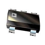
ICGOO电子元器件商城为您提供AD8628ARTZ-R2由Analog设计生产,在icgoo商城现货销售,并且可以通过原厂、代理商等渠道进行代购。 AD8628ARTZ-R2价格参考。AnalogAD8628ARTZ-R2封装/规格:线性 - 放大器 - 仪表,运算放大器,缓冲器放大器, Zero-Drift Amplifier 1 Circuit Rail-to-Rail SOT-23-5。您可以下载AD8628ARTZ-R2参考资料、Datasheet数据手册功能说明书,资料中有AD8628ARTZ-R2 详细功能的应用电路图电压和使用方法及教程。
AD8628ARTZ-R2是Analog Devices Inc.推出的一款零漂移、低噪声、低功耗精密运算放大器,属于线性放大器中的高性能运算放大器类别。其典型应用场景包括精密信号调理、传感器接口、医疗设备、工业控制和便携式仪器等。

该器件具有极低的输入失调电压和温漂,适合需要高精度放大的场合。例如,在电子秤、压力传感器、热电偶信号调理电路中,AD8628ARTZ-R2可有效放大微弱信号并保持信号完整性。在医疗设备如心电图(ECG)监测仪中,其低噪声和低失真特性有助于提升信号采集的准确性。

此外,该运放采用单电源供电,输入输出支持轨至轨操作,适用于电池供电的便携式设备,如数据采集系统、手持测试仪器等。其小型化封装(如SOT-23)也使其适合空间受限的应用环境。

综上,AD8628ARTZ-R2广泛应用于对精度、稳定性和功耗有严苛要求的工业、医疗及消费类电子产品中。
| 参数 | 数值 |
| -3db带宽 | 2.5MHz |
| 产品目录 | 集成电路 (IC)半导体 |
| 描述 | IC OPAMP ZRO-DRFT 2.5MHZ SOT23-5精密放大器 Zero-Drift RRIO SGL-Supply |
| 产品分类 | Linear - Amplifiers - Instrumentation, OP Amps, Buffer Amps集成电路 - IC |
| 品牌 | Analog Devices Inc |
| 产品手册 | |
| 产品图片 |
|
| rohs | 符合RoHS无铅 / 符合限制有害物质指令(RoHS)规范要求 |
| 产品系列 | 放大器 IC,精密放大器,Analog Devices AD8628ARTZ-R2- |
| 数据手册 | |
| 产品型号 | AD8628ARTZ-R2 |
| 产品培训模块 | http://www.digikey.cn/PTM/IndividualPTM.page?site=cn&lang=zhs&ptm=30008http://www.digikey.cn/PTM/IndividualPTM.page?site=cn&lang=zhs&ptm=26202 |
| 产品种类 | 精密放大器 |
| 供应商器件封装 | SOT-23-5 |
| 共模抑制比—最小值 | 140 dB |
| 其它名称 | AD8628ARTZ-R2TR |
| 包装 | 带卷 (TR) |
| 压摆率 | 1 V/µs |
| 双重电源电压 | 1.35 V to 2.5 V |
| 可用增益调整 | 145 dB |
| 商标 | Analog Devices |
| 增益带宽生成 | 2.5 MHz |
| 增益带宽积 | 2.5MHz |
| 安装类型 | 表面贴装 |
| 安装风格 | SMD/SMT |
| 封装 | Reel |
| 封装/外壳 | SC-74A,SOT-753 |
| 封装/箱体 | SOT-23-5 |
| 工作温度 | -40°C ~ 125°C |
| 工作电源电压 | 2.7 V to 5 V |
| 工厂包装数量 | 250 |
| 放大器类型 | 零漂移 |
| 最大双重电源电压 | 2.5 V |
| 最大工作温度 | + 125 C |
| 最小双重电源电压 | 1.35 V |
| 最小工作温度 | - 40 C |
| 标准包装 | 250 |
| 电压-电源,单/双 (±) | 2.7 V ~ 5 V, ±1.35 V ~ 2.5 V |
| 电压-输入失调 | 1µV |
| 电压增益dB | 145 dB |
| 电流-电源 | 850µA |
| 电流-输入偏置 | 30pA |
| 电流-输出/通道 | 30mA |
| 电源电压-最大 | 5 V |
| 电源电压-最小 | 2.7 V |
| 电源电流 | 1 mA |
| 电源类型 | Single, Dual |
| 电路数 | 1 |
| 系列 | AD8628 |
| 视频文件 | http://www.digikey.cn/classic/video.aspx?PlayerID=1364138032001&width=640&height=505&videoID=2245193153001http://www.digikey.cn/classic/video.aspx?PlayerID=1364138032001&width=640&height=505&videoID=2245193159001 |
| 设计资源 | 点击此处下载产品Datasheet点击此处下载产品Datasheet点击此处下载产品Datasheet点击此处下载产品Datasheet点击此处下载产品Datasheet |
| 转换速度 | 1 V/us |
| 输入偏压电流—最大 | 100 pA |
| 输入电压范围—最大 | 5 V |
| 输入补偿电压 | 1 uV |
| 输出电流 | 30 mA |
| 输出类型 | 满摆幅 |
| 通道数量 | 1 Channel |


- 商务部:美国ITC正式对集成电路等产品启动337调查
- 曝三星4nm工艺存在良率问题 高通将骁龙8 Gen1或转产台积电
- 太阳诱电将投资9.5亿元在常州建新厂生产MLCC 预计2023年完工
- 英特尔发布欧洲新工厂建设计划 深化IDM 2.0 战略
- 台积电先进制程称霸业界 有大客户加持明年业绩稳了
- 达到5530亿美元!SIA预计今年全球半导体销售额将创下新高
- 英特尔拟将自动驾驶子公司Mobileye上市 估值或超500亿美元
- 三星加码芯片和SET,合并消费电子和移动部门,撤换高东真等 CEO
- 三星电子宣布重大人事变动 还合并消费电子和移动部门
- 海关总署:前11个月进口集成电路产品价值2.52万亿元 增长14.8%


PDF Datasheet 数据手册内容提取
Zero-Drift, Single-Supply, Rail-to-Rail Input/Output Operational Amplifier Data Sheet AD8628/AD8629/AD8630 FEATURES PIN CONFIGURATIONS Lowest auto-zero amplifier noise Low offset voltage: 1 µV OUT 1 AD8628 5 V+ Input offset drift: 0.002 µV/°C V– 2 TOP VIEW (Not to Scale) R5 aVi ls-tinog-rlaei-ls iunpppulty a onpde orauttipount swing +IN 3 4 –IN 02735-001 High gain, CMRR, and PSRR: 130 dB Figure 1. 5-Lead TSOT (UJ-5) and 5-Lead SOT-23 (RJ-5) Very low input bias current: 100 pA maximum Low supply current: 1.0 mA Overload recovery time: 50 µs NC 1 8 NC No external components required –IN 2 AD8628 7 V+ Qualified for automotive applications +IN 3 TOP VIEW 6 OUT V– N4C (=N oNtO to C SOcNaNleE)CT5 NC 02735-002 APPLICATIONS Figure 2. 8-Lead SOIC_N (R-8) Automotive sensors Pressure and position sensors Strain gage amplifiers OUT A 1 8 V+ Medical instrumentation –IN A 2 AD8629 7 OUT B TPPhrheeocrtimosidooicnoo dcueup ralreme naptml isfpeielnirfssiie nrgs +INV A– 34 (NToOt Pto V SIEcWale) 65 –+IINN BB 02735-063 Figure 3. 8-Lead SOIC_N (R-8) and 8-Lead MSOP (RM-8) GENERAL DESCRIPTION This amplifier has ultralow offset, drift, and bias current. OUT A 1 14 OUT D –IN A 2 13 –IN D The AD8628/AD8629/AD8630 are wide bandwidth auto-zero +IN A 3 AD8630 12 +IN D amplifiers featuring rail-to-rail input and output swing and low V+ 4 TOP VIEW 11 V– noise. Operation is fully specified from 2.7 V to 5 V single supply +IN B 5 (Not to Scale) 10 +IN C (T±h1e. 3A5D V8 6to2 8±/2A.5D V86 d2u9a/Al sDup86p3ly0) .p rovide benefits previously O–UINT BB 67 98 –OIUNT C C 02735-066 found only in expensive auto-zeroing or chopper-stabilized Figure 4. 14-Lead SOIC_N (R-14) and 14-Lead TSSOP (RU-14) amplifiers. Using Analog Devices, Inc., topology, these zero- drift amplifiers combine low cost with high accuracy and low The AD8628/AD8629/AD8630 are specified for the extended noise. No external capacitor is required. In addition, the AD8628/ industrial temperature range (−40°C to +125°C). The AD8628 AD8629/AD8630 greatly reduce the digital switching noise is available in tiny 5-lead TSOT, 5-lead SOT-23, and 8-lead found in most chopper-stabilized amplifiers. narrow SOIC plastic packages. The AD8629 is available in the With an offset voltage of only 1 µV, drift of less than 0.005 μV/°C, standard 8-lead narrow SOIC and MSOP plastic packages. The and noise of only 0.5 µV p-p (0 Hz to 10 Hz), the AD8628/ AD8630 quad amplifier is available in 14-lead narrow SOIC and AD8629/AD8630 are suited for applications where error 14-lead TSSOP plastic packages. See the Ordering Guide for sources cannot be tolerated. Position and pressure sensors, automotive grades. medical equipment, and strain gage amplifiers benefit greatly from nearly zero drift over their operating temperature range. Many systems can take advantage of the rail-to-rail input and output swings provided by the AD8628/AD8629/AD8630 to reduce input biasing complexity and maximize SNR. Rev. K Document Feedback Information furnished by Analog Devices is believed to be accurate and reliable. However, no responsibility is assumed by Analog Devices for its use, nor for any infringements of patents or other One Technology Way, P.O. Box 9106, Norwood, MA 02062-9106, U.S.A. rights of third parties that may result from its use. Specifications subject to change without notice. No license is granted by implication or otherwise under any patent or patent rights of Analog Devices. Tel: 781.329.4700 ©2002–2014 Analog Devices, Inc. All rights reserved. Trademarks and registered trademarks are the property of their respective owners. Technical Support www.analog.com
AD8628/AD8629/AD8630 Data Sheet TABLE OF CONTENTS Features .............................................................................................. 1 Peak-to-Peak Noise .................................................................... 16 Applications ....................................................................................... 1 Noise Behavior with First-Order, Low-Pass Filter ................. 16 General Description ......................................................................... 1 Total Integrated Input-Referred Noise for First-Order Filter16 Pin Configurations ........................................................................... 1 Input Overvoltage Protection ................................................... 17 Revision History ............................................................................... 3 Output Phase Reversal ............................................................... 17 Specifications ..................................................................................... 4 Overload Recovery Time .......................................................... 17 Electrical Characteristics—V = 5.0 V ....................................... 4 Infrared Sensors .......................................................................... 18 S Electrical Characteristics—V = 2.7 V ....................................... 5 Precision Current Shunt Sensor ............................................... 19 S Absolute Maximum Ratings ............................................................ 6 Output Amplifier for High Precision DACs ........................... 19 Thermal Characteristics .............................................................. 6 Outline Dimensions ....................................................................... 20 ESD Caution .................................................................................. 6 Ordering Guide .......................................................................... 22 Typical Performance Characteristics ............................................. 7 Automotive Products ................................................................. 22 Functional Description .................................................................. 15 1/f Noise ....................................................................................... 15 Rev. K | Page 2 of 24
Data Sheet AD8628/AD8629/AD8630 REVISION HISTORY 8/14—Rev. J to Rev. K 1/05—Rev. C to Rev. D Changes to Figure 36 and Figure 37 ............................................. 12 Added AD8630 ................................................................... Universal Added Figure 5 and Figure 6 ........................................................... 1 2/14—Rev. I to Rev. J Changes to Caption in Figure 8 and Figure 9 ................................ 7 Moved Revision History ................................................................... 3 Changes to Caption in Figure 14 .................................................... 8 Changes to Figure 17 and Figure 18 ............................................... 9 Changes to Figure 17 ........................................................................ 8 Updated Outline Dimensions ........................................................ 20 Changes to Figure 23 and Figure 24 ............................................... 9 4/11—Rev. H to Rev. I Changes to Figure 25 and Figure 26 ............................................. 10 Changes to Figure 31 ...................................................................... 11 Updated Outline Dimensions ........................................................ 19 Changes to Figure 40, Figure 41, Figure 42 ................................. 12 Changes to Ordering Guide ........................................................... 21 Changes to Figure 43 and Figure 44 ............................................. 13 4/10—Rev. G to Rev. H Changes to Figure 51 ...................................................................... 15 Change to Features List .................................................................... 1 Updated Outline Dimensions........................................................ 20 Change to General Description Section ......................................... 1 Changes to Ordering Guide ........................................................... 20 Changes to Table 3 ............................................................................ 5 10/04—Rev. B to Rev. C Updated Outline Dimensions Section .......................................... 19 Updated Formatting .......................................................... Universal Changes to Ordering Guide ........................................................... 21 Added AD8629 ................................................................... Universal 6/08—Rev. F to Rev. G Added SOIC and MSOP Pin Configurations ................................ 1 Changes to Features Section ............................................................ 1 Added Figure 48 .............................................................................. 13 Changes to Table 5 and Figure 42 Caption .................................. 12 Changes to Figure 62 ...................................................................... 17 Changes to 1/f Noise Section and Figure 49 ................................ 14 Added MSOP Package .................................................................... 19 Changes to Figure 51 Caption and Figure 55 .............................. 15 Changes to Ordering Guide ........................................................... 22 Changes to Figure 57 Caption and Figure 58 Caption ............... 16 10/03—Rev. A to Rev. B Changes to Figure 60 Caption and Figure 61 Caption ............... 17 Changes to General Description ..................................................... 1 Changes to Figure 64 ...................................................................... 18 Changes to Absolute Maximum Ratings........................................ 4 2/08—Rev. E to Rev. F Changes to Ordering Guide ............................................................. 4 Renamed TSOT-23 to TSOT ............................................ Universal Added TSOT-23 Package ............................................................... 15 Deleted Figure 4 and Figure 6 .......................................................... 1 6/03—Rev. 0 to Rev. A Changes to Figure 3 and Figure 4 Captions ................................... 1 Changes to Specifications................................................................. 3 Changes to Table 1 ............................................................................ 3 Changes to Ordering Guide ............................................................. 4 Changes to Table 2 ............................................................................ 4 Change to Functional Description................................................ 10 Changes to Table 4 ............................................................................ 5 Updated Outline Dimensions........................................................ 15 Updated Outline Dimensions ........................................................ 19 Changes to Ordering Guide ........................................................... 20 10/02—Revision 0: Initial Version 5/05—Rev. D to Rev. E Changes to Ordering Guide ........................................................... 22 Rev. K | Page 3 of 24
AD8628/AD8629/AD8630 Data Sheet SPECIFICATIONS ELECTRICAL CHARACTERISTICS—V = 5.0 V S V = 5.0 V, V = 2.5 V, T = 25°C, unless otherwise noted. S CM A Table 1. Parameter Symbol Conditions Min Typ Max Unit INPUT CHARACTERISTICS Offset Voltage V 1 5 µV OS −40°C ≤ T ≤ +125°C 10 µV A Input Bias Current I B AD8628/AD8629 30 100 pA AD8630 100 300 pA −40°C ≤ T ≤ +125°C 1.5 nA A Input Offset Current I 50 200 pA OS −40°C ≤ T ≤ +125°C 250 pA A Input Voltage Range 0 5 V Common-Mode Rejection Ratio CMRR V = 0 V to 5 V 120 140 dB CM −40°C ≤ T ≤ +125°C 115 130 dB A Large Signal Voltage Gain A R = 10 kΩ, V = 0.3 V to 4.7 V 125 145 dB VO L O −40°C ≤ T ≤ +125°C 120 135 dB A Offset Voltage Drift ∆V /∆T −40°C ≤ T ≤ +125°C 0.002 0.02 µV/°C OS A OUTPUT CHARACTERISTICS Output Voltage High V R = 100 kΩ to ground 4.99 4.996 V OH L −40°C ≤ T ≤ +125°C 4.99 4.995 V A R = 10 kΩ to ground 4.95 4.98 V L −40°C ≤ T ≤ +125°C 4.95 4.97 V A Output Voltage Low V R = 100 kΩ to V+ 1 5 mV OL L −40°C ≤ T ≤ +125°C 2 5 mV A R = 10 kΩ to V+ 10 20 mV L −40°C ≤ T ≤ +125°C 15 20 mV A Short-Circuit Limit I ±25 ±50 mA SC −40°C ≤ T ≤ +125°C ±40 mA A Output Current I ±30 mA O −40°C ≤ T ≤ +125°C ±15 mA A POWER SUPPLY Power Supply Rejection Ratio PSRR V = 2.7 V to 5.5 V, −40°C ≤ T ≤ +125°C 115 130 dB S A Supply Current per Amplifier I V = V/2 0.85 1.1 mA SY O S −40°C ≤ T ≤ +125°C 1.0 1.2 mA A INPUT CAPACITANCE C IN Differential 1.5 pF Common Mode 8.0 pF DYNAMIC PERFORMANCE Slew Rate SR R = 10 kΩ 1.0 V/µs L Overload Recovery Time 0.05 ms Gain Bandwidth Product GBP 2.5 MHz NOISE PERFORMANCE Voltage Noise e p-p 0.1 Hz to 10 Hz 0.5 µV p-p n 0.1 Hz to 1.0 Hz 0.16 µV p-p Voltage Noise Density e f = 1 kHz 22 nV/√Hz n Current Noise Density i f = 10 Hz 5 fA/√Hz n Rev. K | Page 4 of 24
Data Sheet AD8628/AD8629/AD8630 ELECTRICAL CHARACTERISTICS—V = 2.7 V S V = 2.7 V, V = 1.35 V, V = 1.4 V, T = 25°C, unless otherwise noted. S CM O A Table 2. Parameter Symbol Conditions Min Typ Max Unit INPUT CHARACTERISTICS Offset Voltage V 1 5 µV OS −40°C ≤ T ≤ +125°C 10 µV A Input Bias Current I B AD8628/AD8629 30 100 pA AD8630 100 300 pA −40°C ≤ T ≤ +125°C 1.0 1.5 nA A Input Offset Current I 50 200 pA OS −40°C ≤ T ≤ +125°C 250 pA A Input Voltage Range 0 2.7 V Common-Mode Rejection Ratio CMRR V = 0 V to 2.7 V 115 130 dB CM −40°C ≤ T ≤ +125°C 110 120 dB A Large Signal Voltage Gain A R = 10 kΩ, V = 0.3 V to 2.4 V 110 140 dB VO L O −40°C ≤ T ≤ +125°C 105 130 dB A Offset Voltage Drift ∆V /∆T −40°C ≤ T ≤ +125°C 0.002 0.02 µV/°C OS A OUTPUT CHARACTERISTICS Output Voltage High V R = 100 kΩ to ground 2.68 2.695 V OH L −40°C ≤ T ≤ +125°C 2.68 2.695 V A R = 10 kΩ to ground 2.67 2.68 V L −40°C ≤ T ≤ +125°C 2.67 2.675 V A Output Voltage Low V R = 100 kΩ to V+ 1 5 mV OL L −40°C ≤ T ≤ +125°C 2 5 mV A R = 10 kΩ to V+ 10 20 mV L −40°C ≤ T ≤ +125°C 15 20 mV A Short-Circuit Limit I ±10 ±15 mA SC −40°C ≤ T ≤ +125°C ±10 mA A Output Current I ±10 mA O −40°C ≤ T ≤ +125°C ±5 mA A POWER SUPPLY Power Supply Rejection Ratio PSRR V = 2.7 V to 5.5 V, −40°C ≤ T ≤ +125°C 115 130 dB S A Supply Current per Amplifier I V = V/2 0.75 1.0 mA SY O S −40°C ≤ T ≤ +125°C 0.9 1.2 mA A INPUT CAPACITANCE C IN Differential 1.5 pF Common Mode 8.0 pF DYNAMIC PERFORMANCE Slew Rate SR R = 10 kΩ 1 V/µs L Overload Recovery Time 0.05 ms Gain Bandwidth Product GBP 2 MHz NOISE PERFORMANCE Voltage Noise e p-p 0.1 Hz to 10 Hz 0.5 µV p-p n Voltage Noise Density e f = 1 kHz 22 nV/√Hz n Current Noise Density i f = 10 Hz 5 fA/√Hz n Rev. K | Page 5 of 24
AD8628/AD8629/AD8630 Data Sheet ABSOLUTE MAXIMUM RATINGS Table 3. Parameter Rating THERMAL CHARACTERISTICS Supply Voltage 6 V θ is specified for worst-case conditions, that is, θ is specified JA JA Input Voltage GND – 0.3 V to V + 0.3 V S for the device soldered in a circuit board for surface-mount Differential Input Voltage1 ±5.0 V packages. This was measured using a standard two-layer board. Output Short-Circuit Duration to GND Indefinite Storage Temperature Range −65°C to +150°C Table 4. Operating Temperature Range −40°C to +125°C Package Type θJA θJC Unit Junction Temperature Range −65°C to +150°C 5-Lead TSOT (UJ-5) 207 61 °C/W Lead Temperature (Soldering, 60 sec) 300°C 5-Lead SOT-23 (RJ-5) 230 146 °C/W ESD AD8628 8-Lead SOIC_N (R-8) 158 43 °C/W HBM 8-Lead SOIC ±7000V 8-Lead MSOP (RM-8) 190 44 °C/W FICDM 8-Lead SOIC ±1500V 14-Lead SOIC_N (R-14) 105 43 °C/W FICDM 5-Lead TSOT ±1000V 14-Lead TSSOP (RU-14) 148 23 °C/W MM 8-Lead SOIC ±200V ESD AD8629 ESD CAUTION HBM 8-Lead SOIC ±4000V FICDM 8-Lead SOIC ±1000V ESD AD8630 HBM 14-Lead SOIC ±5000V FICDM 14-Lead SOIC ±1500V FICDM 14-Lead TSSOP ±1500V MM 14-Lead SOIC ±200V 1 Differential input voltage is limited to ±5 V or the supply voltage, whichever is less. Stresses above those listed under Absolute Maximum Ratings may cause permanent damage to the device. This is a stress rating only; functional operation of the device at these or any other conditions above those indicated in the operational section of this specification is not implied. Exposure to absolute maximum rating conditions for extended periods may affect device reliability. Rev. K | Page 6 of 24
Data Sheet AD8628/AD8629/AD8630 TYPICAL PERFORMANCE CHARACTERISTICS 180 100 VS = 2.7V VS = 5V 160 TA = 25°C 90 VCM = 2.5V TA = 25°C 80 140 S S R R E E 70 FI 120 FI PLI PLI 60 M 100 M A A F F 50 ER O 80 ER O 40 B B M 60 M U U 30 N N 40 20 20 10 0–2.5 –1.5 INPUT –O0F.5FSET VOL0T.A5GE (µV) 1.5 2.5 02735-003 0–2.5 –1.5 INPUT –O0F.5FSET VOL0T.A5GE (µV) 1.5 2.5 02735-006 Figure 5. Input Offset Voltage Distribution Figure 8. Input Offset Voltage Distribution 60 7 VS = 5V +85°C VS = 5V 50 6 TA = –40°CTO +125°C A) S ENT (p 40 LIFIER 5 RR MP 4 U A S C 30 OF BIA ER 3 UT 20 MB P +25°C U 2 N N I 10 –40°C 1 00 1 INPUT C2OMMON-M3ODE VOLT4AGE (V) 5 6 02735-004 00 2 T4CVOS (nV/°C6) 8 10 02735-007 Figure 6. AD8628 Input Bias Current vs. Input Common-Mode Voltage Figure 9. Input Offset Voltage Drift 1500 1k VS = 5V 150°C TVAS == 255V°C 1000 100 pA) 125°C V) CURRENT ( 5000 OLTAGE (m 10 SOURCE UT BIAS –500 UTPUT V 1 SINK P O N I 0.1 –1000 –15000 1 INPUT C2OMMON-M3ODE VOLT4AGE (V) 5 6 02735-005 0.001.0001 0.001 LO0A.0D1 CURRENT0 .(1mA) 1 10 02735-008 Figure 7. AD8628 Input Bias Current vs. Input Common-Mode Voltage Figure 10. Output Voltage to Supply Rail vs. Load Current Rev. K | Page 7 of 24
AD8628/AD8629/AD8630 Data Sheet 1k 1000 VS = 2.7V TA = 25°C 100 800 mV) µA) E ( T ( G 10 N 600 A E T SOURCE R L R VO SINK CU UT 1 LY 400 P P T P U U O S 0.1 200 0.001.0001 0.001 LO0A.0D1 CURRENT0 .(1mA) 1 10 02735-009 00 1 2SUPPLY VO3LTAGE (V4) 5 6 02735-012 Figure 11. Output Voltage to Supply Rail vs. Load Current Figure 14. Supply Current vs. Supply Voltage 1500 VS = 5V VS = 2.7V VCM = 2.5V 60 CL = 20pF 1150 TA = –40°CTO +150°C RL = ∞ NPUT BIAS CURRENT (pA) 940500 OPEN-LOOP GAIN (dB) 42000 PHASGEAIN ФM = 45° 49110503850 PHASE SHIFT (Degrees) I 100 225 –20 0–50 –25 0 25TEMP5E0RATU7R5E (°C1)00 125 150 175 02735-010 10k 100kFREQUENCY (Hz)1M 10M 02735-013 Figure 12. AD8628 Input Bias Current vs. Temperature Figure 15. Open-Loop Gain and Phase vs. Frequency 1250 70 TA = 25°C VS = 5V 5V 60 CL = 20pF 1000 RL = ∞ 50 ΦM = 52.1° CURRENT (µA)SUPPLY 755000 2.7V OPEN-LOOP GAIN (dB) 432100000 PHASGEAIN 49110503850 PHASE SHIFT (Degrees) 250 –10 225 –20 0–50 0 TE5M0PERATURE1 0(0°C) 150 200 02735-011 –3010k 100k FREQUENCY (1HMz) 10M 02735-014 Figure 13. Supply Current vs. Temperature Figure 16. Open-Loop Gain and Phase vs. Frequency Rev. K | Page 8 of 24
Data Sheet AD8628/AD8629/AD8630 70 300 VS = 2.7V VS = 5V 60 CL = 20pF 270 RL = 2kΩ 50 240 B) AV = 100 Ω) GAIN (d 4300 ANCE ( 211800 OP 20 AV = 10 PED 150 O M CLOSED-L 100 AV = 1 OUTPUT I 12900 –10 60 AV = 100 AV = 10 –20 30 AV = 1 –301k 10k FRE1Q0U0EkNCY (Hz) 1M 10M 02735-015 0100 1k 10kFREQU1E00NkCY (Hz)1M 10M 100M 02735-018 Figure 17. Closed-Loop Gain vs. Frequency Figure 20. Output Impedance vs. Frequency 70 VS = 5V 60 CL = 20pF RL = 2kΩ 50 B) AV = 100 N (d 40 DIV) AI 30 V/ VS = ±1.35V LOOP G 20 AV = 10 E (500m 0V CRALLV === 3∞100pF SED- 10 AV = 1 LTAG LO 0 VO C –10 –20 –301k 10k FREQU1E00NkCY (Hz) 1M 10M 02735-016 TIME (4µs/DIV) 02735-019 Figure 18. Closed-Loop Gain vs. Frequency Figure 21. Large Signal Transient Response 300 VS = 2.7V 270 240 Ω) CE ( 210 V) N 180 DI VS = ±2.5V MPEDA 150 GE (1V/ 0V CRALLV === 3∞100pF UT I 120 LTA P O UT 90 V O 60 AV = 10 AV = 100 30 AV = 1 0100 1k 10kFREQU1E00NkCY (Hz)1M 10M 100M 02735-017 TIME (5µs/DIV) 02735-020 Figure 19. Output Impedance vs. Frequency Figure 22. Large Signal Transient Response Rev. K | Page 9 of 24
AD8628/AD8629/AD8630 Data Sheet 80 VS = ±2.5V VCSL == ±510.p3F5V 70 RTAL == 225k°ΩC RL = ∞ AV = 1 60 mV/DIV) OT (%) 50 GE (50 0V RSHO 40 LTA OVE 30 O OS– V 20 OS+ 10 TIME (4µs/DIV) 02735-021 01 C10APACITIVE LOAD (p1F0)0 1k 02735-024 Figure 23. Small Signal Transient Response Figure 26. Small Signal Overshoot vs. Load Capacitance CVRASLLV ==== ±5∞120.p5FV VIN VARCCSHLVL 1==== =±10– 20p55.k0F05ΩmVV/DIV V) CH2 = 1V/DIV mV/DI E (V) 0V 0 G E (5 0V LTA G O TA V 0V L O V VOUT TIME (4µs/DIV) 02735-022 TIME (2µs/DIV) 02735-025 Figure 24. Small Signal Transient Response Figure 27. Positive Overvoltage Recovery 100 VS = ±1.35V 90 RL = 2kΩ 0V TA = 25°C 80 VS = ±2.5V AV = –50 70 RL = 10kΩ RSHOOT (%) 6500 OS– OLTAGE (V)VOVUINT CCCHHL 12= ==0 p51F0Vm/DVIV/DIV VE 40 V O OS+ 30 20 0V 10 01 C10APACITIVE LOAD (p1F0)0 1k 02735-023 TIME (10µs/DIV) 02735-026 Figure 25. Small Signal Overshoot vs. Load Capacitance Figure 28. Negative Overvoltage Recovery Rev. K | Page 10 of 24
Data Sheet AD8628/AD8629/AD8630 140 VS = ±2.5V 120 VS = ±1.35V VIN = 1kHz @ ±3V p-p CL = 0pF 100 RL = 10kΩ AV = 1 80 V) LTAGE (1V/DI 0V PSRR (dB) 642000 –PSRR+PSRR O V 0 –20 –40 TIME (200µs/DIV) 02735-027 –60100 1k F1R0EkQUENCY1 (0H0zk) 1M 10M 02735-030 Figure 29. No Phase Reversal Figure 32. PSRR vs. Frequency 140 140 VS = 2.7V VS = ±2.5V 120 120 100 100 80 80 CMRR (dB) 642000 PSRR (dB) 642000 –PSRR +PSRR 0 0 –20 –20 –40 –40 –60100 1k F1R0EkQUENCY1 (0H0zk) 1M 10M 02735-028 –60100 1k F1R0EkQUENCY1 (0H0zk) 1M 10M 02735-031 Figure 30. CMRR vs. Frequency Figure 33. PSRR vs. Frequency 140 3.0 VS = 5V VS = 2.7V 120 RL = 10kΩ 2.5 TA = 25°C 100 AV = 1 p) 80 V p- 2.0 B) 60 G ( d N MRR ( 40 T SWI 1.5 C 20 PU UT 1.0 0 O –20 0.5 –40 –60100 1k F1R0EkQUENCY1 (0H0zk) 1M 10M 02735-029 0100 1k FREQUE10NkCY (Hz) 100k 1M 02735-032 Figure 31. CMRR vs. Frequency Figure 34. Maximum Output Swing vs. Frequency Rev. K | Page 11 of 24
AD8628/AD8629/AD8630 Data Sheet 5.5 120 45..50 VRTAASLV ==== 25115V0°kCΩ √Hz) 105 VNSO I=S 2E.7AVT 1kHz = 21.3nV p) 4.0 nV/ 90 G (V p- 3.5 NSITY ( 75 N 3.0 E UT SWI 2.5 OISE D 60 OUTP 21..05 AGE N 45 T 30 L 1.0 VO 15 0.5 0100 1k FREQUE10NkCY (Hz) 100k 1M 02735-033 00 0.5 FR1E.0QUENCY (1k.H5z) 2.0 2.5 02735-036 Figure 35. Maximum Output Swing vs. Frequency Figure 38. Voltage Noise Density at 2.7 V from 0 Hz to 2.5 kHz 0.60 120 VS = 2.7V VS = 2.7V 0.45 105 NOISEAT 10kHz = 42.4nV Hz) √ 0.30 V/ 90 n Y ( E (µV) 0.15 ENSIT 75 AG 0 E D 60 OLT OIS V–0.15 N 45 E G A –0.30 LT 30 O V –0.45 15 –0.60 TIME (1s/DIV) 02735-034 00 5 FR1E0QUENCY (k1H5z) 20 25 02735-037 Figure 36. 0.1 Hz to 10 Hz Noise Figure 39. Voltage Noise Density at 2.7 V from 0 Hz to 25 kHz 0.60 120 VS = 5V VS = 5V 0.45 105 NOISEAT 1kHz = 22.1nV Hz) √ 0.30 V/ 90 n Y ( AGE (µV) 0.150 E DENSIT 7650 T S OL OI V–0.15 E N 45 G A –0.30 LT 30 O V –0.45 15 –0.60 TIME (1s/DIV) 02735-035 00 0.5 FR1E.0QUENCY (1k.H5z) 2.0 2.5 02735-038 Figure 37. 0.1 Hz to 10 Hz Noise Figure 40. Voltage Noise Density at 5 V from 0 Hz to 2.5 kHz Rev. K | Page 12 of 24
Data Sheet AD8628/AD8629/AD8630 120 150 V/√Hz) 10950 NVSO I=S 5EVAT 10kHz = 36.4nV ENT (mA) 100 TVAS == –24.70V°CTO +150°C n R ENSITY ( 75 UIT CUR 50 SE D 60 CIRC ISC– NOI 45 RT- 0 TAGE 30 T SHO ISC+ L U O P –50 V T 15 OU 00 5 FR1E0QUENCY (k1H5z) 20 25 02735-039 –100–50 –25 0 25TEMP5E0RATU7R5E (°C1)00 125 150 175 02735-042 Figure 41. Voltage Noise Density at 5 V from 0 Hz to 25 kHz Figure 44. Output Short-Circuit Current vs. Temperature 120 150 V/√Hz) 10950 VS = 5V ENT (mA) 100 VTAS == –54V0°CTO +150°C n R ENSITY ( 75 UIT CUR 50 ISC– SE D 60 CIRC NOI 45 RT- 0 TAGE 30 T SHO L U O P –50 V T 15 OU ISC+ 00 FREQUE5NCY (kHz) 10 02735-040 –100–50 –25 0 25TEMP5E0RATU7R5E (°C1)00 125 150 175 02735-043 Figure 42. Voltage Noise Density at 5 V from 0 Hz to 10 kHz Figure 45. Output Short-Circuit Current vs. Temperature 150 1k VS = 5V 140 TION (dB) 113200 VTAS == –24.70V°CTOTO 5 V+125°C AGE (mV) 100 VOL– VEE@VC 1Ck–Ω VOH@ 1kΩ C T E 110 L EJ VO VCC– VOH@ 10kΩ PLY R 100 RAIL 10 VOL– VEE@ 10kΩ ER SUP 9800 PUT-TO- VCC– VOH@ 100kΩ POW 70 OUT 1 VOL– VEE@ 100kΩ 60 50–50 –25 0 TEM2P5ERATUR5E0 (°C) 75 100 125 02735-041 0.1–50 –25 0 25TEMP5E0RATU7R5E (°C1)00 125 150 175 02735-044 Figure 43. Power Supply Rejection vs. Temperature Figure 46. Output-to-Rail Voltage vs. Temperature Rev. K | Page 13 of 24
AD8628/AD8629/AD8630 Data Sheet 1k 140 VS = 2.7V VS = ±2.5V 120 AGE (mV) 100 VCC– VOH@ V1kOΩL– VEE@ 1kΩ ON (dB) 100 LT TI AIL VO 10 VCC– VOH@ 10kΩ EPARA 80 R1 OUTPUT-TO-R 1 VCC– VOH@ 10V0kOΩL– VEEVO@L 1–0 V0EkEΩ@ 10kΩ CHANNEL S 6400 28mV pV-IpN –+ +2A.5VVV–+ VOUT VV1+–0kBΩ 10R02Ω 20 –2.5V 0.1–50 –25 0 25TEMP5E0RATU7R5E (°C1)00 125 150 175 02735-045 01k 10k FREQU1E0N0kCY (Hz) 1M 10M 02735-062 Figure 47. Output-to-Rail Voltage vs. Temperature Figure 48. AD8629/AD8630 Channel Separation vs. Frequency Rev. K | Page 14 of 24
Data Sheet AD8628/AD8629/AD8630 FUNCTIONAL DESCRIPTION The AD8628/AD8629/AD8630 are single-supply, ultrahigh 1/f NOISE precision rail-to-rail input and output operational amplifiers. 1/f noise, also known as pink noise, is a major contributor to The typical offset voltage of less than 1 µV allows these amplifiers errors in dc-coupled measurements. This 1/f noise error term to be easily configured for high gains without risk of excessive can be in the range of several µV or more, and, when amplified output voltage errors. The extremely small temperature drift with the closed-loop gain of the circuit, can show up as a large of 2 nV/°C ensures a minimum offset voltage error over their output offset. For example, when an amplifier with a 5 µV p-p entire temperature range of −40°C to +125°C, making these 1/f noise is configured for a gain of 1000, its output has 5 mV of amplifiers ideal for a variety of sensitive measurement applica- error due to the 1/f noise. However, the AD8628/AD8629/AD8630 tions in harsh operating environments. eliminate 1/f noise internally, thereby greatly reducing output errors. The AD8628/AD8629/AD8630 achieve a high degree of precision The internal elimination of 1/f noise is accomplished as follows. through a patented combination of auto-zeroing and chopping. 1/f noise appears as a slowly varying offset to the AD8628/AD8629/ This unique topology allows the AD8628/AD8629/AD8630 to AD8630 inputs. Auto-zeroing corrects any dc or low frequency maintain their low offset voltage over a wide temperature range offset. Therefore, the 1/f noise component is essentially removed, and over their operating lifetime. The AD8628/AD8629/AD8630 leaving the AD8628/AD8629/AD8630 free of 1/f noise. also optimize the noise and bandwidth over previous generations One advantage that the AD8628/AD8629/AD8630 bring to of auto-zero amplifiers, offering the lowest voltage noise of any system applications over competitive auto-zero amplifiers is their auto-zero amplifier by more than 50%. very low noise. The comparison shown in Figure 49 indicates Previous designs used either auto-zeroing or chopping to add an input-referred noise density of 19.4 nV/√Hz at 1 kHz for precision to the specifications of an amplifier. Auto-zeroing the AD8628, which is much better than the Competitor A results in low noise energy at the auto-zeroing frequency, at the and Competitor B. The noise is flat from dc to 1.5 kHz, slowly expense of higher low frequency noise due to aliasing of wideband increasing up to 20 kHz. The lower noise at low frequency is noise into the auto-zeroed frequency band. Chopping results in desirable where auto-zero amplifiers are widely used. lower low frequency noise at the expense of larger noise energy 120 at the chopping frequency. The AD8628/AD8629/AD8630 family uses both auto-zeroing and chopping in a patented ping- 105 COMPETITOR A Hz) (89.7nV/√Hz) pong arrangement to obtain lower low frequency noise together √ V/ 90 with lower energy at the chopping and auto-zeroing frequencies, Y (n maximizing the signal-to-noise ratio for the majority of SIT 75 N applications without the need for additional filtering. The DE E 60 relatively high clock frequency of 15 kHz simplifies filter S OI requirements for a wide, useful noise-free bandwidth. N 45 COMPETITOR B GE (31.1nV/√Hz) The AD8628 is among the few auto-zero amplifiers offered in TA 30 L the 5-lead TSOT package. This provides a significant improvement VO over the ac parameters of the previous auto-zero amplifiers. The 15 AD8628 MK AT 1kHz FOR ALL 3 GRAPHS (19.4nV/√Hz) AbaDn8d6w2i8d/tAh D(08 6H2z9 t/oA 1D08 k6H30z )h aavned lcoawn nboei sues eodv ewr hae rreel athtiev ehlyig wheidste 00 2 F4REQUENC6Y (kHz) 8 10 12 02735-046 dc precision is required. In systems with signal bandwidths of Figure 49. Noise Spectral Density of AD8628 vs. Competition from 5 kHz to 10 kHz, the AD8628/AD8629/AD8630 provide true 16-bit accuracy, making them the best choice for very high resolution systems. Rev. K | Page 15 of 24
AD8628/AD8629/AD8630 Data Sheet PEAK-TO-PEAK NOISE 50 45 Because of the ping-pong action between auto-zeroing and chopping, the peak-to-peak noise of the AD8628/AD8629/ 40 AD8630 is much lower than the competition. Figure 50 and 35 Figure 51 show this comparison. B) 30 d E ( 25 S en p-p = 0.5µV OI BW = 0.1HzTO 10Hz N 20 15 V) 10 DI µV/ 5 5 0. LTAGE ( 00 10 20 30 FR4E0QUE5N0CY (6k0Hz) 70 80 90 100 02735-050 VO Figure 53. Simulation Transfer Function of the Test Circuit in Figure 52 50 45 TIME (1s/DIV) 02735-047 4305 Figure 50. AD8628 Peak-to-Peak Noise B) 30 d SE ( 25 OI N 20 en p-p = 2.3µV 15 BW = 0.1HzTO 10Hz 10 V) 5 DI E (0.5µV/ 00 10 20 30 FR4E0QUE5N0CY (6k0Hz) 70 80 90 100 02735-051 G Figure 54. Actual Transfer Function of the Test Circuit in Figure 52 A T L VO The measured noise spectrum of the test circuit charted in Figure 54 shows that noise between 5 kHz and 45 kHz is successfully rolled off by the first-order filter. TOTAL INTEGRATED INPUT-REFERRED NOISE FOR TIME (1s/DIV) 02735-048 FIRST-ORDER FILTER Figure 51. Competitor A Peak-to-Peak Noise For a first-order filter, the total integrated noise from the AD8628 is lower than the noise of Competitor A. NOISE BEHAVIOR WITH FIRST-ORDER, LOW-PASS FILTER 10 The AD8628 was simulated as a low-pass filter (see Figure 53) and then configured as shown in Figure 52. The behavior of the COMPETITOR A AD8628 matches the simulated data. It was verified that noise is V) rolled off by first-order filtering. Figure 53 and Figure 54 show E (µ AD8551 AD8628 the difference between the simulated and actual transfer functions OIS 1 N of the circuit shown in Figure 52. S M R IN OUT 100kΩ 470pF 1kΩ 02735-049 0.110 3dB10 F0ILTER BANDWIDTH1 k(Hz) 10k 02735-052 Figure 52. First-Order Low-Pass Filter Test Circuit, Figure 55. RMS Noise vs. 3 dB Filter Bandwidth in Hz ×101 Gain and 3 kHz Corner Frequency Rev. K | Page 16 of 24
Data Sheet AD8628/AD8629/AD8630 INPUT OVERVOLTAGE PROTECTION CH1 = 50mV/DIV Although the AD8628/AD8629/AD8630 are rail-to-rail input VIN CAHV 2= =– 510V/DIV amplifiers, care should be taken to ensure that the potential difference between the inputs does not exceed the supply voltage. Under normal negative feedback operating conditions, the V) 0V amplifier corrects its output to ensure that the two inputs are at GE ( A the same voltage. However, if either input exceeds either supply LT O rail by more than 0.3 V, large currents begin to flow through the V 0V ESD protection diodes in the amplifier. These diodes are connected between the inputs and each supply rail to protect the input transistors against an electrostatic discharge VOUT evvoeltnatg, ea nexdc teheedys athree nsuoprmplayl vlyo rlteavgeer,s teh-ebsiaes EedSD. H doiwodeevse rc,a inf tbheec ionmpuet TIME (500µs/DIV) 02735-053 forward-biased. Without current limiting, excessive amounts Figure 56. Positive Input Overload Recovery for the AD8628 of current could flow through these diodes, causing permanent damage to the device. If inputs are subject to overvoltage, appropriate series resistors should be inserted to limit the diode CH1 = 50mV/DIV current to less than 5 mA maximum. CH2 = 1V/DIV VIN AV = –50 OUTPUT PHASE REVERSAL Output phase reversal occurs in some amplifiers when the input V) 0V common-mode voltage range is exceeded. As common-mode E ( G voltage is moved outside the common-mode range, the outputs of A T L these amplifiers can suddenly jump in the opposite direction to O V 0V the supply rail. This is the result of the differential input pair shutting down, causing a radical shifting of internal voltages that results in the erratic output behavior. The AD8628/AD8629/AD8630 amplifiers have been carefully VOUT dboesthig ninepdu ttos aprree vmenaitn atnayin oeudt pwuitth pihna tshee r seuvpeprslayl v, polrtoavgiedse. dIf t ohnate or TIME (500µs/DIV) 02735-054 Figure 57. Positive Input Overload Recovery for Competitor A both inputs could exceed either supply voltage, a resistor should be placed in series with the input to limit the current to less than 5 mA. This ensures that the output does not reverse its phase. CH1 = 50mV/DIV OVERLOAD RECOVERY TIME CH2 = 1V/DIV VIN AV = –50 Many auto-zero amplifiers are plagued by a long overload recovery time, often in ms, due to the complicated settling behavior of the internal nulling loops after saturation of the outputs. The V) 0V E ( AD8628/AD8629/AD8630 have been designed so that internal G A T settling occurs within two clock cycles after output saturation L O V 0V occurs. This results in a much shorter recovery time, less than 10 µs, when compared to other auto-zero amplifiers. The wide bandwidth of the AD8628/AD8629/AD8630 enhances performance when the parts are used to drive loads that inject VOUT tarmanpsliiefnietrs iisn tuos ethde t oou dtpriuvtes . tThhe iisn ips ua tc oofm smwiotnch seitdu actaiponac withore nA aDnC s. TIME (500µs/DIV) 02735-055 Figure 58. Positive Input Overload Recovery for Competitor B Rev. K | Page 17 of 24
AD8628/AD8629/AD8630 Data Sheet The results shown in Figure 56 to Figure 61 are summarized in Table 5. 0V CH1 = 50mV/DIV CH2 = 1V/DIV Table 5. Overload Recovery Time AV = –50 Positive Overload Negative Overload V) VIN Model Recovery (µs) Recovery (µs) E ( G AD8628 6 9 A T OL Competitor A 650 25,000 VVOUT Competitor B 40,000 35,000 INFRARED SENSORS 0V Infrared (IR) sensors, particularly thermopiles, are increasingly TIME (500µs/DIV) 02735-056 braeninggin ugs aesd aiunt otemmopteivreat culrime mateea csounretrmole, nhtu fmora anp epalirc tahtieornmso ams wetiedres , Figure 59. Negative Input Overload Recovery for the AD8628 home insulation analysis, and automotive repair diagnostics. The relatively small output signal of the sensor demands high gain with very low offset voltage and drift to avoid dc errors. 0V CH1 = 50mV/DIV If interstage ac coupling is used, as in Figure 62, low offset and CH2 = 1V/DIV drift prevent the output of the input amplifier from drifting close to AV = –50 VIN saturation. The low input bias currents generate minimal errors VOUT from the output impedance of the sensor. As with pressure sensors, V) E ( the very low amplifier drift with time and temperature eliminate G A additional errors once the temperature measurement is calibrated. T L O The low 1/f noise improves SNR for dc measurements taken V 0V over periods often exceeding one-fifth of a second. Figure 62 shows a circuit that can amplify ac signals from 100 µV to 300 µV up to the 1 V to 3 V levels, with a gain of 10,000 for accurate analog-to-digital conversion. TIME (500µs/DIV) 02735-057 100Ω 100kΩ 10kΩ 100kΩ Figure 60. Negative Input Overload Recovery for Competitor A 5V 5V 100µV TO 300µV 10µF IR 1/2 AD8629 DETECTOR 1/2 AD8629 10kΩ 0V fC ≈1.6Hz CCAHHV 12= ==– 55100Vm/DVIV/DIV VTOOL TBAIAGSE 02735-059 V) VIN Figure 62. AD8629 Used as Preamplifier for Thermopile E ( AGVOUT T L O V 0V TIME (500µs/DIV) 02735-058 Figure 61. Negative Input Overload Recovery for Competitor B Rev. K | Page 18 of 24
Data Sheet AD8628/AD8629/AD8630 PRECISION CURRENT SHUNT SENSOR OUTPUT AMPLIFIER FOR HIGH PRECISION DACS A precision current shunt sensor benefits from the unique The AD8628/AD8629/AD8630 are used as output amplifiers for attributes of auto-zero amplifiers when used in a differencing a 16-bit high precision DAC in a unipolar configuration. In this configuration, as shown in Figure 63. Current shunt sensors are case, the selected op amp needs to have a very low offset voltage used in precision current sources for feedback control systems. (the DAC LSB is 38 μV when operated with a 2.5 V reference) They are also used in a variety of other applications, including to eliminate the need for output offset trims. The input bias battery fuel gauging, laser diode power measurement and control, current (typically a few tens of picoamperes) must also be very torque feedback controls in electric power steering, and precision low because it generates an additional zero code error when power metering. multiplied by the DAC output impedance (approximately 6 kΩ). Rail-to-rail input and output provide full-scale output with very SUPPLY I 0R.1SΩ RL lciottdlee einrdroerp.e Tnhdee notu, btpuut tt hime hpiegdha inncpeu ot fi mthpee dDaAnCce ios fc tohnes AtaDnt8 6an28d/ 100kΩ 100Ω AD8629/AD8630 minimizes gain errors. The wide bandwidth e = 1000 RSI of the amplifiers also serves well in this case. The amplifiers, 100mV/mA C 5V with settling time of 1 μs, add another time constant to the system, increasing the settling time of the output. The settling time of the AD5541 is 1 μs. The combined settling time is AD8628 approximately 1.4 μs, as can be derived from the following 100kΩ 100Ω equation: C 02735-060 tSTOTAL tS DAC2tSAD86282 Figure 63. Low-Side Current Sensing In such applications, it is desirable to use a shunt with very low 5V 2.5V 10µF resistance to minimize the series voltage drop; this minimizes wasted power and allows the measurement of high currents 0.1µF 0.1µF while saving power. A typical shunt might be 0.1 Ω. At measured current values of 1 A, the output signal of the shunt is hundreds of millivolts, or even volts, and amplifier error sources are not INTSEERRFIAALCE VDD REF(REFF*) REFS* critical. However, at low measured current values in the 1 mA CS AD8628 DIN UNIPOLAR range, the 100 μV output voltage of the shunt demands a very SCLK AD5541/AD5542 VOUT OUTPUT low offset voltage and drift to maintain absolute accuracy. Low LDAC* idnopeus tn boita bs eccuormreen at ss iagrnei failcsaon tn peeerdceedn,t asoge t hofa tt hine jmecetaesdu rbeidas c cuurrrernent.t *AD5542 ONLY DGND AGND 02735-061 Figure 64. AD8628 Used as an Output Amplifier High open-loop gain, CMRR, and PSRR help to maintain the overall circuit accuracy. As long as the rate of change of the current is not too fast, an auto-zero amplifier can be used with excellent results. Rev. K | Page 19 of 24
AD8628/AD8629/AD8630 Data Sheet OUTLINE DIMENSIONS 2.90 BSC 5.00(0.1968) 4.80(0.1890) 5 4 8 5 1.60 BSC 2.80 BSC 4.00(0.1574) 6.20(0.2441) 1 2 3 3.80(0.1497) 1 4 5.80(0.2284) 0.95 BSC 1.27(0.0500) 0.50(0.0196) 1.90 BSC 1.75(0.0688) 0.25(0.0099) 45° *00..7900 MMIANX BSC 0.25(0.0098) 1.35(0.0532) 8° 0.10(0.0040) 0° *1.00 MAX 00..2008 COPL0A.1N0ARITSYEATING 00..5311((00..00210212)) 0.25(0.0098) 10..2470((00..00510507)) 8° PLANE 0.17(0.0067) 0.10 MAX 0.50 SEATING 4° 0.60 0.30 PLANE 0° 0.45 COMPLIANTTOJEDECSTANDARDSMS-012-AA *CTHOEM PEXLICAENPTT TIOON J OEDF EPCA CSTKAANGDEA HREDIGS HMTO A-1N9D3 -TAHBICWKINTHESS. 0.30 100708-A C(RINEOFNPEATRRREOENNLCLTEIHNEOGSNDELISYM)AEANNRDSEIAORRNOESUNANORDETEDAIN-POMPFRIFLOLMPIMIRLELIATIMTEEERTFSEO;RIRNECUQHSUEDIVIINMAELDENENSSTIIOGSNNFS.OR 012407-A Figure 65. 5-Lead Thin Small Outline Transistor Package [TSOT] Figure 67. 8-Lead Standard Small Outline Package [SOIC_N] (UJ-5) Narrow Body Dimensions shown in millimeters (R-8) Dimensions shown in millimeters and (inches) 3.00 3.20 2.90 3.00 2.80 2.80 1.70 5 4 3.00 1.60 2.80 8 5 5.15 1.50 2.60 3.20 4.90 1 2 3 3.00 4.65 2.80 1 4 0.95BSC PIN 1 B1.S9C0 IDENTIFIER 1.30 0.65 BSC 1.15 0.90 1.45MAX 0.20MAX 0.95 15° MAX 0.95MIN 0.08MIN 0.85 1.10 MAX 0.55 0.75 00..1055MMAINX Figure 66C. 5O-MLPeLaIA00dN..53 ST05mTMMOAIaNXJlEl DOEuCtSPSliELTnAAAeTNNI ENTDGAraRnDSsiMstOo-1r7 P8a-A1c50A0°°k°age [B0S.S6OC0T-23] 00..4355 11-01-2010-A CO00P..10L550A.1N0ARICTOYMPLIANT00.. 42T05O JEDEC STA60°°NDARDS 00M..20O39-187-AA 000...854050 10-07-2009-B (RJ-5) Figure 68. 8-Lead Mini Small Outline Package [MSOP] Dimensions shown in millimeters (RM-8) Dimensions shown in millimeters Rev. K | Page 20 of 24
Data Sheet AD8628/AD8629/AD8630 5.10 5.00 8.75 (0.3445) 4.90 8.55 (0.3366) 14 8 43..0800 ((00..11547956)) 114 78 65..2800 ((00..22424813)) 44..5400 6.40 BSC 4.30 1 0.25 (0.0098) 1.27 B(0S.C0500) 11..7355 ((00..00658391)) 8° 00..5205 ((00..00109978)) 45° PIN 1 7 0.10 (0.0039) 0° 0.65 BSC COPL0A.1N0ARITY 00..5311 ((00..00210212)) SPELAATNIENG 00..2157 ((00..00009687)) 10..2470 ((00..00510507)) 11..0050 1M.2A0X 0.20 0.80 0.09 0.75 C(RINOEFNPEATRRREOENNLCLTEIHNC EOGOSN MEDLSIPYM)LAEAIANNRNDSETI AORTRNOOESU JNANEORDDEETE DAICN-P O SMPFTRIFALO NLMPIDIMRLAELIRATIMDTEESER TFMSEO;S RIR-N 0 ECU1Q2HS-U EADI VBIINMA LEDENENSSTIIOGSN NFS.OR 060606-A COPL0A00...1N10055ARITY 00C..O3109MPLIANT TO JEDSPEELCAA TNSIETNAGNDARDS MO-801°°53-AB-1 00..6405 061908-A Figure 69. 14-Lead Standard Small Outline Package [SOIC_N] Figure 70. 14-Lead Thin Shrink Small Outline Package [TSSOP] Narrow Body (R-14) (RU-14) Dimensions shown in millimeters and (inches) Dimensions shown in millimeters Rev. K | Page 21 of 24
AD8628/AD8629/AD8630 Data Sheet ORDERING GUIDE Model1, 2 Temperature Range Package Description Package Option Branding AD8628AUJ-REEL −40°C to +125°C 5-Lead TSOT UJ-5 AYB AD8628AUJ-REEL7 −40°C to +125°C 5-Lead TSOT UJ-5 AYB AD8628AUJZ-R2 −40°C to +125°C 5-Lead TSOT UJ-5 A0L AD8628AUJZ-REEL −40°C to +125°C 5-Lead TSOT UJ-5 A0L AD8628AUJZ-REEL7 −40°C to +125°C 5-Lead TSOT UJ-5 A0L AD8628ARZ −40°C to +125°C 8-Lead SOIC_N R-8 AD8628ARZ-REEL −40°C to +125°C 8-Lead SOIC_N R-8 AD8628ARZ-REEL7 −40°C to +125°C 8-Lead SOIC_N R-8 AD8628ARTZ-R2 −40°C to +125°C 5-Lead SOT-23 RJ-5 A0L AD8628ARTZ-REEL7 −40°C to +125°C 5-Lead SOT-23 RJ-5 A0L AD8628WARZ-RL −40°C to +125°C 8-Lead SOIC_N R-8 A0L AD8628WARZ-R7 −40°C to +125°C 8-Lead SOIC_N R-8 A0L AD8628WARTZ-RL −40°C to +125°C 5-Lead SOT-23 RJ-5 A0L AD8628WARTZ-R7 −40°C to +125°C 5-Lead SOT-23 RJ-5 A0L AD8628WAUJZ-RL −40°C to +125°C 5-Lead TSOT UJ-5 A0L AD8628WAUJZ-R7 −40°C to +125°C 5-Lead TSOT UJ-5 A0L AD8629ARZ −40°C to +125°C 8-Lead SOIC_N R-8 AD8629ARZ-REEL −40°C to +125°C 8-Lead SOIC_N R-8 AD8629ARZ-REEL7 −40°C to +125°C 8-Lead SOIC_N R-8 AD8629ARMZ −40°C to +125°C 8-Lead MSOP RM-8 A06 AD8629ARMZ-REEL −40°C to +125°C 8-Lead MSOP RM-8 A06 AD8629WARZ-RL −40°C to +125°C 8-Lead SOIC_N R-8 AD8629WARZ-R7 −40°C to +125°C 8-Lead SOIC_N R-8 AD8630ARUZ −40°C to +125°C 14-Lead TSSOP RU-14 AD8630ARUZ-REEL −40°C to +125°C 14-Lead TSSOP RU-14 AD8630ARZ −40°C to +125°C 14-Lead SOIC_N R-14 AD8630ARZ-REEL −40°C to +125°C 14-Lead SOIC_N R-14 AD8630ARZ-REEL7 −40°C to +125°C 14-Lead SOIC_N R-14 AD8630WARZ-RL −40°C to +125°C 14-Lead SOIC_N R-14 AD8630WARZ-R7 −40°C to +125°C 14-Lead SOIC_N R-14 1 Z = RoHS Compliant Part. 2 W = Qualified for Automotive Applications. AUTOMOTIVE PRODUCTS The AD8628W/AD8629W/AD8630W models are available with controlled manufacturing to support the quality and reliability requirements of automotive applications. Note that these automotive models may have specifications that differ from the commercial models; therefore, designers should review the Specifications section of this data sheet carefully. Only the automotive grade products shown are available for use in automotive applications. Contact your local Analog Devices account representative for specific product ordering information and to obtain the specific Automotive Reliability reports for these models. Rev. K | Page 22 of 24
Data Sheet AD8628/AD8629/AD8630 NOTES Rev. K | Page 23 of 24
AD8628/AD8629/AD8630 Data Sheet NOTES ©2002–2014 Analog Devices, Inc. All rights reserved. Trademarks and registered trademarks are the property of their respective owners. D02735-0-8/14(K) Rev. K | Page 24 of 24
Mouser Electronics Authorized Distributor Click to View Pricing, Inventory, Delivery & Lifecycle Information: A nalog Devices Inc.: AD8628ARTZ-R2 AD8628ARTZ-REEL7 AD8628ARZ AD8628AUJZ-R2 AD8630ARUZ AD8630ARZ AD8628ARZ- REEL AD8628ARZ-REEL7 AD8628WARTZ-R7 AD8628WARTZ-RL AD8628WARZ-R7 AD8628WARZ-RL AD8630ARUZ-REEL AD8630ARZ-REEL AD8630ARZ-REEL7 AD8630WARZ-R7 AD8630WARZ-RL AD8628AUJZ- REEL AD8628AUJZ-REEL7 AD8628WAUJZ-R7 AD8628WAUJZ-RL AD8628AUJ-REEL7 AD8628AUJ-REEL