ICGOO在线商城 > 集成电路(IC) > 线性 - 放大器 - 仪表,运算放大器,缓冲器放大器 > AD8574AR

 Datasheet下载
- 型号: AD8574AR
- 制造商: Analog
- 库位|库存: xxxx|xxxx
- 要求:
| 数量阶梯 | 香港交货 | 国内含税 |
| +xxxx | $xxxx | ¥xxxx |
查看当月历史价格
查看今年历史价格
AD8574AR产品简介:
ICGOO电子元器件商城为您提供AD8574AR由Analog设计生产,在icgoo商城现货销售,并且可以通过原厂、代理商等渠道进行代购。 AD8574AR价格参考¥29.34-¥30.69。AnalogAD8574AR封装/规格:线性 - 放大器 - 仪表,运算放大器,缓冲器放大器, 零漂移 放大器 4 电路 满摆幅 14-SOIC。您可以下载AD8574AR参考资料、Datasheet数据手册功能说明书,资料中有AD8574AR 详细功能的应用电路图电压和使用方法及教程。
AD8574AR 是 Analog Devices Inc. 生产的一款高精度、低功耗的运算放大器,具有轨到轨输入输出特性,适用于多种工业与仪器仪表应用场景。

该器件广泛应用于传感器信号调理、精密测量设备、数据采集系统以及工业自动化控制中。由于其低失调电压、低温漂和高共模抑制比(CMRR),特别适合用于压力传感器、温度传感器、称重传感器等微弱信号的放大处理。

此外,AD8574AR 也常用于便携式设备和电池供电系统,因其低功耗特性可有效延长设备工作时间。在医疗电子设备、测试与测量仪器、过程控制系统中也有广泛应用。

总结来说,AD8574AR 的主要应用场景包括:
1. 传感器接口与信号调理
2. 工业自动化与过程控制
3. 精密数据采集系统
4. 医疗仪器与分析设备
5. 电池供电及低功耗便携设备
| 参数 | 数值 |
| -3db带宽 | - |
| 产品目录 | 集成电路 (IC)半导体 |
| 描述 | IC OPAMP CHOPPER 1.5MHZ 14SOIC精密放大器 Zero-Drft SGL-Supply RRIO Quad |
| 产品分类 | Linear - Amplifiers - Instrumentation, OP Amps, Buffer Amps集成电路 - IC |
| 品牌 | Analog Devices |
| 产品手册 | |
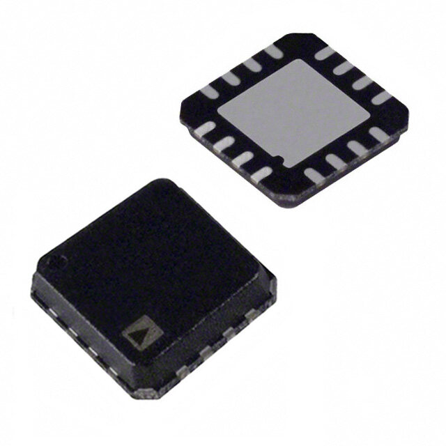
| 产品图片 |
|
| rohs | 否不符合限制有害物质指令(RoHS)规范要求 |
| 产品系列 | 放大器 IC,精密放大器,Analog Devices AD8574AR- |
| 数据手册 | |
| 产品型号 | AD8574AR |
| PCN过时产品 | |
| 产品培训模块 | http://www.digikey.cn/PTM/IndividualPTM.page?site=cn&lang=zhs&ptm=30008http://www.digikey.cn/PTM/IndividualPTM.page?site=cn&lang=zhs&ptm=26202 |
| 产品种类 | 精密放大器 |
| 供应商器件封装 | 14-SOIC |
| 共模抑制比—最小值 | 140 dB |
| 包装 | 管件 |
| 压摆率 | 0.4 V/µs |
| 可用增益调整 | 145 dB |
| 商标 | Analog Devices |
| 增益带宽生成 | 1.5 MHz |
| 增益带宽积 | 1.5MHz |
| 安装类型 | 表面贴装 |
| 安装风格 | SMD/SMT |
| 封装 | Tube |
| 封装/外壳 | 14-SOIC(0.154",3.90mm 宽) |
| 封装/箱体 | SOIC-14 |
| 工作温度 | -40°C ~ 125°C |
| 工作电源电压 | 2.7 V to 6 V |
| 工厂包装数量 | 56 |
| 放大器类型 | 断路器(零漂移) |
| 最大工作温度 | + 125 C |
| 最小工作温度 | - 40 C |
| 标准包装 | 56 |
| 电压-电源,单/双 (±) | 2.7 V ~ 5.5 V |
| 电压-输入失调 | 1µV |
| 电压增益dB | 145 dB |
| 电流-电源 | 850µA |
| 电流-输入偏置 | 10pA |
| 电流-输出/通道 | 30mA |
| 电源电压-最大 | 6 V |
| 电源电压-最小 | 2.7 V |
| 电源电流 | 3.9 mA |
| 电源类型 | Single |
| 电路数 | 4 |
| 系列 | AD8574 |
| 视频文件 | http://www.digikey.cn/classic/video.aspx?PlayerID=1364138032001&width=640&height=505&videoID=2245193153001http://www.digikey.cn/classic/video.aspx?PlayerID=1364138032001&width=640&height=505&videoID=2245193159001 |
| 输入偏压电流—最大 | 1.5 nA |
| 输入补偿电压 | 1 uV |
| 输出类型 | 满摆幅 |
| 通道数量 | 4 Channel |


- 商务部:美国ITC正式对集成电路等产品启动337调查
- 曝三星4nm工艺存在良率问题 高通将骁龙8 Gen1或转产台积电
- 太阳诱电将投资9.5亿元在常州建新厂生产MLCC 预计2023年完工
- 英特尔发布欧洲新工厂建设计划 深化IDM 2.0 战略
- 台积电先进制程称霸业界 有大客户加持明年业绩稳了
- 达到5530亿美元!SIA预计今年全球半导体销售额将创下新高
- 英特尔拟将自动驾驶子公司Mobileye上市 估值或超500亿美元
- 三星加码芯片和SET,合并消费电子和移动部门,撤换高东真等 CEO
- 三星电子宣布重大人事变动 还合并消费电子和移动部门
- 海关总署:前11个月进口集成电路产品价值2.52万亿元 增长14.8%


PDF Datasheet 数据手册内容提取
Zero-Drift, Single-Supply, Rail-to-Rail Input/Output Operational Amplifiers Data Sheet AD8571/AD8572/AD8574 FEATURES PIN CONFIGURATIONS Low offset voltage: 1 μV NC 1 8 NC Input offset drift: 0.005 μV/°C –IN A 2 AD8571 7 V+ Rail-to-rail input and output swing +IN A 3 TOP VIEW 6 OUT A (Not to Scale) 5H iVg/h2 .g7a Vin s:i n14g5le d-sBu tpyppliyc aolp eration V– 4NC = NO CONNECT5 NC 01104-001 CMRR: 140 dB typical Figure 1. 8-Lead MSOP (RM Suffix) PSRR: 130 dB typical Ultralow input bias current: 10 pA typical NC 1 8 NC Low supply current: 750 μA per op amp –IN A 2 AD8571 7 V+ +IN A 3 TOP VIEW 6 OUT A ON ove erxloteardn rael ccoavpearcyi ttoimrse r:e 5q0u μirse d V– N4C (=N oNtO to C SOcNaNleE)CT5 NC 01104-004 Figure 2. 8-Lead SOIC (R Suffix) APPLICATIONS Temperature sensors OUT A 1 8 V+ –IN A 2 AD8572 7 OUT B PPStrrreeascisinsui gorean gs ceeun arsrmoenrpstl isfieenrssi ng +INV A– 34 (NToOt Pto V SIEcWale) 65 –+IINN BB 01104-002 Figure 3. 8-Lead TSSOP (RU Suffix) Medical instrumentation Thermocouple amplifiers OUT A 1 8 V+ –IN A 2 AD8572 7 OUT B GENERAL DESCRIPTION +INV A– 34 (NToOt Pto V SIEcWale) 65 –+IINN BB 01104-005 Figure 4. 8-Lead SOIC (R Suffix) This family of amplifiers has ultralow offset, drift, and bias current. The AD8571/AD8572/AD85741 are single, dual, and OUT A 1 14 OUT D quad amplifiers, respectively, featuring rail-to-rail input and –IN A 2 13 –IN D output swings. All are guaranteed to operate from 2.7 V to 5 V +IN A 3 AD8574 12 +IN D single supply. V+ 4 TOP VIEW 11 V– +IN B 5 (Not to Scale) 10 +IN C Tfohuen Ad Don8l5y7 i1n/ AexDp8e5n7s2iv/eA aDu8to5-7z4e prorionvgid oer bcehnoepfpitesr p-srteavbiioluizselyd O –UINT BB 67 98 –OIUNT C C 01104-003 amplifiers. Using Analog Devices, Inc., topology, these zero- Figure 5. 14-Lead TSSOP (RU Suffix) drift amplifiers combine low cost with high accuracy. (No OUT A 1 14 OUT D external capacitors are required.) Using a spread-spectrum, –IN A 2 13 –IN D auto-zero technique, the AD8571/AD8572/AD8574 eliminate +IN A 3 AD8574 12 +IN D the intermodulation effects from interaction of the chopping V+ 4 TOP VIEW 11 V– function with the signal frequency in ac applications. +IN B 5 (Not to Scale) 10 +IN C With an offset voltage of only 1 μV and drift of 0.005 μV/°C, the O –UINT BB 67 98 –OIUNT C C 01104-006 AD8571/AD8572/AD8574 are perfectly suited for applications Figure 6. 14-Lead SOIC (R Suffix) where error sources cannot be tolerated. Position and pressure The AD8571/AD8572/AD8574 are specified for the extended sensors, medical equipment, and strain gage amplifiers benefit industrial/ automotive temperature range (−40°C to +125°C). greatly from nearly zero drift over their operating temperature The AD8571 single amplifier is available in 8-lead MSOP and range. Many more systems require the rail-to-rail input and narrow SOIC packages. The AD8572 dual amplifier is available in output swings provided by the AD8571/AD8572/AD8574. 8-lead narrow SOIC and surface-mount TSSOP packages. The AD8574 quad amplifier is available in 14-lead narrow SOIC and TSSOP packages. 1 Protected by U.S. Patent 6,130,578. Rev. F Document Feedback Information furnished by Analog Devices is believed to be accurate and reliable. However, no responsibility is assumed by Analog Devices for its use, nor for any infringements of patents or other One Technology Way, P.O. Box 9106, Norwood, MA 02062-9106, U.S.A. rights of third parties that may result from its use. Specifications subject to change without notice. No license is granted by implication or otherwise under any patent or patent rights of Analog Devices. Tel: 781.329.4700 ©1999–2015 Analog Devices, Inc. All rights reserved. Trademarks and registered trademarks are the property of their respective owners. Technical Support www.analog.com
AD8571/AD8572/AD8574 Data Sheet TABLE OF CONTENTS Features .............................................................................................. 1 Maximizing Performance Through Proper Layout ............... 17 Applications ....................................................................................... 1 1/f Noise Characteristics ........................................................... 18 General Description ......................................................................... 1 Random Auto-Zero Correction Eliminates Intermodulation Distortion .................................................................................... 18 Pin Configurations ........................................................................... 1 Broadband and External Resistor Noise Considerations .......... 19 Revision History ............................................................................... 3 Output Overdrive Recovery ...................................................... 19 Specifications ..................................................................................... 4 Input Overvoltage Protection ................................................... 19 5 V Electrical Characteristics ...................................................... 4 Output Phase Reversal ............................................................... 19 2.7 V Electrical Characteristics ................................................... 5 Capacitive Load Drive ............................................................... 20 Absolute Maximum Ratings ............................................................ 6 Power-Up Behavior .................................................................... 20 Thermal Characteristics .............................................................. 6 Applications Information .............................................................. 21 ESD Caution .................................................................................. 6 5 V Precision Strain Gage Circuit ............................................ 21 Typical Performance Characteristics ............................................. 7 3 V Instrumentation Amplifier ................................................ 21 Functional Description .................................................................. 15 High Accuracy Thermocouple Amplifier ............................... 22 Amplifier Architecture .............................................................. 15 Precision Current Meter ............................................................ 22 Basic Auto-Zero Amplifier Theory .......................................... 15 Precision Voltage Comparator .................................................. 22 Auto-Zero Phase ......................................................................... 16 Outline Dimensions ....................................................................... 23 Amplification Phase ................................................................... 16 Ordering Guide .......................................................................... 25 High Gain, CMRR, and PSRR .................................................. 17 Rev. F | Page 2 of 28
Data Sheet AD8571/AD8572/AD8574 REVISION HISTORY 6/15—Rev. E to Rev. F 9/06—Rev. A to Rev. B Added Patent Note, Note 1............................................................... 1 Updated Format ................................................................. Universal Change to Input Voltage Parameter, Table 3.................................. 6 Changes to Table 1 ............................................................................ 3 Changes to Ordering Guide ........................................................... 25 Changes to Table 2 ............................................................................ 4 Changes to Figure 50 ...................................................................... 14 2/11—Rev. D to Rev. E Changes to Figure 51 ...................................................................... 15 Changes to Figure 66 ...................................................................... 21 Changes to Figure 66 ...................................................................... 21 Updated Outline Dimensions ........................................................ 22 Deleted Figure 69 and SPICE Macro-Model Section ................. 17 Changes to Ordering Guide ........................................................... 23 Deleted SPICE Macro-Model for the AD857x Section .............. 18 6/08—Rev. C to Rev. D Updated Outline Dimensions........................................................ 22 Changes to Figure 19 and Figure 20 ............................................... 8 Changes to Ordering Guide ........................................................... 23 Changes to Figure 44 ...................................................................... 12 7/03—Rev. 0 to Rev. A Changes to Figure 38 ...................................................................... 13 Renumbered Figures .......................................................... Universal Moved Figure 50 and Figure 51 ..................................................... 14 Changes to Ordering Guide ............................................................. 4 Changes to Figure 66, Precision Current Meter Section, Layout, Change to Figure 15. ....................................................................... 16 Figure 67, Equation 24, and Figure 68 .......................................... 21 Updated Outline Dimensions........................................................ 19 5/07—Rev. B to Rev. C 10/99—Revision 0: Initial Version Changes to Features .......................................................................... 1 Changes to Table 1 ............................................................................ 3 Changes to Table 2 ............................................................................ 4 Changes to Basic Auto-Zero Amplifier Theory Section ............ 14 Changes to Figure 50 ...................................................................... 15 Changes to Figure 55 ...................................................................... 16 Changes to Figure 66 ...................................................................... 21 Updated Outline Dimensions ........................................................ 22 Rev. F | Page 3 of 28
AD8571/AD8572/AD8574 Data Sheet SPECIFICATIONS 5 V ELECTRICAL CHARACTERISTICS V = 5 V, V = 2.5 V, V = 2.5 V, T = 25°C, unless otherwise noted. S CM O A Table 1. Parameter Symbol Conditions Min Typ Max Unit INPUT CHARACTERISTICS Offset Voltage V 1 5 μV OS −40°C ≤ T ≤ +125°C 10 μV A Input Bias Current I 10 50 pA B AD8571/AD8574 −40°C ≤ T ≤ +125°C 1.0 1.5 nA A AD8572 −40°C ≤ T ≤ +85°C 160 300 pA A −40°C ≤ T ≤ +125°C 2.5 4 nA A Input Offset Current I 20 70 pA OS AD8571/AD8574 −40°C ≤ T ≤ +125°C 150 200 pA A AD8572 −40°C ≤ T ≤ +85°C 30 150 pA A −40°C ≤ T ≤ +125°C 150 400 pA A Input Voltage Range 0 5 V Common-Mode Rejection Ratio CMRR V = 0 V to 5 V 120 140 dB CM −40°C ≤ T ≤ +125°C 115 130 dB A Large Signal Voltage Gain1 A R = 10 kΩ, V = 0.3 V to 4.7 V 125 145 dB VO L O −40°C ≤ T ≤ +125°C 120 135 dB A Offset Voltage Drift ∆V /∆T −40°C ≤ T ≤ +125°C 0.005 0.04 μV/°C OS A OUTPUT CHARACTERISTICS Output Voltage High V R = 100 kΩ to GND 4.99 4.998 V OH L R = 100 kΩ to GND @ −40°C to +125°C 4.99 4.997 V L R = 10 kΩ to GND 4.95 4.98 V L R = 10 kΩ to GND @ −40°C to +125°C 4.95 4.975 V L Output Voltage Low V R = 100 kΩ to V+ 1 10 mV OL L RL = 100 kΩ to V+ @ −40°C to +125°C 2 10 mV R = 10 kΩ to V+ 10 30 mV L R = 10 kΩ to V+ @ −40°C to +125°C 15 30 mV L Short-Circuit Limit I ±25 ±50 mA SC −40°C to +125°C ±40 mA Output Current I ±30 mA O −40°C to +125°C ±15 mA POWER SUPPLY Power Supply Rejection Ratio PSRR V = 2.7 V to 5.5 V 120 130 dB S −40°C ≤ T ≤ +125°C 115 130 dB A Supply Current per Amplifier I V = 0 V 850 975 μA SY O −40°C ≤ T ≤ +125°C 1000 1075 μA A DYNAMIC PERFORMANCE Slew Rate SR R = 10 kΩ 0.4 V/μs L Overload Recovery Time 0.05 0.3 ms Gain Bandwidth Product GBP 1.5 MHz NOISE PERFORMANCE Voltage Noise e p-p 0 Hz to 10 Hz 1.3 μV p-p n 0 Hz to 1 Hz 0.41 μV p-p Voltage Noise Density e f = 1 kHz 51 nV/√Hz n Current Noise Density i f = 10 Hz 2 fA/√Hz n 1 Gain testing is dependent upon test bandwidth. Rev. F | Page 4 of 28
Data Sheet AD8571/AD8572/AD8574 2.7 V ELECTRICAL CHARACTERISTICS V = 2.7 V, V = 1.35 V, V = 1.35 V, T = 25°C, unless otherwise noted. S CM O A Table 2. Parameter Symbol Conditions Min Typ Max Unit INPUT CHARACTERISTICS Offset Voltage V 1 5 μV OS −40°C ≤ T ≤ +125°C 10 μV A Input Bias Current I 10 50 pA B AD8571/AD8574 −40°C ≤ T ≤ +125°C 1.0 1.5 nA A AD8572 −40°C ≤ T ≤ +85°C 160 300 pA A −40°C ≤ T ≤ +125°C 2.5 4 nA A Input Offset Current I 10 50 pA OS AD8571/AD8574 −40°C ≤ T ≤ +125°C 150 200 pA A AD8572 −40°C ≤ T ≤ +85°C 30 150 pA A −40°C ≤ T ≤ +125°C 150 400 pA A Input Voltage Range 0 2.7 V Common-Mode Rejection Ratio CMRR V = 0 V to 2.7 V 115 130 dB CM −40°C ≤ T ≤ +125°C 110 130 dB A Large Signal Voltage Gain1 A R = 10 kΩ, V = 0.3 V to 2.4 V 110 140 dB VO L O −40°C ≤ T ≤ +125°C 105 130 dB A Offset Voltage Drift ∆V /∆T −40°C ≤ T ≤ +125°C 0.005 0.04 µV/°C OS A OUTPUT CHARACTERISTICS Output Voltage High V R = 100 kΩ to GND 2.685 2.697 V OH L R = 100 kΩ to GND @ −40°C to +125°C 2.685 2.696 V L R = 10 kΩ to GND 2.67 2.68 V L R = 10 kΩ to GND @ −40°C to +125°C 2.67 2.675 V L Output Voltage Low V R = 100 kΩ to V+ 1 10 mV OL L R = 100 kΩ to V+ @ −40°C to +125°C 2 10 mV L R = 10 kΩ to V+ 10 20 mV L R = 10 kΩ to V+ @ −40°C to +125°C 15 20 mV L Short-Circuit Limit I ±10 ±15 mA SC −40°C to +125°C ±10 mA Output Current I ±10 mA O −40°C to +125°C ±5 mA POWER SUPPLY Power Supply Rejection Ratio PSRR V = 2.7 V to 5.5 V 120 130 dB S −40°C ≤ T ≤ +125°C 115 130 dB A Supply Current per Amplifier I V = 0 V 750 900 μA SY O −40°C ≤ T ≤ +125°C 950 1000 μA A DYNAMIC PERFORMANCE Slew Rate SR R = 10 kΩ 0.5 V/μs L Overload Recovery Time 0.05 ms Gain Bandwidth Product GBP 1 MHz NOISE PERFORMANCE Voltage Noise e p-p 0 Hz to 10 Hz 2.0 μV p-p n Voltage Noise Density e f = 1 kHz 94 nV/√Hz n Current Noise Density i f = 10 Hz 2 fA/√Hz n 1 Gain testing is dependent upon test bandwidth. Rev. F | Page 5 of 28
AD8571/AD8572/AD8574 Data Sheet ABSOLUTE MAXIMUM RATINGS Stresses at or above those listed under Absolute Maximum Table 3. Ratings may cause permanent damage to the product. This is a Parameter Rating stress rating only; functional operation of the product at these Supply Voltage 6 V or any other conditions above those indicated in the operational Input Voltage GND − 0.3 V to V + 0.3 V S section of this specification is not implied. Operation beyond Differential Input Voltage1 ±5.0 V the maximum operating conditions for extended periods may ESD (Human Body Model) 2000 V affect product reliability. Output Short-Circuit Duration to GND Indefinite Storage Temperature Range −65°C to +150°C THERMAL CHARACTERISTICS Operating Temperature Range −40°C to +125°C θ is specified for the worst-case conditions, that is, θ is Junction Temperature Range −65°C to +150°C JA JA specified for a device soldered in a circuit board for SOIC and Lead Temperature (Soldering, 60 sec) 300°C TSSOP packages. 1 Differential input voltage is limited to ±5.0 V or the supply voltage, whichever is less. Table 4. Thermal Resistance Package Type θ θ Unit JA JC 8-Lead SOIC (R) 158 43 °C/W 8-Lead MSOP (RM) 190 44 °C/W 8-Lead TSSOP (RU) 240 43 °C/W 14-Lead SOIC (R) 120 36 °C/W 14-Lead TSSOP (RU) 180 36 °C/W ESD CAUTION Rev. F | Page 6 of 28
Data Sheet AD8571/AD8572/AD8574 TYPICAL PERFORMANCE CHARACTERISTICS 180 180 VS = 2.7V VS = 5V 160 VCM = 1.35V 160 VCM = 2.5V TA = 25°C TA = 25°C 140 140 S S R R E E FI 120 FI 120 LI LI P P M 100 M 100 A A F F R O 80 R O 80 E E MB 60 MB 60 U U N N 40 40 20 20 –02.5 –1.5 O–F0F.5SET VOL0T.A5GE (µV)1.5 2.5 01104-007 –02.5 –1.5 O–F0F.5SET VOL0T.A5GE (µV)1.5 2.5 01104-010 Figure 7. Input Offset Voltage Distribution Figure 10. Input Offset Voltage Distribution 50 12 VS = 5V 40 TA = –40°C, +25°C, +85°C VS = 5V 10 VCM = 2.5V A) 30 S TA = –40°C TO +125°C RENT (p 20 +85°C PLIFIER 8 R M S CU 10 OF A 6 UT BIA 0 +25°C MBER 4 P U N –10 N I –40°C 2 –20 –300 1INPUT COMM2ON-MODE V3OLTAGE (V4) 5 01104-008 00 1 INPU2T OFFSET3 DRIFT (n4V/°C) 5 6 01104-011 Figure 8. Input Bias Current vs. Input Common-Mode Voltage Figure 11. Input Offset Voltage Drift Distribution 1500 10k VTAS == 152V5°C VTAS == 255V°C 1000 1k NT (pA) 500 E (mV) E G 100 R 0 A R T U L C O T BIAS –500 TPUT V 10 SOURCE SINK U U P–1000 O N I 1 –1500 –20000 1 COMMON2-MODE VOL3TAGE (V) 4 5 01104-009 00.1.0001 0.001 0.L0O1AD CU0R.R1ENT (mA1) 10 100 01104-012 Figure 9. Input Bias Current vs. Common-Mode Voltage Figure 12. Output Voltage to Supply Rail vs. Load Current Rev. F | Page 7 of 28
AD8571/AD8572/AD8574 Data Sheet 10k 800 VTAS == 225.7°VC A) 700 TA = 25°C µ 1k R ( E V) FI 600 m LI GE ( 100 AMP 500 OUTPUT VOLTA 10 SOURCE SINK Y CURRENT PER 234000000 1 PL P SU 100 00.1.0001 0.001 0.L0O1AD CU0R.R1ENT (mA1) 10 100 01104-013 00 1 S2UPPLY VO3LTAGE (4V) 5 6 01104-016 Figure 13. Output Voltage to Supply Rail vs. Load Current Figure 16. Supply Current per Amplifier vs. Supply Voltage 1000 60 VVCS M= =5 V2.5V 50 VCRSLL === 2∞0.p7FV 40 0 A) 750 RENT (p AIN (dB) 2300 4950 Degrees) NPUT BIAS CUR 520500 OPEN-LOOP G –11000 121382505 PHASE SHIFT ( I –20 270 –30 0–75 –50 –25 0TEMP2E5RATU5R0E (°C7)5 100 125 150 01104-014 –4010k 100k FREQU1EMNCY (Hz) 10M 100M 01104-017 Figure 14. Input Bias Current vs. Temperature Figure 17. Open-Loop Gain and Phase Shift vs. Frequency 1.0 60 VS= 5V 5V 50 CRLL == ∞0pF 0.8 40 0 T (mA) 2.7V N (dB) 30 45 grees) SUPPLY CURREN 00..64 OPEN-LOOP GAI –1120000 91120382505 PHASE SHIFT (De 0.2 –20 270 –30 0–75 –50 –25 0TEMP2E5RATU5R0E (°C7)5 100 125 150 01104-015 –4010k 100k FREQU1EMNCY (Hz) 10M 100M 01104-018 Figure 15. Supply Current vs. Temperature Figure 18. Open-Loop Gain and Phase Shift vs. Frequency Rev. F | Page 8 of 28
Data Sheet AD8571/AD8572/AD8574 60 300 50 VCSL == 22.07pVF 270 VS= 5V RL = 2kΩ 40 240 GAIN (dB) 2300 AV = 100 ANCE (Ω) 128100 OOP 10 AV = 10 MPED 150 AV = 100 CLOSED-L –100 AV = 1 OUTPUT I 12900 AV = 10 –20 60 –30 30 AV = 1 –40100 1k F1R0EkQUENCY1 (0H0zk) 1M 10M 01104-019 0100 1k F1R0EkQUENCY1 (0H0zk) 1M 10M 01104-022 Figure 19. Closed-Loop Gain vs. Frequency Figure 22. Output Impedance vs. Frequency 60 50 VCRSLL === 522Vk0ΩpF VCRSLL === 223.k07Ω0VpF 40 AV = 1 B) AV = 100 N (d 30 GAI 20 P AV = 10 O 10 O L D- 0 SE AV = 1 LO –10 C –20 ––4300100 1k F1R0EkQUENCY1 (0H0zk) 1M 10M 01104-020 2µs 500mV 01104-023 Figure 20. Closed-Loop Gain vs. Frequency Figure 23. Large Signal Transient Response 300 270 VS= 2.7V VCSL == 53V00pF RL = 2kΩ 240 AV = 1 Ω) E ( 210 C AN 180 PED 150 AV = 100 M UT I 120 UTP 90 AV = 10 O 60 300100 1k F1R0EkQUENCY1 (0H0zk) A1VM = 1 10M 01104-021 5µs 1V 01104-024 Figure 21. Output Impedance vs. Frequency Figure 24. Large Signal Transient Response Rev. F | Page 9 of 28
AD8571/AD8572/AD8574 Data Sheet 45 CVRSLL === ∞±510.p3F5V %) 40 VRTASL === 2±252k°.Ω5CV AV = 1 T ( 35 O +OS O H 30 S R E V 25 O L A 20 N G –OS L SI 15 L A M 10 S 5µs 50mV 01104-025 0510 10C0APACITANCE (pF)1k 10k 01104-028 Figure 25. Small Signal Transient Response Figure 28. Small Signal Overshoot vs. Load Capacitance CVSL == ±520.p5FV 0V ARLV == ∞1 VIN VVSIN == ±(–R22.E050TVm TVO pG-pND) CL = 0pF RL = 10kΩ AV = –100 VOUT 5µs 50mV 01104-026 0V BTOOPT TSOCMA LSE2C0:A µ2Ls0E0m: 1VV/D/DIVIV 1V 01104-029 Figure 26. Small Signal Transient Response Figure 29. Positive Overvoltage Recovery 50 45 VRTASL === 2±251k°.Ω3C5V VIN %) 40 OT ( 35 0V O VS = ±2.5V OVERSH 3205 +OS VRCILLN === 10(2R0p0kFE0ΩmT VT Op -GpND) L –OS 0V AV = –100 A 20 N G SI 15 L L A 10 M VOUT S 5 20µs 1V 0010 10C0APACITANCE (pF)1k 10k 01104-027 BTOOPT TSOCMA LSEC:A 2L0E0m: 1VV/D/DIVIV 01104-030 Figure 27. Small Signal Overshoot vs. Load Capacitance Figure 30. Negative Overvoltage Recovery Rev. F | Page 10 of 28
Data Sheet AD8571/AD8572/AD8574 140 VS = ±2.5V VS = ±1.35V RALV == 2–k1Ω00 120 VIN = 60mV p-p 100 B) 80 d R ( R PS 60 40 –PSRR +PSRR 20 200µs 1V 01104-031 0100 1k F1R0EkQUENCY1 (0H0zk) 1M 10M 01104-034 Figure 31. No Phase Reversal Figure 34. PSRR vs. Frequency 140 140 VS = 2.7V VS = ±2.5V 120 120 100 100 +PSRR dB) 80 dB) 80 R ( R ( R R CM 60 PS 60 40 40 –PSRR 20 20 0100 1k F1R0EkQUENCY1 (0H0zk) 1M 10M 01104-032 0100 1k F1R0EkQUENCY1 (0H0zk) 1M 10M 01104-035 Figure 32. CMRR vs. Frequency Figure 35. PSRR vs. Frequency 140 3.0 VS = 5V 120 2.5 VS = ±1.35V 100 p) RALV == 21kΩ p- 2.0 THD + N < 1% dB) 80 G (V TA = 25°C RR ( WIN 1.5 CM 60 T S U P T 1.0 40 U O 20 0.5 0 100 1k F1R0EkQUENCY1 (0H0zk) 1M 10M 01104-033 0100 1k FREQU1E0NkCY (Hz) 100k 1M 01104-036 Figure 33. CMRR vs. Frequency Figure 36. Maximum Output Swing vs. Frequency Rev. F | Page 11 of 28
AD8571/AD8572/AD8574 Data Sheet 5.5 VS = ±2.5V 45..50 RATHLV D== +21 kNΩ < 1% 364 RVSS == 20.Ω7V TA = 25°C 312 p) 4.0 p- V 3.5 260 G ( Hz) WIN 3.0 V/ 208 T S 2.5 n (n U e P 2.0 156 T U O 1.5 104 1.0 52 0.5 0100 1k FREQU1E0NkCY (Hz) 100k 1M 01104-037 0 0.5 FR1E.0QUENCY (1k.H5z) 2.0 2.5 01104-040 Figure 37. Maximum Output Swing vs. Frequency Figure 40. Voltage Noise Density from 0 Hz to 2.5 kHz AVSV == ±112.03,50V00 112 VRSS == 20.Ω7V 96 80 Hz) 0V V/ 64 n n ( e 48 32 1sec 50mV 01104-038 160 5 FR1E0QUENCY (k1H5z) 20 25 01104-041 Figure 38. 0.1 Hz to 10 Hz Noise Figure 41. Voltage Noise Density from 0 Hz to 25 kHz VASV == ±122.05,V000 182 RVSS == 50VΩ 156 130 Hz) V/ 104 n n ( e 78 52 1sec 50mV 01104-039 26 0 0.5 FR1E.0QUENCY (1k.H5z) 2.0 2.5 01104-042 Figure 39. 0.1 Hz to 10 Hz Noise Figure 42. Voltage Noise Density from 0 Hz to 2.5 kHz Rev. F | Page 12 of 28
Data Sheet AD8571/AD8572/AD8574 150 112 VS = 5V VS = 2.7V TO 5.5V RS = 0Ω B) d 145 96 N ( O TI en (nV/ Hz) 684408 UPPLY REJEC 114305 S R E 32 W O 130 P 16 0 5 FR1E0QUENCY (k1H5z) 20 25 01104-043 125–75 –50 –25 0TEMP2E5RATU5R0E (°C7)5 100 125 150 01104-045 Figure 43. Voltage Noise Density from 0 Hz to 25 kHz Figure 45. Power Supply Rejection vs. Temperature 50 210 VS = 5V mA) 40 VS = 2.7V RS = 0Ω T ( 30 180 RREN 20 ISC– U V/ Hz) 112500 RCUIT C 100 en (n 90 ORT-CI –10 SH –20 ISC+ 60 PUT –30 T U 30 O –40 0 FREQUE5NCY (Hz) 10 01104-044 –50–75 –50 –25 0TEMP2E5RATU5R0E (°C7)5 100 125 150 01104-046 Figure 44. Voltage Noise Density from 0 Hz to 10 Hz Figure 46. Output Short-Circuit Current vs. Temperature Rev. F | Page 13 of 28
AD8571/AD8572/AD8574 Data Sheet 100 250 A) 80 VS = 5V 225 VS = 5V m T ( 60 200 CURREN 40 ISC– E (mV) 175 RL = 1kΩ UIT 20 TAG 150 RC 0 OL 125 T SHORT-CI ––2400 ISC+ OUTPUT V 10705 UTPU –60 50 RL = 10kΩ RL= 100kΩ O –80 25 –100–75 –50 –25 0TEMP2E5RATU5R0E (°C7)5 100 125 150 01104-047 0–75 –50 –25 0TEMP2E5RATU5R0E (°C7)5 100 125 150 01104-049 Figure 47. Output Short-Circuit Current vs. Temperature Figure 49. Output Voltage to Supply Rail vs. Temperature 250 225 VS = 2.7V 200 V) m 175 E ( G 150 TA RL = 1kΩ OL 125 V UT 100 P T U 75 O 50 RL = 10kΩ RL= 100kΩ 25 0–75 –50 –25 0TEMP2E5RATU5R0E (°C7)5 100 125 150 01104-048 Figure 48. Output Voltage to Supply Rail vs. Temperature Rev. F | Page 14 of 28
Data Sheet AD8571/AD8572/AD8574 FUNCTIONAL DESCRIPTION The AD8571/AD8572/AD8574 are CMOS amplifiers that BASIC AUTO-ZERO AMPLIFIER THEORY achieve their high degree of precision through random frequency Autocorrection amplifiers are not a new technology. Various IC auto-zero stabilization. The autocorrection topology allows the implementations have been available for more than 15 years, AD8571/AD8572/AD8574 to maintain its low offset voltage over and some improvements have been made over time. The a wide temperature range, and the randomized auto-zero clock AD8571/AD8572/AD8574 design offers a number of significant eliminates any inter-modulation distortion (IMD) errors at the performance improvements over older versions while attaining a amplifier output. very substantial reduction in device cost. This section offers a simplified explanation of how the AD8571/AD8572/AD8574 The AD8571/AD8572/AD8574 can run from a single-supply are able to offer extremely low offset voltages and high open- voltage as low as 2.7 V. The extremely low offset voltage of 1 µV loop gains. and no IMD products allow the amplifier to be easily configured for high gains without risk of excessive output voltage errors, which As noted in the Amplifier Architecture section, each makes the AD8571/AD8572/AD8574 an ideal amplifier for AD8571/AD8572/AD8574 op amp contains two internal applications requiring both dc precision and low distortion for ac amplifiers. One is used as the primary amplifier, and the other as signals. The extremely small temperature drift of 5 nV/°C an autocorrection, or nulling, amplifier. Each amplifier has an ensures a minimum of offset voltage error over its −40°C to associated input offset voltage that can be modeled as a dc +125°C temperature range. These combined features make the voltage source in series with the noninverting input. In Figure 50 AD8571/AD8572/AD8574 an excellent choice for a variety of and Figure 51, these are labeled as V and V , where A OSA OSB sensitive measurement and automotive applications. denotes the nulling amplifier and B denotes the primary AMPLIFIER ARCHITECTURE amplifier. The open-loop gain for the +IN and −IN inputs of each amplifier is given as A . Both amplifiers also have a third X Each AD8571/AD8572/AD8574 op amp consists of two voltage input with an associated open-loop gain of B . X amplifiers: a main amplifier and a secondary amplifier that is used to correct the offset voltage of the main amplifier. Both consist of VOSB + a rail-to-rail input stage, allowing the input common-mode VIN+ AB VOUT voltage range to reach both supply rails. The input stage consists VIN– BB opfa raanl lNel MPMOSO dSi dffiefrfeernetniatli apla pira ior.p Tehraet oinugtp cuotns cfruormre nthtley d wififtehre an tial ΦA1ΦB VOS+A VOA ΦB CM2 input stages are combined in another gain stage whose output is AA VNB used to drive a rail-to-rail output stage. –BA ΦA2 CM1 The wide voltage swing of the amplifier is achieved by using two output transistors in a common-source configuration. The output VNA 01104-050 voltage range is limited by the drain-to-source resistance of Figure 50. Auto-Zero Phase of the Amplifier these transistors. As the amplifier is required to source or sink more output current, the voltage drop across these transistors VOSB + increases due to their on resistance (R ). Simply put, the output VIN+ DS AB VOUT voltage does not swing as close to the rail under heavy output VIN– BB current conditions as it does with light output current. This is a ΦB characteristic of all rail-to-rail output amplifiers. Figure 12 and ΦA VOSA VOA ΦB CM2 + Figure 13 show how close the output voltage can get to the rails AA VNB with a given output current. The output of the AD8571/ AD8572/AD8574 is short-circuit protected to approximately –BA ΦA CM1 5T0h em AAD o8f5 c7u1r/rAenDt.8 572/AD8574 amplifiers have exceptional VNA 01104-051 Figure 51. Output Phase of the Amplifier gain, yielding greater than 120 dB of open-loop gain with a load of 2 kΩ. Because the output transistors are configured in a There are two modes of operation determined by the action of common-source configuration, the gain of the output stage, and two sets of switches in the amplifier: an auto-zero phase and an thus the open-loop gain of the amplifier, is dependent on the amplification phase. load resistance. Open-loop gain decreases with smaller load resistances, which is another characteristic of rail-to-rail output amplifiers. Rev. F | Page 15 of 28
AD8571/AD8572/AD8574 Data Sheet AUTO-ZERO PHASE For the sake of simplification, it can be assumed that the auto- correction frequency is much faster than any potential change In this phase, all ΦA switches are closed, and all ΦB switches X in V or V . This is a good assumption because changes in are open. Here, the nulling amplifier is taken out of the gain OSA OSB offset voltage are a function of temperature variation or long- loop by shorting its two inputs together. Of course, there is a term wear time, both of which are much slower than the degree of offset voltage, shown as V , inherent in the nulling OSA auto-zero clock frequency of the AD8571/AD8572/AD8574, amplifier, that maintains a potential difference between the +IN which effectively makes the V time invariant, and Equation 5 and −IN inputs. The nulling amplifier feedback loop is closed OS can be rewritten as through ΦA, and V appears at the output of the nulling 2 OSA ( ) amplifier and on C , an internal capacitor in the AD8571/ A 1+ B V − A B V M1 V [t]= A V [t]+ A A OSA A A OSA (6) AD8572/AD8574. Mathematically, this can be expressed in the OA A IN 1+ B A time domain as V [t] = A V [t] − B V [t] (1) or OA A OSA A OA This can also be expressed as V [t]= A V [t]+ VOSA (7) A V [t] OA A IN 1+ BA V [t]= A OSA (2) OA 1+ B A Here, the auto-zeroing becomes apparent. Note that the VOS term is reduced by a factor of 1 + B , which shows how the The previous equations show that the offset voltage of the nulling A nulling amplifier has greatly reduced its own offset voltage error amplifier times a gain factor appears at the output of the nulling even before correcting the primary amplifier. Therefore, the amplifier and thus on the C capacitor. M1 primary amplifier output voltage is the voltage at the output of the AMPLIFICATION PHASE AD8571/AD8572/AD8574 amplifier. It is equal to When the ΦB switches close and the ΦAX switches open for VOUT[t] = AB(VIN[t] + VOSB) + BBVNB (8) the amplification phase, the offset voltage remains on CM1 and In the amplification phase, V = V , so this can be rewritten as essentially corrects any error from the nulling amplifier. The OA NB voltage across C is designated as V . The potential difference V [t]= M1 NA OUT between the two inputs to the primary amplifier is designated as V (9) VcaInN, tohre Vn IbNe = e (xVprINe+s s−e dV aINs− ). The output of the nulling amplifier ABVIN[t]+ABVOSB +BB AAVIN[t]+1+OBSAA VOA[t] = AA(VIN[t] − VOSA[t]) − BAVNA[t] (3) Combining terms yield Because ΦA is now open and there is no place for C to V [t]= X M1 OUT discharge, the voltage (VNA) at the present time (t) is equal to V [t](A +A B )+ AABBVOSA +A V (10) the voltage at the output of the nulling amp (VOA) at the time when IN B A B 1+B B OSB A ΦA is closed. If the period of the autocorrection switching X frequency is designated as TS, the amplifier switches between The AD8571/AD8572/AD8574 architecture is optimized in phases every 0.5 × TS. Therefore, in the amplification phase such a way that AA = AB, BA = BB, and BA >> 1. In addition, the gain product to A B is much greater than A . Therefore, 1 A B B VNA[t]=VNAt − 2 TS (4) Equation 10 can be simplified to V [t] = V [t]A B + A (V + V ) (11) OUT IN A A A OSA OSB and substituting Equation 4 and Equation 2 into Equation 3 yields Most obvious is the gain product of both the primary and nulling 1 V [t]= A V [t]+ A V [t]− AABAVOSAt − 2 TS (5) aAmDp8li5f7ie4r se. xTtrheims AelAyB hAi tgehrm op ise nw-hloaot pgi vgeasi nth. eT oA uDn8d5e7r1s/tAanDd8 h5o7w2/ OA A IN A OSA 1+ BA VOSA and VOSB relate to the overall effective input offset voltage of the complete amplifier, set up the generic amplifier equation of V = k × (V + V ) (12) OUT IN OS, EFF where: k is the open-loop gain of an amplifier. V is its effective offset voltage. OS, EFF Putting Equation 12 into the form of Equation 11 gives V [t] = V [t]A B + V A B (13) OUT IN A A OS, EFF A A Rev. F | Page 16 of 28
Data Sheet AD8571/AD8572/AD8574 Therefore, V+ R1 R2 V + V AD8572 R2 R1 V ≈ OSA OSB (14) VIN1 OS,EFF B VIN2 A Thus, the offset voltages of both the primary and nulling ampli- GRIUNAGRD VREF GRIUNAGRD ofifefrsse ta rveo rlteadguec ferdo mby s tehvee rgaali nm fiallcivtoorlt Bs Ad,o wwhni ctho taank eesff ae cttyipveic ianl pinupt ut V– VREF 01104-053 offset voltage of submicrovolts. This autocorrection scheme makes Figure 53. Top View of AD8572 SOIC Layout with Guard Rings the AD8571/AD8572/AD8574 amplifiers extremely precise. Other potential sources of offset error are thermoelectric HIGH GAIN, CMRR, AND PSRR voltages on the circuit board. This voltage, also called Seebeck voltage, occurs at the junction of two dissimilar metals and is Common-mode and power supply rejection are indications of the proportional to the junction temperature. The most common amount of offset voltage an amplifier has as a result of a change in metallic junctions on a circuit board are solder-to-board trace its input common-mode or power supply voltages. As shown in and solder-to-component lead. Figure 54 shows a cross-section the Amplification Phase section, the autocorrection architecture view of the thermal voltage error sources. When the temperature of the AD8571/AD8572/AD8574 allows it to effectively of the PCB at one end of the component (T ) differs from the minimize offset voltages. The technique also corrects for offset A1 temperature at the other end (T ), the Seebeck voltages are not errors caused by common-mode voltage swings and power A2 equal, resulting in a thermal voltage error. supply variations, which results in superb CMRR and PSRR figures in excess of 130 dB. Because the autocorrection occurs This thermocouple error can be reduced by using dummy continuously, these figures can be maintained across the components to match the thermoelectric error source. Placing temperature range of the device (−40°C to +125°C). the dummy component as close as possible to its partner ensures MAXIMIZING PERFORMANCE THROUGH PROPER that both Seebeck voltages are equal, thus canceling the thermo- LAYOUT couple error. Maintaining a constant ambient temperature on the circuit board further reduces this error. The use of a ground To achieve the maximum performance of the extremely high plane helps distribute heat throughout the board and also input impedance and low offset voltage of the AD8571/AD8572/ reduces EMI noise pickup. AD8574, care should be taken in the circuit board layout. The PCB surface must remain clean and free of moisture to avoid COMPONENT LEAD leakage currents between adjacent traces. Surface coating of the SOLDER circuit board reduces surface moisture and provides a humidity VSC1 + SURFACE MOUNT +VSC2 barrier, reducing parasitic resistance on the board. The use of VTS1 – COMPONENT – VTS2 + + guard rings around the amplifier inputs further reduces leakage – – currents. Figure 52 shows how the guard ring should be config- PC BOARD ured, and Figure 53 shows the top view of how a surface-mount TA1 TA2 lsapyeocuiftic c wanid bthe , abrurat nitg sehdo. uTlhde f ogrumar da crionngt idnoueosu ns olot onpe eadr otou nbde ba oth CTORPAPCEER IVFT ST1A 1+≠VSTCA12,≠ TVHTESN2 +VSC2 01104-054 inputs. By setting the guard ring voltage equal to the voltage at Figure 54. Mismatch in Seebeck Voltages Causes a Thermoelectric Voltage Error the non-inverting input, parasitic capacitance is minimized as well. For further reduction of leakage currents, components can be mounted to the PCB using Teflon® standoff insulators. RF R1 VOUT VOUT VOUT VIN AD8571/AD8572/ VIN AD8572 VIN AD8572 RS = R1 AD8574 AV= 1 + (RF/R1) RALS ISGHNOMUELNDT BTEO PRL1A TCOE DB AINL ACNLCOES ES EPERBOEXCIMKI TVYO LATNADGES 01104-055 VIN Figure 55. Using Dummy Components to Cancel Thermoelectric Voltage Errors VOUT AD8572 01104-052 Figure 52. Guard Ring Layout and Connections to Reduce PCB Leakage Currents Rev. F | Page 17 of 28
AD8571/AD8572/AD8574 Data Sheet 1/f NOISE CHARACTERISTICS 0 Another advantage of auto-zero amplifiers is their ability to VS = 5V –20 AV = 60dB cancel flicker noise. Flicker noise, also known as 1/f noise, is noise inherent in the physics of semiconductor devices and L –40 A increases 3 dB for every octave decrease in frequency. The 1/f N G corner frequency of an amplifier is the frequency at which the SI T –60 flicker noise is equal to the broadband noise of the amplifier. PU T U At lower frequencies, flicker noise dominates, causing higher O –80 degrees of error for sub-Hertz frequencies or dc precision applications. –100 Because the AD8571/AD8572/AD8574 amplifiers are self- –120 01104-057 correcting op amps, they do not have increasing flicker noise at 0 1 2 3 4 5 6 7 8 9 10 lower frequencies. In essence, low frequency noise is treated as a FREQUENCY (kHz) slowly varying offset error and is greatly reduced with Figure 57. Spectral Analysis of AD8571/AD8572/AD8574 Output with 60 dB Gain autocorrection. The correction becomes more effective as the noise frequency approaches dc, offsetting the tendency of the Figure 58 shows the spectral output of an AD8572 configured in noise to increase exponentially as frequency decreases, which a high gain (60 dB) with a 1 mV input signal applied. Note the allows the AD8571/AD8572/AD8574 to have lower noise near absence of any IMD products in the spectrum. The signal-to- dc than standard low noise amplifiers that are susceptible to 1/f noise ratio (SNR) of the output signal is better than 60 dB, or 0.1%. noise. 0 RANDOM AUTO-ZERO CORRECTION ELIMINATES VS = 5V INTERMODULATION DISTORTION –20 AV = 60dB The AD8571/AD8572/AD8574 can be used as conventional L –40 op amps for gains up to 1 MHz. The auto-zero correction A N G frequency of the device continuously varies, based on a SI T –60 pseudorandom generator with a uniform distribution from U P T 2 kHz to 4 kHz. The randomization of the autocorrection clock U O –80 creates a continuous randomization of IMD products that show up as simple broadband noise at the output of the amplifier. This –100 bnrooiased binan ad r noooits-es qnuaatureradl-lys ucmom fbasinheios nw, irthes tuhltei namg ipnl iafine ro vuotpltuatg fer ee –120 01104-058 IMD. Figure 56 shows the spectral output of an AD8572 with 0 1 2 3 4 5 6 7 8 9 10 the amplifier configured for unity gain and the input grounded. FREQUENCY (kHz) Figure 58. Spectral Analysis of AD8572 in High Gain with an Input Signal Figure 57 shows the spectral output with the amplifier configured for a gain of 60 dB. 0 –20 VS = 5V AV = 0dB –40 L NA –60 G SI T –80 U P T U –100 O –120 ––114600 01104-056 1 2 3 4 5 6 7 8 9 10 FREQUENCY (kHz) Figure 56. Spectral Analysis of AD8572 Output in Unity Gain Configuration Rev. F | Page 18 of 28
Data Sheet AD8571/AD8572/AD8574 BROADBAND AND EXTERNAL RESISTOR NOISE CONSIDERATIONS The total broadband noise output from any amplifier is primarily a The output overdrive recovery for an autocorrection amplifier is function of three types of noise: input voltage noise from the defined as the time it takes for the output to correct to its final amplifier, input current noise from the amplifier, and Johnson voltage from an overload state. It is measured by placing the noise from the external resistors used around the amplifier. amplifier in a high gain configuration with an input signal that Input voltage noise, or e , is strictly a function of the amplifier forces the output voltage to the supply rail. The input voltage is n used. The Johnson noise from a resistor is a function of the then stepped down to the linear region of the amplifier, usually resistance and the temperature. Input current noise, or i, to halfway between the supplies. The time from the input signal n creates an equivalent voltage noise proportional to the resistors step-down to the output settling to within 100 μV of its final used around the amplifier. These noise sources are not correlated value is the overdrive recovery time. Many autocorrection with each other and their combined noise sums in a root- amplifiers require a number of auto-zero clock cycles to recover squared-sum fashion. The full equation is given as from output overdrive, and some can take several milliseconds for the output to settle properly. e = [e2 + 4kTr + (ir)2]1/2 (15) n, TOTAL n s n s INPUT OVERVOLTAGE PROTECTION where: e is the input voltage noise of the amplifier. Although the AD8571/AD8572/AD8574 are rail-to-rail input n i is the input current noise of the amplifier. amplifiers, care should be taken to ensure that the potential n r is the source resistance connected to the noninverting difference between the inputs does not exceed 5 V. Under normal s terminal. operating conditions, the amplifier corrects its output to ensure k is Boltzmann’s constant (1.38 × 10⁻²³ J/K). that the two inputs are at the same voltage. However, if the T is the ambient temperature in Kelvin (K = 273.15 + °C). device is configured as a comparator, or is under some unusual operating condition, the input voltages may be forced to different The input voltage noise density, e, of the AD8571/AD8572/ n potentials, which could cause excessive current to flow through the AD8574 is 51 nV/√Hz, and the input noise, i, is 2 fA/√Hz. The n internal diodes in the AD8571/AD8572/AD8574 used to protect e is dominated by the input voltage noise provided that n, TOTAL the input stage against overvoltage. the source resistance is less than 172 kΩ. With source resistance greater than 172 kΩ, the overall noise of the system is If either input exceeds either supply rail by more than 0.3 V, dominated by the Johnson noise of the resistor itself. large amounts of current begin to flow through the ESD protection diodes in the amplifier. These diodes are connected Because the input current noise of the AD8571/AD8572/ between the inputs and each supply rail to protect the input AD8574 is very small, i does not become a dominant term n transistors against an electrostatic discharge event and are unless r > 4 GΩ, which is an impractical value of source s normally reverse-biased. However, if the input voltage exceeds resistance. the supply voltage, these ESD diodes become forward-biased. Without current-limiting, excessive amounts of current can The total noise, e, , is expressed in volts-per-square-root n TOTAL flow through these diodes, causing permanent damage to the Hertz, and the equivalent rms noise over a certain bandwidth device. If inputs are subject to overvoltage, appropriate series can be found as resistors should be inserted to limit the diode current to less en = en, TOTAL × BW (16) than 2 mA. where BW is the bandwidth of interest in Hertz. OUTPUT PHASE REVERSAL OUTPUT OVERDRIVE RECOVERY Output phase reversal occurs in some amplifiers when the input common-mode voltage range is exceeded. As common-mode The AD8571/AD8572/AD8574 amplifiers have an excellent voltage moves outside the common-mode range, the outputs of overdrive recovery of only 200 μs from either supply rail. This these amplifiers suddenly jump in the opposite direction to characteristic is particularly difficult for autocorrection the supply rail. This is the result of the differential input pair amplifiers because the nulling amplifier requires a substantial shutting down, causing a radical shifting of internal voltages amount of time to error correct the main amplifier back to a that results in the erratic output behavior. valid output. Figure 29 and Figure 30 show the positive and negative overdrive recovery times for the AD8571/AD8572/ The AD8571/AD8572/AD8574 amplifiers have been carefully AD8574. designed to prevent any output phase reversal, provided that both inputs are maintained within the supply voltages. If one or both inputs exceed either supply voltage, a resistor should be placed in series with the input to limit the current to less than 2 mA to ensure that the output does not reverse its phase. Rev. F | Page 19 of 28
AD8571/AD8572/AD8574 Data Sheet CAPACITIVE LOAD DRIVE The optimum value for the resistor and capacitor is a function The AD8571/AD8572/AD8574 have excellent capacitive load of the load capacitance and is best determined empirically driving capabilities and can safely drive up to 10 nF from a because actual CL includes stray capacitances and can differ single 5 V supply. Although the device is stable, capacitive substantially from the nominal capacitive load. Table 5 shows loading limits the bandwidth of the amplifier. Capacitive loads some snubber network values that can be used as starting points. also increase the amount of overshoot and ringing at the output. The RC snubber network shown in Figure 59 can be used to Table 5. Snubber Network Values for Driving Capacitive Loads reduce the capacitive load ringing and overshoot. CL (nF) Rx (Ω) Cx 1 200 1 nF 5V AD8571/ 4.7 60 0.47 µF AD8572/ – AD8574 10 20 10 µF VOUT 200mV VpI-Np + R60xΩ CL POWER-UP BEHAVIOR C0.x47µF 4.7nF 01104-059 Aout tppouwt weri-tuhpin, t5h eμ sA. DFi8g5u7r1e /6A1D s8h5o7w2s/ AanD o8s5c7il4l ossectotlpe et op ha ovtaol iodf the Figure 59. Snubber Network Configuration for Driving Capacitive Loads output of the amplifier along with the power supply voltage. Figure 62 shows the test circuit. With the amplifier configured Although the snubber network does not recover the loss of for unity gain, the device takes approximately 5 µs to settle to its amplifier bandwidth from the load capacitance, it does allow final output voltage, hundreds of microseconds faster than the amplifier to drive larger values of capacitance while many other autocorrection amplifiers. maintaining a minimum of overshoot and ringing. Figure 60 shows the output of an AD8571/AD8572/AD8574 driving a 1 nF capacitor with and without a snubber network. 10μs VOUT WITH 0V SNUBBER V+ 0V WITHOUT SNUBBER 5µs 1V VCSL == 54V.7nF 100mV 01104-060 FigureBT 6OO1PT. TATORDMA8 C5TE7R 1A=/ C1AEVD /=D8 I52VV7/2D/IAVD8574 Output Behavior at Power-U01104-061p Figure 60. Overshoot and Ringing Are Substantially Reduced Using a Snubber Network VSY = 0V TO 5V 100kΩ VOUT 100kΩ AD8571/ AADD88557724/ 01104-062 Figure 62. AD8571/AD8572/AD8574 Test Circuit for Power-Up Time Rev. F | Page 20 of 28
Data Sheet AD8571/AD8572/AD8574 APPLICATIONS INFORMATION 5 V PRECISION STRAIN GAGE CIRCUIT R2 R1 The extremely low offset voltage of the AD8572 makes it an ideal V2 amplifier for any application requiring accuracy with high gains, R3 VOUT V1 AD8571/ such as a weigh scale or strain gage. Figure 63 shows a configura- R4 AD8572/ AD8574 tion for a single-supply, precision strain gage measurement system. The REF192 provides a 2.5 V precision reference voltage for A2. IFRR43 =RR12 , THEN VOUT =RR21 (V1 – V2) 01104-064 Figure 64. Using the AD8571/AD8572/AD8574 as a Difference Amplifier The A2 amplifier boosts this voltage to provide a 4.0 V reference for the top of the strain gage resistor bridge. Q1 provides the In an ideal difference amplifier, the ratio of the resistors is set current drive for the 350 Ω bridge network. A1 is used to amplify equal to the output of the bridge with the full-scale output voltage equal to ( ) R2 R4 2× R1+ R2 A = = (19) (17) V R1 R3 R B Set the output voltage of the system to where R is the resistance of the load cell. B V = A (V1 − V2) (20) OUT V Using the values given in Figure 63, the output voltage linearly Due to finite component tolerance, the ratio between the four varies from 0 V with no strain to 4 V under full strain. resistors is not exactly equal, and any mismatch results in a reduction of common-mode rejection from the system. Referring 5V 2 to Figure 64, the exact common-mode rejection ratio can be 2.5V 6 3 Q1 1kΩ REF192 expressed as 2N2222 A2 OR AD8572-B 4 R1R4 + 2R2R4 +R2R3 EQUIVALENT CMRR = (21) 4.0V 12kΩ 20kΩ 2R1R4 −2R2R3 R1 R2 In the 3-op amp instrumentation amplifier configuration shown 17.4kΩ 100Ω in Figure 65, the output difference amplifier is set to unity gain L3O50AΩD FUL4L0-mSCVALE A1AD8572-A 0VVO UTTO 4V wreistihs taolrls f ouuser dr eisni stthoer sc ierqcuuaitl iisn g viavleune .a Isf δ t,h teh teo wleorarsntc-ec aosfe t CheM RR CELL of the instrumentation amplifier is NUSOET E0:.1% TOLERANCE RESISTORS. 17R.43kΩ 10R04Ω 01104-063 CMRRMIN = 21δ (22) Figure 63. 5 V Precision Strain Gage Amplifier AD8574-A V2 R 3 V INSTRUMENTATION AMPLIFIER The high common-mode rejection, high open-loop gain, R R and operation down to 3 V of the supply voltage make the RG R R VOUT AD8571/AD8572/AD8574 an excellent op amp choice for R AD8574-C discrete single-supply instrumentation amplifiers. The common-mode rejection ratio of the AD8571/AD8572/ V1 RTRIM AD8574-B AD8574 is greater than 120 dB, but the CMRR of the system is also a function of the external resistor tolerances. The gain VOUT = 1 +R2RG (V1 – V2) 01104-065 of the difference amplifier shown in Figure 64 is given as Figure 65. Discrete Instrumentation Amplifier Configuration R4 R1 R2 V =V1 1+ −V2 (18) Therefore, using 1% tolerance resistors results in a worst-case OUT R3+R4 R2 R1 system CMRR of 0.02, or 34 dB. To achieve high common- mode rejection, either high precision resistors or an additional trimming resistor, as shown in Figure 65, should be used. The value of this trimming resistor should be equal to the value of R multiplied by its tolerance. For example, using 10 kΩ resistors with 1% tolerance would require a series trimming resistor equal to 100 Ω. Rev. F | Page 21 of 28
AD8571/AD8572/AD8574 Data Sheet HIGH ACCURACY THERMOCOUPLE AMPLIFIER through R2. The monitor output is given by Figure 66 shows a K-type thermocouple amplifier configuration Monitor Output = R2 × (RSENSE/R1) × IL (23) with cold-junction compensation. Even from a 5 V supply, the Using the components shown in Figure 67, the monitor output AD8571 can provide enough accuracy to achieve a resolution of transfer function is 2.49 V/A. better than 0.02°C from 0°C to 500°C. D1 is used as a tempera- ture measuring device to correct the cold-junction error from R0S.E1NΩSE IL the thermocouple and should be placed as close as possible to V+ the two terminating junctions. With the thermocouple measuring V+ 0.1µF tip immersed in a 0°C ice bath, R6 should be adjusted until the R1 output is at 0 V. 100Ω 3 + 1/28 1 LOAD AD8572 2 Using the values shown in Figure 66, the output voltage tracks – 4 temperature at 10 mV/°C. For a wider range of temperature M1S G Si9433 measurement, R9 can be decreased to 62 kΩ. This creates a D 5 mV/°C change at the output, allowing measurements of up MONITOR OUTPUT R2 to 1000°C. 2.49kΩ 01104-067 REF02EZ 5V Figure 67. High-Side Load Current Monitor 12V 2 6 0.1µF 4 Figure 68 shows the low-side monitor equivalent. In this circuit, R5 40.2kΩ R9 the input common-mode voltage to the AD8572 is at or near R1 124kΩ 10.7kΩ ground. Again, a 0.1 Ω resistor provides a voltage drop propor- 1N4148 5V10µF tional to the return current. The output voltage is given as D1 + – – 2.74kRΩ2 45R38Ω 2 70.1µF MonitorOutput=V+ −RR12×RSENSE ×IL (24) K-TYPE THERMOCOUPLE 6 40.7µV/°C + + R6 3 For the component values shown in Figure 68, the monitor 200Ω 4 AD8571 0V TO 5V output transfer function is V+ − 2.49 V/A. R4 R3 5.62kΩ 53.6Ω (0°C TO 500°C) 01104-066 V+ Figure 66. Precision K-Type Thermocouple Amplifier R2 with Cold-Junction Compensation 2.49kΩ MONITOR OUTPUT V+ PRECISION CURRENT METER Q1 V+ Because of its low input bias current and superb offset voltage 2 LOAD at single-supply voltages, the AD8571/AD8572/AD8574 are R1 3 excellent amplifiers for precision current monitoring. Its rail-to- 1/2 AD8572 100Ω roari la ilnopwu-ts iadlleo cwusr trheen ta mmopnliiftioerr. tUo sbine gu sbeodth a sa meitphliefri ear sh iingh t-hseid e R0S.E1NΩSE IL 01104-068 AD8572 provides a simple method to monitor both current Figure 68. Low-Side Load Current Monitor supply and return paths for load or fault detection. PRECISION VOLTAGE COMPARATOR Figure 67 shows a high-side current monitor configuration. Here, the input common-mode voltage of the amplifier is at or The AD8571/AD8572/AD8574 can be operated open loop and near the positive supply voltage. The rail-to-rail input of the used as a precision comparator. The AD8571/AD8572/AD8574 amplifier provides a precise measurement, even with the input have less than 50 µV of offset voltage when they run in this common-mode voltage at the supply voltage. The CMOS input configuration. The slight increase of offset voltage stems from structure does not draw any input bias current, ensuring a the fact that the autocorrection architecture operates with the minimum of measurement error. lowest offset in a closed-loop configuration, that is, one with negative feedback. With 50 mV of overdrive, the device has a The 0.1 Ω resistor creates a voltage drop to the noninverting propagation delay of 15 µs on the rising edge and 8 µs on the input of the AD8571/AD8572/AD8574. The output of the falling edge. amplifier is corrected until this voltage appears at the inverting input, which creates a current through R1 that in turn flows Care should be taken to ensure that the maximum differential voltage of the device is not exceeded. For more information, see the Input Overvoltage Protection section. Rev. F | Page 22 of 28
AD8571/AD8572/AD8574 Data Sheet OUTLINE DIMENSIONS 3.20 3.00 2.80 8 5 5.15 3.20 4.90 3.00 4.65 2.80 1 4 PIN 1 IDENTIFIER 0.65 BSC 0.95 15° MAX 0.85 1.10 MAX 0.75 0.80 0.15 0.40 6° 0.23 0.55 CO0P.0L50A.1N0ARICTOYMPLIANT0. 2T5O JEDEC STA0°NDARDS 0M.0O9-187-AA 0.40 10-07-2009-B Figure 69. 8-Lead Mini Small Outline Package [MSOP] (RM-8) Dimensions shown in millimeters 5.00(0.1968) 4.80(0.1890) 8 5 4.00(0.1574) 6.20(0.2441) 3.80(0.1497) 1 4 5.80(0.2284) 1.27(0.0500) 0.50(0.0196) BSC 1.75(0.0688) 0.25(0.0099) 45° 0.25(0.0098) 1.35(0.0532) 8° 0.10(0.0040) 0° COPLANARITY 0.51(0.0201) 0.10 SEATING 0.31(0.0122) 0.25(0.0098) 10..2470((00..00510507)) PLANE 0.17(0.0067) COMPLIANTTOJEDECSTANDARDSMS-012-AA C(RINOEFNPEATRRREOENNLCLTEIHNEOGSNDELISYM)AEANNRDSEIAORRNOESUNANORDETEDAIN-POMPFRIFLOLMPIMIRLELIATIMTEEERTFSEO;RIRNECUQHSUEDIVIINMAELDENENSSTIIOGSNNFS.OR 012407-A Figure 70. 8-Lead Standard Small Outline Package [SOIC_N] Narrow Body (R-8) Dimensions shown in millimeters and (inches) Rev. F | Page 23 of 28
AD8571/AD8572/AD8574 Data Sheet 3.10 3.00 2.90 8 5 4.50 4.40 6.40 BSC 4.30 1 4 PIN 1 0.65 BSC 0.15 1.20 0.05 MAX 8° COPLANARITY 0.30 SEATING 0.20 0° 0.75 0.10 0.19 PLANE 0.09 0.60 0.45 COMPLIANT TO JEDEC STANDARDS MO-153-AA Figure 71. 8-Lead Thin Shrink Small Outline Package [TSSOP] (RU-8) Dimensions shown in millimeters 5.10 5.00 4.90 14 8 4.50 4.40 6.40 BSC 4.30 1 7 PIN 1 0.65 BSC 1.05 1.00 1M.2A0X 0.20 0.80 0.09 0.75 0.15 8° 0.60 0.05 0.30 SPELAATNIENG 0° 0.45 COPLANARITY 0.19 0.10 COMPLIANT TO JEDEC STANDARDS MO-153-AB-1 061908-A Figure 72. 14-Lead Thin Shrink Small Outline Package [TSSOP] (RU-14) Dimensions shown in millimeters Rev. F | Page 24 of 28
Data Sheet AD8571/AD8572/AD8574 8.75 (0.3445) 8.55 (0.3366) 4.00 (0.1575) 14 8 6.20 (0.2441) 3.80 (0.1496) 1 7 5.80 (0.2283) 1.27 (0.0500) 0.50 (0.0197) BSC 1.75 (0.0689) 0.25 (0.0098) 45° 0.25 (0.0098) 1.35 (0.0531) 8° 0.10 (0.0039) 0° COPLANARITY SEATING 0.10 0.51 (0.0201) PLANE 0.25 (0.0098) 1.27 (0.0500) 0.31 (0.0122) 0.17 (0.0067) 0.40 (0.0157) COMPLIANTTO JEDEC STANDARDS MS-012-AB C(RINOEFNPETARRREOENNLCLTEIHN EOGSN EDLSIYM)AEANNRDSEI AORRNOESU NANORDEET DAIN-PO MPFRIFLO LMPIIMRLELIATIMTEEER TFSEO; RIRN ECUQHSU EDI VIINMA LEDENENSSTIIOGSN NFS.OR 060606-A Figure 73. 14-Lead Standard Small Outline Package [SOIC_N] Narrow Body (R-14) Dimensions shown in millimeters and (inches) ORDERING GUIDE Model1 Temperature Range Package Description Package Option Branding AD8571ARZ −40°C to +125°C 8-Lead SOIC_N R-8 AD8571ARZ-REEL −40°C to +125°C 8-Lead SOIC_N R-8 AD8571ARZ-REEL7 −40°C to +125°C 8-Lead SOIC_N R-8 AD8571ARMZ −40°C to +125°C 8-Lead MSOP RM-8 AJA# AD8571ARMZ-REEL −40°C to +125°C 8-Lead MSOP RM-8 AJA# AD8572AR −40°C to +125°C 8-Lead SOIC_N R-8 AD8572AR-REEL −40°C to +125°C 8-Lead SOIC_N R-8 AD8572AR-REEL7 −40°C to +125°C 8-Lead SOIC_N R-8 AD8572ARZ −40°C to +125°C 8-Lead SOIC_N R-8 AD8572ARZ-REEL −40°C to +125°C 8-Lead SOIC_N R-8 AD8572ARZ-REEL7 −40°C to +125°C 8-Lead SOIC_N R-8 AD8572ARUZ −40°C to +125°C 8-Lead TSSOP RU-8 AD8572ARUZ-REEL −40°C to +125°C 8-Lead TSSOP RU-8 AD8574ARZ −40°C to +125°C 14-Lead SOIC_N R-14 AD8574ARZ-REEL −40°C to +125°C 14-Lead SOIC_N R-14 AD8574ARZ-REEL7 −40°C to +125°C 14-Lead SOIC_N R-14 AD8574ARU −40°C to +125°C 14-Lead TSSOP RU-14 AD8574ARU-REEL −40°C to +125°C 14-Lead TSSOP RU-14 AD8574ARUZ −40°C to +125°C 14-Lead TSSOP RU-14 AD8574ARUZ-REEL −40°C to +125°C 14-Lead TSSOP RU-14 1 Z = RoHS Compliant Part, # denotes RoHS compliant product may be top or bottom marked. Rev. F | Page 25 of 28
AD8571/AD8572/AD8574 Data Sheet NOTES Rev. F | Page 26 of 28
Data Sheet AD8571/AD8572/AD8574 NOTES Rev. F | Page 27 of 28
AD8571/AD8572/AD8574 Data Sheet NOTES ©1999–2015 Analog Devices, Inc. All rights reserved. Trademarks and registered trademarks are the property of their respective owners. D01104-0-6/15(F) Rev. F | Page 28 of 28