ICGOO在线商城 > 集成电路(IC) > 线性 - 放大器 - 仪表,运算放大器,缓冲器放大器 > THS4508RGTT
 Datasheet下载
- 型号: THS4508RGTT
- 制造商: Texas Instruments
- 库位|库存: xxxx|xxxx
- 要求:
| 数量阶梯 | 香港交货 | 国内含税 |
| +xxxx | $xxxx | ¥xxxx |
查看当月历史价格
查看今年历史价格
THS4508RGTT产品简介:
ICGOO电子元器件商城为您提供THS4508RGTT由Texas Instruments设计生产,在icgoo商城现货销售,并且可以通过原厂、代理商等渠道进行代购。 THS4508RGTT价格参考¥26.39-¥44.23。Texas InstrumentsTHS4508RGTT封装/规格:线性 - 放大器 - 仪表,运算放大器,缓冲器放大器, 差分 放大器 1 电路 差分 16-QFN(3x3)。您可以下载THS4508RGTT参考资料、Datasheet数据手册功能说明书,资料中有THS4508RGTT 详细功能的应用电路图电压和使用方法及教程。
Texas Instruments(德州仪器)的THS4508RGTT是一款高性能、低噪声、电压反馈型运算放大器,常用于需要高精度和高速信号处理的应用。其主要应用场景包括:

1. 通信系统:THS4508RGTT广泛应用于无线基站、光纤通信和网络设备中,作为中频(IF)或射频(RF)信号链中的增益模块或缓冲器,提供高带宽和低失真性能。

2. 测试与测量设备:该器件适用于示波器、频谱分析仪、信号发生器等精密仪器,用于放大和调节高频信号,确保测量的准确性和稳定性。

3. 工业自动化控制:在工业传感器接口电路中,THS4508RGTT可作为信号调理器,将微弱模拟信号放大并驱动后续ADC进行数字化处理。

4. 医疗成像设备:如超声波设备和CT扫描仪中,用于放大来自传感器的微弱信号,同时保持低噪声和高线性度,以提高图像质量。

5. 音频与视频处理:在专业音频设备和高清视频传输系统中,可用于高速模拟信号放大和驱动。

THS4508RGTT采用VQFN封装,具备良好的热性能和空间效率,适合高密度PCB设计。其宽电源电压范围(±2.5V 至 ±6V)和高输出驱动能力使其适应多种高性能模拟电路需求。
| 参数 | 数值 |
| -3db带宽 | 2GHz |
| 产品目录 | 集成电路 (IC)半导体 |
| 描述 | IC OPAMP DIFF 3GHZ 16QFN特殊用途放大器 Wideband Fully Differential Amp |
| DevelopmentKit | THS4508EVM |
| 产品分类 | Linear - Amplifiers - Instrumentation, OP Amps, Buffer Amps集成电路 - IC |
| 品牌 | Texas Instruments |
| 产品手册 | |
| 产品图片 |
|
| rohs | 符合RoHS无铅 / 符合限制有害物质指令(RoHS)规范要求 |
| 产品系列 | 放大器 IC,特殊用途放大器,Texas Instruments THS4508RGTT- |
| 数据手册 | |
| 产品型号 | THS4508RGTT |
| 产品种类 | Amplifiers - Audio Power |
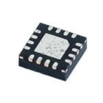
| 供应商器件封装 | 16-QFN(3x3) |
| 共模抑制比—最小值 | 90 dB |
| 其它名称 | 296-19324-6 |
| 制造商产品页 | http://www.ti.com/general/docs/suppproductinfo.tsp?distId=10&orderablePartNumber=THS4508RGTT |
| 包装 | Digi-Reel® |
| 单位重量 | 24.100 mg |
| 压摆率 | 6400 V/µs |
| 商标 | Texas Instruments |
| 增益带宽生成 | 3000 MHz |
| 增益带宽积 | 3GHz |
| 安装类型 | 表面贴装 |
| 安装风格 | SMD/SMT |
| 封装 | Reel |
| 封装/外壳 | 16-VFQFN 裸露焊盘 |
| 封装/箱体 | VQFN-16 |
| 工作温度 | -40°C ~ 85°C |
| 工作电源电压 | 5.25 V |
| 工厂包装数量 | 250 |
| 放大器类型 | 差分 |
| 最大工作温度 | + 85 C |
| 最小工作温度 | - 40 C |
| 标准包装 | 1 |
| 电压-电源,单/双 (±) | 3.75 V ~ 5.25 V |
| 电压-输入失调 | 1mV |
| 电流-电源 | 39.2mA |
| 电流-输入偏置 | 8µA |
| 电流-输出/通道 | 96mA |
| 电源电压-最大 | 5.25 V |
| 电源电压-最小 | 3.75 V |
| 电源电流 | 42.5 mA |
| 电路数 | 1 |
| 系列 | THS4508 |
| 输入电压范围—最大 | Positive Rail - 2.7 V (typ) |
| 输入补偿电压 | 4 mV |
| 输出电流—典型值 | 440 mA |
| 输出类型 | 差分 |
| 通道数量 | 1 Channel |
| 配用 | /product-detail/zh/THS4508EVM/296-21085-ND/1216691/product-detail/zh/THS4511EVM/296-21086-ND/1216692/product-detail/zh/THS4513EVM/296-21087-ND/1216693/product-detail/zh/THS4520EVM/296-31387-ND/1674029 |


.jpg)


- 商务部:美国ITC正式对集成电路等产品启动337调查
- 曝三星4nm工艺存在良率问题 高通将骁龙8 Gen1或转产台积电
- 太阳诱电将投资9.5亿元在常州建新厂生产MLCC 预计2023年完工
- 英特尔发布欧洲新工厂建设计划 深化IDM 2.0 战略
- 台积电先进制程称霸业界 有大客户加持明年业绩稳了
- 达到5530亿美元!SIA预计今年全球半导体销售额将创下新高
- 英特尔拟将自动驾驶子公司Mobileye上市 估值或超500亿美元
- 三星加码芯片和SET,合并消费电子和移动部门,撤换高东真等 CEO
- 三星电子宣布重大人事变动 还合并消费电子和移动部门
- 海关总署:前11个月进口集成电路产品价值2.52万亿元 增长14.8%


PDF Datasheet 数据手册内容提取
THS4508 www.ti.com.................................................................................................................................... SLAS459E–SEPTEMBER2005–REVISEDSEPTEMBER2008 WIDEBAND, LOW NOISE, LOW DISTORTION FULLY DIFFERENTIAL AMPLIFIER FEATURES To allow for dc coupling to analog-to-digital 1 • FullyDifferentialArchitecture converters (ADCs), its unique output common-mode control circuit maintains the output common-mode • Common-ModeInputRangeIncludesthe voltage within 5-mV offset (typical) from the set NegativeRail voltage, when set within 0.5 V of mid-supply. The • MinimumGainof2V/V(6dB) common-mode set point is set to mid-supply by • Bandwidth:2GHz internal circuitry, which may be over-driven from an externalsource. • SlewRate:6400V/m s The THS4508 is a high-performance amplifier that • 1%SettlingTime:2ns has been optimized for use in high performance, 5-V • HD2:–72dBcat100MHz single-supply data acquisition systems. The output • HD :–79dBcat100MHz has been optimized for best performance with its 3 • OIP :78dBmat70MHz common-mode voltages set to mid-supply, and the 2 input has been optimized for best performance with • OIP3:42dBmat70MHz its common-mode voltage set to 0.7 V. High • InputVoltageNoise:2.3nV/√Hz(f>10MHz) performance at a low power-supply voltage is ideal • NoiseFigure:19.2dB(G=10dB) for high-performance, single-supply 5-V data-acquisition systems with a minimum parts count. • OutputCommon-ModeControl The combined performance of the THS4508 in a gain • 5-VPowerSupplyCurrent:39.2mA of 10-dB driving the ADS5500 ADC, sampling at 125 • Power-DownCapability:0.65mA MSPS, is 82-dBc SFDR, and 68.3-dBc SNR with a –1-dBFSsignalat70MHz. APPLICATIONS The THS4508 is offered in a quad 16-pin leadless • 5-VData-AcquisitionSystems QFN package (RGT), and is characterized for • HighLinearityADCAmplifier operation over the full industrial temperature range from–40°Cto+85°C. • WirelessCommunication • MedicalImaging • TestandMeasurement RS= 75W VIN 175W 348W DESCRIPTION VSignal 130W VS+= 5 V RO The THS4508 is a wideband, fully-differential VOUT- operational amplifier designed for single-supply 5-V 175W THS4508 RO data acquisition systems. It has very low noise at 2.3 VCM VOUT+ nV/√Hz, and extremely low harmonic distortion of –72 75W 130W VS- dBc HD and –79 dBc HD at 100 MHz with 2 V , 2 3 PP G = 10 dB, and 1-kΩ load. Slew rate is very high at 348W 6400 Vm s, and with settling time of 2 ns to 1% (2 V Figure1.VideoBuffer step), it is ideal for pulsed applications. It is designed for minimum gain of 6 dB, but is optimized for gain of 10dB. 1 Pleasebeawarethatanimportantnoticeconcerningavailability,standardwarranty,anduseincriticalapplicationsofTexas Instrumentssemiconductorproductsanddisclaimerstheretoappearsattheendofthisdatasheet. PRODUCTIONDATAinformationiscurrentasofpublicationdate. Copyright©2005–2008,TexasInstrumentsIncorporated Products conform to specifications per the terms of the Texas Instruments standard warranty. Production processing does not necessarilyincludetestingofallparameters.
THS4508 SLAS459E–SEPTEMBER2005–REVISEDSEPTEMBER2008.................................................................................................................................... www.ti.com This integrated circuit can be damaged by ESD. Texas Instruments recommends that all integrated circuits be handled with appropriateprecautions.Failuretoobserveproperhandlingandinstallationprocedurescancausedamage. ESDdamagecanrangefromsubtleperformancedegradationtocompletedevicefailure.Precisionintegratedcircuitsmaybemore susceptibletodamagebecauseverysmallparametricchangescouldcausethedevicenottomeetitspublishedspecifications. ABSOLUTE MAXIMUM RATINGS(1) Overoperatingfree-airtemperaturerange(unlessotherwisenoted). UNIT V Supplyvoltage V toV 5.5V SS S– S+ V Inputvoltage ±V I S V Differentialinputvoltage 4V ID I Outputcurrent 200mA O Continuouspowerdissipation SeeDissipationRatingTable T Maximumjunctiontemperature(2) +150°C J T Maximumjunctiontemperature,continuousoperation,longtermreliability(3) +125°C J T Operatingfree-airtemperaturerange –40°Cto+85°C A T Storagetemperaturerange –65°Cto+150°C stg HBM 2000V ESDratings CDM 1500V MM 100V (1) Stressesabovetheseratingsmaycausepermanentdamage.Exposuretoabsolutemaximumconditionsforextendedperiodsmay degradedevicereliability.Thesearestressratingsonly,andfunctionaloperationofthedeviceattheseoranyotherconditionsbeyond thosespecifiedisnotimplied. (2) Theabsolutemaximumtemperatureunderanyconditionislimitedbytheconstraintsofthesiliconprocess. (3) Themaximumjunctiontemperatureforcontinuousoperationislimitedbythepackageconstraints.Operationabovethistemperature mayresultinreducedreliabilityand/orlifetimeofthedevice.TheTHS4508incorporatesa(QFN)exposedthermalpadontheunderside ofthechip.Thisactsasaheatsinkandmustbeconnectedtoathermallydissipativeplaneforproperpowerdissipation.Failuretodoso mayresultinexceedingthemaximumjunctiontemperaturewhichcouldpermanentlydamagethedevice.SeeTItechnicalbrief SLMA002andSLMA004formoreinformationaboututilizingtheQFNthermallyenhancedpackage. DISSIPATION RATINGS TABLE (PER PACKAGE) POWERRATING PACKAGE q q JC JA T ≤25°C T =85°C A A RGT(16) 2.4°C/W 39.5°C/W 2.3W 225mW ORDERINGINFORMATION(1) SPECIFIED PACKAGE- PACKAGE TEMPERATURE PACKAGE ORDERING TRANSPORTMEDIA, PRODUCT LEAD DESIGNATOR RANGE MARKING NUMBER QUANTITY THS4508RGTT TapeandReel,250 THS4508 QFN-16 RGT –40°Cto+85°C THS4508 THS4508RGTR TapeandReel,3000 (1) Forthemostcurrentpackageandorderinginformation,seethePackageOptionAddendumattheendofthisdocument,orseetheTI Websiteatwww.ti.com. 2 SubmitDocumentationFeedback Copyright©2005–2008,TexasInstrumentsIncorporated ProductFolderLink(s):THS4508
THS4508 www.ti.com.................................................................................................................................... SLAS459E–SEPTEMBER2005–REVISEDSEPTEMBER2008 DEVICE INFORMATION THS4508 (RGTPACKAGE) (TOPVIEW) V S- 16 15 14 13 NC 1 12 PD VIN- 2 11 VIN+ VOUT+ 3 10 VOUT- CM 4 9 CM 5 6 7 8 V S+ TERMINALFUNCTIONS TERMINAL (RGTPACKAGE) DESCRIPTION NO. NAME 1 NC Nointernalconnection 2 V Invertingamplifierinput IN– 3 V Noninvertingamplifieroutput OUT+ 4,9 CM Common-modevoltageinput 5–8 V Positiveamplifierpower-supplyinput S+ 10 V Invertingamplifieroutput OUT– 11 V Noninvertingamplifierinput IN+ 12 PD Power-down,PD=logiclowputspartintolow-powermode,PD=logichighoropenfornormaloperation 13–16 V Negativeamplifierpower-supplyinput S– Copyright©2005–2008,TexasInstrumentsIncorporated SubmitDocumentationFeedback 3 ProductFolderLink(s):THS4508
THS4508 SLAS459E–SEPTEMBER2005–REVISEDSEPTEMBER2008.................................................................................................................................... www.ti.com ELECTRICAL CHARACTERISTICS; V – V = 5 V: S+ S– Testconditionsunlessotherwisenoted:V =5V,V =0V,G=10dB,CM=open,V =2V ,R =349Ω,R =200Ω S+ S– O PP F L Differential,T=+25°CSingle-EndedInput,DifferentialOutput,InputReferencedtoGround,andOutputReferencedto Mid-supply. TEST PARAMETER TESTCONDITIONS MIN TYP MAX UNITS LEVEL(1) ACPERFORMANCE(seeFigure44) G=6dB,VO=100mVPP 2 GHz G=10dB,VO=100mVPP 1.7 GHz Small-SignalBandwidth G=14dB,VO=100mVPP 600 MHz G=20dB,VO=100mVPP 300 MHz Gain-BandwidthProduct G=20dB 3 GHz Bandwidthfor0.1dBflatness G=10dB,VO=2VPP 400 MHz Large-SignalBandwidth G=10dB,VO=2VPP 1.5 GHz SlewRate(Differential) 6400 V/m s RiseTime 0.5 ns FallTime VO=2-VStep 0.5 ns SettlingTimeto1% 2 ns SettlingTimeto0.1% 12 m s f=10MHz –104 2nd-OrderHarmonicDistortion f=50MHz –82 f=100MHz –69 dBc f=10MHz –105 C 3rd-OrderHarmonicDistortion f=50MHz –92 f=100MHz –81 fC=70MHz –78 2nd-OrderIntermodulationDistortion 200-kHztonespacing, fC=140MHz –64 dBc RL=499Ω fC=70MHz –95 3rd-OrderIntermodulationDistortion fC=140MHz –78 fC=70MHz 78 2nd-OrderOutputInterceptPoint 200-kHztonespacing, fC=140MHz 58 dBm RL=100Ω fC=70MHz 42 3rd-OrderOutputInterceptPoint fC=140MHz 35 1-dBCompressionPoint(2) fC=70MHz 12.2 dBm fC=140MHz 10.8 NoiseFigure 50-Ωsystem,10MHz 19.2 dB InputVoltageNoise f>10MHz 2.3 nV/√Hz InputCurrentNoise f>10MHz 2.9 pA/√Hz DCPERFORMANCE Open-LoopVoltageGain(AOL) 68 dB C TA=+25°C 1 4 InputOffsetVoltage mV A TA=–40°Cto+85°C 1 5 AverageOffsetVoltageDrift 2.3 µV/°C B InputBiasCurrent TA=+25°C 1.75 8 15.5 m A A TA=–40°Cto+85°C 8 18.5 AverageBiasCurrentDrift 20 nA/°C B InputOffsetCurrent TA=+25°C 0.5 3.6 m A A TA=–40°Cto+85°C 0.5 7 AverageOffsetCurrentDrift 7 nA/°C B (1) Testlevels:(A)100%testedat25°C.Overtemperaturelimitsbycharacterizationandsimulation.(B)Limitssetbycharacterizationand simulation.(C)Typicalvalueonlyforinformation. (2) The1-dBcompressionpointismeasuredattheloadwith50-Ωdoubletermination.Add3dBtorefertoamplifieroutput. 4 SubmitDocumentationFeedback Copyright©2005–2008,TexasInstrumentsIncorporated ProductFolderLink(s):THS4508
THS4508 www.ti.com.................................................................................................................................... SLAS459E–SEPTEMBER2005–REVISEDSEPTEMBER2008 ELECTRICAL CHARACTERISTICS; V – V = 5 V: (continued) S+ S– Testconditionsunlessotherwisenoted:V =5V,V =0V,G=10dB,CM=open,V =2V ,R =349Ω,R =200Ω S+ S– O PP F L Differential,T=+25°CSingle-EndedInput,DifferentialOutput,InputReferencedtoGround,andOutputReferencedto Mid-supply. TEST PARAMETER TESTCONDITIONS MIN TYP MAX UNITS LEVEL(1) INPUT Common-ModeInputRangeHigh 2.3 V B Common-ModeInputRangeLow –0.3 Common-ModeRejectionRatio 90 dB B 18.2|| DifferentialInputImpedance MΩ||pF C 2.2 Common-ModeInputImpedance 3.8||2.5 MΩ||pF C OUTPUT TA=+25°C 3.7 3.8 MaximumOutputVoltageHigh TA=–40°Cto 3.6 3.8 V Eachoutputwith100Ω +85°C A tomid-supply TA=+25°C 1.2 1.3 MinimumOutputVoltageLow TA=–40°Cto 1.2 1.4 +85°C TA=+25°C 4.8 5.2 DifferentialOutputVoltageSwing V A TA=–40°Cto+85°C 4.4 5.2 DifferentialOutputCurrentDrive RL=10Ω 96 mA C OutputBalanceError VO=100mV,f=1MHz –43 dB C Closed-LoopOutputImpedance f=1MHz 0.3 Ω C OUTPUTCOMMON-MODEVOLTAGECONTROL Small-SignalBandwidth 700 MHz SlewRate 110 V/m s Gain 1 V/V OutputCommon-ModeOffsetfromCMinput 1.25V<CM<3.5V 5 mV CMInputBiasCurrent 1.25V<CM<3.5V ±40 m A C 1.25to CMInputVoltageRange V 3.75 CMInputImpedance 32||1.5 kΩ||pF CMDefaultVoltage 2.5 V POWERSUPPLY SpecifiedOperatingVoltage 3.75(3) 5 5.25 V C MaximumQuiescentCurrent TA=+25°C 39.2 42.5 TA=–40°Cto+85°C 39.2 43.5 mA A MinimumQuiescentCurrent TA=+25°C 35.9 39.2 TA=–40°Cto+85°C 35 39.2 Power-SupplyRejection(±PSRR) Todifferentialoutput 90 dB C POWER-DOWN ReferencedtoVS– EnableVoltageThreshold Deviceassuredonabove2.1V >2.1 V C DisableVoltageThreshold Deviceassuredoffbelow0.7V <0.7 TA=+25°C 0.65 0.9 Power-DownQuiescentCurrent mA A TA=–40°Cto+85°C 0.65 1 InputBiasCurrent PD=VS– 100 m A InputImpedance 50||2 kΩ ||pF C Turn-onTimeDelay Measuredtooutputon 55 ns Turn-offTimeDelay Measuredtooutputoff 10 m s (3) SeetheApplicationInformationsectionofthisdatasheetfordeviceoperationwithfullsupplyvoltageslessthan5V. Copyright©2005–2008,TexasInstrumentsIncorporated SubmitDocumentationFeedback 5 ProductFolderLink(s):THS4508
THS4508 SLAS459E–SEPTEMBER2005–REVISEDSEPTEMBER2008.................................................................................................................................... www.ti.com TYPICAL CHARACTERISTICS TYPICAL AC PERFORMANCE: V – V = 5 V S+ S– Testconditionsunlessotherwisenoted:V =5V,V =0V,G=10dB,CM=open,V =2V ,R =349Ω,R =200Ω S+ S– O PP F L Differential,Single-EndedInput,InputReferencedtoGroundandOutputReferencedtoMidrail Small-SignalFrequencyResponse Figure2 LargeSignalFrequencyResponse Figure3 HD ,G=6dB,V =2V vsFrequency Figure4 2 OD PP HD ,G=6dB,V =2V vsFrequency Figure5 3 OD PP HD ,G=10dB,V =2V vsFrequency Figure6 2 OD PP HD ,G=10dB,V =2V vsFrequency Figure7 3 OD PP Harmonic HD2,G=14dB,VOD=2VPP vsFrequency Figure8 Distortion HD ,G=14dB,V =2V vsFrequency Figure9 3 OD PP HD ,G=10dB vsOutputvoltage Figure10 2 HD ,G=10dB vsOutputvoltage Figure11 3 HD ,G=10dB vsCMinputvoltage Figure12 2 HD ,G=10dB vsCMinputvoltage Figure13 3 IMD ,G=6dB,V =2V vsFrequency Figure14 2 OD PP IMD ,G=6dB,V =2V vsFrequency Figure15 3 OD PP Intermodulation IMD2,G=10dB,VOD=2VPP vsFrequency Figure16 Distortion IMD ,G=10dB,V =2V vsFrequency Figure17 3 OD PP IMD ,G=14dB,V =2V vsFrequency Figure18 2 OD PP IMD ,G=14dB,V =2V vsFrequency Figure19 3 OD PP OIP vsFrequency Figure20 2 OutputInterceptPoint OIP vsFrequency Figure21 3 S-Parameters vsFrequency Figure22 TransitionRate vsOutputVoltage Figure23 TransientResponse Figure24 SettlingTime Figure25 0.1dBFlatness Figure26 RejectionRatio vsFrequency Figure27 OutputImpedance vsFrequency Figure28 OverdriveRecovery Figure29 OutputVoltageSwing vsLoadResistance Figure30 Turn-OffTime Figure31 Turn-OnTime Figure32 InputOffsetVoltage vsInputCommon-ModeVoltage Figure33 OpenLoopGain vsFrequency Figure34 InputReferredNoise vsFrequency Figure35 NoiseFigure vsFrequency Figure36 QuiescentCurrent vsSupplyVoltage Figure37 OutputBalanceError vsFrequency Figure38 CMInputImpedance vsFrequency Figure39 CMSmall-SignalFrequencyResponse Figure40 CMInputBiasCurrent vsCMInputVoltage Figure41 DifferentialOutputOffsetVoltage vsCMInputVoltage Figure42 OutputCommon-ModeOffset vsCMInputVoltage Figure43 6 SubmitDocumentationFeedback Copyright©2005–2008,TexasInstrumentsIncorporated ProductFolderLink(s):THS4508
THS4508 www.ti.com.................................................................................................................................... SLAS459E–SEPTEMBER2005–REVISEDSEPTEMBER2008 TYPICALACPERFORMANCE:V –V =5V S+ S– Testconditionsunlessotherwisenoted:V =5V,V =0V,G=10dB,CM=open,V =2V ,R =349Ω,R =200Ω S+ S– O PP F L Differential,Single-EndedInput,InputReferencedtoGroundandOutputReferencedtoMidrail SMALL-SIGNALFREQUENCYRESPONSE LARGE-SIGNALFREQUENCYRESPONSE 22 22 G = 20 dB G = 20 dB 20 20 18 18 B B d d n - 16 G = 14 dB n - 16 G = 14 dB ai 14 ai 14 G G al 12 al 12 n G = 10 dB n G = 10 dB g g Si 10 Si 10 mall 8 G = 6 dB mall 8 G = 6 dB S S 6 6 4 4 2 VO= 100 mVPP 2 VOD= 2 VPP 0 0 100 k 1 M 10 M 100 M 1 G 10 G 100 k 1 M 10 M 100 M 1 G 10 G f - Frequency - Hz f - Frequency - Hz Figure2. Figure3. HD vsFREQUENCY HD vsFREQUENCY 2 3 -50 -60 G = 6 dB, G = 6 dB, -60 VOD= 2 VPP -70 VOD= 2 VPP -70 -80 HD- dBc2 --8900 RL= R10L0=W 200W RL= 1 kW HD- dBc3 -90 R = 100WRL= 499W -100 L -100 -110 R = 200W -110 R = 1 kW L L R = 499W -120 L -120 1 M 10 M 100 M 1 G 1 M 10 M 100 M 1 G f - Frequency - Hz f - Frequency - Hz Figure4. Figure5. Copyright©2005–2008,TexasInstrumentsIncorporated SubmitDocumentationFeedback 7 ProductFolderLink(s):THS4508
THS4508 SLAS459E–SEPTEMBER2005–REVISEDSEPTEMBER2008.................................................................................................................................... www.ti.com Testconditionsunlessotherwisenoted:V =5V,V =0V,G=10dB,CM=open,V =2V ,R =349Ω,R =200Ω S+ S– O PP F L Differential,Single-EndedInput,InputReferencedtoGroundandOutputReferencedtoMidrail HD vsFREQUENCY HD vsFREQUENCY 2 3 -60 -60 G = 10 dB, G = 10 dB, -70 VOD= 2 VPP -70 VOD= 2 VPP -80 -80 c - dBc -90 RL= 100W - dB3 -90 RL= 1 kW D2 RL= 200W HD RL= 100W H -100 -100 R = 200W L -110 RL= 499W -110 R = 499W R = 1 kW L L -120 -120 1 M 10 M 100 M 1 G 1 M 10 M 100 M 1 G f - Frequency - Hz f - Frequency - Hz Figure6. Figure7. HD vsFREQUENCY HD vsFREQUENCY 2 3 -50 -60 G = 14 dB, G = 14 dB, V = 2 V V = 2 V -60 OD PP OD PP -70 -70 R = 100W -80 L -90 R = 1 kW L R = 200W L c c B - dB -90 - d3 -80 RL= 499W 2 D HD -100 RL= 499W H RL= 100W -100 -110 R = 200W R = 1 kW L L -120 -110 1 M 10 M 100 M 1 G 1 M 10 M 100 M 1 G f - Frequency - Hz f - Frequency - Hz Figure8. Figure9. 8 SubmitDocumentationFeedback Copyright©2005–2008,TexasInstrumentsIncorporated ProductFolderLink(s):THS4508
THS4508 www.ti.com.................................................................................................................................... SLAS459E–SEPTEMBER2005–REVISEDSEPTEMBER2008 Testconditionsunlessotherwisenoted:V =5V,V =0V,G=10dB,CM=open,V =2V ,R =349Ω,R =200Ω S+ S– O PP F L Differential,Single-EndedInput,InputReferencedtoGroundandOutputReferencedtoMidrail HD vsOUTPUTVOLTAGE HD vsOUTPUTVOLTAGE 2 3 -40 -40 G = 10 dB, f = 150 MHz G = 10 dB, f = 150 MHz -50 VOD= 2 VPP -50 VOD= 2 VPP f = 100 MHz f = 100 MHz -60 -60 f = 64 MHz -70 f = 64 MHz -70 c f = 32 MHz B - dBc -80 f = 32 MHz - Dd3 -80 D2 -90 H -90 H f = 8 MHz -100 -100 f = 16 MHz f = 16 MHz -110 -110 f = 8 MHz -120 -120 0 1 2 3 4 5 0 1 2 3 4 5 VO- Output Voltage -VPP VO- Output Voltage -VPP Figure10. Figure11. HD vsCMOUTPUTVOLTAGE HD vsCMOUTPUTVOLTAGE 2 3 10 0 V = 1.2 V to 3.8 V V = 1.2 V to 3.8 V CM CM V = 2 V -10 VOD= 2 VPP 150 MHz -20 OD PP 150 MHz -30 100 MHz -40 Bc -50 Bc 100 MHz D- d2 -70 - Dd3 -60 H 64 MHz H -80 64 MHz -90 -100 16 MHz -110 1 MHz 1 MHz 4 MHz 16 MHz 4 MHz -120 -130 1.2 1.6 2 2.4 2.8 3.2 3.6 3.8 1.2 1.6 2 2.4 2.8 3.2 3.6 3.8 CM - Common Mode Output Voltage - V CM - Common Mode Output Voltage - V Figure12. Figure13. Copyright©2005–2008,TexasInstrumentsIncorporated SubmitDocumentationFeedback 9 ProductFolderLink(s):THS4508
THS4508 SLAS459E–SEPTEMBER2005–REVISEDSEPTEMBER2008.................................................................................................................................... www.ti.com Testconditionsunlessotherwisenoted:V =5V,V =0V,G=10dB,CM=open,V =2V ,R =349Ω,R =200Ω S+ S– O PP F L Differential,Single-EndedInput,InputReferencedtoGroundandOutputReferencedtoMidrail IMD vsFREQUENCY IMD vsFREQUENCY 2 3 −30 -50 G = 6 dB, G = 6 dB, −40 VOD= 2 VPPEnvelope, VOD= 2 VPPEnvelope, 200 kHz Tone Spacing R = 200W -60 200 kHz Tone Spacing L −50 RL= 100W RL= 100W -70 dBc −60 Bc RL= 200W MD−2 −70 MD- d3 -80 I I -90 −80 RL= 499W RL= 1 kW −90 RL= 1 kW -100 R = 499W L −100 -110 0 50 100 150 200 0 50 100 150 200 f−Frequency−MHz f - Frequency - MHz Figure14. Figure15. IMD vsFREQUENCY IMD vsFREQUENCY 2 3 -30 -60 G = 10 dB, G = 10 dB, -40 V20O0D k=H 2z VToPnPeE nSvpealcoipneg, RL= 100W -65 V20O0D k=H 2z VToPnPeE Snvpealcoipneg, RL= 100W RL= 200W -70 -50 -75 Bc -60 Bc RL= 200W D- d2 -70 MD- d3 -80 IM RL= 499W I -85 R = 1 kW L -80 R = 1 kW -90 L -90 -95 R = 499W L -100 -100 0 50 100 150 200 0 50 100 150 200 f - Frequency - MHz f - Frequency - MHz Figure16. Figure17. 10 SubmitDocumentationFeedback Copyright©2005–2008,TexasInstrumentsIncorporated ProductFolderLink(s):THS4508
THS4508 www.ti.com.................................................................................................................................... SLAS459E–SEPTEMBER2005–REVISEDSEPTEMBER2008 Testconditionsunlessotherwisenoted:V =5V,V =0V,G=10dB,CM=open,V =2V ,R =349Ω,R =200Ω S+ S– O PP F L Differential,Single-EndedInput,InputReferencedtoGroundandOutputReferencedtoMidrail IMD vsFREQUENCY IMD vsFREQUENCY 2 3 -40 -60 R = 100W RL= 100W -65 L -50 -70 RL= 200W RL= 200W -75 -60 Bc RL= 1 kW dBc -80 MD- d2 -70 RL= 499W IMD- 3 --8950 RL= 1 kW I -80 -95 G = 14 dB, -100 G = 14 dB, -90 V20O0D k=H 2z VToPnPeE Snpvaecloinpge, -105 RL= 499W V20O0D k=H 2z VToPnPeE nSvpealcoipneg, -100 -110 0 50 100 150 200 0 50 100 150 200 f - Frequency - MHz f - Frequency - MHz Figure18. Figure19. OIP vsFREQUENCY OIP vsFREQUENCY 2 3 90 50 G = 10 dB 85 80 45 G = 14 dB G = 10 dB 75 G = 6 dB m 70 m 40 OIP- dB2 6650 G = 6 dB OIP- dB3 35 G = 14 dB 55 50 RL= 100W, 30 RL= 100W, 45 VOD= 2 VPPEnvelope, VOD= 2 VPPEnvelope, 200 kHz Tone Spacing 200 kHz Tone Spacing 40 25 0 50 100 150 200 0 50 100 150 200 f - Frequency - MHz f - Frequency - MHz Figure20. Figure21. Copyright©2005–2008,TexasInstrumentsIncorporated SubmitDocumentationFeedback 11 ProductFolderLink(s):THS4508
THS4508 SLAS459E–SEPTEMBER2005–REVISEDSEPTEMBER2008.................................................................................................................................... www.ti.com Testconditionsunlessotherwisenoted:V =5V,V =0V,G=10dB,CM=open,V =2V ,R =349Ω,R =200Ω S+ S– O PP F L Differential,Single-EndedInput,InputReferencedtoGroundandOutputReferencedtoMidrail S-PARAMETERSvsFREQUENCY TRANSITIONRATEvsOUTPUTVOLTAGE 20 8000 10 Gain = 10 dB, Rising 7000 R = 200W 0 S21 L 20 % - 80% -10 s 6000 s - dB -20 S11 me - V/ 5000 Falling er -30 at met -40 n R 4000 s-Para --6500 S22 Transitio 23000000 -70 S12 -80 1000 -90 0 100 k 1 M 10 M 100 M 1 G 10 G 0 0.5 1 1.5 2 2.5 3 3.5 4 f - Frequency - Hz V - Output Voltage - V O Figure22. Figure23. TRANSIENTRESPONSE SETTLINGTIME 4 0.5 3.75 V = 2 V step e - V 3.5 0.3 OD ag 3.25 % ut Volt 2.753 Gain = 10 dB, alue - 0.1 utp 2.5 RL= 200W, al V O V = 2 V n erential 2.252 OD PP ent of Fi -0.1 Diff 1.75 erc -0.3 - 1.5 P D O 1.25 V 1 -0.5 t - Time - (250 psec/div) t - Time - 1 ns/div Figure24. Figure25. 0.1-dBFLATNESS REJECTIONRATIOvsFREQUENCY 10.5 100 10.4 90 V = 100 mV PSRR+ OD PP 80 10.3 10.2 dB 70 CMRR ain - dB 10.1 Ratio - 5600 G 10 n gnal 9.9 ectio 40 Si ej 30 9.8 R VCM = VS/ 2, 20 R = 200W L 9.7 10 9.6 0 100 k 1 M 10 M 100 M 1 G 10 k 100 k 1 M 10 M 100 M 1 G f - Frequency - Hz f - Frequency - Hz Figure26. Figure27. 12 SubmitDocumentationFeedback Copyright©2005–2008,TexasInstrumentsIncorporated ProductFolderLink(s):THS4508
THS4508 www.ti.com.................................................................................................................................... SLAS459E–SEPTEMBER2005–REVISEDSEPTEMBER2008 Testconditionsunlessotherwisenoted:V =5V,V =0V,G=10dB,CM=open,V =2V ,R =349Ω,R =200Ω S+ S– O PP F L Differential,Single-EndedInput,InputReferencedtoGroundandOutputReferencedtoMidrail OUTPUTIMPEDANCEvsFREQUENCY OVERDRIVERECOVERY 100 5.75 2 4.75 Input 1.5 W 3.75 - Output Impedance -O 101 - Output Voltage - V ---012021......272772555555 Output 00-10.5.5 V- Input Voltage - VI Z O Gain = 10 dB, V -3.25 RL= 200W -1 -4.25 0.1 -5.25 -1.5 100 k 1 M 10 M 100 M 1 G t - Time - 100 ns/div f - Frequency - Hz Figure28. Figure29. V SWINGvsLOADRESISTANCE TURN-OFFTIME OD 7 3.2 6.4 V g - 3 6 n 6 2.8 5.6 Swi 2.6 5.2 ge 5 V 2.4 Output 4.8 ut Volta 4 oltage - 12..822 434..46 nput - V - Differential OutpD 231 V- Output VO011001......4466821 GRLai=n 2=0 10P0WD d BIn,put 2202311......488226 Powerdown I O 0.2 0.4 V 0 0 0 10 100 1000 t - Time - (2.5ms/div) R - Load Resistance - kW L Figure30. Figure31. Copyright©2005–2008,TexasInstrumentsIncorporated SubmitDocumentationFeedback 13 ProductFolderLink(s):THS4508
THS4508 SLAS459E–SEPTEMBER2005–REVISEDSEPTEMBER2008.................................................................................................................................... www.ti.com Testconditionsunlessotherwisenoted:V =5V,V =0V,G=10dB,CM=open,V =2V ,R =349Ω,R =200Ω S+ S– O PP F L Differential,Single-EndedInput,InputReferencedtoGroundandOutputReferencedtoMidrail TURN-ONTIME INPUTOFFSETVOLTAGEvsCMINPUTVOLTAGE 3 6.4 10 2.8 PD Input 6 9 2.6 5.6 2.4 5.2 mV 8 - Output Voltage - V 111021......46882221 Output 24242334......448826 werdown Input - V nput Offset Voltage - 45637 VO 000...462 GRLai=n 2=0 100W dB, 011...826 Po V- IOS 2 1 0 0.4 -0.2 0 0 t - Time - (2.5ms/div) -0.5 0 0.5 1 1.5 2 2.5 3 V - Commom-Mode Input Voltage - V IC Figure32. Figure33. OPENLOOPGAINANDPHASEvsFREQUENCY INPUT-REFERREDNOISEvsFREQUENCY 90 50 100 80 p Gain−dB 45670000 Gain Phase −0−15000 hase−degrees Ö-NoisenVHz-ÖNoisepAHz 10 Open Loo 123000 −−210500 Open Loop P -VVoltage n-ICurrent n Vn In 0 −10 −250 1 1 100 10 k 1 M 100 M 10 G 10k 100k 1M 10M f−Frequency−Hz f-Frequency-Hz Figure34. Figure35. 14 SubmitDocumentationFeedback Copyright©2005–2008,TexasInstrumentsIncorporated ProductFolderLink(s):THS4508
THS4508 www.ti.com.................................................................................................................................... SLAS459E–SEPTEMBER2005–REVISEDSEPTEMBER2008 Testconditionsunlessotherwisenoted:V =5V,V =0V,G=10dB,CM=open,V =2V ,R =349Ω,R =200Ω S+ S– O PP F L Differential,Single-EndedInput,InputReferencedtoGroundandOutputReferencedtoMidrail NOISEFIGUREvsFREQUENCY QUIESCENTCURRENTvsSUPPLYVOLTAGE 22 44 T = 25oC 21 G = 6 dB 42 A 20 A TA= 85oC m 40 ure - dB 1189 G = 10 dB urrent - 38 se Fig 1167 G = 14 dB 50-WSystem cent C 36 TA= -40oC Noi 15 uies 34 14 G = 20 dB - QQ 32 I 13 30 12 28 0 20 40 60 80 100 120 140 160 180 200 3.75 4 4.25 4.5 4.75 5 5.25 f - Frequency - MHz VS- Supply Voltage - V Figure36. Figure37. OUTPUTBALANCEERRORvsFREQUENCY CMINPUTIMPEDANCEvsFREQUENCY 0 100 k Gain = 10 dB, ut Balance Error - dB ----21430000 VRVCOLOD=M =20 =20 VVWSP,P/ 2, WMode Input Impedance - 101 kk Outp -50 mon- 100 m o C -60 10 100 k 1 M 10 M 100 M 1 G 100 k 1 M 10 M 100 M 1 G f - Frequency - Hz f - Frequency - Hz Figure38. Figure39. Copyright©2005–2008,TexasInstrumentsIncorporated SubmitDocumentationFeedback 15 ProductFolderLink(s):THS4508
THS4508 SLAS459E–SEPTEMBER2005–REVISEDSEPTEMBER2008.................................................................................................................................... www.ti.com Testconditionsunlessotherwisenoted:V =5V,V =0V,G=10dB,CM=open,V =2V ,R =349Ω,R =200Ω S+ S– O PP F L Differential,Single-EndedInput,InputReferencedtoGroundandOutputReferencedtoMidrail CMSMALL-SIGNALFREQUENCYRESPONSE CMBIASCURRENTvsCMINPUTVOLTAGE 5 200 A 0 m nt - 100 e -5 urr C s 0 dB -10 Bia Gain - -15 e Input- -100 d -20 Mo n- o -200 -25 m m o C -30 -300 100 k 1 M 10 M 100 M 1 G 0 0.5 1 1.5 2 2.5 3 3.5 4 4.5 5 f - Frequency - Hz V - Common-Mode Input Voltage - V IC Figure40. Figure41. V OFFSETVOLTAGEvsCMINPUTVOLTAGE V OFFSETVOLTAGEvsCMINPUTVOLTAGE OD OC 5 V m 50 Offset Voltage - mV 432 ut Offset Voltage - 43120000 ut utp 0 p O ut e -10 O 1 d ntial n-Mo -20 ere 0 mo -30 Diff -1 - Com -40 0 0.5 1 1.5 2 2.5 3 3.5 4 4.5 5 C -50 V - Common-Mode Input Voltage - V VO 0 0.5 1 1.5 2 2.5 3 3.5 4 4.5 5 IC V - Common-Mode Input Voltage - V IC Figure42. Figure43. 16 SubmitDocumentationFeedback Copyright©2005–2008,TexasInstrumentsIncorporated ProductFolderLink(s):THS4508
THS4508 www.ti.com.................................................................................................................................... SLAS459E–SEPTEMBER2005–REVISEDSEPTEMBER2008 TEST CIRCUITS The output is probed using a high-impedance differential probe across the 100-Ω resistor. The gain The THS4508 is tested with the following test circuits is referred to the amplifier output by adding back the built on the EVM. For simplicity, the power supply 6-dBlossduetothevoltagedividerontheoutput. decoupling is not shown—see the layout in the Application Information section for recommendations. From VIN RG RF Depending on the test conditions, component values 50W Source 5 V are changed per the following tables, or as otherwise RIT noted. The signal generators used are ac-coupled 49.9W Output Measured 50-Ω sources, and a 0.22-m F capacitor and a 49.9-Ω RG THS4508 49.9W 100W HImepree dWainthc eHigh resistor to ground are inserted across RIT on the Differential Probe alternateinputtobalancethecircuit. 0.22mF RIT CM Open 49.9W 0.22mF Table1.GainComponentValues RF GAIN R R R F G IT Figure44.FrequencyResponseTestCircuit 6dB 348Ω 165Ω 61.9Ω 10dB 348Ω 100Ω 69.8Ω Distortionand1dbCompression 14dB 348Ω 56.2Ω 88.7Ω 20dB 348Ω 16.5Ω 287Ω The circuit shown in Figure 45 is used to measure harmonic distortion, intermodulation distortion, and Note the gain setting includes 50-Ω source 1-dbcompressionpointoftheamplifier. impedance. Components are chosen to achieve gainand50-Ωinputtermination. A signal generator is used as the signal source and theoutputismeasuredwitha spectrum analyzer. The Table2.LoadComponentValues output impedance of the signal generator is 50 Ω. RIT and R are chosen to impedance-match to 50 Ω, and G RL RO ROT Atten. to maintain the proper gain. To balance the amplifier, 100Ω 25Ω Open 6dB a 0.22-m F capacitor and 49.9-Ω resistor to ground are 200Ω 86.6Ω 69.8Ω 16.8dB insertedacrossRITonthealternateinput. 499Ω 237Ω 56.2Ω 25.5dB A low-pass filter is inserted in series with the input to 1kΩ 487Ω 52.3Ω 31.8dB reduce harmonics generated at the signal source. The level of the fundamental is measured, then a Note the total load includes 50-Ω termination by high-pass filter is inserted at the output to reduce the the test equipment. Components are chosen to fundamental so that it does not generate distortion in achieve load and 50-Ω line termination through a theinputofthespectrumanalyzer. 1:1transformer. The transformer used in the output to convert the Due to the voltage divider on the output formed by signal from differential to single-ended is an the load component values, the amplifier output is ADT1-1WT. It limits the frequency response of the attenuated. The column Atten in Table 2 shows the circuit so that measurements cannot be made below attenuation expected from the resistor divider. When approximately1MHz. using a transformer at the output as shown in Figure 45, the signal will see slightly more loss, and FromVIN RG RF thesenumberswillbeapproximate. 50W Source 5 V RIT FrequencyResponse RO 1:1 VOUTTo 50W Test ThecircuitshowninFigure44is used to measure the RG THS4508 RO ROT Equipment frequencyresponseofthecircuit. 0.22mF CM RIT Open A network analyzer is used as the signal source and 0.22mF 49.9W as the measurement device. The output impedance RF of the network analyzer is 50 Ω. R and R are IT G chosen to impedance match to 50 Ω, and to maintain Figure45.DistortionTestCircuit the proper gain. To balance the amplifier, a 0.22-m F capacitor and 49.9-Ω resistor to ground are inserted acrossR onthealternateinput. IT Copyright©2005–2008,TexasInstrumentsIncorporated SubmitDocumentationFeedback 17 ProductFolderLink(s):THS4508
THS4508 SLAS459E–SEPTEMBER2005–REVISEDSEPTEMBER2008.................................................................................................................................... www.ti.com The 1-dB compression point is measured with a at V or V with the input injected at V , R = OUT+ OUT– IN CM spectrum analyzer with 50-Ω double termination or 0 Ω and R = 49.9 Ω. The input impedance is CMT 100-Ω termination as shown in Table 2. The input measured with R = 49.9 Ω with R = open, and CM CMT power is increased until the output is 1 dB lower than calculated by measuring the voltage drop across R CM expected. The number reported in the table data is todeterminetheinputcurrent. the power delivered to the spectrum analyzer input. R R Add3dBtorefertotheamplifieroutput. G F 0.22mF 5 V R S-Parameter,SlewRate,TransientResponse, IT 49.9W SettlingTime,OutputImpedance,Overdrive, 49.9W V To OUT– 50-W OutputVoltage,andTurn-On/OffTime RG THS4508 49.9W Test VOUT+ Equipment Ts-hpearcaimrceutietrssh,oswlenwinraFteig,utrraen4s6ienist ruessepdontsoe,mseeatstluinreg 0.22mF RIT CM RCM V From IN time, output impedance, overdrive recovery, output 49.9W R 50-W CMT source voltage swing, and turn-on/turn-off times of the RF amplifier. For output impedance, the signal is injected at V with V left open and the drop across the Figure47.CMInputTestCircuit OUT IN 49.9 Ω resistor is used to calculate the impedance seenlookingintotheamplifieroutput. CMRRandPSRR Because S is measured single-ended at the load 21 ThecircuitshowninFigure48is used to measure the with 50-Ω double termination, add 12 dB to refer to CMRR and PSRR of V and V . The input is theamplifieroutputasadifferentialsignal. S+ S– switched appropriately to match the test being FromVIN RG RF performed. 50-W Source RIT 5 V VS+ 348W 49.9W PSRR+ 5 V VOUT+ To 50-W FromVIN 100W 49.9W Output RG THS4508 49.9W VOUT- TEeqsutipment So5u0rcWe CMRR 100W THS4508 49.9W 100W MHWeeitrahes Hurigehd 0.4292.9mFW RIT CM 0O.2p2emnF PSRR-VS- 69.8W CM 0O.2p2emnF IDPmrifopfeberedeannticael RF 348W Figure46.S-Parameter,SR,TransientResponse, Figure48.CMRRandPSRRTestCircuit SettlingTime,Z ,OverdriveRecovery,V O OUT Swing,andTurn-On/OffTestCircuit CMInput ThecircuitshowninFigure47is used to measure the frequency response and input impedance of the CM input. Frequency response is measured single-ended 18 SubmitDocumentationFeedback Copyright©2005–2008,TexasInstrumentsIncorporated ProductFolderLink(s):THS4508
THS4508 www.ti.com.................................................................................................................................... SLAS459E–SEPTEMBER2005–REVISEDSEPTEMBER2008 APPLICATION INFORMATION APPLICATIONS Single-Ended RG RF Input The following circuits show application information for 5 V Differential the THS4508. For simplicity, power-supply Output decoupling capacitors are not shown in these + – V diagrams. For more detail on the use and operation OUT– THS4508 of fully differential operational amplifiers, refer to RG – + application report Fully-Differential Amplifiers VOUT+ (SLOA054) , available for download at the TI web site. DifferentialInputtoDifferentialOutputAmplifier RF The THS4508 is a fully differential operational Figure50. Single-EndedInputtoDifferential amplifier, and can be used to amplify differential input OutputAmplifier signals to differential output signals. A basic block diagram of the circuit is shown in Figure 49 (CM input not shown). The gain of the circuit is set by R InputCommon-ModeVoltageRange F dividedbyR . G The input common-model voltage of a fully differential R operational amplifier is the voltage at the (+) and (–) F inputpinsoftheoperationalamplifier. Differential Differential Input 5 V Output It is important to not violate the input common-mode voltage range (V ) of the operational amplifier. ICR R Assuming the operational amplifier is in linear VIN+ G + – VOUT– operation the voltage across the input pins is only a THS4508 few millivolts at most. So finding the voltage at one VIN– RG – + VOUT+ ionfptuhtepoinpedreatteiornmainlaems pthliefieinr.put common-mode voltage Treating the negative input as a summing node, the voltageisgivenbyEquation1: æ R ö æ R ö V =çV ´ G ÷+çV ´ F ÷ RF IC çè OUT+ RG +RF ÷ø çè IN- RG +RF ÷ø (1) Figure49.DifferentialInputtoDifferentialOutput Amplifier To determine the V of the operational amplifier, the ICR voltage at the negative input is evaluated at the extremesofV . Depending on the source and load, input and output OUT+ termination can be accomplished by adding R and As the gain of the operational amplifier increases, the IT R . input common-mode voltage becomes closer and O closer to the input common-mode voltage of the Single-EndedInputtoDifferentialOutput source. Amplifier SettingtheOutputCommon-ModeVoltage The THS4508 can be used to amplify and convert single-ended input signals to differential output The output common-mode voltage is set by the signals. A basic block diagram of the circuit is shown voltage at the CM pin(s). The internal common-mode in Figure 50 (CM input not shown). The gain of the control circuit maintains the output common-mode circuitisagainsetbyRFdividedbyRG. voltage within 5-mV offset (typical) from the set voltage, when set within 0.5 V of mid-supply. If left unconnected, the common-mode set point is set to mid-supply by internal circuitry, which may be over-driven from an external source. Figure 51 is representative of the CM input. The internal CM circuit has about 700 MHz of –3-dB bandwidth, which Copyright©2005–2008,TexasInstrumentsIncorporated SubmitDocumentationFeedback 19 ProductFolderLink(s):THS4508
THS4508 SLAS459E–SEPTEMBER2005–REVISEDSEPTEMBER2008.................................................................................................................................... www.ti.com is required for best performance, but it is intended to be a dc-bias input pin. Bypass capacitors are RS RG RF recommended on this pin to reduce noise at the output. The external current required to overdrive the V RIT RPD VS+= 3.75 V to 5 V Signal internalresistordividerisgivenbyEquation2: R O 2V -(V -V ) VOUT- IEXT = CM 50kSW+ S- RG THS4508 RO VOUT+ (2) CM RS RIT RPD VS– where V is the voltage applied to the CM pin, and V CM CM V ranges from 3.75 V to 5 V, and V is 0 V S+ S– R (ground). F Figure52. THS4508DC-CoupledSingle-Source V S+ SupplyRangeFrom3.75Vto5VWithR Used PD ToSetV IC 50 kW I EXT Note that in Figure 52, the source is referenced to to internal CM ground as is the input termination resistor RIT. The CM circuit proper value of resistance to add can be calculated fromEquation3: 50 kW 1 RPD = é ù VS– 1 ê 1.6 ú 1 ê ú - Figure51. CMInputCircuit RF ê VS + - 1.6 ú RI êë 2 úû DeviceOperationwithSinglePowerSupplies Lessthan5V (3) whereR =R +R ||R . TheTHS4508isoptimizedtoworkinsystemsusing a I G S IT 5-V single supply, and the characterization data V is the power-supply voltage, R is the feedback S+ F presented in this data sheet were taken with 5-V resistance, R is the gain-setting resistance, R is the G S single-supply inputs. For ac-coupled systems or signal source resistance, and R is the termination IT dc-coupled systems operating with supplies less than resistance. 5 V and greater than 3.75 V, the amplifier input common-mode range is maximized by adding Table 3 is a modification of Table 1 to add the proper pull-down resistors at the device inputs. The values with RPD assuming VS+ = 3.75 V, a dc-coupled pull-down resistors provide additional loading at the 50-Ω source impedance, and setting the output input,andlowerthecommon-modevoltage that is fed common-modevoltagetomid-supply. back into the device input through resistor R . F Figure 52 shows the circuit configuration for this Table3.RPDValuesforVariousGains, V =3.75V,DC-CoupledSignalSource mode of operation where R is added to the S+ PD dc-coupled circuit to avoid violating the VICR of the Gain RF RG RIT RPD operational amplifier. Note R and R are added to S IT 6dB 348Ω 169Ω 64.9Ω 86.6Ω the alternate input from the signal input to balance 10dB 348Ω 102Ω 78.7Ω 110Ω the amplifier. One resistor that is equal to the combined value R = R + R || R can be placed at 14dB 348Ω 61.9Ω 115Ω 158Ω I G S IT thealternateinput. 20dB 348Ω 40.2Ω 221Ω 226Ω If the signal originates from an ac-coupled 50-Ω source (see Figure 53), the equivalent dc-source resistance is an open circuit and R = R + R . I G IT Table 4 is a modification of Table 1 to add the proper values with R assuming V = 3.75 V, an PD S+ ac-coupled 50-Ω source impedance, and setting the outputcommon-modevoltagetomid-supply. 20 SubmitDocumentationFeedback Copyright©2005–2008,TexasInstrumentsIncorporated ProductFolderLink(s):THS4508
THS4508 www.ti.com.................................................................................................................................... SLAS459E–SEPTEMBER2005–REVISEDSEPTEMBER2008 Table4.R ValuesforVariousGains, PD V =3.75V,AC-CoupledSignalSource 0.8 S+ Gain RF RG RIT RPD 0.6 6dB 348Ω 169Ω 64.9Ω 80.6Ω 0.4 10dB 348Ω 102Ω 78.7Ω 90.9Ω V 14dB 348Ω 61.9Ω 115Ω 90.9Ω ge - 0.2 a 20dB 348Ω 40.2Ω 221Ω 77.6Ω olt V 0 C RS RG RF -0.2 VSignal RIT RPD VS+= 3.75 V to 5 V -0.4 RO 0 5 10 15 20 VOUT- t - Time -ms RG THS4508 RO C CM VOUT+ Figure55.Y'SignalWSitighn3a-lLevelSyncandVideo RS RIT RPD VS- RF 1.5 V SFuigpuprley5R3a.nTgHeSF4ro5m0T8o3A.7SC5e-CtVVotuop5leVdWSiinthglRe-PSDoUusrceed utput - 1 IC O er 0.5 uff VideoBuffer B o 0 e d Figure 54 shows a possible application of the Vi THS4508 as a dc-coupled video buffer with a gain of - D -0.5 2. Figure 55 shows a plot of the Y' signal originating VO from a HDTV 720p video system. The input signal -1 includes a 3-level sync (minimum level at –0.3 V), 0 5 10 15 20 and the portion of the video signal with maximum t - Time -ms amplitude of 0.7 V. Although the buffer draws its Figure56.VideoBufferDifferentialOutputSignal power from a 5-V single-ended power supply, internal level shifters allow the buffer to support input signals which are as much as –0.3 V below ground. This THS4508+ADS5500CombinedPerformance allows maximum design flexibility while maintaining a The THS4508 is designed to be a high-performance minimum parts count. Figure 56 shows the differential drive amplifier for high-performance data converters output of the buffer. Note that the dc-coupled such as the ADS5500 14-bit 125-MSPS ADC. amplifier can introduce a dc offset on a signal applied Figure 57 shows a circuit combining the two devices, atitsinput and Figure 58 shows the combined SNR and SFDR Video performance versus frequency with –1 dBFS input Source signal level sampling at 125 MSPS. The THS4508 RS= 75W VIN 175W 348W amplifier circuit provides 10 dB of gain, and converts the single-ended input signal to a differential output VSignal 130W VS+= 5 V signal. The default common-mode output of the RO THS4508 (2.5 V) is not compatible with the required common-mode input of the ADS5500 (1.55 V), so 175W THS4508 RO VOD dc-blocking capacitors are added (0.22 µF). Note that VCM a biasing circuit (not shown in Figure 57) is needed to 75W 130W VS- provide the required common-mode, dc-input for the ADS5500. The 100-Ω resistors and 2.7-pF capacitor 348W between the THS4508 outputs and ADS5500 inputs along with the input capacitance of the ADS5500 limit Figure54.Single-SupplyVideoBuffer,Gain=2 the bandwidth of the signal to 115 MHz (–3 dB). For testing, a signal generator is used for the signal source. The generator is an ac-coupled 50-Ω source. A band-pass filter is inserted in series with the input to reduce harmonics and noise from the signal Copyright©2005–2008,TexasInstrumentsIncorporated SubmitDocumentationFeedback 21 ProductFolderLink(s):THS4508
THS4508 SLAS459E–SEPTEMBER2005–REVISEDSEPTEMBER2008.................................................................................................................................... www.ti.com source. Input termination is accomplished via the The 225-Ω resistors and 2.7-pF capacitor between 69.8-Ω resistor and 0.22-m F capacitor to ground in the THS4508 outputs and ADS5424 inputs (along conjunction with the input impedance of the amplifier with the input capacitance of the ADC) limit the circuit. A 0.22-m F capacitor and 49.9-Ω resistor is bandwidthofthesignaltoabout100MHz(–3dB). inserted to ground across the 69.8-Ω resistor and 0.22-m F capacitor on the alternate input to balance When the THS4508 is operated from a single power supply with V = 5 V and V = ground, the 2.5-V the circuit. Gain is a function of the source S+ S– output common-mode voltage is compatible with the impedance, termination, and 348-Ω feedback resistor. recommended value of the ADS5424 input See Table 1 for component values to set proper 50-Ω common-modevoltage(2.4V). terminationforothercommongains. V From VIN 100W 348W IN 100W 348W From 50-W 5s0o-uWrce 5 V source 69.8W 5 V 14-bit, 69.8W 0.22mF 100W A1I2N154+ M-bSitP,S 100 THS4508 222525WW 2.7pF 1AA0DI5NS+M5S4P24S 100W THS4508 2.7 pF AADINS5-50C0M AIN– VBG CM 49.9W 69.8W CM 0.22mF 100W 49.9W 69.8W 49.9W 0.22mF 0.22mF 0.1mF 348W 0.1mF 0.1mF 348W Figure59. THS4508+ADS5424Circuit Figure57. THS4508+ADS5500Circuit 95 95 SFDR 90 90 85 85 SFDR 80 80 75 75 SNR SNR 70 70 65 65 60 10 20 30 40 50 60 10 20 30 40 50 60 70 80 90 100 110 Input Frequency - MHz Input Frequency - MHz Figure60. THS4508+ADS5424SFDRandSNR Figure58. THS4508+ADS5500SFDRandSNR PerformancevsFrequency PerformanceversusFrequency THS4508+ADS5424CombinedPerformance Figure 59 shows the THS4508 driving the ADS5424 ADC, and Figure 60 shows the combined SNR and SFDR performance versus frequency with –1 dBFS inputsignallevelandsamplingat80MSPS. As before, the THS4508 amplifier provides 10 dB of gain, converts the single-ended input to differential, and sets the proper input common-mode voltage to the ADS5424. Input termination and circuit testing is the same as described above for the THS4508 + ADS5500circuit. 22 SubmitDocumentationFeedback Copyright©2005–2008,TexasInstrumentsIncorporated ProductFolderLink(s):THS4508
THS4508 www.ti.com.................................................................................................................................... SLAS459E–SEPTEMBER2005–REVISEDSEPTEMBER2008 LayoutRecommendations andL3. It is recommended to follow the layout of the external 8. A single-point connection to ground on L2 is components near the amplifier, ground plane recommended for the input termination resistors construction, and power routing of the EVM as R1 and R2. This should be applied to the input closelyaspossible.Generalguidelinesare: gainresistorsifterminationisnotused. 1. Signal routing should be direct and as short as 9. The THS4508 recommended printed circuit board possible into and out of the operational amplifier (PCB)footprintisshowninFigure61. circuit. 2. The feedback path should be short and direct 0.144 avoidingvias. 0.049 3. Ground or power planes should be removed from directly under the amplifier’s input and output 0.012 pins. Pin 1 0.0095 4. An output resistor is recommended on each output,asneartotheoutputpinaspossible. 0.015 5. Two 10-m F and two 0.1-m F power-supply 0.144 0.0195 0.0705 decoupling capacitors should be placed as near tothepower-supplypinsaspossible. 6. Two 0.1-m F capacitors should be placed between 0.032 0.010 the CM input pins and ground. This limits noise vias coupled into the pins. One each should be placed togroundnearpin4andpin9. 0.030 7. It is recommended to split the ground pane on 0.0245 layer 2 (L2) as shown below and to use a solid Top View ground on layer 3 (L3). A single-point connection should be used between each split section on L2 Figure61. QFNEtchandViaPattern Copyright©2005–2008,TexasInstrumentsIncorporated SubmitDocumentationFeedback 23 ProductFolderLink(s):THS4508
THS4508 SLAS459E–SEPTEMBER2005–REVISEDSEPTEMBER2008.................................................................................................................................... www.ti.com THS4508EVM Figure 62 is the THS4508 EVAL1 EVM schematic. Layers 1 through 4 of the PCB are shown in Figure 63 throughFigure66,andTable5liststhebillofmaterialfortheEVMassuppliedfromTI. GND VS+ J5 J6 VCC 10mF 10mF 0.1mF 0.1mF TP1 C3 C5 C12 C13 J8 R5 R1 348W VCC VCC J1 69.8W 6 8 R9 R3 12 5 7 open R12 C15 100W 2 PD 3 R7 T1 J3 C1 49.9W 0.22mF U1 11 - VO+ 86.6W R11 6 1 open J2 R4 4 + PwrPVadO1-0 86R.68W 69.8 W 54 3 oCp8en oCpe7n R2 100W Voc9m 14151613 R10 XFMR_ADT1-1WT opCe2n 69.8W R6 open J7 348W TP2 TP3 C14 C11 0.1mF 0.1mF Figure62.THS4508EVAL1EVMSchematic 24 SubmitDocumentationFeedback Copyright©2005–2008,TexasInstrumentsIncorporated ProductFolderLink(s):THS4508
THS4508 www.ti.com.................................................................................................................................... SLAS459E–SEPTEMBER2005–REVISEDSEPTEMBER2008 Table5.THS4508RGTEVMBillofMaterials SMD REFERENCE PCB MANUFACTURER'S ITEM DESCRIPTION SIZE DESIGNATOR QTY PARTNUMBER(1) 1 CAP,10.0F,Ceramic,X5R,6.3V 0805 C3,C5 2 (AVX)08056D106KAT2A 2 CAP,0.1m F,Ceramic,X5R,10V 0402 C11,C12,C13,C14 4 (AVX)0402ZD104KAT2A 3 CAP,0.22m F,Ceramic,X5R,6.3V 0402 C15 1 (AVX)04026D224KAT2A 4 OPEN 0402 C1,C2,C7,C8,C9,C10 6 5 OPEN 0402 R9,R10 2 6 Resistor,49.9Ω,1/16W,1% 0402 R12 1 (KOA)RK73H1ETTP49R9F 8 Resistor,69.8Ω,1/16W,1% 0402 R1,R2,R11 3 (KOA)RK73H1ETTP69R8F 9 Resistor,86.6Ω,1/16W,1% 0402 R7,R8 2 (KOA)RK73H1ETTP86R6F 10 Resistor,100Ω,1/16W,1% 0402 R3,R4 2 (KOA)RK73H1ETTP1000F 11 Resistor,348Ω,1/16W,1% 0402 R5,R6 2 (KOA)RK73H1ETTP3480F 12 Resistor,0Ω,5% 0805 C4,C6 2 (KOA)RK73Z2ATTD 13 Transformer,RF T1 1 (MINI-CIRCUITS)ADT1-1WT Jack,bananareceptance,0.25"diameter 2 14 J5,J6 (HHSMITH)101 hole 15 OPEN J1,J7,J8 3 16 Connector,edge,SMAPCBJack J2,J3 2 (JOHNSON)142-0701-801 17 Testpoint,Red TP1,TP2,TP3 3 (KEYSTONE)5000 18 IC,THS4508 U1 1 (TI)THS4508RGT 19 Standoff,4-40HEX,0.625"length 4 (KEYSTONE)1808 20 SCREW,PHILLIPS,4-40,0.250" 4 SHR-0440-016-SN 21 Printedcircuitboard 1 (TI)EDGE#6468901 (1) Themanufacturer'spartnumberswereusedfortesrpurposesonly. Copyright©2005–2008,TexasInstrumentsIncorporated SubmitDocumentationFeedback 25 ProductFolderLink(s):THS4508
THS4508 SLAS459E–SEPTEMBER2005–REVISEDSEPTEMBER2008.................................................................................................................................... www.ti.com Figure63.THS4508EVMTopLayer Figure64.THS4508EVMLayer1 Figure65.THS4508EVMLayer2 26 SubmitDocumentationFeedback Copyright©2005–2008,TexasInstrumentsIncorporated ProductFolderLink(s):THS4508
THS4508 www.ti.com.................................................................................................................................... SLAS459E–SEPTEMBER2005–REVISEDSEPTEMBER2008 Figure66.THS4508EVMBottomLayer EVMWARNINGSANDRESTRICTIONS It is important to operate this EVM within the input and output voltage ranges as specified in the table provided below. InputRange,V toV 3.0Vto6.0V S+ S– InputRange,V 3.0Vto6.0VNOTTOEXCEEDV orV I S+ S– OutputRange,V 3.0Vto6.0VNOTTOEXCEEDV orV O S+ S– Exceeding the specified input range may cause unexpected operation and/or irreversible damage to the EVM. If there are questions concerning the input range, please contact a TI field representative prior to connecting the inputpower. Applying loads outside of the specified output range may result in unintended operation and/or possible permanent damage to the EVM. Please consult the product data sheet or EVM user's guide (if user's guide is available) prior to connecting any load to the EVM output. If there is uncertainty as to the load specification, pleasecontactaTIfieldrepresentative. Duringnormaloperation,somecircuitcomponentsmayhavecasetemperatures greater than +30°C. The EVM is designed to operate properly with certain components above +50°C as long as the input and output ranges are maintained. These components include but are not limited to linear regulators, switching transistors, pass transistors, and current sense resistors. These types of devices can be identified using the EVM schematic located in the material provided. When placing measurement probes near these devices during operation, please beawarethatthesedevicesmaybeverywarmtothetouch. MailingAddress:TexasInstrumentsPostOfficeBox655303Dallas,Texas75265 Copyright©2005–2008,TexasInstrumentsIncorporated SubmitDocumentationFeedback 27 ProductFolderLink(s):THS4508
THS4508 SLAS459E–SEPTEMBER2005–REVISEDSEPTEMBER2008.................................................................................................................................... www.ti.com Revision History ChangesfromRevisionD(May2007)toRevisionE ...................................................................................................... Page • AddedOrderingInformationtable.......................................................................................................................................... 2 • ChangedFigure35;correctedx-axisscalevalues.............................................................................................................. 14 28 SubmitDocumentationFeedback Copyright©2005–2008,TexasInstrumentsIncorporated ProductFolderLink(s):THS4508
PACKAGE OPTION ADDENDUM www.ti.com 11-Aug-2017 PACKAGING INFORMATION Orderable Device Status Package Type Package Pins Package Eco Plan Lead/Ball Finish MSL Peak Temp Op Temp (°C) Device Marking Samples (1) Drawing Qty (2) (6) (3) (4/5) THS4508RGTT ACTIVE VQFN RGT 16 250 Green (RoHS CU NIPDAU Level-2-260C-1 YEAR -40 to 85 4508 & no Sb/Br) (1) The marketing status values are defined as follows: ACTIVE: Product device recommended for new designs. LIFEBUY: TI has announced that the device will be discontinued, and a lifetime-buy period is in effect. NRND: Not recommended for new designs. Device is in production to support existing customers, but TI does not recommend using this part in a new design. PREVIEW: Device has been announced but is not in production. Samples may or may not be available. OBSOLETE: TI has discontinued the production of the device. (2) RoHS: TI defines "RoHS" to mean semiconductor products that are compliant with the current EU RoHS requirements for all 10 RoHS substances, including the requirement that RoHS substance do not exceed 0.1% by weight in homogeneous materials. Where designed to be soldered at high temperatures, "RoHS" products are suitable for use in specified lead-free processes. TI may reference these types of products as "Pb-Free". RoHS Exempt: TI defines "RoHS Exempt" to mean products that contain lead but are compliant with EU RoHS pursuant to a specific EU RoHS exemption. Green: TI defines "Green" to mean the content of Chlorine (Cl) and Bromine (Br) based flame retardants meet JS709B low halogen requirements of <=1000ppm threshold. Antimony trioxide based flame retardants must also meet the <=1000ppm threshold requirement. (3) MSL, Peak Temp. - The Moisture Sensitivity Level rating according to the JEDEC industry standard classifications, and peak solder temperature. (4) There may be additional marking, which relates to the logo, the lot trace code information, or the environmental category on the device. (5) Multiple Device Markings will be inside parentheses. Only one Device Marking contained in parentheses and separated by a "~" will appear on a device. If a line is indented then it is a continuation of the previous line and the two combined represent the entire Device Marking for that device. (6) Lead/Ball Finish - Orderable Devices may have multiple material finish options. Finish options are separated by a vertical ruled line. Lead/Ball Finish values may wrap to two lines if the finish value exceeds the maximum column width. Important Information and Disclaimer:The information provided on this page represents TI's knowledge and belief as of the date that it is provided. TI bases its knowledge and belief on information provided by third parties, and makes no representation or warranty as to the accuracy of such information. Efforts are underway to better integrate information from third parties. TI has taken and continues to take reasonable steps to provide representative and accurate information but may not have conducted destructive testing or chemical analysis on incoming materials and chemicals. TI and TI suppliers consider certain information to be proprietary, and thus CAS numbers and other limited information may not be available for release. In no event shall TI's liability arising out of such information exceed the total purchase price of the TI part(s) at issue in this document sold by TI to Customer on an annual basis. Addendum-Page 1
PACKAGE MATERIALS INFORMATION www.ti.com 11-Aug-2017 TAPE AND REEL INFORMATION *Alldimensionsarenominal Device Package Package Pins SPQ Reel Reel A0 B0 K0 P1 W Pin1 Type Drawing Diameter Width (mm) (mm) (mm) (mm) (mm) Quadrant (mm) W1(mm) THS4508RGTT VQFN RGT 16 250 180.0 12.4 3.3 3.3 1.1 8.0 12.0 Q2 PackMaterials-Page1
PACKAGE MATERIALS INFORMATION www.ti.com 11-Aug-2017 *Alldimensionsarenominal Device PackageType PackageDrawing Pins SPQ Length(mm) Width(mm) Height(mm) THS4508RGTT VQFN RGT 16 250 210.0 185.0 35.0 PackMaterials-Page2
None
PACKAGE OUTLINE RGT0016A VQFN - 1 mm max height SCALE 3.600 PLASTIC QUAD FLATPACK - NO LEAD A 3.1 B 2.9 PIN 1 INDEX AREA 3.1 2.9 1 MAX C SEATING PLANE 0.05 0.08 0.00 1.45 0.1 (0.2) TYP 5 8 EXPOSED THERMAL PAD 12X 0.5 4 9 4X 17 SYMM 1.5 1 12 0.30 16X 0.18 16 13 0.1 C A B PIN 1 ID SYMM (OPTIONAL) 0.05 0.5 16X 0.3 4219032/A 02/2017 NOTES: 1. All linear dimensions are in millimeters. Any dimensions in parenthesis are for reference only. Dimensioning and tolerancing per ASME Y14.5M. 2. This drawing is subject to change without notice. 3. The package thermal pad must be soldered to the printed circuit board for thermal and mechanical performance. 4. Reference JEDEC registration MO-220 www.ti.com
EXAMPLE BOARD LAYOUT RGT0016A VQFN - 1 mm max height PLASTIC QUAD FLATPACK - NO LEAD ( 1.45) SYMM 16 13 16X (0.6) 1 12 16X (0.24) 17 SYMM (0.475) (2.8) TYP 12X (0.5) 9 4 ( 0.2) TYP VIA 5 8 (R0.05) (0.475) TYP ALL PAD CORNERS (2.8) LAND PATTERN EXAMPLE EXPOSED METAL SHOWN SCALE:20X 0.07 MAX 0.07 MIN ALL AROUND ALL AROUND SOLDER MASK METAL OPENING EXPOSED METAL EXPOSED METAL SOLDER MASK METAL UNDER OPENING SOLDER MASK NON SOLDER MASK SOLDER MASK DEFINED DEFINED (PREFERRED) SOLDER MASK DETAILS 4219032/A 02/2017 NOTES: (continued) 5. This package is designed to be soldered to a thermal pad on the board. For more information, see Texas Instruments literature number SLUA271 (www.ti.com/lit/slua271). 6. Vias are optional depending on application, refer to device data sheet. If any vias are implemented, refer to their locations shown on this view. It is recommended that vias under paste be filled, plugged or tented. www.ti.com
EXAMPLE STENCIL DESIGN RGT0016A VQFN - 1 mm max height PLASTIC QUAD FLATPACK - NO LEAD ( 1.34) 16 13 16X (0.6) 1 12 16X (0.24) 17 SYMM (2.8) 12X (0.5) 9 4 METAL ALL AROUND 5 8 SYMM (R0.05) TYP (2.8) SOLDER PASTE EXAMPLE BASED ON 0.125 mm THICK STENCIL EXPOSED PAD 17: 86% PRINTED SOLDER COVERAGE BY AREA UNDER PACKAGE SCALE:25X 4219032/A 02/2017 NOTES: (continued) 7. Laser cutting apertures with trapezoidal walls and rounded corners may offer better paste release. IPC-7525 may have alternate design recommendations. www.ti.com
IMPORTANTNOTICE TexasInstrumentsIncorporated(TI)reservestherighttomakecorrections,enhancements,improvementsandotherchangestoits semiconductorproductsandservicesperJESD46,latestissue,andtodiscontinueanyproductorserviceperJESD48,latestissue.Buyers shouldobtainthelatestrelevantinformationbeforeplacingordersandshouldverifythatsuchinformationiscurrentandcomplete. TI’spublishedtermsofsaleforsemiconductorproducts(http://www.ti.com/sc/docs/stdterms.htm)applytothesaleofpackagedintegrated circuitproductsthatTIhasqualifiedandreleasedtomarket.AdditionaltermsmayapplytotheuseorsaleofothertypesofTIproductsand services. ReproductionofsignificantportionsofTIinformationinTIdatasheetsispermissibleonlyifreproductioniswithoutalterationandis accompaniedbyallassociatedwarranties,conditions,limitations,andnotices.TIisnotresponsibleorliableforsuchreproduced documentation.Informationofthirdpartiesmaybesubjecttoadditionalrestrictions.ResaleofTIproductsorserviceswithstatements differentfromorbeyondtheparametersstatedbyTIforthatproductorservicevoidsallexpressandanyimpliedwarrantiesforthe associatedTIproductorserviceandisanunfairanddeceptivebusinesspractice.TIisnotresponsibleorliableforanysuchstatements. BuyersandotherswhoaredevelopingsystemsthatincorporateTIproducts(collectively,“Designers”)understandandagreethatDesigners remainresponsibleforusingtheirindependentanalysis,evaluationandjudgmentindesigningtheirapplicationsandthatDesignershave fullandexclusiveresponsibilitytoassurethesafetyofDesigners'applicationsandcomplianceoftheirapplications(andofallTIproducts usedinorforDesigners’applications)withallapplicableregulations,lawsandotherapplicablerequirements.Designerrepresentsthat,with respecttotheirapplications,Designerhasallthenecessaryexpertisetocreateandimplementsafeguardsthat(1)anticipatedangerous consequencesoffailures,(2)monitorfailuresandtheirconsequences,and(3)lessenthelikelihoodoffailuresthatmightcauseharmand takeappropriateactions.DesigneragreesthatpriortousingordistributinganyapplicationsthatincludeTIproducts,Designerwill thoroughlytestsuchapplicationsandthefunctionalityofsuchTIproductsasusedinsuchapplications. TI’sprovisionoftechnical,applicationorotherdesignadvice,qualitycharacterization,reliabilitydataorotherservicesorinformation, including,butnotlimitedto,referencedesignsandmaterialsrelatingtoevaluationmodules,(collectively,“TIResources”)areintendedto assistdesignerswhoaredevelopingapplicationsthatincorporateTIproducts;bydownloading,accessingorusingTIResourcesinany way,Designer(individuallyor,ifDesignerisactingonbehalfofacompany,Designer’scompany)agreestouseanyparticularTIResource solelyforthispurposeandsubjecttothetermsofthisNotice. TI’sprovisionofTIResourcesdoesnotexpandorotherwisealterTI’sapplicablepublishedwarrantiesorwarrantydisclaimersforTI products,andnoadditionalobligationsorliabilitiesarisefromTIprovidingsuchTIResources.TIreservestherighttomakecorrections, enhancements,improvementsandotherchangestoitsTIResources.TIhasnotconductedanytestingotherthanthatspecifically describedinthepublisheddocumentationforaparticularTIResource. Designerisauthorizedtouse,copyandmodifyanyindividualTIResourceonlyinconnectionwiththedevelopmentofapplicationsthat includetheTIproduct(s)identifiedinsuchTIResource.NOOTHERLICENSE,EXPRESSORIMPLIED,BYESTOPPELOROTHERWISE TOANYOTHERTIINTELLECTUALPROPERTYRIGHT,ANDNOLICENSETOANYTECHNOLOGYORINTELLECTUALPROPERTY RIGHTOFTIORANYTHIRDPARTYISGRANTEDHEREIN,includingbutnotlimitedtoanypatentright,copyright,maskworkright,or otherintellectualpropertyrightrelatingtoanycombination,machine,orprocessinwhichTIproductsorservicesareused.Information regardingorreferencingthird-partyproductsorservicesdoesnotconstitutealicensetousesuchproductsorservices,orawarrantyor endorsementthereof.UseofTIResourcesmayrequirealicensefromathirdpartyunderthepatentsorotherintellectualpropertyofthe thirdparty,oralicensefromTIunderthepatentsorotherintellectualpropertyofTI. TIRESOURCESAREPROVIDED“ASIS”ANDWITHALLFAULTS.TIDISCLAIMSALLOTHERWARRANTIESOR REPRESENTATIONS,EXPRESSORIMPLIED,REGARDINGRESOURCESORUSETHEREOF,INCLUDINGBUTNOTLIMITEDTO ACCURACYORCOMPLETENESS,TITLE,ANYEPIDEMICFAILUREWARRANTYANDANYIMPLIEDWARRANTIESOF MERCHANTABILITY,FITNESSFORAPARTICULARPURPOSE,ANDNON-INFRINGEMENTOFANYTHIRDPARTYINTELLECTUAL PROPERTYRIGHTS.TISHALLNOTBELIABLEFORANDSHALLNOTDEFENDORINDEMNIFYDESIGNERAGAINSTANYCLAIM, INCLUDINGBUTNOTLIMITEDTOANYINFRINGEMENTCLAIMTHATRELATESTOORISBASEDONANYCOMBINATIONOF PRODUCTSEVENIFDESCRIBEDINTIRESOURCESOROTHERWISE.INNOEVENTSHALLTIBELIABLEFORANYACTUAL, DIRECT,SPECIAL,COLLATERAL,INDIRECT,PUNITIVE,INCIDENTAL,CONSEQUENTIALOREXEMPLARYDAMAGESIN CONNECTIONWITHORARISINGOUTOFTIRESOURCESORUSETHEREOF,ANDREGARDLESSOFWHETHERTIHASBEEN ADVISEDOFTHEPOSSIBILITYOFSUCHDAMAGES. UnlessTIhasexplicitlydesignatedanindividualproductasmeetingtherequirementsofaparticularindustrystandard(e.g.,ISO/TS16949 andISO26262),TIisnotresponsibleforanyfailuretomeetsuchindustrystandardrequirements. WhereTIspecificallypromotesproductsasfacilitatingfunctionalsafetyorascompliantwithindustryfunctionalsafetystandards,such productsareintendedtohelpenablecustomerstodesignandcreatetheirownapplicationsthatmeetapplicablefunctionalsafetystandards andrequirements.Usingproductsinanapplicationdoesnotbyitselfestablishanysafetyfeaturesintheapplication.Designersmust ensurecompliancewithsafety-relatedrequirementsandstandardsapplicabletotheirapplications.DesignermaynotuseanyTIproductsin life-criticalmedicalequipmentunlessauthorizedofficersofthepartieshaveexecutedaspecialcontractspecificallygoverningsuchuse. Life-criticalmedicalequipmentismedicalequipmentwherefailureofsuchequipmentwouldcauseseriousbodilyinjuryordeath(e.g.,life support,pacemakers,defibrillators,heartpumps,neurostimulators,andimplantables).Suchequipmentincludes,withoutlimitation,all medicaldevicesidentifiedbytheU.S.FoodandDrugAdministrationasClassIIIdevicesandequivalentclassificationsoutsidetheU.S. TImayexpresslydesignatecertainproductsascompletingaparticularqualification(e.g.,Q100,MilitaryGrade,orEnhancedProduct). Designersagreethatithasthenecessaryexpertisetoselecttheproductwiththeappropriatequalificationdesignationfortheirapplications andthatproperproductselectionisatDesigners’ownrisk.Designersaresolelyresponsibleforcompliancewithalllegalandregulatory requirementsinconnectionwithsuchselection. DesignerwillfullyindemnifyTIanditsrepresentativesagainstanydamages,costs,losses,and/orliabilitiesarisingoutofDesigner’snon- compliancewiththetermsandprovisionsofthisNotice. MailingAddress:TexasInstruments,PostOfficeBox655303,Dallas,Texas75265 Copyright©2017,TexasInstrumentsIncorporated