ICGOO在线商城 > 集成电路(IC) > 线性 - 放大器 - 仪表,运算放大器,缓冲器放大器 > AD8551ARZ-REEL7
 Datasheet下载
- 型号: AD8551ARZ-REEL7
- 制造商: Analog
- 库位|库存: xxxx|xxxx
- 要求:
| 数量阶梯 | 香港交货 | 国内含税 |
| +xxxx | $xxxx | ¥xxxx |
查看当月历史价格
查看今年历史价格
AD8551ARZ-REEL7产品简介:
ICGOO电子元器件商城为您提供AD8551ARZ-REEL7由Analog设计生产,在icgoo商城现货销售,并且可以通过原厂、代理商等渠道进行代购。 AD8551ARZ-REEL7价格参考。AnalogAD8551ARZ-REEL7封装/规格:线性 - 放大器 - 仪表,运算放大器,缓冲器放大器, Zero-Drift Amplifier 1 Circuit Rail-to-Rail 8-SOIC。您可以下载AD8551ARZ-REEL7参考资料、Datasheet数据手册功能说明书,资料中有AD8551ARZ-REEL7 详细功能的应用电路图电压和使用方法及教程。
AD8551ARZ-REEL7是Analog Devices Inc.生产的一款单通道、低功耗、零漂移运算放大器,采用8引脚SOIC封装,支持卷带包装,适用于自动化生产线。该器件属于线性放大器类别,具备极低的输入失调电压和温漂特性,适合高精度信号调理应用。

典型应用场景包括:便携式医疗设备(如血糖仪、心电图机)、工业传感器信号放大(如压力、温度、应变片输出信号调理)、精密数据采集系统以及电池供电设备。其低功耗(典型工作电流仅45μA)和宽电源电压范围(2.7V至5.5V)使其非常适合对能效要求高的嵌入式和远程监测系统。

此外,AD8551ARZ-REEL7具有轨到轨输入与输出能力,可最大化动态范围,在低电压单电源系统中表现优异。广泛用于需要高精度、低噪声和长期稳定性的场合,例如测试测量仪器、环境监测设备和精密模拟前端模块。其零漂移架构有效减少了温度变化和时间推移带来的误差,提升了系统整体精度。
| 参数 | 数值 |
| -3db带宽 | - |
| 产品目录 | 集成电路 (IC)半导体 |
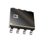
| 描述 | IC OPAMP CHOPPER 1.5MHZ 8SOIC精密放大器 Zero-Drft SGL-Supply RRIO SGL |
| 产品分类 | Linear - Amplifiers - Instrumentation, OP Amps, Buffer Amps集成电路 - IC |
| 品牌 | Analog Devices |
| 产品手册 | |
| 产品图片 |
|
| rohs | 符合RoHS无铅 / 符合限制有害物质指令(RoHS)规范要求 |
| 产品系列 | 放大器 IC,精密放大器,Analog Devices AD8551ARZ-REEL7- |
| 数据手册 | |
| 产品型号 | AD8551ARZ-REEL7 |
| 产品培训模块 | http://www.digikey.cn/PTM/IndividualPTM.page?site=cn&lang=zhs&ptm=30008http://www.digikey.cn/PTM/IndividualPTM.page?site=cn&lang=zhs&ptm=26202 |
| 产品种类 | 精密放大器 |
| 供应商器件封装 | 8-SOIC |
| 共模抑制比—最小值 | 115 dB |
| 其它名称 | AD8551ARZ-REEL7-ND |
| 包装 | 带卷 (TR) |
| 压摆率 | 0.4 V/µs |
| 可用增益调整 | 125 dB |
| 商标 | Analog Devices |
| 增益带宽生成 | 1.5 MHz |
| 增益带宽积 | 1.5MHz |
| 安装类型 | 表面贴装 |
| 安装风格 | SMD/SMT |
| 封装 | Reel |
| 封装/外壳 | 8-SOIC(0.154",3.90mm 宽) |
| 封装/箱体 | SOIC-8 |
| 工作温度 | -40°C ~ 125°C |
| 工作电源电压 | 2.7 V to 6 V |
| 工厂包装数量 | 1000 |
| 放大器类型 | 断路器(零漂移) |
| 最大工作温度 | + 125 C |
| 最小工作温度 | - 40 C |
| 标准包装 | 1,000 |
| 电压-电源,单/双 (±) | 2.7 V ~ 5.5 V |
| 电压-输入失调 | 1mV |
| 电压增益dB | 145 dB |
| 电流-电源 | 850µA |
| 电流-输入偏置 | 10pA |
| 电流-输出/通道 | 30mA |
| 电源电压-最大 | 6 V |
| 电源电压-最小 | 2.7 V |
| 电源电流 | 975 uA |
| 电源类型 | Single |
| 电路数 | 1 |
| 系列 | AD8551 |
| 视频文件 | http://www.digikey.cn/classic/video.aspx?PlayerID=1364138032001&width=640&height=505&videoID=2245193153001http://www.digikey.cn/classic/video.aspx?PlayerID=1364138032001&width=640&height=505&videoID=2245193159001 |
| 输入偏压电流—最大 | 1.5 nA |
| 输入补偿电压 | 1 uV |
| 输出类型 | 满摆幅 |
| 通道数量 | 1 Channel |


- 商务部:美国ITC正式对集成电路等产品启动337调查
- 曝三星4nm工艺存在良率问题 高通将骁龙8 Gen1或转产台积电
- 太阳诱电将投资9.5亿元在常州建新厂生产MLCC 预计2023年完工
- 英特尔发布欧洲新工厂建设计划 深化IDM 2.0 战略
- 台积电先进制程称霸业界 有大客户加持明年业绩稳了
- 达到5530亿美元!SIA预计今年全球半导体销售额将创下新高
- 英特尔拟将自动驾驶子公司Mobileye上市 估值或超500亿美元
- 三星加码芯片和SET,合并消费电子和移动部门,撤换高东真等 CEO
- 三星电子宣布重大人事变动 还合并消费电子和移动部门
- 海关总署:前11个月进口集成电路产品价值2.52万亿元 增长14.8%


PDF Datasheet 数据手册内容提取
Zero-Drift, Single-Supply, Rail-to-Rail Input/Output Operational Amplifiers Data Sheet AD8551/AD8552/AD8554 FEATURES PIN CONFIGURATIONS Low offset voltage: 1 μV Input offset drift: 0.005 μV/°C NC 1 8 NC –IN A AD8551 V+ Rail-to-rail input and output swing +IN A OUT A 5H iVg/h2 .g7a Vin s,i CngMlRe-Rs,u PpSpRlRy :o 1p3e0r adtBio n FigVu–reN 1C. 8=4 -NLOea CdO MN5NSEOCPT (RNMC Suffix01101-001) Ultralow input bias current: 20 pA Low supply current: 700 μA/op amp NC 1 8 NC Overload recovery time: 50 μs –IN A 2 7 V+ AD8551 No external capacitors required +IN A 3 6 OUT A V– 4 5 NC ATePmPpLeIrCatAuTreIO seNnSso rs NC = NO CONNECT 01101-002 Figure 2. 8-Lead SOIC (R Suffix) Pressure sensors Precision current sensing OUT A 1 8 V+ SMteradiinc agla ignest arummpelinfiteartsi o n +–IINNV AA– 4AD85525 O–+IIUNNT BB B 01101-003 Thermocouple amplifiers Figure 3. 8-Lead TSSOP (RU Suffix) GENERAL DESCRIPTION OUT A 1 8 V+ This family of amplifiers has ultralow offset, drift, and bias –IN A 2 7 OUT B current. The AD8551, AD8552, and AD8554 are single, dual, +IN A 3 AD8552 6 –IN B aAnlld a qreu gauda armanpteliefdie tros ofepaetruartien fgro rmail 2-t.o7- Vra itlo i n5p Vu tw ainthd ao usitnpgulte sswuipnpglsy.. V– 4 5 +IN B 01101-004 Figure 4. 8-Lead SOIC (R Suffix) The AD8551/AD8552/AD8554 provide the benefits previously found only in expensive auto-zeroing or chopper-stabilized OUT A 1 14 OUT D –IN A –IN D amplifiers. Using Analog Devices, Inc. topology, these new +IN A +IN D V+ AD8554 V– zeexrtoer-ndaril fct aapmacpiltiofiresr sa rceo rmeqbuiniree ldo.w cost with high accuracy. No O+–UIINNT BBB 7 8 –O+IIUNNT CC C 01101-005 Figure 5. 14-Lead TSSOP (RU Suffix) With an offset voltage of only 1 μV and drift of 0.005 μV/°C, the AD8551/AD8552/AD8554 are perfectly suited for applications in which error sources cannot be tolerated. Temperature, OUT A 1 14 OUT D position and pressure sensors, medical equipment, and strain –IN A 2 13 –IN D gage amplifiers benefit greatly from nearly zero drift over their +IN A 3 12 +IN D operating temperature range. The rail-to-rail input and output V+ 4 AD8554 11 V– swings provided by the AD8551/AD8552/AD8554 make both +IN B 5 10 +IN C hTihgeh A-sDid8e5 a5n1d/A loDw8-5si5d2e/ AseDn8si5n5g4 e aarsey .s p ecified for the extended O–UINT BB 67 98 –OIUNT C C 01101-006 Figure 6. 14-Lead SOIC (R Suffix) industrial/automotive temperature range (−40°C to +125°C). The AD8551 single amplifier is available in 8-lead MSOP and 8-lead narrow SOIC packages. The AD8552 dual amplifier is available in 8-lead narrow SOIC and 8-lead TSSOP surface- mount packages. The AD8554 quad is available in 14-lead narrow SOIC and 14-lead TSSOP packages. Rev. F Document Feedback Information furnished by Analog Devices is believed to be accurate and reliable. However, no responsibility is assumed by Analog Devices for its use, nor for any infringements of patents or other One Technology Way, P.O. Box 9106, Norwood, MA 02062-9106, U.S.A. rights of third parties that may result from its use. Specifications subject to change without notice. No license is granted by implication or otherwise under any patent or patent rights of Analog Devices. Tel: 781.329.4700 ©1999–2015 Analog Devices, Inc. All rights reserved. Trademarks and registered trademarks are the property of their respective owners. Technical Support www.analog.com
AD8551/AD8552/AD8554 Data Sheet TABLE OF CONTENTS Features .............................................................................................. 1 1/f Noise Characteristics ........................................................... 16 Applications ....................................................................................... 1 Intermodulation Distortion ...................................................... 17 General Description ......................................................................... 1 Broadband and External Resistor Noise Considerations ...... 18 Pin Configurations ........................................................................... 1 Output Overdrive Recovery ...................................................... 18 Revision History ............................................................................... 2 Input Overvoltage Protection ................................................... 18 Specifications ..................................................................................... 3 Output Phase Reversal ............................................................... 18 Electrical Characteristics ............................................................. 3 Capacitive Load Drive ............................................................... 19 Absolute Maximum Ratings ............................................................ 5 Power-Up Behavior .................................................................... 19 Thermal Characteristics .............................................................. 5 Applications Information .............................................................. 20 ESD Caution .................................................................................. 5 A 5 V Precision Strain Gage Circuit ........................................ 20 Typical Performance Characteristics ............................................. 6 3 V Instrumentation Amplifier ................................................ 20 Functional Description .................................................................. 14 A High Accuracy Thermocouple Amplifier ........................... 21 Amplifier Architecture .............................................................. 14 Precision Current Meter ............................................................ 21 Basic Auto-Zero Amplifier Theory .......................................... 14 Precision Voltage Comparator .................................................. 21 High Gain, CMRR, PSRR .......................................................... 15 Outline Dimensions ....................................................................... 22 Maximizing Performance Through Proper Layout ............... 16 Ordering Guide .......................................................................... 24 REVISION HISTORY 6/15—Rev. E to Rev. F 3/07—Rev. B to Rev. C Change to Input Voltage Parameter, Table 3 ................................. 5 Changes to Specifications Section ................................................... 3 11/12—Rev.D to Rev. E 2/07—Rev. A to Rev. B Changes to Figure 68 ...................................................................... 21 Updated Format .................................................................. Universal Updated Outline Dimensions (RM-8) ......................................... 22 Changes to Figure 54 ...................................................................... 16 Changes to Ordering Guide .......................................................... 24 Deleted Spice Model Section ........................................................ 19 Deleted Figure 63, Renumbered Sequentially ............................ 19 9/08—Rev. C to Rev. D Changes to Ordering Guide .......................................................... 24 Changes to Ordering Guide .......................................................... 23 11/02—Rev. 0 to Rev. A Edits to Figure 60 ............................................................................ 16 Updated Outline Dimensions ....................................................... 20 Rev. F | Page 2 of 24
Data Sheet AD8551/AD8552/AD8554 SPECIFICATIONS ELECTRICAL CHARACTERISTICS V = 5 V, V = 2.5 V, V = 2.5 V, T = 25°C, unless otherwise noted. S CM O A Table 1. Parameter Symbol Conditions Min Typ Max Unit INPUT CHARACTERISTICS Offset Voltage V 1 5 μV OS −40°C ≤ T ≤ +125°C 10 μV A Input Bias Current I 10 50 pA B AD8551/AD8554 −40°C ≤ T ≤ +125°C 1.0 1.5 nA A AD8552 −40°C ≤ T ≤ +85°C 160 300 pA A AD8552 −40°C ≤ T ≤ +125°C 2.5 4 nA A Input Offset Current I 20 70 pA OS AD8551/AD8554 −40°C ≤ T ≤ +125°C 150 200 pA A AD8552 −40°C ≤ T ≤ +85°C 30 150 pA A AD8552 −40°C ≤ T ≤ +125°C 150 400 pA A Input Voltage Range 0 5 V Common-Mode Rejection Ratio CMRR V = 0 V to +5 V 120 140 dB CM −40°C ≤ T ≤ +125°C 115 130 dB A Large Signal Voltage Gain1 A R = 10 kΩ, V = 0.3 V to 4.7 V 125 145 dB VO L O −40°C ≤ T ≤ +125°C 120 135 dB A Offset Voltage Drift ΔV /ΔT −40°C ≤ T ≤ +125°C 0.005 0.04 μV/°C OS A OUTPUT CHARACTERISTICS Output Voltage High V R = 100 kΩ to GND 4.99 4.998 V OH L R = 100 kΩ to GND @ −40°C to +125°C 4.99 4.997 V L R = 10 kΩ to GND 4.95 4.98 V L R = 10 kΩ to GND @ −40°C to +125°C 4.95 4.975 V L Output Voltage Low V R = 100 kΩ to V+ 1 10 mV OL L R = 100 kΩ to V+ @ −40°C to +125°C 2 10 mV L R = 10 kΩ to V+ 10 30 mV L R = 10 kΩ to V+ @ −40°C to +125°C 15 30 mV L Output Short-Circuit Limit Current I ±25 ±50 mA SC −40°C to +125°C ±40 mA Output Current I ±30 mA O −40°C to +125°C ±15 mA POWER SUPPLY Power Supply Rejection Ratio PSRR V = 2.7 V to 5.5 V 120 130 dB S −40°C ≤ T ≤ +125°C 115 130 dB A Supply Current/Amplifier I V = 0 V 850 975 μA SY O −40°C ≤ T ≤ +125°C 1000 1075 μA A DYNAMIC PERFORMANCE Slew Rate SR R = 10 kΩ 0.4 V/μs L Overload Recovery Time 0.05 0.3 ms Gain Bandwidth Product GBP 1.5 MHz NOISE PERFORMANCE Voltage Noise e p-p 0 Hz to 10 Hz 1.0 μV p-p n e p-p 0 Hz to 1 Hz 0.32 μV p-p n Voltage Noise Density e f = 1 kHz 42 nV/√Hz n Current Noise Density i f = 10 Hz 2 fA/√Hz n 1 Gain testing is dependent upon test bandwidth. Rev. F | Page 3 of 24
AD8551/AD8552/AD8554 Data Sheet V = 2.7 V, V = 1.35 V, V = 1.35 V, T = 25°C, unless otherwise noted. S CM O A Table 2. Parameter Symbol Conditions Min Typ Max Unit INPUT CHARACTERISTICS Offset Voltage V 1 5 μV OS −40°C ≤ T ≤ +125°C 10 μV A Input Bias Current I 10 50 pA B AD8551/AD8554 −40°C ≤ T ≤ +125°C 1.0 1.5 nA A AD8552 −40°C ≤ T ≤ +85°C 160 300 pA A AD8552 −40°C ≤ T ≤ +125°C 2.5 4 nA A Input Offset Current I 10 50 pA OS AD8551/AD8554 −40°C ≤ T ≤ +125°C 150 200 pA A AD8552 −40°C ≤ T ≤ +85°C 30 150 pA A AD8552 −40°C ≤ T ≤ +125°C 150 400 pA A Input Voltage Range 0 2.7 V Common-Mode Rejection Ratio CMRR V = 0 V to 2.7 V 115 130 dB CM −40°C ≤ T ≤ +125°C 110 130 dB A Large Signal Voltage Gain1 A R = 10 kΩ, V = 0.3 V to 2.4 V 110 140 dB VO L O −40°C ≤ T ≤ +125°C 105 130 dB A Offset Voltage Drift ΔV /ΔT −40°C ≤ T ≤ +125°C 0.005 0.04 μV/°C OS A OUTPUT CHARACTERISTICS Output Voltage High V R = 100 kΩ to GND 2.685 2.697 V OH L R = 100 kΩ to GND @ −40°C to +125°C 2.685 2.696 V L R = 10 kΩ to GND 2.67 2.68 V L R = 10 kΩ to GND @ −40°C to +125°C 2.67 2.675 V L Output Voltage Low V R = 100 kΩ to V+ 1 10 mV OL L R = 100 kΩ to V+ @ −40°C to +125°C 2 10 mV L R = 10 kΩ to V+ 10 20 mV L R = 10 kΩ to V+ @ −40°C to +125°C 15 20 mV L Short-Circuit Limit I ±10 ±15 mA SC −40°C to +125°C ±10 mA Output Current I ±10 mA O −40°C to +125°C ±5 mA POWER SUPPLY Power Supply Rejection Ratio PSRR V = 2.7 V to 5.5 V 120 130 dB S −40°C ≤ T ≤ +125°C 115 130 dB A Supply Current/Amplifier I V = 0 V 750 900 μA SY O −40°C ≤ T ≤ +125°C 950 1000 μA A DYNAMIC PERFORMANCE Slew Rate SR R = 10 kΩ 0.5 V/μs L Overload Recovery Time 0.05 ms Gain Bandwidth Product GBP 1 MHz NOISE PERFORMANCE Voltage Noise e p-p 0 Hz to 10 Hz 1.6 μV p-p n Voltage Noise Density e f = 1 kHz 75 nV/√Hz n Current Noise Density i f = 10 Hz 2 fA/√Hz n 1 Gain testing is dependent upon test bandwidth. Rev. F | Page 4 of 24
Data Sheet AD8551/AD8552/AD8554 ABSOLUTE MAXIMUM RATINGS Table 3. THERMAL CHARACTERISTICS Parameter Rating Table 4. Supply Voltage 6 V Package Type θ θ Unit Input Voltage GND −0.3 V to V + 0.3 V JA JC S 8-Lead MSOP (RM) 190 44 °C/W Differential Input Voltage1 ±5.0 V 8-Lead TSSOP (RU) 240 43 °C/W ESD (Human Body Model) 2000 V 8-Lead SOIC (R) 158 43 °C/W Output Short-Circuit Duration to GND Indefinite 14-Lead TSSOP (RU) 180 36 °C/W Storage Temperature Range −65°C to +150°C 14-Lead SOIC (R) 120 36 °C/W Operating Temperature Range −40°C to +125°C Junction Temperature Range −65°C to +150°C ESD CAUTION Lead Temperature Range 300°C (Soldering, 60 sec) 1 Differential input voltage is limited to ±5.0 V or the supply voltage, whichever is less. Stresses at or above those listed under Absolute Maximum Ratings may cause permanent damage to the product. This is a stress rating only; functional operation of the product at these or any other conditions above those indicated in the operational section of this specification is not implied. Operation beyond the maximum operating conditions for extended periods may affect product reliability. Rev. F | Page 5 of 24
AD8551/AD8552/AD8554 Data Sheet TYPICAL PERFORMANCE CHARACTERISTICS 180 180 VSY = 2.7V VSY = 5V 160 VCM = 1.35V 160 VCM = 2.5V TA = 25°C TA = 25°C 140 140 S S R R E E FI120 FI120 LI LI P P M100 M100 A A F F R O 80 R O 80 E E MB 60 MB 60 U U N N 40 40 20 20 0–2.5 –1.5 O–F0F.5SET VOL0T.A5GE (µV)1.5 2.5 01101-007 0–2.5 –1.5 O–F0F.5SET VOL0T.A5GE (µV)1.5 2.5 01101-010 Figure 7. Input Offset Voltage Distribution at 2.7 V Figure 10. Input Offset Voltage Distribution at 5 V 50 12 40 VTASY = = – 450V°C, +25°C, +85°C VVSCYM == 52V.5V +85°C 10 TA = –40°C TO +125°C A) 30 S p R ENT ( 20 LIFIE 8 R P R M U A S C 10 OF 6 UT BIA 0 +25°C MBER 4 P –40°C U IN–10 N 2 –20 –300 1INPUT COMM2ON-MODE V3OLTAGE (V4) 5 01101-008 00 1 INPU2T OFFSE3T DRIFT (n4V/°C) 5 6 01101-011 Figure 8. Input Bias Current vs. Common-Mode Voltage Figure 11. Input Offset Voltage Drift Distribution at 5 V 1500 10k 1000 TVASY = = 1 255V°C TVASY = = 2 55°VC 1k A) T (p 500 mV) RREN 0 AGE (100 U T C L BIAS –500 UT VO 10 SOURCE T P U T NP–1000 OU SINK I 1 –1500 –20000 1INPUT COMM2ON-MODE V3OLTAGE (V4) 5 01101-009 00..10001 0.001 0.0L1OAD CU0R.R1ENT (mA1) 10 100 01101-012 Figure 9. Input Bias Current vs. Common-Mode Voltage Figure 12. Output Voltage to Supply Rail vs. Load Current at 5 V Rev. F | Page 6 of 24
Data Sheet AD8551/AD8552/AD8554 10k 800 VSY = 2.7V TA = +25°C TA = 25°C µA)700 1k R ( E mV) PLIFI600 AGE (100 R AM500 OLT T PE400 UTPUT V 10 SOURCESINK CURREN300 O Y 200 L 1 P P SU100 00..10001 0.001 0.0L1OAD CU0R.R1ENT (mA1) 10 100 01101-013 00 1 S2UPPLY VO3LTAGE (V4) 5 6 01101-016 Figure 13. Output Voltage to Supply Rail vs. Load Current at 2.7 V Figure 16. Supply Current per Amplifier vs. Supply Voltage 0 60 VSY = 2.7V VVCSYM == 52V.5V 5400 RCLL == ∞0pF 0 NT (pA) –250 N (dB) 30 45 grees) PUT BIAS CURRE –500 OPEN-LOOP GAI–1210000 91120382505 PHASE SHIFT (De IN –750 –20 270 –30 –1000–75 –50 –25 0TEMP2E5RATU5R0E (°C7)5 100 125 150 01101-014 –4010k 100k FREQUE1NMCY (Hz) 10M 100M 01101-017 Figure 14. Input Bias Current vs. Temperature Figure 17. Open-Loop Gain and Phase Shift vs. Frequency at 2.7 V 1.0 60 VVCSYM == 52V.5V 5V 50 VCRSLLY == = ∞0 p5VF 0.8 40 0 NT (mA)0.6 2.7V AIN (dB) 3200 4950 Degrees) SUPPLY CURRE0.4 OPEN-LOOP G–11000 112382550 PHASE SHIFT ( 0.2 –20 270 –30 0–75 –50 –25 0TEMP2E5RATU5R0E (°C7)5 100 125 150 01101-015 –4010k 100k FREQUE1NMCY (Hz) 10M 100M 01101-018 Figure 15. Supply Current vs. Temperature Figure 18. Open-Loop Gain and Phase Shift vs. Frequency at 5 V Rev. F | Page 7 of 24
AD8551/AD8552/AD8554 Data Sheet 60 300 5400 AV = –100 VCRSLLY == = 20 kp2Ω.F7V 227400 VSY = 5V GAIN (dB) 3200 AV = –10 ANCE (Ω)211800 ED-LOOP 100 AV = +1 UT IMPED115200 CLOS–10 OUTP 90 AV = 100 –20 60 AV = 10 AV = 1 –30 30 –40100 1k F1R0EkQUENCY1 (0H0zk) 1M 10M 01101-019 0100 1k F1R0EkQUENCY1 (0H0zk) 1M 10M 01101-022 Figure 19. Closed-Loop Gain vs. Frequency at 2.7 V Figure 22. Output Impedance vs. Frequency at 5 V 60 B) 5400 AV = –100 VRCSLLY == = 20 kp5ΩVF VCRASLLVY === = 231 k02Ω0.7pVF AIN (d 3200 AV = –10 G P OO 10 D-L 0 AV = +1 E S LO–10 C –20 ––4300100 1k F1R0EkQUENCY1 (0H0zk) 1M 10M 01101-020 2µs 500mV 01101-023 Figure 20. Closed-Loop Gain vs. Frequency at 5 V Figure 23. Large Signal Transient Response at 2.7 V 300 270 VSY = 2.7V VSY = 5V CL = 300pF 240 RL = 2kΩ Ω) AV = 1 E (210 C AN180 D E P150 M UT I120 P T OU 90 AV = 100 60 AV = 10 300100 1k F1R0EkQUENCY1 (0H0zk) AV 1=M 1 10M 01101-021 5µs 1V 01101-024 Figure 21. Output Impedance vs. Frequency at 2.7 V Figure 24. Large Signal Transient Response at 5 V Rev. F | Page 8 of 24
Data Sheet AD8551/AD8552/AD8554 45 VSY = ±1.35V VSY = ±2.5V CL = 50pF 40 RL = 2kΩ RL =∞ %) TA = 25°C AV = 1 T (35 O O H30 S R VE25 O L A20 N G L SI15 +OS –OS L A M10 S 5µs 50mV 01101-025 0510 100CAPACITANCE (pF1)k 10k 01101-028 Figure 25. Small Signal Transient Response at 2.7 V Figure 28. Small Signal Overshoot vs. Load Capacitance at 5 V VSY = ±2.5V CL = 50pF 0V RL =∞ AV = 1 VIN VSY = ±2.5V VIN = –200mV p-p (RET TO GND) CL = 0pF RL = 10kΩ VOUT AV = –100 5µs 50mV 01101-026 0VBTOOPT TSOCMA LSE2C0:A µ2Ls0E0m: 1VV/D/DIVIV 1V 01101-029 Figure 26. Small Signal Transient Response at 5 V Figure 29. Positive Overvoltage Recovery 50 VSY = ±1.35V %)4450 RTAL == 225k°ΩC VIN OOT (35 0V SH VSY = ±2.5V ER30 VIN = 200mV p-p AL OV25 +OS 0V C L(R =E 0Tp TFO GND) L SIGN2105 –OS RALV == 1–01k0Ω0 L A SM10 VOUT 5 20µs 1V 010 100CAPACITANCE (pF1)k 10k 01101-027 BTOOPT TSOCMA LSEC:A 2L0E0m: 1VV/D/DIVIV 01101-030 Figure 27. Small Signal Overshoot vs. Load Capacitance at 2.7 V Figure 30. Negative Overvoltage Recovery Rev. F | Page 9 of 24
AD8551/AD8552/AD8554 Data Sheet 140 VS = ±2.5V VSY = ±1.35V RL = 2kΩ AV = –100 120 VIN = 60mV p-p 100 B) 80 d R ( R S 60 P +PSRR 40 –PSRR 200µs 1V 01101-031 200100 1k F1R0EkQUENCY1 (0H0zk) 1M 10M 01101-034 Figure 31. No Phase Reversal Figure 34. PSRR vs. Frequency at ±1.35 V 140 140 VSY = 2.7V VSY = ±2.5V 120 120 100 100 B) 80 B) 80 d d RR ( RR ( +PSRR M 60 S 60 C P 40 40 –PSRR 20 20 0100 1k F1R0EkQUENCY1 (0H0zk) 1M 10M 01101-032 0100 1k F1R0EkQUENCY1 (0H0zk) 1M 10M 01101-035 Figure 32. CMRR vs. Frequency at 2.7 V Figure 35. PSRR vs. Frequency at ±2.5 V 140 3.0 VSY = 5V VSY = ±1.35V RL = 2kΩ 120 2.5 AV = 1 THD+N < 1% 100 p) TA = 25°C V p-2.0 dB) 80 NG ( R ( WI1.5 MR 60 T S C U P UT1.0 40 O 0.5 20 0100 1k F1R0EkQUENCY1 (0H0zk) 1M 10M 01101-033 0100 1k FREQU1E0NkCY (Hz) 100k 1M 01101-036 Figure 33. CMRR vs. Frequency at 5 V Figure 36. Maximum Output Swing vs. Frequency at 2.7 V Rev. F | Page 10 of 24
Data Sheet AD8551/AD8552/AD8554 5.5 45..50 ARVSLVY == = 21 k±Ω2.5V 182 VRSSY = = 0 2Ω.7V THD+N < 1% p)4.0 TA = 25°C 156 p- V 3.5 NG (3.0 Hz)130 UT SWI2.5 (nV/√n104 TP2.0 e 78 U O1.5 52 1.0 0.5 26 0100 1k FREQU1E0NkCY (Hz) 100k 1M 01101-037 0 0.5 FR1E.0QUENCY (1k.H5z) 2.0 2.5 01101-040 Figure 37. Maximum Output Swing vs. Frequency at 5 V Figure 40. Voltage Noise Density at 2.7 V from 0 Hz to 2.5 kHz VSY = ±1.35V VSY = 2.7V AV = 10000 112 RS = 0Ω 96 80 Hz) √ 0V V/ 64 n (n e 48 32 1s 2mV 01101-038 160 5 FR1E0QUENCY (k1H5z) 20 25 01101-041 Figure 38. 0.1 Hz to 10 Hz Noise at 2.7 V Figure 41. Voltage Noise Density at 2.7 V from 0 Hz to 25 kHz VSY = ±2.5V VSY = 5V AV = 10000 91 RS = 0Ω 78 65 Hz) √ V/52 n (n e 39 26 1s 2mV 01101-039 130 0.5 FR1E.0QUENCY (1k.H5z) 2.0 2.5 01101-042 Figure 39. 0.1 Hz to 10 Hz Noise at 5 V Figure 42. Voltage Noise Density at 5 V from 0 Hz to 2.5 kHz Rev. F | Page 11 of 24
AD8551/AD8552/AD8554 Data Sheet 150 VSY = 5V VSY = 2.7V TO 5.5V 112 RS = 0Ω dB)145 96 N ( O TI Hz) 80 EJEC140 √ R V/ 64 Y e (nn 48 SUPPL135 R E 32 W O130 P 16 0 5 FR1E0QUENCY (k1H5z) 20 25 01101-043 125–75 –50 –25 0TEMP2E5RATU5R0E (°C7)5 100 125 150 01101-045 Figure 43. Voltage Noise Density at 5 V from 0 Hz to 25 kHz Figure 45. Power Supply Rejection vs. Temperature 50 VSY = 5V VSY = 2.7V 168 RS = 0Ω 40 A) 30 144 NT (m 20 ISC– e (nV/√Hz)n1279026 CIRCUIT CURRE–11000 ISC+ RT-–20 48 O H S–30 24 –40 0 FREQUE5NCY (Hz) 10 01101-044 –50–75 –50 –25 0TEMP2E5RATU5R0E (°C7)5 100 125 150 01101-046 Figure 44. Voltage Noise Density at 5 V from 0 Hz to 10 Hz Figure 46. Output Short-Circuit Current vs. Temperature Rev. F | Page 12 of 24
Data Sheet AD8551/AD8552/AD8554 100 250 80 VSY = 5.0V V)225 VSY = 5.0V m mA) 60 ISC– AIL (200 NT ( 40 LY R175 E P URR 20 SUP150 RL = 1kΩ T C 0 TO 125 UI E C G R –20 A100 RT-CI –40 ISC+ VOLT 75 SHO –60 PUT 50 UT RL = 100kΩ –80 O 25 RL = 10kΩ –100–75 –50 –25 0TEMP2E5RATU5R0E (°C7)5 100 125 150 01101-047 0–75 –50 –25 0TEMP2E5RATU5R0E (°C7)5 100 125 150 01101-049 Figure 49. Output Voltage to Supply Rail vs. Temperature Figure 47. Output Short-Circuit Current vs. Temperature 250 V)225 VSY = 2.7V m AIL (200 R LY 175 P P U150 S O T125 GE RL = 1kΩ A100 T L VO 75 T PU 50 UT RL = 100kΩ O 25 RL = 10kΩ 0–75 –50 –25 0TEMP2E5RATU5R0E (°C7)5 100 125 150 01101-048 Figure 48. Output Voltage to Supply Rail vs. Temperature Rev. F | Page 13 of 24
AD8551/AD8552/AD8554 Data Sheet FUNCTIONAL DESCRIPTION some improvements made over time. The AD8551/AD8552/ The AD8551/AD8552/AD8554 are high precision, rail-to-rail AD8554 design offers a number of significant performance operational amplifiers that can be run from a single-supply voltage. improvements over previous versions while attaining a very Their typical offset voltage of less than 1 μV allows these amplifiers substantial reduction in device cost. This section offers a simplified to be easily configured for high gains without risk of excessive explanation of how the AD8551/AD8552/AD8554 are able to output voltage errors. The extremely small temperature drift of offer extremely low offset voltages and high open-loop gains. 5 nV/°C ensures a minimum of offset voltage error over its entire temperature range of −40°C to +125°C, making the As noted in the Amplifier Architecture section, each AD8551/ AD8551/AD8552/AD8554 amplifiers ideal for a variety of AD8552/AD8554 op amp contains two internal amplifiers. One sensitive measurement applications in harsh operating is used as the primary amplifier, the other as an autocorrection, environments, such as underhood and braking/suspension or nulling, amplifier. Each amplifier has an associated input systems in automobiles. offset voltage that can be modeled as a dc voltage source in series with the noninverting input. In Figure 50 and Figure 51 The AD8551/AD8552/AD8554 are CMOS amplifiers and these are labeled as V , where x denotes the amplifier achieve their high degree of precision through auto-zero OSX associated with the offset: A for the nulling amplifier and B for stabilization. This autocorrection topology allows the the primary amplifier. The open-loop gain for the +IN and −IN AD8551/AD8552/AD8554 to maintain its low offset voltage inputs of each amplifier is given as A . Both amplifiers also have over a wide temperature range and over its operating lifetime. X a third voltage input with an associated open-loop gain of B . X AMPLIFIER ARCHITECTURE There are two modes of operation determined by the action of Each AD8551/AD8552/AD8554 op amps consist of two two sets of switches in the amplifier: an auto-zero phase and an amplifiers, a main amplifier and a secondary amplifier, used amplification phase. to correct the offset voltage of the main amplifier. Both consist of a rail-to-rail input stage, allowing the input common-mode Auto-Zero Phase voltage range to reach both supply rails. The input stage consists In this phase, all φA switches are closed and all φB switches are of an NMOS differential pair operating concurrently with a opened. Here, the nulling amplifier is taken out of the gain loop parallel PMOS differential pair. The outputs from the by shorting its two inputs together. Of course, there is a degree differential input stages are combined in another gain stage of offset voltage, shown as V , inherent in the nulling amplifier OSA whose output is used to drive a rail-to-rail output stage. which maintains a potential difference between the +IN and −IN inputs. The nulling amplifier feedback loop is closed through The wide voltage swing of the amplifier is achieved by using two φB and V appears at the output of the nulling amp and on output transistors in a common-source configuration. The output 2 OSA C , an internal capacitor in the AD8551/AD8552/AD8554. voltage range is limited by the drain-to-source resistance of M1 Mathematically, this is expressed in the time domain as these transistors. As the amplifier is required to source or sink more output current, the rDS of these transistors increases, raising VOA[t] = AAVOSA[t] − BAVOA[t] (1) the voltage drop across these transistors. Simply put, the output which can be expressed as voltage does not swing as close to the rail under heavy output current conditions as it does with light output current. This is a A V t V t A OSA (2) characteristic of all rail-to-rail output amplifiers. Figure 12 and OA 1B A Figure 13 show how close the output voltage can get to the rails with a given output current. The output of the AD8551/AD8552/ This demonstrates that the offset voltage of the nulling amplifier AD8554 is short-circuit protected to approximately 50 mA of times a gain factor appears at the output of the nulling amplifier current. and, thus, on the CM1 capacitor. The AD8551/AD8552/AD8554 amplifiers have exceptional gain, VIN+ AB VOUT yielding greater than 120 dB of open-loop gain with a load of 2 kΩ. VIN– BB Because the output transistors are configured in a common-source ФB configuration, the gain of the output stage, and thus the open- VOSA VOA ФB CM2 ФA + loop gain of the amplifier, is dependent on the load resistance. AA VNB Open-loop gain decreases with smaller load resistances. This is another characteristic of rail-to-rail output amplifiers. –BA ФA CM1 BASIC AUTO-ZERO AMPLIFIER THEORY VNA 01101-050 Autocorrection amplifiers are not a new technology. Various IC Figure 50. Auto-Zero Phase of the AD8551/AD8552/AD8554 implementations have been available for more than 15 years with Rev. F | Page 14 of 24
Data Sheet AD8551/AD8552/AD8554 Amplification Phase the nulling amplifier has greatly reduced its own offset voltage error even before correcting the primary amplifier. This results When the φB switches close and the φA switches open for the in the primary amplifier output voltage becoming the voltage at amplification phase, this offset voltage remains on C and, M1 the output of the AD8551/AD8552/AD8554 amplifiers. It is essentially, corrects any error from the nulling amplifier. The equal to voltage across C is designated as V . Furthermore, V is M1 NA IN designated as the potential difference between the two inputs to V [t]=A (V [t]+V )+B V (8) OUT B IN OSB B NB the primary amplifier, or V = (V − V ). Thus, the nulling IN IN+ IN− amplifier can be expressed as In the amplification phase, VOA = VNB, so this can be rewritten as V [t]=A (V [t]−V [t])−B V [t] (3) OA A IN OSA A NA V VIN+ VOUT[t]=ABVIN[t]+ABVOSB +BBAAVIN[t]+1+OBSBA (9) AB VOUT VIN– BB Combining terms, ФB VOSA+ VOA ФB CM2 V [t]=V [t](A +A B )+ AABAVOSA +A V (10) ФA AA VNB OUT IN B B B 1+BA B OSA –BA ФA CM1 The AD8551/AD8552/AD8554 architecture is optimized in VNA 01101-051 such Aa Aw =a yA tBh aant d BA = BB and BA >> 1 Figure 51. Output Phase of the Amplifier Also, the gain product of A B is much greater than A . These A B B Because φA is now open and there is no place for CM1 to discharge, allow Equation 10 to be simplified to the voltage (VNA), at the present time (t), is equal to the voltage V [t]≈V [t]A B +A (V +V ) (11) at the output of the nulling amp (V ) at the time when φA was OUT IN A A A OSA OSB OA closed. If the period of the autocorrection switching frequency is Most obvious is the gain product of both the primary and nulling labeled t, then the amplifier switches between phases every 0.5 × t. S S amplifiers. This A B term is what gives the AD8551/AD8552/ A A Therefore, in the amplification phase AD8554 its extremely high open-loop gain. To understand how V [t]=V t−1t (4) VOSA and VOSB relate to the overall effective input offset voltage of NA NA 2 S the complete amplifier, establish the generic amplifier equation of ( ) V =k× V +V (12) Substituting Equation 4 and Equation 2 into Equation 3 yields OUT IN OS,EFF 1 where k is the open-loop gain of an amplifier and VOS, EFF is its A B V t− t V [t]=A V [t]+A V [t]− A A OSA 2 S (5) effective offset voltage. OA A IN A OSA 1+B A Putting Equation 12 into the form of Equation 11 gives For the sake of simplification, assume that the autocorrection V [t]≈V [t]A B +V A B (13) OUT IN A A OS,EFF A A frequency is much faster than any potential change in V or OSA V . This is a valid assumption because changes in offset voltage Thus, it is evident that OSB are a function of temperature variation or long-term wear time, V +V V ≈ OSA OSB (14) both of which are much slower than the auto-zero clock frequency OS,EFF B A of the AD8551/AD8552/AD8554. This effectively renders V OS The offset voltages of both the primary and nulling amplifiers time invariant; therefore, Equation 5 can be rearranged and are reduced by the Gain Factor B . This takes a typical input A rewritten as offset voltage from several millivolts down to an effective input V [t]=A V [t]+ AA(1+BA)VOSA−AABAVOSA (6) offset voltage of submicrovolts. This autocorrection scheme is OA A IN 1+B the outstanding feature of the AD8551/AD8552/AD8554 series A that continues to earn the reputation of being among the most or precise amplifiers available on the market. V HIGH GAIN, CMRR, PSRR VOA[t]=AAVIN[t]+1+OBSA (7) A Common-mode and power supply rejection are indications of the amount of offset voltage an amplifier has as a result of a change From these equations, the auto-zeroing action becomes evident. in its input common-mode or power supply voltages. As shown Note the V term is reduced by a 1 + B factor. This shows how OS A in the previous section, the autocorrection architecture of the Rev. F | Page 15 of 24
AD8551/AD8552/AD8554 Data Sheet AD8551/AD8552/AD8554 allows it to quite effectively PC board at one end of the component (T ) is different from A1 minimize offset voltages. The technique also corrects for offset the temperature at the other end (T ), the resulting Seebeck A2 errors caused by common-mode voltage swings and power voltages are not equal, resulting in a thermal voltage error. supply variations. This results in superb CMRR and PSRR This thermocouple error can be reduced by using dummy com- figures in excess of 130 dB. Because the autocorrection occurs ponents to match the thermoelectric error source. Placing the continuously, these figures can be maintained across the entire dummy component as close as possible to its partner ensures both temperature range of the device, from −40°C to +125°C. Seebeck voltages are equal, thus canceling the thermocouple error. MAXIMIZING PERFORMANCE THROUGH Maintaining a constant ambient temperature on the circuit board PROPER LAYOUT further reduces this error. The use of a ground plane helps distrib- ute heat throughout the board and reduces EMI noise pickup. To achieve the maximum performance of the extremely high input impedance and low offset voltage of the AD8551/ COMPONENT AD8552/AD8554, care is needed in laying out the circuit board. LEAD The PC board surface must remain clean and free of moisture to VSC1 + SURFACE-MOUNT +VSC2 SOLDER avoid leakage currents between adjacent traces. Surface coating COMPONENT VTS1 + + VTS2 of the circuit board reduces surface moisture and provides a humidity barrier, reducing parasitic resistance on the board. PC BOARD The use of guard rings around the amplifier inputs further reduces lceoankfaiggeu cruatriroenn,t sa.n Fdig Fuirgeu 5re2 5s3h oswhosw psr othpee rt ogpu avride wri nogf a surface- CTORPAPCEER TA1 VIFT ST1A 1+ ≠V TSTCAA122 ,≠ T VHTESN2 + VSC2 01101-054 mount layout. The guard ring does not need to be a specific Figure 54. Mismatch in Seebeck Voltages Causes width, but it should form a continuous loop around both inputs. Thermoelectric Voltage Error By setting the guard ring voltage equal to the voltage at the RF noninverting input, parasitic capacitance is minimized as well. For further reduction of leakage currents, components can be R1 mounted to the PC board using Teflon standoff insulators. VOUT VIN AD8551/ RS = R1 AD8552/ AD8554 AV = 1 + (RF/R1) VOUT VOUT NOTES VIN AD8552 VIN AD8552 1 . RASL ISGHNOMUELNDT BTEO PRL1A TCOE BDA INL ACNLCOES ES EPERBOEXCIMK IVTOY LATNADGES. 01101-055 Figure 55. Using Dummy Components to Cancel Thermoelectric Voltage Errors VIN VOUT 1/f NOISE CHARACTERISTICS AD8552 01101-052 Another advantage of auto-zero amplifiers is their ability to Figure 52. Guard Ring Layout and Connections to Reduce cancel flicker noise. Flicker noise, also known as 1/f noise, is PC Board Leakage Currents noise inherent in the physics of semiconductor devices, and it increases 3 dB for every octave decrease in frequency. The 1/f V+ R1 R2 AD8552 corner frequency of an amplifier is the frequency at which the VIN1 R2 R1 flicker noise is equal to the broadband noise of the amplifier. VIN2 At lower frequencies, flicker noise dominates, causing higher degrees of error for sub-Hertz frequencies or dc precision GUARD RING VREF GUARD applications. V– VREF RING 01101-053 Because the AD8551/AD8552/AD8554 amplifiers are self- Figure 53. Top View of AD8552 SOIC Layout with Guard Rings correcting op amps, they do not have increasing flicker noise at lower frequencies. In essence, low frequency noise is treated as a Other potential sources of offset error are thermoelectric slowly varying offset error and is greatly reduced as a result of voltages on the circuit board. This voltage, also called Seebeck autocorrection. The correction becomes more effective as the voltage, occurs at the junction of two dissimilar metals and is noise frequency approaches dc, offsetting the tendency of the proportional to the temperature of the junction. The most common noise to increase exponentially as frequency decreases. This metallic junctions on a circuit board are solder-to-board trace allows the AD8551/AD8552/AD8554 to have lower noise near and solder-to-component lead. Figure 54 shows a cross-section dc than standard low noise amplifiers that are susceptible to 1/f of the thermal voltage error sources. If the temperature of the noise. Rev. F | Page 16 of 24
Data Sheet AD8551/AD8552/AD8554 INTERMODULATION DISTORTION the amplifier. Figure 58 shows the spectral output of an AD8552 configured as a high gain stage (+60 dB) with a 1 mV input signal The AD8551/AD8552/AD8554 can be used as a conventional applied. The relative levels of all IMD products and harmonic op amp for gain/ bandwidth combinations up to 1.5 MHz. The distortion add up to produce an output error of −60 dB relative auto-zero correction frequency of the device is fixed at 4 kHz. to the input signal. At unity gain, these add up to only −120 dB Although a trace amount of this frequency feeds through to the relative to the input signal. output, the amplifier can be used at much higher frequencies. Figure 56 shows the spectral output of the AD8552 with the 0 amplifier configured for unity gain and the input grounded. OUTPUT SIGNAL VSY = 5V 1V rms @ 200Hz AV = 60dB –20 The 4 kHz auto-zero clock frequency appears at the output with less than 2 μV of amplitude. Harmonics are also present, but at dB) –40 reduced levels from the fundamental auto-zero clock frequency. AL ( N G The amplitude of the clock frequency feedthrough is proportional SI –60 T to the closed-loop gain of the amplifier. Like other autocorrection U P T amplifiers, at higher gains there is more clock frequency OU –80 IMD < 100µV rms feedthrough. Figure 57 shows the spectral output with the amplifier configured for a gain of 60 dB. –100 –200 VASVY = = 0 5dVB –1200 1 2 3 FR4EQUEN5CY (k6Hz) 7 8 9 10 01101-058 Figure 58. Spectral Analysis of AD8552 in High Gain with a 1 mV Input Signal B) –40 L (d For most low frequency applications, the small amount of auto- NA –60 zero clock frequency feedthrough does not affect the precision G UT SI –80 of the measurement system. If it is desired, the clock frequency P feedthrough can be reduced through the use of a feedback T U O–100 capacitor around the amplifier. However, this reduces the bandwidth of the amplifier. Figure 59 and Figure 60 show a –120 configuration for reducing the clock feedthrough and the corresponding spectral analysis at the output. The −3 dB –1400 1 2 3 FR4EQUEN5CY (k6Hz) 7 8 9 10 01101-056 bandwidth of this configuration is 480 Hz. Figure 56. Spectral Analysis of AD8552 Output in Unity Gain Configuration 3.3nF 0 100kΩ VSY = 5V AV = 60dB 100Ω –20 VIN = 1mV rms NAL (dB) ––4600 @ 200Hz 01101-059 G Figure 59. Reducing Autocorrection Clock Noise Using a Feedback Capacitor SI PUT –80 0 UT VSY = 5V O–100 AV = 60dB –20 –120 L –40 A –1400 1 2 3 FR4EQUEN5CY (k6Hz) 7 8 9 10 01101-057 T SIGN –60 U Figure 57. Spectral Analysis of AD8551/AD8552/AD8554 Output P T with +60 dB Gain OU –80 When an input signal is applied, the output contains some –100 degree of intermodulation distortion (IMD). This is another characteristic feature of all autocorrection amplifiers. IMD asipgpneaalr asn ads tshuem 4 a knHdz d ciflofecrke nfrceeq fureeqnucye n(caineds bitest hwaeremn otnhiec isn) pauntd is –1200 1 2 3 FR4EQUEN5CY (k6Hz) 7 8 9 10 01101-060 Figure 60. Spectral Analysis Using a Feedback Capacitor at a level similar to, or less than, the clock feedthrough at the output. The IMD is also proportional to the closed-loop gain of Rev. F | Page 17 of 24
AD8551/AD8552/AD8554 Data Sheet BROADBAND AND EXTERNAL RESISTOR NOISE The output overdrive recovery for an autocorrection amplifier is CONSIDERATIONS defined as the time it takes for the output to correct to its final voltage from an overload state. It is measured by placing the The total broadband noise output from any amplifier is primarily amplifier in a high gain configuration with an input signal that a function of three types of noise: input voltage noise from the forces the output voltage to the supply rail. The input voltage is amplifier, input current noise from the amplifier, and Johnson then stepped down to the linear region of the amplifier, usually noise from the external resistors used around the amplifier. to halfway between the supplies. The time from the input signal Input voltage noise, or e , is strictly a function of the amplifier n stepdown to the output settling to within 100 μV of its final used. The Johnson noise from a resistor is a function of the re- value is the overdrive recovery time. sistance and the temperature. Input current noise, or i, creates n an equivalent voltage noise proportional to the resistors used INPUT OVERVOLTAGE PROTECTION around the amplifier. These noise sources are not correlated Although the AD8551/AD8552/AD8554 are rail-to-rail input with each other and their combined noise sums in a root- amplifiers, exercise care to ensure that the potential difference squared-sum fashion. The full equation is given as between the inputs does not exceed 5 V. Under normal e =[e 2+4kTr +(i R )2]12 (15) operating conditions, the amplifier corrects its output to ensure n_TOTAL n S n S the two inputs are at the same voltage. However, if the device is Where: configured as a comparator, or is under some unusual operating e = the input voltage noise density of the amplifier. condition, the input voltages may be forced to different n i = the input current noise of the amplifier. potentials. This can cause excessive current to flow through n R = source resistance connected to the noninverting terminal. internal diodes in the AD8551/AD8552/AD8554 used to S k = Boltzmann’s constant (1.38 × 10⁻²³ J/K). protect the input stage against overvoltage. T = ambient temperature in Kelvin (K = 273.15 + °C). If either input exceeds either supply rail by more than 0.3 V, large The input voltage noise density (e) of the AD8551/AD8552/ amounts of current begin to flow through the ESD protection n AD8554 is 42 nV/√Hz, and the input noise, i, is 2 fA/√Hz. The diodes in the amplifier. These diodes connect between the inputs n e is dominated by the input voltage noise, provided the and each supply rail to protect the input transistors against an n, TOTAL source resistance is less than 106 kΩ. With source resistance electrostatic discharge event and are normally reverse-biased. greater than 106 kΩ, the overall noise of the system is However, if the input voltage exceeds the supply voltage, these dominated by the Johnson noise of the resistor itself. ESD diodes become forward-biased. Without current limiting, excessive amounts of current can flow through these diodes, Because the input current noise of the AD8551/AD8552/ causing permanent damage to the device. If inputs are subjected AD8554 is very small, it does not become a dominant term to overvoltage, appropriate series resistors should be inserted to unless R is greater than 4 GΩ, which is an impractical value of S limit the diode current to less than 2 mA maximum. source resistance. OUTPUT PHASE REVERSAL The total noise (e ) is expressed in volts per square root n, TOTAL Output phase reversal occurs in some amplifiers when the input Hertz, and the equivalent rms noise over a certain bandwidth common-mode voltage range is exceeded. As common-mode can be found as voltage moves outside of the common-mode range, the outputs e =e × BW (16) of these amplifiers suddenly jump in the opposite direction to n n,TOTAL the supply rail. This is the result of the differential input pair where BW is the bandwidth of interest in Hertz. shutting down and causing a radical shifting of internal voltages, resulting in the erratic output behavior. OUTPUT OVERDRIVE RECOVERY The AD8551/AD8552/AD8554 amplifiers have an excellent The AD8551/AD8552/AD8554 amplifiers have been carefully overdrive recovery of only 200 μs from either supply rail. This designed to prevent any output phase reversal, provided both characteristic is particularly difficult for autocorrection inputs are maintained within the supply voltages. If there is the amplifiers because the nulling amplifier requires a nontrivial potential of one or both inputs exceeding either supply voltage, amount of time to error correct the main amplifier back to a place a resistor in series with the input to limit the current to valid output. Figure 29 and Figure 30 show the positive and less than 2 mA to ensure the output does not reverse its phase. negative overdrive recovery times for the AD8551/AD8552/ AD8554. Rev. F | Page 18 of 24
Data Sheet AD8551/AD8552/AD8554 CAPACITIVE LOAD DRIVE Table 5. Snubber Network Values for Driving Capacitive Loads C R C The AD8551/AD8552/AD8554 have excellent capacitive load LOAD X X 1 nF 200 Ω 1 nF driving capabilities and can safely drive up to 10 nF from a 4.7 nF 60 Ω 0.47 μF single 5 V supply. Although the device is stable, capacitive 10 nF 20 Ω 10 μF loading limits the bandwidth of the amplifier. Capacitive loads also increase the amount of overshoot and ringing at the output. POWER-UP BEHAVIOR An R-C snubber network, shown in Figure 61, can be used to compensate the amplifier against capacitive load ringing and At power-up, the AD8551/AD8552/AD8554 settle to a valid overshoot. output within 5 μs. Figure 63 shows an oscilloscope photo of the output of the amplifier with the power supply voltage, and 5V Figure 64 shows the test circuit. With the amplifier configured for unity gain, the device takes approximately 5 μs to settle to its final output voltage. This turn-on response time is much faster 200mV pV-IpN AD8551/ RX VOUT than most other autocorrection amplifiers, which can take AD8552/ 60Ω CL hundreds of microseconds or longer for their output to settle. AD8554 C0.X47µF 4.7nF 01101-061 Figure 61. Snubber Network Configuration for Driving Capacitive Loads Although the snubber does not recover the loss of amplifier VOUT bandwidth from the load capacitance, it does allow the amplifier to drive larger values of capacitance while maintaining a minimum of 0V overshoot and ringing. Figure 62 shows the output of an AD8551/ AD8552/AD8554 driving a 1 nF capacitor with and without a snubber network. V+ 0V 10µs 5µs 1V SNUBWBIETRH BTOOPT TTORMA CTER A= C1EV /=D I2VV/DIV 01101-063 Figure 63. AD8551/AD8552/AD8554 Output Behavior on Power-Up 100kΩ VSY = 0V TO 5V WITHOUT SNUBBER VOUT 100kΩ AD8551/ VCSLYO A=D 5 =V 4.7nF 100mV 01101-062 AADD88555524/ 01101-064 Figure 62. Overshoot and Ringing are Substantially Reduced Figure 64. AD8551/AD8552/AD8554 Test Circuit for Turn-On Time Using a Snubber Network The optimum value for the resistor and capacitor is a function of the load capacitance and is best determined empirically because actual C (C ) includes stray capacitances and may differ LOAD L substantially from the nominal capacitive load. Table 5 shows some snubber network values that can be used as starting points. Rev. F | Page 19 of 24
AD8551/AD8552/AD8554 Data Sheet APPLICATIONS INFORMATION A 5 V PRECISION STRAIN GAGE CIRCUIT R2 The extremely low offset voltage of the AD8552 makes it an R1 V2 ideal amplifier for any application requiring accuracy with high VOUT gains, such as a weigh scale or strain gage. Figure 65 shows a V1 AD8551/ configuration for a single-supply, precision, strain gage R3 R4 AD8552/ AD8554 measurement system. A REF192 provides a 2.5 V precision reference voltage for A2. IFRR43=RR21, THEN VOUT =RR21 × (V1 – V2) 01101-066 Figure 66. Using the AD8551/AD8552/AD8554 as a Difference Amplifier The A2 amplifier boosts this voltage to provide a 4.0 V reference for the top of the strain gage resistor bridge. Q1 provides the In an ideal difference amplifier, the ratio of the resistors are set current drive for the 350 Ω bridge network. A1 is used to exactly equal to amplify the output of the bridge with the full-scale output R R voltage equal to A = 2 = 4 (19) V R R 2×(R +R ) 1 3 1 2 (17) R Which sets the output voltage of the system to B V = A (V1 − V2) (20) OUT V where R is the resistance of the load cell. B Due to finite component tolerance, the ratio between the four Using the values given in Figure 65, the output voltage linearly resistors is not exactly equal, and any mismatch results in a varies from 0 V with no strain to 4.0 V under full strain. reduction of common-mode rejection from the system. Referring to Figure 66, the exact common-mode rejection ratio can be 5V 2 Q1 2.5V 3 expressed as EQUIV2ANL2E2ON2R2T 1AkDΩ8552-B A2 6 RE4F192 CMRR= R1R24R+R2R−2R24R+RR2R3 (21) 12.0kΩ 20kΩ 1 4 2 3 4.0V R1 R2 In the three-op amp, instrumentation amplifier configuration 17.4kΩ 100Ω shown in Figure 67, the output difference amplifier is set to unity gain with all four resistors equal in value. If the tolerance 40mV A1 VOUT of the resistors used in the circuit is given as δ, the worst-case 350Ω FULL-SCALE 0V TO 4.0V LOAD AD8552-A CMRR of the instrumentation amplifier is CELL R3 R4 17.4kΩ 100Ω 1 CMRR = (22) N1.O UTSEES 0.1% TOLERANCE RESISTORS. 01101-065 MINAD825δ54-A Figure 65. A 5 V Precision Strain Gage Amplifier V2 R 3 V INSTRUMENTATION AMPLIFIER R R The high common-mode rejection, high open-loop gain, and RG VOUT operation down to 3 V of supply voltage makes the AD8551/ R R AD8554-C R AD8552/AD8554 an excellent choice of op amp for discrete single-supply instrumentation amplifiers. The common-mode V1 AD8554-B RTRIM rejection ratio of the AD8551/AD8552/AD8554 is greater than 120 dB, but the CMRR of the system is also a function of the VOUT = 1 + 2RRG(V1 – V2) 01101-067 external resistor tolerances. The gain of the difference amplifier Figure 67. A Discrete Instrumentation Amplifier Configuration shown in Figure 66 is given as Consequently, using 1% tolerance resistors results in a worst-case VOUT =V1R R+4R 1+RR1 −V2RR2 (18) sreyssitsetmor sC oMr aRnR a dodf i0ti.o0n2,a lo trr i3m4 mdBin. gT rheesirsetfoorr, ea,s esihthoewrn h iing hF ipgruercei 6si7o, n 3 4 2 1 must be used to achieve high common-mode rejection. The value of this trimming resistor must be equal to the value of R multiplied by its tolerance. For example, using 10 kΩ resistors with 1% tolerance requires a series trimming resistor equal to 100 Ω. Rev. F | Page 20 of 24
Data Sheet AD8551/AD8552/AD8554 A HIGH ACCURACY THERMOCOUPLE AMPLIFIER R Figure 68 shows a K-type thermocouple amplifier configuration MonitorOutput =R2× SRENSE×IL (23) 1 with cold junction compensation. Even from a 5 V supply, the AD8551 can provide enough accuracy to achieve a resolution of Using the components shown in Figure 69, the monitor output better than 0.02°C from 0°C to 500°C. D1 is used as a tempera- transfer function is 2.5 V/A. ture measuring device to correct the cold junction error from Figure 70 shows the low-side monitor equivalent. In this circuit, the thermocouple and should be placed as close as possible to the input common-mode voltage to the AD8552 is at or near the two terminating junctions. With the thermocouple measuring ground. Again, a 0.1 Ω resistor provides a voltage drop propor- tip immersed in a 0°C ice bath, R should be adjusted until the 6 tional to the return current. The output voltage is given as output is at 0 V. ( ) R Using the values shown in Figure 68, the output voltage tracks VOUT = V+ −R2 ×RSENSE×IL (24) temperature at 10 mV/°C. For a wider range of temperature 1 measurement, R can be decreased to 62 kΩ. This creates a 9 For the component values shown in Figure 70, the output 5 mV/°C change at the output, allowing measurements of up transfer function decreases from V+ at −2.5 V/A. to 1000°C. RSENSE IL 0.1Ω 5.000V 3V V+ 12V 2 REF02EZ 6 0.1µF 4 R101.7kΩ R405.2kΩ 12R48kΩ5V 100RΩ1 3 3V8 0.1µF 1N4148 1+0µF 1/2 1 AD8552 D1 0.1µF 2 R2 R7 4 K-TYPE 2.74kΩ 453Ω 2 – 7 M1S G THERMOCOUPLE AD8551 1 Si9433 40.7µV/°C 5.62kRΩ4 5R332.60Ω0RΩ6 3 + 4 0(0V° CT OTO 5 .50000V°C) 01101-068 MOOUNFTIiTPgOUuRTre 69. A HiDgR2.h24-9SkiΩde Load Current Monitor 01101-069 Figure 68. A Precision K-Type Thermocouple Amplifier with Cold Junction Compensation V+ PRECISION CURRENT METER R2 2.49kΩ Because of its low input bias current and superb offset voltage at VOUT single supply voltages, the AD8551/AD8552/AD8554 are Q1 excellent amplifiers for precision current monitoring. Its rail-to- V+ rail input allows the amplifier to be used as either a high-side or low-side current monitor. Using both amplifiers in the AD8552 R1 1/2 AD8552 provides a simple method to monitor both current supply and 100Ω rFeitguurrne p69at shhso fwors lao ahdig ohr- sfiaduel tc duertreecntti omno. n itor configuration. In R0S.E1NΩSE RGERTOUURNND TO 01101-070 Figure 70. A Low-Side Load Current Monitor this configuration, the input common-mode voltage of the amplifier is at or near the positive supply voltage. The rail-to- PRECISION VOLTAGE COMPARATOR rail input of the amplifier provides a precise measurement even The AD8551/AD8552/AD8554 can be operated open-loop and with the input common-mode voltage at the supply voltage. The used as a precision comparator. The AD8551/AD8552/AD8554 CMOS input structure does not draw any input bias current, have less than 50 μV of offset voltage when run in this ensuring a minimum of measurement error. configuration. The slight increase of offset voltage stems from The 0.1 Ω resistor creates a voltage drop to the noninverting the fact that the autocorrection architecture operates with input of the AD8551/AD8552/AD8554. The output of the lowest offset in a closed-loop configuration, that is, one with amplifier is corrected until this voltage appears at the inverting negative feedback. With 50 mV of overdrive, the device has a input. This creates a current through R, which in turn flows propagation delay of 15 μs on the rising edge and 8 μs on the 1 through R. The monitor output is given by falling edge. Ensure the maximum differential voltage of the 2 device is not exceeded. For more information, refer to the Input Overvoltage Protection section. Rev. F | Page 21 of 24
AD8551/AD8552/AD8554 Data Sheet OUTLINE DIMENSIONS 3.20 3.00 2.80 8 5 5.15 3.20 4.90 3.00 4.65 2.80 1 4 PIN 1 IDENTIFIER 0.65 BSC 0.95 15° MAX 0.85 1.10 MAX 0.75 0.80 0.15 0.40 6° 0.23 0.55 CO0P.0L50A.1N0ARICTOYMPLIANT0. 2T5O JEDEC STA0°NDARDS 0M.0O9-187-AA 0.40 10-07-2009-B Figure 71. 8-Lead Mini Small Outline Package [MSOP] (RM-8) Dimensions shown in millimeters 3.10 3.00 2.90 8 5 4.50 4.40 6.40 BSC 4.30 1 4 PIN 1 0.65 BSC 0.15 1.20 0.05 MAX 8° COPLANARITY 0.30 SEATING 0.20 0° 0.75 0.10 0.19 PLANE 0.09 0.60 0.45 COMPLIANT TO JEDEC STANDARDS MO-153-AA Figure 72. 8-Lead Thin Shrink Small Outline Package [TSSOP] (RU-8) Dimensions shown in millimeters Rev. F | Page 22 of 24
Data Sheet AD8551/AD8552/AD8554 5.00(0.1968) 4.80(0.1890) 8 5 4.00(0.1574) 6.20(0.2441) 3.80(0.1497) 1 4 5.80(0.2284) 1.27(0.0500) 0.50(0.0196) BSC 1.75(0.0688) 0.25(0.0099) 45° 0.25(0.0098) 1.35(0.0532) 8° 0.10(0.0040) 0° COPLANARITY 0.51(0.0201) 0.10 SEATING 0.31(0.0122) 0.25(0.0098) 10..2470((00..00510507)) PLANE 0.17(0.0067) COMPLIANTTOJEDECSTANDARDSMS-012-AA C(RINOEFNPEATRRREOENNLCLTEIHNEOGSNDELISYM)AEANNRDSEIAORRNOESUNANORDETEDAIN-POMPFRIFLOLMPIMIRLELIATIMTEEERTFSEO;RIRNECUQHSUEDIVIINMAELDENENSSTIIOGSNNFS.OR 012407-A Figure 73. 8-Lead Standard Small Outline Package [SOIC_N] Narrow Body (R-8) Dimensions shown in millimeters and (inches) 5.10 5.00 4.90 14 8 4.50 4.40 6.40 BSC 4.30 1 7 PIN 1 0.65 BSC 1.05 1.00 1M.2A0X 0.20 0.80 0.09 0.75 0.15 8° 0.60 0.05 0.30 SPELAATNIENG 0° 0.45 COPLANARITY 0.19 0.10 COMPLIANT TO JEDEC STANDARDS MO-153-AB-1 061908-A Figure 74. 14-Lead Thin Shrink Small Outline Package [TSSOP] (RU-14) Dimensions shown in millimeters Rev. F | Page 23 of 24
AD8551/AD8552/AD8554 Data Sheet 8.75 (0.3445) 8.55 (0.3366) 4.00 (0.1575) 14 8 6.20 (0.2441) 3.80 (0.1496) 1 7 5.80 (0.2283) 1.27 (0.0500) 0.50 (0.0197) BSC 45° 1.75 (0.0689) 0.25 (0.0098) 0.25 (0.0098) 1.35 (0.0531) 8° 0.10 (0.0039) 0° COPLANARITY SEATING 0.10 0.51 (0.0201) PLANE 0.25 (0.0098) 1.27 (0.0500) 0.31 (0.0122) 0.17 (0.0067) 0.40 (0.0157) COMPLIANTTO JEDEC STANDARDS MS-012-AB C(RINOEFNPETARRREOENNLCLTEIHN EOGSN EDLSIYM)AEANNRDSEI AORRNOESU NANORDEET DAIN-PO MPFRIFLO LMPIIMRLELIATIMTEEER TFSEO; RIRN ECUQHSU EDI VIINMA LEDENENSSTIIOGSN NFS.OR 060606-A Figure 75. 14-Lead Standard Small Outline Package [SOIC_N] Narrow Body (R-14) Dimensions shown in millimeters and (inches) ORDERING GUIDE Model1 Temperature Range Package Description Package Option Branding AD8551ARZ −40°C to +125°C 8-Lead SOIC_N R-8 AD8551ARZ-REEL −40°C to +125°C 8-Lead SOIC_N R-8 AD8551ARZ-REEL7 −40°C to +125°C 8-Lead SOIC_N R-8 AD8551ARM-REEL −40°C to +125°C 8-Lead MSOP RM-8 AHA AD8551ARMZ −40°C to +125°C 8-Lead MSOP RM-8 AHA# AD8551ARMZ-REEL −40°C to +125°C 8-Lead MSOP RM-8 AHA# AD8552AR −40°C to +125°C 8-Lead SOIC_N R-8 AD8552AR-REEL −40°C to +125°C 8-Lead SOIC_N R-8 AD8552AR-REEL7 −40°C to +125°C 8-Lead SOIC_N R-8 AD8552ARZ −40°C to +125°C 8-Lead SOIC_N R-8 AD8552ARZ-REEL −40°C to +125°C 8-Lead SOIC_N R-8 AD8552ARZ-REEL7 −40°C to +125°C 8-Lead SOIC_N R-8 AD8552ARU −40°C to +125°C 8-Lead TSSOP RU-8 AD8552ARU-REEL −40°C to +125°C 8-Lead TSSOP RU-8 AD8552ARUZ −40°C to +125°C 8-Lead TSSOP RU-8 AD8552ARUZ-REEL −40°C to +125°C 8-Lead TSSOP RU-8 AD8554ARZ −40°C to +125°C 14-Lead SOIC_N R-14 AD8554ARZ-REEL −40°C to +125°C 14-Lead SOIC_N R-14 AD8554ARZ-REEL7 −40°C to +125°C 14-Lead SOIC_N R-14 AD8554ARUZ −40°C to +125°C 14-Lead TSSOP RU-14 AD8554ARUZ-REEL −40°C to +125°C 14-Lead TSSOP RU-14 1 Z = RoHS Compliant Part, # denotes RoHS compliant part may be top or bottom marked. ©1999–2015 Analog Devices, Inc. All rights reserved. Trademarks and registered trademarks are the property of their respective owners. D01101-0-6/15(F) Rev. F | Page 24 of 24
Mouser Electronics Authorized Distributor Click to View Pricing, Inventory, Delivery & Lifecycle Information: A nalog Devices Inc.: AD8552AR-REEL AD8552ARU-REEL AD8552ARUZ-REEL AD8552ARU AD8552ARZ-REEL AD8552ARUZ AD8552AR AD8551ARZ AD8554ARZ-REEL7 AD8554ARUZ-REEL AD8554ARZ-REEL AD8551ARZ-REEL7 AD8552AR-REEL7 AD8551ARMZ-REEL AD8552ARZ-REEL7 AD8554ARUZ AD8551ARZ-REEL AD8554ARZ AD8551ARMZ AD8552ARZ AD8551ARM-REEL