ICGOO在线商城 > 集成电路(IC) > 线性 - 放大器 - 仪表,运算放大器,缓冲器放大器 > OPA2322AIDGKT
 Datasheet下载
- 型号: OPA2322AIDGKT
- 制造商: Texas Instruments
- 库位|库存: xxxx|xxxx
- 要求:
| 数量阶梯 | 香港交货 | 国内含税 |
| +xxxx | $xxxx | ¥xxxx |
查看当月历史价格
查看今年历史价格
OPA2322AIDGKT产品简介:
ICGOO电子元器件商城为您提供OPA2322AIDGKT由Texas Instruments设计生产,在icgoo商城现货销售,并且可以通过原厂、代理商等渠道进行代购。 OPA2322AIDGKT价格参考。Texas InstrumentsOPA2322AIDGKT封装/规格:线性 - 放大器 - 仪表,运算放大器,缓冲器放大器, 通用 放大器 2 电路 满摆幅 8-VSSOP。您可以下载OPA2322AIDGKT参考资料、Datasheet数据手册功能说明书,资料中有OPA2322AIDGKT 详细功能的应用电路图电压和使用方法及教程。
OPA2322AIDGKT 是由 Texas Instruments(德州仪器)生产的一款低功耗、高精度运算放大器,属于线性放大器系列中的仪表、运算放大器和缓冲器放大器类别。其应用场景广泛,尤其适合对低噪声、低偏移和低功耗有较高要求的电路设计。以下是该型号的主要应用场景:

1. 精密测量系统
   OPA2322AIDGKT 的低噪声(4.5 nV/√Hz)和低输入失调电压(最大 250 μV)特性使其非常适合用于精密传感器信号调理电路,例如温度传感器、压力传感器或生物医学传感器信号的放大。

2. 便携式设备
   由于其低静态电流(每放大器典型值为 280 μA)和宽电源电压范围(1.8 V 至 5.5 V),OPA2322AIDGKT 非常适合应用于电池供电的便携式设备,如手持式医疗设备、可穿戴设备和便携式测试仪器。

3. 音频信号处理
   其低失真和低噪声性能使得 OPA2322AIDGKT 在音频信号放大和处理中表现出色,可用于耳机放大器、麦克风前置放大器或其他低功率音频应用。

4. 工业自动化与控制
   在工业领域,该器件可用于数据采集系统中的信号调理模块,例如将来自各种传感器的微弱信号进行放大和滤波,以提高信号质量并减少干扰。

5. 通信设备
   由于其出色的线性和动态性能,OPA2322AIDGKT 可用于通信设备中的信号放大和调节,例如无线传感器节点或物联网 (IoT) 设备中的信号链路。

6. 医疗电子设备
   在心电图 (ECG)、脑电图 (EEG) 和其他医疗监测设备中,OPA2322AIDGKT 的低噪声和低功耗特性能够有效放大生物电信号,同时保持高精度和低功耗。

7. 汽车电子
   该放大器也可用于汽车电子系统中的传感器信号调理,例如胎压监测系统 (TPMS) 或车载信息娱乐系统的音频信号处理。

总之,OPA2322AIDGKT 凭借其低功耗、高精度和稳定性,适用于多种需要高性能信号放大的场景,特别适合对能效和信号质量有严格要求的应用。
| 参数 | 数值 |
| -3db带宽 | - |
| 产品目录 | 集成电路 (IC)半导体 |
| 描述 | IC OPAMP GP 20MHZ RRO 8VSSOP运算放大器 - 运放 20MHz,Low Noise,1.8V RRIO,CMOS Op Amp |
| 产品分类 | Linear - Amplifiers - Instrumentation, OP Amps, Buffer Amps集成电路 - IC |
| 品牌 | Texas Instruments |
| 产品手册 | http://www.ti.com/litv/sbos538e |
| 产品图片 |
|
| rohs | 符合RoHS无铅 / 符合限制有害物质指令(RoHS)规范要求 |
| 产品系列 | 放大器 IC,运算放大器 - 运放,Texas Instruments OPA2322AIDGKT- |
| 数据手册 | |
| 产品型号 | OPA2322AIDGKT |
| 产品种类 | Amplifiers - Operational |
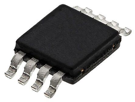
| 供应商器件封装 | 8-VSSOP |
| 共模抑制比—最小值 | 90 dB |
| 关闭 | Shutdown |
| 其它名称 | 296-28774-6 |
| 包装 | Digi-Reel® |
| 压摆率 | 10 V/µs |
| 商标 | Texas Instruments |
| 增益带宽生成 | 20 MHz |
| 增益带宽积 | 20MHz |
| 安装类型 | 表面贴装 |
| 安装风格 | SMD/SMT |
| 封装 | Reel |
| 封装/外壳 | 8-TSSOP,8-MSOP(0.118",3.00mm 宽) |
| 封装/箱体 | VSSOP-8 |
| 工作温度 | -40°C ~ 125°C |
| 工作电源电压 | 1.8 V to 5.5 V |
| 工厂包装数量 | 250 |
| 放大器类型 | 通用 |
| 最大工作温度 | + 125 C |
| 最小工作温度 | - 40 C |
| 标准包装 | 1 |
| 电压-电源,单/双 (±) | 1.8 V ~ 5.5 V, ±0.9 V ~ 2.75 V |
| 电压-输入失调 | 500µV |
| 电流-电源 | 1.5mA |
| 电流-输入偏置 | 0.2pA |
| 电流-输出/通道 | 65mA |
| 电源电流 | 1.75 mA |
| 电路数 | 2 |
| 系列 | OPA2322 |
| 设计资源 | http://www.digikey.com/product-highlights/cn/zh/texas-instruments-webench-design-center/3176 |
| 转换速度 | 10 V /us |
| 输入偏压电流—最大 | 10 pA |
| 输入补偿电压 | 2 mV |
| 输出电流 | 65 mA |
| 输出类型 | 满摆幅 |
| 通道数量 | 2 Channel |


- 商务部:美国ITC正式对集成电路等产品启动337调查
- 曝三星4nm工艺存在良率问题 高通将骁龙8 Gen1或转产台积电
- 太阳诱电将投资9.5亿元在常州建新厂生产MLCC 预计2023年完工
- 英特尔发布欧洲新工厂建设计划 深化IDM 2.0 战略
- 台积电先进制程称霸业界 有大客户加持明年业绩稳了
- 达到5530亿美元!SIA预计今年全球半导体销售额将创下新高
- 英特尔拟将自动驾驶子公司Mobileye上市 估值或超500亿美元
- 三星加码芯片和SET,合并消费电子和移动部门,撤换高东真等 CEO
- 三星电子宣布重大人事变动 还合并消费电子和移动部门
- 海关总署:前11个月进口集成电路产品价值2.52万亿元 增长14.8%


PDF Datasheet 数据手册内容提取
Product Sample & Technical Tools & Support & Folder Buy Documents Software Community OPA322,OPA322S OPA2322,OPA2322S OPA4322,OPA4322S SBOS538F–JANUARY2011–REVISEDDECEMBER2016 OPAx322x 20-MHz, Low-Noise, 1.8-V, RRI/O, CMOS Operational Amplifier With Shutdown 1 Features 3 Description • GainBandwidth:20MHz The OPAx322x series consists of single, dual, and 1 quad-channel CMOS operational amplifiers featuring • LowNoise:8.5nV√Hzat1kHz low noise and rail-to-rail inputs and outputs optimized • SlewRate:10V/μs for low-power, single-supply applications. Specified • LowTHD+N:0.0005% over a wide supply range of 1.8 V to 5.5 V, the low quiescent current of only 1.5 mA per channel makes • Rail-to-RailI/O these devices well-suited for power-sensitive • OffsetVoltage:2mV(maximum) applications. • SupplyVoltage:1.8Vto5.5V The combination of very low noise (8.5 nV√Hz at • SupplyCurrent:1.5mA/ch 1 kHz), high-gain bandwidth (20 MHz), and fast slew – Shutdown:0.1 μA/ch rate (10 V/μs) make the OPAx322x family ideal for a wide range of applications, including signal • Unity-GainStable conditioning and sensor amplification requiring high • SmallPackages: gains. Featuring low THD+N, the OPAx322x series is – SOT-23,SON,VSSOP,TSSOP also excellent for consumer audio applications, particularlyforsingle-supplysystems. 2 Applications The OPAx322S models include a shutdown mode • SensorSignalConditioning that allow the amplifiers to be switched from normal operation to a standby current that is typically less • ConsumerAudio than0.1μA. • Multi-PoleActiveFilters The OPA322 (single version) is available in 5-pin • Control-LoopAmplifiers SOT-23 and 6-pin SOT-23, while the OPA2322 (dual • Communications version) is offered in 8-pin VSSOP, 10-pin VSSOP, 8- • Security pin SOIC, and 8-pin SON packages. The quad versionOPA4322comesin14-pinTSSOPand16-pin • Scanners TSSOP packages. All versions are specified for operationfrom–40°Cto+125°C. Zero-CrossoverRail-to-RailInputStage EliminatesDistortion DeviceInformation(1) 1 PARTNUMBER PACKAGE BODYSIZE(NOM) 0.8 OPA322 SOT-23(5) 2.90mm×1.60mm 0.6 V) 0.4 OPA322S SOT-23(6) 2.90mm×1.60mm m e ( 0.2 SOIC(8) 4.90mm×3.91mm g a OPA2322 VSSOP(8) 3.00mm×3.00mm olt 0 et V -0.2 SON(8) 3.00mm×3.00mm Offs -0.4 OPA2322S VSSOP(10) 3.00mm×3.00mm -0.6 OPA4322 TSSOP(14) 5.00mm×4.40mm -0.8 RepreseVnta=tiv±e2 .U7n5i tVs OPA4322S TSSOP(16) 5.00mm×4.40mm S -1 (1) For all available packages, see the orderable addendum at -3 -2 -1 0 1 2 3 theendofthedatasheet. Common-Mode Voltage (V) 1 An IMPORTANT NOTICE at the end of this data sheet addresses availability, warranty, changes, use in safety-critical applications, intellectualpropertymattersandotherimportantdisclaimers.PRODUCTIONDATA.
OPA322,OPA322S OPA2322,OPA2322S OPA4322,OPA4322S SBOS538F–JANUARY2011–REVISEDDECEMBER2016 www.ti.com Table of Contents 1 Features.................................................................. 1 7.4 DeviceFunctionalModes........................................20 2 Applications........................................................... 1 8 ApplicationandImplementation........................ 21 3 Description............................................................. 1 8.1 ApplicationInformation............................................21 4 RevisionHistory..................................................... 2 8.2 TypicalApplication..................................................22 5 PinConfigurationandFunctions......................... 4 9 PowerSupplyRecommendations...................... 23 6 Specifications......................................................... 7 10 Layout................................................................... 24 6.1 AbsoluteMaximumRatings......................................7 10.1 LayoutGuidelines.................................................24 6.2 ESDRatings..............................................................7 10.2 LayoutExample ...................................................24 6.3 RecommendedOperatingConditions.......................7 11 DeviceandDocumentationSupport................. 25 6.4 ThermalInformation:OPA322,OPA322S................8 11.1 DeviceSupport......................................................25 6.5 ThermalInformation:OPA2322,OPA2322S............8 11.2 DocumentationSupport........................................26 6.6 ThermalInformation:OPA4322,OPA4322S............8 11.3 RelatedLinks........................................................26 6.7 ElectricalCharacteristics...........................................9 11.4 ReceivingNotificationofDocumentationUpdates26 6.8 TypicalCharacteristics............................................11 11.5 CommunityResources..........................................26 7 DetailedDescription............................................ 16 11.6 Trademarks...........................................................27 7.1 Overview.................................................................16 11.7 ElectrostaticDischargeCaution............................27 7.2 FunctionalBlockDiagram.......................................16 11.8 Glossary................................................................27 7.3 FeatureDescription.................................................16 12 Mechanical,Packaging,andOrderable Information........................................................... 27 4 Revision History NOTE:Pagenumbersforpreviousrevisionsmaydifferfrompagenumbersinthecurrentversion. ChangesfromRevisionE(June2012)toRevisionF Page • AddedESDRatingstable,FeatureDescriptionsection,DeviceFunctionalModes,ApplicationandImplementation section,PowerSupplyRecommendationssection,Layoutsection,DeviceandDocumentationSupportsection,and Mechanical,Packaging,andOrderableInformationsection.................................................................................................. 1 • Changeddevicepackagedescriptionstocurrentstandards................................................................................................. 1 • DeletedPackage/OrderingInformationtable;seePackageOptionAddendumattheendofthisdatasheet......................7 ChangesfromRevisionD(March2012)toRevisionE Page • ChangedproductstatusfromProductionDatatoMixedStatus............................................................................................ 1 • UpdatedDandDGKpinoutdrawing...................................................................................................................................... 5 • AddedFigure26toFigure29............................................................................................................................................... 15 • AddedShutdownFunctionsection....................................................................................................................................... 20 ChangesfromRevisionC(November2011)toRevisionD Page • ChangedproductstatusfromMixedStatustoProductionData............................................................................................ 1 • AddedOPA4322,OPA4322StotheInputBiasCurrent,Inputbiascurrent,OvertemperatureparameterinElectrical Characteristicstable............................................................................................................................................................... 9 • ChangedPowerSupply,OPA4322,OPA4322SOvertemperatureparametermaximumspecificationintheElectrical Characteristicstable............................................................................................................................................................. 10 ChangesfromRevisionB(July2011)toRevisionC Page • ChangedstatusofOPA2322SO-8(D)toproductiondatafromproductpreview................................................................. 1 2 SubmitDocumentationFeedback Copyright©2011–2016,TexasInstrumentsIncorporated ProductFolderLinks:OPA322OPA322S OPA2322 OPA2322SOPA4322 OPA4322S
OPA322,OPA322S OPA2322,OPA2322S OPA4322,OPA4322S www.ti.com SBOS538F–JANUARY2011–REVISEDDECEMBER2016 ChangesfromRevisionA(May2011)toRevisionB Page • AddedOPA322SthermalinformationtoOPA322ThermalInformationtable....................................................................... 8 • AddedOPA2322SthermalinformationtoOPA2322ThermalInformationtable................................................................... 8 • AddedOPA4322SthermalinformationtoOPA4322ThermalInformationtable................................................................... 8 • ChangedInputBiasCurrentInputbiascurrent,OvertemperatureparameterinElectricalCharacteristicstable.................9 • ChangedOpen-LoopGain,Open-loopvoltagegainparametertypicalspecificationintheElectricalCharacteristicstable.9 • ChangedOpen-LoopGain,PhasemarginparametertestconditionsintheElectricalCharacteristicstable........................9 • ChangedPowerSupply,QuiescentcurrentperamplifierOPA322/Sparametermaximumspecificationinthe ElectricalCharacteristics...................................................................................................................................................... 10 • ChangedPowerSupply,OPA322OvertemperatureparametermaximumspecificationintheElectrical Characteristicstable............................................................................................................................................................. 10 • ChangedPowerSupply,QuiescentcurrentperamplifierOPA4322/SparametertypicalspecificationintheElectrical Characteristics...................................................................................................................................................................... 10 • AddedtestconditionstoPowerSupplysectioninElectricalCharacteristicstable.............................................................. 10 • ChangedShutdown,Quiescentcurrent,peramplifierparametermaximumspecificationinElectricalCharacteristics table...................................................................................................................................................................................... 10 • UpdatedFigure1.................................................................................................................................................................. 11 • AddedFigure25................................................................................................................................................................... 15 • ChangedOverloadRecoveryTimesection.......................................................................................................................... 19 ChangesfromOriginal(January2011)toRevisionA Page • ChangeddocumentstatustoProductionData...................................................................................................................... 1 Copyright©2011–2016,TexasInstrumentsIncorporated SubmitDocumentationFeedback 3 ProductFolderLinks:OPA322OPA322S OPA2322 OPA2322SOPA4322 OPA4322S
OPA322,OPA322S OPA2322,OPA2322S OPA4322,OPA4322S SBOS538F–JANUARY2011–REVISEDDECEMBER2016 www.ti.com 5 Pin Configuration and Functions OPA322:DBVPackage OPA322S:DBVPackage 5-PinSOT-23 6-PinSOT-23 TopView TopView OUT 1 5 V+ VOUT 1 6 V+ V- 2 V- 2 5 SHDN +IN 3 4 -IN +IN 3 4 -IN PinFunctions:OPA322,OPA322S PIN OPA322 OPA322S I/O DESCRIPTION NAME SOT-23 SOT-23 –IN 4 4 I Invertinginput +IN 3 3 I Noninvertinginput OUT 1 1 O Output SHDN — 5 I Shutdowncontrol(activelow) V– 2 2 — Negative(lowest)powersupply V+ 5 6 — Positive(highest)powersupply 4 SubmitDocumentationFeedback Copyright©2011–2016,TexasInstrumentsIncorporated ProductFolderLinks:OPA322OPA322S OPA2322 OPA2322SOPA4322 OPA4322S
OPA322,OPA322S OPA2322,OPA2322S OPA4322,OPA4322S www.ti.com SBOS538F–JANUARY2011–REVISEDDECEMBER2016 OPA2322:DandDGKPackages OPA2322:DRGPackage 8-PinSOICandVSSOP 8-PinSON TopView TopView OUTA 1 8 V+ OUT A 1 8 V+ A Exposed -INA 2 7 OUTB -IN A 2 Thermal 7 OUT B +INA 3 B 6 -IN B +IN A 3 Dieo nPad 6 -IN B Underside V- 4 5 +IN B V- 4 5 +IN B (1) ConnectthermalpadtoV–. (2) Padsize:2mm×1.2mm. OPA2322S:DGSPackage 10-PinVSSOP TopView VOUT A 1 10 V+ -IN A 2 9 VOUT B A +IN A 3 8 -IN B B V- 4 7 +IN B SHDN A 5 6 SHDN B PinFunctions:OPA2322,OPA2322S PIN OPA2322 OPA2322S I/O DESCRIPTION NAME SOIC, SON VSSOP VSSOP –INA 2 2 2 I Invertinginput,channelA +INA 3 3 3 I Noninvertinginput,channelA –INB 6 6 8 I Invertinginput,channelB +INB 5 5 7 I Noninvertinginput,channelB OUTA 1 1 — O Output,channelA OUTB 7 7 — O Output,channelB SHDNA — — 5 I Shutdowncontrol,channelA(activelow) SHDNB — — 6 I Shutdowncontrol,channelB(activelow) V– 4 4 4 — Negative(lowest)powersupply V+ 8 8 10 — Positive(highest)powersupply VOUTA — — 1 O Output,channelA VOUTB — — 9 O Output,channelB Copyright©2011–2016,TexasInstrumentsIncorporated SubmitDocumentationFeedback 5 ProductFolderLinks:OPA322OPA322S OPA2322 OPA2322SOPA4322 OPA4322S
OPA322,OPA322S OPA2322,OPA2322S OPA4322,OPA4322S SBOS538F–JANUARY2011–REVISEDDECEMBER2016 www.ti.com PWPackage PWPackage 14-PinTSSOP 16-PinTSSOP TopView TopView OUT A 1 14 OUT D OUT A 1 16 OUT D A D A D -IN A 2 13 -IN D -IN A 2 15 -IN D +IN A 3 12 +IN D +IN A 3 14 +IN D V+ 4 11 V- V+ 4 13 V- +IN B 5 10 +IN C +IN B 5 12 +IN C -IN B 6 9 -IN C -IN B 6 11 -IN C B C B C OUT B 7 8 OUT C OUT B 7 10 OUT C SHDN A/B 8 9 SHDN C/D PinFunctions:OPA4322,OPA4322S PIN OPA4322 OPA4322S I/O DESCRIPTION NAME TSSOP TSSOP –INA 2 2 I Invertinginput,channelA +INA 3 3 I Noninvertinginput,channelA –INB 6 6 I Invertinginput,channelB +INB 5 5 I Noninvertinginput,channelB –INC 9 11 I Invertinginput,channelC +INC 10 12 I Noninvertinginput,channelC –IND 13 15 I Invertinginput,channelD +IND 12 14 I Noninvertinginput,channelD OUTA 1 1 O Output,channelA OUTB 7 7 O Output,channelB OUTC 8 10 O Output,channelC OUTD 14 16 O Output,channelD SHDNA/B — 8 I Shutdowncontrol,channelsAandB(activelow) SHDNC/D 9 I Shutdowncontrol,channelsCandD(activelow) V– 11 13 — Negative(lowest)powersupply V+ 4 4 — Positive(highest)powersupply 6 SubmitDocumentationFeedback Copyright©2011–2016,TexasInstrumentsIncorporated ProductFolderLinks:OPA322OPA322S OPA2322 OPA2322SOPA4322 OPA4322S
OPA322,OPA322S OPA2322,OPA2322S OPA4322,OPA4322S www.ti.com SBOS538F–JANUARY2011–REVISEDDECEMBER2016 6 Specifications 6.1 Absolute Maximum Ratings overoperatingfree-airtemperaturerange(unlessotherwisenoted)(1) MIN MAX UNIT Supplyvoltage,V =(V+)–(V–) 6 V S Voltage Signalinputpins(2) (V–)–0.5 (V+)+0.5 V Signalinputpins(2) –10 10 mA Current Outputshort-circuit(3) Continuous Operating,T –40 150 °C A Temperature Junction,T 150 °C J Storage,T –65 150 °C stg (1) StressesbeyondthoselistedunderAbsoluteMaximumRatingsmaycausepermanentdamagetothedevice.Thesearestressratings only,whichdonotimplyfunctionaloperationofthedeviceattheseoranyotherconditionsbeyondthoseindicatedunderRecommended OperatingConditions.Exposuretoabsolute-maximum-ratedconditionsforextendedperiodsmayaffectdevicereliability. (2) Inputterminalsarediode-clampedtothepower-supplyrails.Inputsignalsthatcanswingmorethan0.5Vbeyondthesupplyrailsmust becurrentlimitedto10mAorless. (3) Short-circuittoground,oneamplifierperpackage. 6.2 ESD Ratings VALUE UNIT Human-bodymodel(HBM),perANSI/ESDA/JEDECJS-001(1) ±4000 V Electrostatic Charged-devicemodel(CDM),perJEDECspecificationJESD22-C101(2) ±1000 V (ESD) discharge Machinemodel(MM) ±200 (1) JEDECdocumentJEP155statesthat500-VHBMallowssafemanufacturingwithastandardESDcontrolprocess. (2) JEDECdocumentJEP157statesthat250-VCDMallowssafemanufacturingwithastandardESDcontrolprocess. 6.3 Recommended Operating Conditions overoperatingfree-airtemperaturerange(unlessotherwisenoted) MIN MAX UNIT V Specifiedvoltage 1.8 5.5 V S T Specifiedtemperature –40 125 °C A Copyright©2011–2016,TexasInstrumentsIncorporated SubmitDocumentationFeedback 7 ProductFolderLinks:OPA322OPA322S OPA2322 OPA2322SOPA4322 OPA4322S
OPA322,OPA322S OPA2322,OPA2322S OPA4322,OPA4322S SBOS538F–JANUARY2011–REVISEDDECEMBER2016 www.ti.com 6.4 Thermal Information: OPA322, OPA322S OPA322 OPA322S THERMALMETRIC(1) DBV(SOT-23) DBV(SOT-23) UNITS 5PINS 6PINS RθJA Junction-to-ambientthermalresistance 219.3 177.5 °C/W RθJC(top) Junction-to-case(top)thermalresistance 107.5 108.9 °C/W RθJB Junction-to-boardthermalresistance 57.5 27.4 °C/W ψJT Junction-to-topcharacterizationparameter 7.4 13.3 °C/W ψJB Junction-to-boardcharacterizationparameter 56.9 26.9 °C/W RθJC(bot) Junction-to-case(bottom)thermalresistance — — °C/W (1) Formoreinformationabouttraditionalandnewthermalmetrics,seetheSemiconductorandICPackageThermalMetricsapplication report. 6.5 Thermal Information: OPA2322, OPA2322S OPA2322 OPA2322S THERMALMETRIC(1) D(SOIC) DRG(SON) DGK(VSSOP) DGS (VSSOP) 8PINS 8PINS 8PINS 10PINS UNITS RθJA Junction-to-ambientthermalresistance 122.6 50.6 174.8 171.5 °C/W RθJC(top) Junction-to-case(top)thermalresistance 67.1 54.9 43.9 43 °C/W RθJB Junction-to-boardthermalresistance 64 25.2 95 91.4 °C/W ψJT Junction-to-topcharacterizationparameter 13.2 0.6 2 1.9 °C/W ψJB Junction-to-boardcharacterizationparameter 63.4 25.3 93.5 89.9 °C/W RθJC(bot) Junction-to-case(bottom)thermalresistance — 5.7 — — °C/W (1) Formoreinformationabouttraditionalandnewthermalmetrics,seetheSemiconductorandICPackageThermalMetricsapplication report. 6.6 Thermal Information: OPA4322, OPA4322S OPA4322 OPA4322S THERMALMETRIC(1) PW(TSSOP) PW(TSSOP) 14PINS 16PINS UNITS RθJA Junction-to-ambientthermalresistance 109.8 105.9 °C/W RθJC(top) Junction-to-case(top)thermalresistance 34.9 28.1 °C/W RθJB Junction-to-boardthermalresistance 52.5 51.1 °C/W ψJT Junction-to-topcharacterizationparameter 2.2 0.8 °C/W ψJB Junction-to-boardcharacterizationparameter 51.8 50.4 °C/W RθJC(bot) Junction-to-case(bottom)thermalresistance — — °C/W (1) Formoreinformationabouttraditionalandnewthermalmetrics,seetheSemiconductorandICPackageThermalMetricsapplication report. 8 SubmitDocumentationFeedback Copyright©2011–2016,TexasInstrumentsIncorporated ProductFolderLinks:OPA322OPA322S OPA2322 OPA2322SOPA4322 OPA4322S
OPA322,OPA322S OPA2322,OPA2322S OPA4322,OPA4322S www.ti.com SBOS538F–JANUARY2011–REVISEDDECEMBER2016 6.7 Electrical Characteristics AtV =1.8Vto5.5V,or±0.9Vto±2.75V,T =25°C,R =10kΩconnectedtoV /2,V =V /2,V =V /2,and S A L S CM S OUT S SHDN_x=V +(unlessotherwisenoted). S PARAMETER TESTCONDITIONS MIN TYP MAX UNIT OFFSETVOLTAGE VOS Inputoffsetvoltage 0.5 2 mV dVOS/dT vstemperature VS=5.5V 1.8 6 μV/°C TA=25°C 10 50 PSR vspowersupply VS=1.8Vto5.5V μV/V TA=–40°Cto125°C 20 65 Channelseparation At1kHz 130 dB INPUTVOLTAGE Common-modevoltage VCM range (V–)–0.1 (V+)+0.1 V Common-moderejection TA=25°C 90 100 CMRR ratio (V–)–0.1V<VCM<(V+)+0.1V TA=–40°Cto125°C 90 dB INPUTBIASCURRENT TA=25°C ±0.2 ±10 TA=–40°Cto85°C ±50 IB Inputbiascurrent OPA322andOPA322S,TA=–40°Cto125°C ±800 pA OPA2322andOPA2322S,TA=–40°Cto125°C ±400 OPA4322andOPA4322S,TA=–40°Cto125°C ±400 TA=25°C ±0.2 ±10 IOS Inputoffsetcurrent TA=–40°Cto85°C ±50 pA TA=–40°Cto125°C ±400 NOISE Inputvoltagenoise f=0.1Hzto10Hz 2.8 μVPP f=1kHz 8.5 en Inputvoltagenoisedensity nV/√Hz f=10kHz 7 in Inputcurrentnoisedensity f=1kHz 0.6 fA/√Hz INPUTCAPACITANCE Differential 5 pF Common-mode 4 pF OPEN-LOOPGAIN 0.1V<VO<(V+)–0.1V,RL=10kΩ 100 130 AOL Open-loopvoltagegain dB 0.1V<VO<(V+)–0.1V,RL=10kΩ 94 PM Phasemargin VS=5V,CL=50pF 47 ° FREQUENCYRESPONSE GBP Gainbandwidthproduct VS=5V,CL=50pF,unitygain 20 MHz SR Slewrate VS=5V,CL=50pF,G=+1 10 V/μs VS=5V,CL=50pF,to0.1%,2-Vstep,G=+1 0.25 tS Settlingtime μs VS=5V,CL=50pF,to0.01%,2-Vstep,G=+1 0.32 Overloadrecoverytime VS=5V,CL=50pF,VIN×G>VS 100 ns VS=5V,CL=50pF,VO=4VPP,G=+1,f=10kHz, 0.0005% Totalharmonicdistortion+ RL=10kΩ THD+N noise(1) VS=5V,CL=50pF,VO=2VPP,G=+1,f=10kHz, 0.0011% RL=600Ω (1) Third-orderfilter;bandwidth=80kHzat–3dB Copyright©2011–2016,TexasInstrumentsIncorporated SubmitDocumentationFeedback 9 ProductFolderLinks:OPA322OPA322S OPA2322 OPA2322SOPA4322 OPA4322S
OPA322,OPA322S OPA2322,OPA2322S OPA4322,OPA4322S SBOS538F–JANUARY2011–REVISEDDECEMBER2016 www.ti.com Electrical Characteristics (continued) AtV =1.8Vto5.5V,or±0.9Vto±2.75V,T =25°C,R =10kΩconnectedtoV /2,V =V /2,V =V /2,and S A L S CM S OUT S SHDN_x=V +(unlessotherwisenoted). S PARAMETER TESTCONDITIONS MIN TYP MAX UNIT OUTPUT Voltageoutput(swingfrom TA=25°C 10 20 VO bothrails) RL=10kΩ TA=–40°Cto125°C 30 mV ISC Short-circuitcurrent VS=5.5V ±65 mA CL Capacitiveloaddrive SeeTypicalCharacteristics RO Open-loopoutputresistance IO=0mA,f=1MHz 90 Ω POWERSUPPLY VS Specifiedvoltagerange 1.8 5.5 V OPA322andOPA322S, TA=25°C 1.6 1.9 IO=0mA,VS=5.5V TA=–40°Cto125°C 2 Quiescentcurrentper OPA2322andOPA2322S, TA=25°C 1.5 1.75 IQ amplifier IO=0mA,VS=5.5V TA=–40°Cto125°C 1.85 mA OPA4322andOPA4322S, TA=25°C 1.4 1.65 IO=0mA,VS=5.5V TA=–40°Cto125°C 1.75 Power-ontime VS+=0Vto5V,to90%IQlevel 28 μs SHUTDOWN(2) Quiescentcurrent IQSD (peramplifier) VS=1.8Vto5.5V,allamplifiersdisabled,SHDN=VS– 0.1 0.5 µA VIH Highvoltage(enabled) VS=1.8Vto5.5V,amplifierenabled (V+)–0.1 V VIL Lowvoltage(disabled) VS=1.8Vto5.5V,amplifierdisabled (V–)+0.1 V A(fumllpslihfiuetrdeonwanb)l(e3)time VVSOU=T1=.80.V9t×oV5S.5/2V(4,)fullshutdown;G=1, 10 µs tON A(pmarptliiafilesrheuntdaobwlent)im(3)e VVSOU=T1=.80.V9t×oV5S.5/2V(4,)partialshutdown;G=1, 6 µs tOFF Amplifierdisabletime(3) VS=1.8Vto5.5V,G=1,VOUT=0.1×VS/2 3 µs SHDNpininputbiascurrent VS=1.8Vto5.5V,VIH=5V 0.13 µA (perpin) VS=1.8Vto5.5V,VIL=0V 0.04 (2) Ensuredbydesignandcharacterization;notproductiontested. (3) Disabletime(t )andenabletime(t )aredefinedasthetimeintervalbetweenthe50%pointofthesignalappliedtotheSHDNpin OFF ON andthepointatwhichtheoutputvoltagereachesthe10%(disable)or90%(enable)level. (4) FullshutdownreferstothedualOPA2322ShavingbothchannelsAandBdisabled(SHDN_A=SHDN_B=V )andthequad S– OPA4322ShavingallchannelsAtoDdisabled(SHDN_A/B=SHDN_C/D=V ).Forpartialshutdown,onlyoneSHDNpinisexercised; S– inthismode,theinternalbiasingandoscillatorremainoperationalandtheenabletimeisshorter. 10 SubmitDocumentationFeedback Copyright©2011–2016,TexasInstrumentsIncorporated ProductFolderLinks:OPA322OPA322S OPA2322 OPA2322SOPA4322 OPA4322S
OPA322,OPA322S OPA2322,OPA2322S OPA4322,OPA4322S www.ti.com SBOS538F–JANUARY2011–REVISEDDECEMBER2016 6.8 Typical Characteristics AtT =25°C,V =V =mid-supply,andR =10kΩ(unlessotherwisenoted). A CM OUT L 140 -20 125 R = 10 kW, 50 pF L 120 V =±2.5 V -40 120 S 10 kWLoad 100 -60 B) 115 d 80 -80 n ( 110 Gain (dB) 6400 --110200 Phase ()° n-Loop Gai 110050 2 kWLoad e p 20 -140 O 95 0 Gain -160 90 Phase -20 -180 85 1 10 100 1k 10k 100k 1M 10M 100M -50 -25 0 25 50 75 100 125 150 Frequency (Hz) Temperature (°C) Figure1.Open-LoopGainandPhasevsFrequency Figure2.Open-LoopGainvsTemperature 1 6 0.8 5 4 0.6 A) A) 3 nt (p 0.4 nt (p 2 urre 0.2 urre 1 C 0 C 0 Bias -0.2 Bias -1 Input ---000...468 IIB- Input ----2345 IIIBB+- B+ OS -1 -6 0.9 1.1 1.3 1.5 1.7 1.9 2.1 2.3 2.5 2.7 2.9 -3 -2.5 -2 -1.5 -1 -0.5 0 0.5 1 1.5 2 2.5 3 Supply Voltage (±V) Common-Mode Voltage (V) Figure3.InputBiasCurrentvsSupplyVoltage Figure4.InputBiasCurrent vsCommon-ModeVoltage 1300 1.6 1200 IOS pA) 11109000000 IIBB+- A/Ch) 1.55 Input Bias Current ( 876543210000000000000000 IB IOS Quiescent Current (m 11..1143..5554 +++1822555°°CC°C 0 -40°C -100 1.3 -50 -25 0 25 50 75 100 125 150 1.5 2 2.5 3 3.5 4 4.5 5 5.5 Temperature (°C) Supply Voltage (V) Figure5.InputBiasCurrentvsTemperature Figure6.QuiescentCurrentvsSupplyVoltage Copyright©2011–2016,TexasInstrumentsIncorporated SubmitDocumentationFeedback 11 ProductFolderLinks:OPA322OPA322S OPA2322 OPA2322SOPA4322 OPA4322S
OPA322,OPA322S OPA2322,OPA2322S OPA4322,OPA4322S SBOS538F–JANUARY2011–REVISEDDECEMBER2016 www.ti.com Typical Characteristics (continued) AtT =25°C,V =V =mid-supply,andR =10kΩ(unlessotherwisenoted). A CM OUT L 14 1 0.8 12 %) 0.6 s ( 10 V) 0.4 er m mplifi 8 age ( 0.2 er of A 6 et Volt -0.02 b s um 4 Off -0.4 N 2 -0.6 -0.8 RepreseVnta=tiv±e2 .U7n5i tVs 0 S -1 -1.5 -1.3 -1.1 -0.9 -0.7 -0.5 -0.3 -0.1 0.1 0.3 0.5 0.7 0.9 1.1 1.3 1.5 -3 -2 -1 0 1 2 3 Common-Mode Voltage (V) Offset Voltage (mV) Figure7.OffsetVoltageProductionHistogram Figure8.OffsetVoltagevsCommon-ModeVoltage 1000 6 V = 1.8 V to 5.5 V S 5 4 )z Öoltage Noise (nV/H 10100 mVoltage (V) -32101 V -2 -3 1 -4 10 100 1 k 10 k 100 k 1 M 0 1 2 3 4 5 6 7 8 9 10 Frequency (Hz) Time (s) Figure9.InputVoltageNoiseSpectralDensity Figure10.0.1-Hzto10-HzInputVoltageNoise vsFrequency 60 60 V = +1.8 V V = +5.5 V S S R = 10 kW R = 10 kW L L G = +100 V/V C = 50 pF G = +100 V/V C = 50 pF 40 L 40 L B) B) d d n ( 20 n ( 20 ai G = +10 V/V ai G = +10 V/V G G 0 0 G = +1 V/V G = +1 V/V -20 -20 10 k 100 k 1 M 10 M 100 M 10 k 100 k 1 M 10 M 100 M Frequency (Hz) Frequency (Hz) Figure11.Closed-LoopGainvsFrequency Figure12.Closed-LoopGainvsFrequency 12 SubmitDocumentationFeedback Copyright©2011–2016,TexasInstrumentsIncorporated ProductFolderLinks:OPA322OPA322S OPA2322 OPA2322SOPA4322 OPA4322S
OPA322,OPA322S OPA2322,OPA2322S OPA4322,OPA4322S www.ti.com SBOS538F–JANUARY2011–REVISEDDECEMBER2016 Typical Characteristics (continued) AtT =25°C,V =V =mid-supply,andR =10kΩ(unlessotherwisenoted). A CM OUT L 6 3 5.5 V S 5 2 e (V)PP 4 3.3 VS ge (V) 1 -40°C ut Voltag 3 put Volta 0 ++21525°C°C utp 2 Out -1 O 1.8 V S 1 R = 10 kW -2 L CL= 50 pF VS=±2.75 V 0 -3 10 k 100 k 1 M 10 M 0 10 20 30 40 50 60 70 80 Frequency (Hz) Output Current (mA) Figure13.MaximumOutputVoltagevsFrequency Figure14.OutputVoltageSwingvsOutputCurrent 1000 70 VS= ±2.75 V G = 1, VS= 1.8 V 60 G = 1, V = 5.5 V S G = 10, V = 1.8 V 50 S W) %) G = 10, VS= 5.5 V ce ( ot ( 40 an 100 ho mped Overs 30 I 20 10 10 0 1 10 100 1 k 10 k 100 k 1 M 10 M 100 M 0 500 1000 1500 2000 2500 3000 Frequency (Hz) Capacitive Load (pF) Figure15.Open-LoopOutputImpedance Figure16.Small-SignalOvershoot vsFrequency vsLoadCapacitance %) 0.1 %) 0.1 Frequency = 10 kHz Noise ( Noise ( VVISN== ±22 V.5P PV d d G = +1 V/V an 0.01 an 0.01 n n Distortio Load = 600W Distortio Load = 600W nic 0.001 nic 0.001 o o m m ar Frequency = 10 kHz ar al H VS=±2.5 V Load = 10 kW al H Load = 10 kW Tot G = +1 V/V Tot 0.0001 0.0001 0.01 0.1 1 10 10 100 1 k 10 k 100 k V (V ) Frequency (Hz) IN PP Figure17.THD+NvsAmplitude Figure18.THD+NvsFrequency Copyright©2011–2016,TexasInstrumentsIncorporated SubmitDocumentationFeedback 13 ProductFolderLinks:OPA322OPA322S OPA2322 OPA2322SOPA4322 OPA4322S
OPA322,OPA322S OPA2322,OPA2322S OPA4322,OPA4322S SBOS538F–JANUARY2011–REVISEDDECEMBER2016 www.ti.com Typical Characteristics (continued) AtT =25°C,V =V =mid-supply,andR =10kΩ(unlessotherwisenoted). A CM OUT L 0.1 0 %) Frequency = 10 kHz V =±2.75 V se ( VIN= 4 VPP -20 S Noi VS=±2.5 V B) on and 0.01 G = +1 V/V ation (d --4600 orti Load = 600W par monic Dist 0.001 hannel Se -1-0800 ar C al H Load = 10 kW -120 Tot 0.0001 -140 10 100 1 k 10 k 100 k 1 k 10 k 100 k 1 M 10 M 100 M Frequency (Hz) Frequency (Hz) Figure19.THD+NvsFrequency Figure20.ChannelSeparation vsFrequency(forDual) 12 0.1 C = 50 pF Gain = +1 L 0.075 VS=±2.75 V 11.5 V = 100 mV IN PP 0.05 s) 11 mV/ Rise V) 0.025 Slew Rate ( 101.50 Fall Voltage ( -0.0250 -0.05 9.5 -0.075 VOUT V IN 9 -0.1 1.6 2 2.4 2.8 3.2 3.6 4 4.4 4.8 5.2 5.6 -0.8 -0.4 0 0.4 0.8 1.2 1.6 Supply Voltage (V) Time (ms) Figure21.SlewRatevsSupplyVoltage Figure22.Small-SignalStepResponse 0.1 1.5 Gain = +1 0.075 1 VS=±2.75 V V = 2 V 0.05 V IN PP IN 0.5 V) 0.025 Gain =-1 V) V e ( VS=±2.75 V e ( OUT oltag 0 VIN= 100 mVPP oltag 0 V -0.025 V -0.5 -0.05 -0.075 VOUT -1 V IN -0.1 -1.5 -1.6 -1.2 -0.8 -0.4 0 0.4 0.8 -0.4 0 0.4 0.8 1.2 1.6 Time (ms) Time (ms) Figure23.Small-SignalStepResponse Figure24.Large-SignalStepResponsevsTime 14 SubmitDocumentationFeedback Copyright©2011–2016,TexasInstrumentsIncorporated ProductFolderLinks:OPA322OPA322S OPA2322 OPA2322SOPA4322 OPA4322S
OPA322,OPA322S OPA2322,OPA2322S OPA4322,OPA4322S www.ti.com SBOS538F–JANUARY2011–REVISEDDECEMBER2016 Typical Characteristics (continued) AtT =25°C,V =V =mid-supply,andR =10kΩ(unlessotherwisenoted). A CM OUT L 120 3 Shutdown Signal Common-Mode Rejection Ratio,ower-Supply Rejection Ratio (dB) 10864200000 PSRR Voltage (V) −−−0112110.......82606284 Output Signal P CMRR −2.4 0 −3 100 1k 10k 100k 1M 0 2 4 6 8 10 12 14 16 18 20 Frequency (Hz) Time (µs) G000 Figure25.CMRRandPSRRvsFrequency Figure26.TurnoffTransient 3 5 4.5 Shutdown Signal 2.4 4 3.5 Output Signal 1.8 3 2.5 1.2 2 1.5 Voltage (V) −00..066 Voltage (V) −−100−...515051 −2 −1.2 −2.5 −3 −1.8 −3.5 Shutdown Signal −4 −2.4 −4.5 Output Signal −5 −3 0 200 400 600 800 100012001400160018002000 0 2 4 6 8 10 12 14 16 18 20 Time (µs) Time (µs) G000 G000 5.5V(HighSupply) Figure27.TurnonTransient Figure28.TurnonandTurnoffTransient 2 1.5 1 V) 0.5 e ( g 0 a olt V −0.5 −1 −1.5 Shutdown Signal Output Signal −2 0 200 400 600 800 100012001400160018002000 Time (µs) G000 1.8V(LowSupply) Figure29.TurnonandTurnoffTransient Copyright©2011–2016,TexasInstrumentsIncorporated SubmitDocumentationFeedback 15 ProductFolderLinks:OPA322OPA322S OPA2322 OPA2322SOPA4322 OPA4322S
OPA322,OPA322S OPA2322,OPA2322S OPA4322,OPA4322S SBOS538F–JANUARY2011–REVISEDDECEMBER2016 www.ti.com 7 Detailed Description 7.1 Overview The OPA322 family of operational amplifiers (op amps) are high-speed, precision amplifiers perfectly suited to drive 12-, 14-, and 16-bit analog-to-digital converters. Low-output impedance with flat frequency characteristics and zero-crossover distortion circuitry enable high linearity over the full input common-mode range, achieving truerail-to-railinputfroma1.8-Vto5.5-Vsinglesupply. 7.2 Functional Block Diagram V+ Low Noise Charge Pump Bias Circuitry +IN -IN OUT Input Stage Load Bias Circuitry V- Copyright © 2016, Texas Instruments Incorporated 7.3 Feature Description 7.3.1 OperatingVoltage TheOPA322seriesopampsareunity-gainstableandcanoperateonasingle-supplyvoltage(1.8Vto5.5V),or a split-supply voltage (±0.9 V to ±2.75 V), making them highly versatile and easy to use. The power-supply pins must have local bypass ceramic capacitors (typically 0.001 μF to 0.1 μF). These amplifiers are fully specified from 1.8 V to 5.5 V and over the extended temperature range of –40°C to 125°C. Parameters that can exhibit variancewithregardtooperatingvoltageortemperaturearepresentedintheTypicalCharacteristics. 7.3.2 InputandESDProtection The OPA322 incorporates internal electrostatic discharge (ESD) protection circuits on all pins. In the case of input and output pins, this protection primarily consists of current-steering diodes connected between the input and power-supply pins. These ESD protection diodes also provide in-circuit input overdrive protection, as long as the current is limited to 10 mA as stated in the Absolute Maximum Ratings. Many input signals are inherently current-limited to less than 10 mA; therefore, a limiting resistor is not required. Figure 30 shows how a series input resistor (R ) may be added to the driven input to limit the input current. The added resistor contributes S thermalnoiseattheamplifierinputandthevaluemustbekepttotheminimuminnoise-sensitiveapplications. 16 SubmitDocumentationFeedback Copyright©2011–2016,TexasInstrumentsIncorporated ProductFolderLinks:OPA322OPA322S OPA2322 OPA2322SOPA4322 OPA4322S
OPA322,OPA322S OPA2322,OPA2322S OPA4322,OPA4322S www.ti.com SBOS538F–JANUARY2011–REVISEDDECEMBER2016 Feature Description (continued) V+ I OVERLOAD 10 mA, Max OPA322 VOUT V IN R S Copyright © 2016,Texas Instruments Incorporated Figure30. InputCurrentProtection 7.3.3 PhaseReversal The OPA322 op amps are designed to be immune to phase reversal when the input pins exceed the supply voltages, therefore providing further in-system stability and predictability. Figure 31 shows the input voltage exceedingthesupplyvoltagewithoutanyphasereversal. 4 V =±2.5 V V S IN 3 2 V OUT V) 1 e ( g 0 a olt V -1 -2 -3 -4 -500 -250 0 250 500 750 1000 Time (ms) Figure31. NoPhaseReversal 7.3.4 FeedbackCapacitorImprovesResponse For optimum settling time and stability with high-impedance feedback networks, it may be necessary to add a feedback capacitor across the feedback resistor, R , as shown in Figure 32. This capacitor compensates for the F zero created by the feedback network impedance and the OPA322 input capacitance (and any parasitic layout capacitance).Theeffectbecomesmoresignificantwithhigherimpedancenetworks. C F R R IN F V IN V+ C IN R ´C = R ´C IN IN F F OPA322 V OUT C L C IN Copyright © 2016,Texas Instruments Incorporated NOTE:WhereC isequaltotheOPA322inputcapacitance(approximately9pF)plusanyparasiticlayoutcapacitance. IN Figure32. FeedbackCapacitorImprovesDynamicPerformance Copyright©2011–2016,TexasInstrumentsIncorporated SubmitDocumentationFeedback 17 ProductFolderLinks:OPA322OPA322S OPA2322 OPA2322SOPA4322 OPA4322S
OPA322,OPA322S OPA2322,OPA2322S OPA4322,OPA4322S SBOS538F–JANUARY2011–REVISEDDECEMBER2016 www.ti.com Feature Description (continued) For the circuit shown in Figure 32, the value of the variable feedback capacitor must be chosen so that the input resistance times the input capacitance of the OPA322 (typically 9 pF) plus the estimated parasitic layout capacitanceequalsthefeedbackcapacitortimesthefeedbackresistorwithEquation1. R ×C =R ×C IN IN F F where • C isequaltotheOPA322inputcapacitance(sumofdifferentialandcommon-mode)plusthelayout IN capacitance (1) Thecapacitorvaluecanbeadjusteduntiloptimumperformanceisobtained. 7.3.5 EMISusceptibilityandInputFiltering Operational amplifiers vary in susceptibility to electromagnetic interference (EMI). If conducted EMI enters the device,theDCoffsetobservedattheamplifieroutputmayshiftfromthenominalvaluewhileEMIispresent.This shift is a result of signal rectification associated with the internal semiconductor junctions. While all operational amplifier pin functions can be affected by EMI, the input pins are likely to be the most susceptible. The OPA322 operational amplifier family incorporates an internal input low-pass filter that reduces the amplifier response to EMI.Bothcommon-modeanddifferentialmodefilteringareprovidedbytheinputfilter.Thefilterisdesignedfora cutofffrequencyofapproximately580MHz(–3dB),witharoll-offof20dBperdecade. 7.3.6 OutputImpedance The open-loop output impedance of the OPA322 common-source output stage is approximately 90 Ω. When the op amp is connected with feedback, this value is reduced significantly by the loop gain. For each decade rise in the closed-loop gain, the loop gain is reduced by the same amount, which results in a tenfold increase in effective output impedance. While the OPA322 output impedance remains very flat over a wide frequency range, at higher frequencies the output impedance rises as the open-loop gain of the op amp drops. However, at these frequencies the output also becomes capacitive as a result of parasitic capacitance. This characteristic, in turn, prevents the output impedance from becoming too high, which can cause stability problems when driving large capacitive loads. As mentioned previously, the OPA322 has excellent capacitive load drive capability for an op ampwithitsbandwidth. 7.3.7 CapacitiveLoadandStability The OPA322 is designed to be used in applications where driving a capacitive load is required. As with all op amps, there may be specific instances where the OPA322 can become unstable. The particular op amp circuit configuration, layout, gain, and output loading are some of the factors to consider when establishing whether an amplifier is stable in operation. An op amp in the unity-gain (+1-V/V) buffer configuration and driving a capacitive load exhibits a greater tendency to become unstable than an amplifier operated at a higher noise gain. The capacitive load, in conjunction with the op amp output resistance, creates a pole within the feedback loop that degrades the phase margin. The degradation of the phase margin increases as the capacitive loading increases. When operating in the unity-gain configuration, the OPA322 remains stable with a pure capacitive load up to approximately1nF. The equivalent series resistance (ESR) of some very large capacitors (C > 1 µF) is sufficient to alter the phase L characteristics in the feedback loop such that the amplifier remains stable. Increasing the amplifier closed-loop gain allows the amplifier to drive increasingly larger capacitance. This increased capability is evident when observing the overshoot response of the amplifier at higher voltage gains, as shown in Figure 33. One technique for increasing the capacitive load drive capability of the amplifier operating in unity gain is to insert a small resistor(R ),typically10Ω to20Ω,inserieswiththeoutput,asshowninFigure34. S This resistor significantly reduces the overshoot and ringing associated with large capacitive loads. A possible problem with this technique is that a voltage divider is created with the added series resistor and any resistor connected in parallel with the capacitive load. The voltage divider introduces a gain error at the output that reduces the output swing. The error contributed by the voltage divider, however, may be insignificant. For instance,withaloadresistance,R =10kΩandR =20 Ω,thegainerrorisonlyabout0.2%.However,whenR L S L isdecreasedto600Ω,whichtheOPA322isabletodrive,theerrorincreasesto7.5%. 18 SubmitDocumentationFeedback Copyright©2011–2016,TexasInstrumentsIncorporated ProductFolderLinks:OPA322OPA322S OPA2322 OPA2322SOPA4322 OPA4322S
OPA322,OPA322S OPA2322,OPA2322S OPA4322,OPA4322S www.ti.com SBOS538F–JANUARY2011–REVISEDDECEMBER2016 Feature Description (continued) 70 G = 1, V = 1.8 V S 60 G = 1, V = 5.5 V S G = 10, V = 1.8 V 50 S %) G = 10, VS= 5.5 V ot ( 40 o h ers 30 v O 20 10 0 0 500 1000 1500 2000 2500 3000 Capacitive Load (pF) Figure33. Small-SignalOvershootvsCapacitiveLoad(100-mV OutputStep) PP V+ R S OPA322 VOUT V 10Wto IN 20W RL CL Copyright © 2016,Texas Instruments Incorporated Figure34. ImprovingCapacitiveLoadDrive 7.3.8 OverloadRecoveryTime Overload recovery time is the time required for the output of the amplifier to come out of saturation and recover to the linear region. Overload recovery is particularly important in applications where small signals must be amplified in the presence of large transients. Figure 35 and Figure 36 show the positive and negative overload recovery times of the OPA322, respectively. In both cases, the time elapsed before the OPA322 comes out of saturationislessthan100ns.Inaddition,thesymmetrybetweenthepositiveandnegativerecoverytimesallows excellentsignalrectificationwithoutdistortionoftheoutputsignal. spacer 3 1 V =±2.75 V S 2.5 G =-10 0.5 Output Input 2 0 V) 1.5 V) -0.5 ge ( 1 ge ( -1 a a Volt 0.5 Volt -1.5 0 -2 Input Output -0.5 -2.5 VS=±2.75 V G =-10 -1 -3 9.75 10 10.25 10.5 10.75 11 9.75 10 10.25 10.5 10.75 11 Time (250 ns/div) Time (250 ns/div) Figure35.PositiveRecoveryTime Figure36.NegativeRecoveryTime Copyright©2011–2016,TexasInstrumentsIncorporated SubmitDocumentationFeedback 19 ProductFolderLinks:OPA322OPA322S OPA2322 OPA2322SOPA4322 OPA4322S
OPA322,OPA322S OPA2322,OPA2322S OPA4322,OPA4322S SBOS538F–JANUARY2011–REVISEDDECEMBER2016 www.ti.com Feature Description (continued) 7.3.9 ShutdownFunction The SHDN (enable) pin function of the OPAx322S is referenced to the negative supply voltage of the operational amplifier.Alogiclevelhighenablestheopamp.Avalidlogichighisdefinedasvoltage[(V+) – 0.1V],upto(V+), applied to the SHDN pin. A valid logic low is defined as [(V–) + 0.1 V], down to (V–), applied to the enable pin. The maximum allowed voltage applied to SHDN is 5.5 V with respect to the negative supply, independent of the positive supply voltage. This pin must either be connected to a valid high or a low voltage or driven, and not left asanopencircuit. The logic input is a high-impedance CMOS input. Dual op amp versions are independently controlled and quad op amp versions are controlled in pairs with logic inputs. For battery-operated applications, this feature may be used to greatly reduce the average current and extend battery life. The enable time is 10 µs for full shutdown of all channels; disable time is 3 μs. When disabled, the output assumes a high-impedance state. This architecture allows the OPAx322S to be operated as a gated amplifier (or to have the device output multiplexed onto a common analog output bus). Shutdown time (t ) depends on loading conditions and increases with increased OFF load resistance. To ensure shutdown (disable) within a specific shutdown time, the specified 10-kΩ load to mid- supply (V / 2) is required. If using the OPAx322S without a load, the resulting turnoff time is significantly S increased. 7.4 Device Functional Modes The OPA322 family of operational amplifiers are operational when power-supply voltages between 1.8 V to 5.5 V are applied. Devices with an S suffix have a shutdown capability. For a detailed description of the shutdown function,refertoShutdownFunction. 20 SubmitDocumentationFeedback Copyright©2011–2016,TexasInstrumentsIncorporated ProductFolderLinks:OPA322OPA322S OPA2322 OPA2322SOPA4322 OPA4322S
OPA322,OPA322S OPA2322,OPA2322S OPA4322,OPA4322S www.ti.com SBOS538F–JANUARY2011–REVISEDDECEMBER2016 8 Application and Implementation NOTE Information in the following applications sections is not part of the TI component specification, and TI does not warrant its accuracy or completeness. TI’s customers are responsible for determining suitability of components for their purposes. Customers should validateandtesttheirdesignimplementationtoconfirmsystemfunctionality. 8.1 Application Information The OPA322 family offers outstanding DC and AC performance. These devices operate up to a 5.5-V power supply and offer ultra-low input bias current and 20-MHz bandwidth. These features make the OPA322 family a robustoperationalamplifierforbothbattery-poweredandindustrialapplications. 8.1.1 ActiveFilter The OPA322 is well-suited for active filter applications that require a wide bandwidth, fast slew rate, low-noise, single-supply operational amplifier. Figure 37 shows a 500-kHz, second-order, low-pass filter using the multiple- feedback(MFB)topology.Thecomponentshavebeenselectedtoprovideamaximally-flatButterworthresponse. Beyondthecutofffrequency,roll-offis –40dB/dec.TheButterworthresponseisidealforapplicationsthatrequire predictablegaincharacteristics,suchastheanti-aliasingfilterusedinfrontofanADC. One point to observe when considering the MFB filter is that the output is inverted, relative to the input. If this inversionisnotrequired,ornotdesired,anoninvertingoutputcanbeachievedthroughoneoftheseoptions: 1. addinganinvertingamplifier; 2. addinganadditionalsecond-orderMFBstage;or 3. usinganoninvertingfiltertopology,suchastheSallen-Key(showninFigure38). MFB,Sallen-Key,low-pass,andhigh-passfiltersynthesisisquicklyaccomplishedusingTI’sFilterPro™program. Thissoftwareisavailableasafreedownloadatwww.ti.com. R 3 549W C 2 150 pF V+ R R 1 2 549W 1.24 kW V IN OPA322 VOUT C 1 1 nF V- Copyright © 2016,Texas Instruments Incorporated Figure37. Second-Order,Butterworth,500-kHzLow-PassFilter 220 pF V+ 1.8 kW 19.5 kW 150 kW V =1 V IN RMS OPA322 V 3.3 nF 47 pF OUT V- Figure38. OPA322ConfiguredasaThree-Pole,20-kHz,Sallen-KeyFilter Copyright©2011–2016,TexasInstrumentsIncorporated SubmitDocumentationFeedback 21 ProductFolderLinks:OPA322OPA322S OPA2322 OPA2322SOPA4322 OPA4322S
OPA322,OPA322S OPA2322,OPA2322S OPA4322,OPA4322S SBOS538F–JANUARY2011–REVISEDDECEMBER2016 www.ti.com 8.2 Typical Application 2.25 k(cid:13) 1 nF 2.25 k(cid:13) 1.13 k(cid:13) Input – Output 4 nF + Copyright © 2016, Texas Instruments Incorporated Figure39. Second-Order,Low-PassFilterSchematic 8.2.1 DesignRequirements • Gain=1V/V • Low-passcutofffrequency=50kHz • –40-db/decfilterresponse • Maintainlessthan3-dBgainpeakinginthegainversusfrequencyresponse 8.2.2 DetailedDesignProcedure The infinite-gain multiple-feedback circuit for a low-pass network function is shown in. Use Equation 2 to calculatethevoltagetransferfunction. Output (cid:16)1RR C C (cid:11)s(cid:12) 1 3 2 5 Input s2(cid:14)(cid:11)s C (cid:12)(cid:11)1R (cid:14)1R (cid:14)1R (cid:12)(cid:14)1R R C C 2 1 3 4 3 4 2 5 (2) This circuit produces a signal inversion. For this circuit, the gain at DC and the lowpass cutoff frequency are calculatedbyEquation3. R Gain 4 R 1 1 f (cid:11)1R R C C (cid:12) C 3 4 2 5 2S (3) Software tools are readily available to simplify filter design. WEBENCH® Filter Designer is a simple, powerful, and easy-to-use active filter design program. The WEBENCH® Filter Designer lets you create optimized filter designsusingaselectionofTIoperationalamplifiersandpassivecomponentsfromTI'svendorpartners. Available as a web-based tool from the WEBENCH Design Center, WEBENCH Filter Designer allows you to design,optimize,andsimulatecompletemultistageactivefiltersolutionswithinminutes. 22 SubmitDocumentationFeedback Copyright©2011–2016,TexasInstrumentsIncorporated ProductFolderLinks:OPA322OPA322S OPA2322 OPA2322SOPA4322 OPA4322S
OPA322,OPA322S OPA2322,OPA2322S OPA4322,OPA4322S www.ti.com SBOS538F–JANUARY2011–REVISEDDECEMBER2016 Typical Application (continued) 8.2.3 ApplicationCurve 20 0 b) d n ( -20 ai G -40 -60 100 1k 10k 100k 1M Frequency (Hz) Figure40. OPA322Second-Order,50-kHz,Low-PassFilter 9 Power Supply Recommendations The OPA322 family is specified for operation from 1.8 V to 5.5 V (±0.9 V to ±2.75 V); many specifications apply from –40°C to 125°C. Parameters that can exhibit significant variance with regard to operating voltage or temperaturearepresentedintheTypicalCharacteristics. CAUTION Supply voltages larger than 6 V can permanently damage the device; see the Absolute MaximumRatings. Place 0.1-μF bypass capacitors close to the power-supply pins to reduce errors coupling in from noisy or high- impedancepowersupplies.Formoredetailedinformationonbypasscapacitorplacement,refertotheLayout. Copyright©2011–2016,TexasInstrumentsIncorporated SubmitDocumentationFeedback 23 ProductFolderLinks:OPA322OPA322S OPA2322 OPA2322SOPA4322 OPA4322S
OPA322,OPA322S OPA2322,OPA2322S OPA4322,OPA4322S SBOS538F–JANUARY2011–REVISEDDECEMBER2016 www.ti.com 10 Layout 10.1 Layout Guidelines The OPA322 is a wideband amplifier. To realize the full operational performance of the device, follow good high- frequency printed-circuit board (PCB) layout practices. The bypass capacitors must be connected between each supply pin and ground as close to the device as possible. The bypass capacitor traces must be designed for minimuminductance. 10.1.1 LeadlessDFNPackage The OPA2322 uses the DFN style package (also known as SON), which is a QFN with contacts on only two sides of the package bottom. This leadless package maximizes PCB space and offers enhanced thermal and electrical characteristics through an exposed pad. One of the primary advantages of the DFN package is its low height(0.8mm). DFN packages are physically small, and have a smaller routing area. Additionally, they offer improved thermal performance, reduced electrical parasitics, and a pinout scheme that is consistent with other commonly-used packages(suchasSOICandVSSOP).Theabsenceofexternalleadsalsoeliminatesbent-leadissues. The DFN package can easily be mounted using standard PCB assembly techniques. See the application reports, QFN/SONPCBAttachment andQuadFlatpackNo-LeadLogicPackages.Thedimensionoftheexposedthermal diepadis2mm× 1.2mmandiscentered. NOTE The exposed leadframe die pad on the bottom of the DFN package must be connected to themostnegativepotential(V–). 10.2 Layout Example VS+ VOUT VS– OUT V+ GND V– Use a low-ESR, Use a low-ESR, ceramic bypass ceramic bypass capacitor. capacitor. RG VIN +IN –IN GND GND Run the input traces as far away from the supply lines RF Place components as possible. close to the device and to each other to reduce parasitic errors. Copyright © 2016, Texas Instruments Incorporated Figure41. LayoutExample 24 SubmitDocumentationFeedback Copyright©2011–2016,TexasInstrumentsIncorporated ProductFolderLinks:OPA322OPA322S OPA2322 OPA2322SOPA4322 OPA4322S
OPA322,OPA322S OPA2322,OPA2322S OPA4322,OPA4322S www.ti.com SBOS538F–JANUARY2011–REVISEDDECEMBER2016 11 Device and Documentation Support 11.1 Device Support 11.1.1 Third-PartyProductsDisclaimer TI'S PUBLICATION OF INFORMATION REGARDING THIRD-PARTY PRODUCTS OR SERVICES DOES NOT CONSTITUTE AN ENDORSEMENT REGARDING THE SUITABILITY OF SUCH PRODUCTS OR SERVICES OR A WARRANTY, REPRESENTATION OR ENDORSEMENT OF SUCH PRODUCTS OR SERVICES, EITHER ALONEORINCOMBINATIONWITHANYTIPRODUCTORSERVICE. 11.1.2 DevelopmentSupport 11.1.2.1 TINA-TI™(FreeSoftwareDownload) TINA™ is a simple, powerful, and easy-to-use circuit simulation program based on a SPICE engine. TINA-TI™ is a free, fully-functional version of the TINA software, preloaded with a library of macro models in addition to a range of both passive and active models. TINA-TI provides all the conventional DC, transient, and frequency domainanalysisofSPICE,aswellasadditionaldesigncapabilities. Available as a free download from the Analog eLab Design Center, TINA-TI offers extensive post-processing capability that allows users to format results in a variety of ways. Virtual instruments offer the ability to select inputwaveformsandprobecircuitnodes,voltages,andwaveforms,creatingadynamicquick-starttool. NOTE These files require that either the TINA software (from DesignSoft™) or TINA-TI software beinstalled.DownloadthefreeTINA-TIsoftwarefromtheTINA-TIfolder. 11.1.2.2 DIPAdapterEVM The DIP Adapter EVM tool provides an easy, low-cost way to prototype small surface mount ICs. The evaluation tool these TI packages: D or U (SOIC-8), PW (TSSOP-8), DGK (VSSOP-8), DBV (SOT23-6, SOT23-5 and SOT23-3), DCK (SC70-6 and SC70-5), and DRL (SOT563-6). The DIP Adapter EVM may also be used with terminalstripsormaybewireddirectlytoexistingcircuits. 11.1.2.3 UniversalOperationalAmplifierEVM The Universal Op Amp EVM is a series of general-purpose, blank circuit boards that simplify prototyping circuits for a variety of IC package types. The evaluation module board design allows many different circuits to be constructed easily and quickly. Five models are offered, with each model intended for a specific package type. PDIP,SOIC,VSSOP,TSSOPandSOT-23packagesareallsupported. NOTE These boards are unpopulated, so users must provide their own ICs. TI recommends requestingseveralopampdevicesampleswhenorderingtheUniversalOpAmpEVM. 11.1.2.4 TIPrecisionDesigns TI Precision Designs are analog solutions created by TI’s precision analog applications experts and offer the theory of operation, component selection, simulation, complete PCB schematic and layout, bill of materials, and measured performance of many useful circuits. TI Precision Designs are available online at http://www.ti.com/ww/en/analog/precision-designs/. 11.1.2.5 WEBENCH®FilterDesigner WEBENCH® Filter Designer is a simple, powerful, and easy-to-use active filter design program. The WEBENCH Filter Designer lets you create optimized filter designs using a selection of TI operational amplifiers and passive componentsfromTI'svendorpartners. Copyright©2011–2016,TexasInstrumentsIncorporated SubmitDocumentationFeedback 25 ProductFolderLinks:OPA322OPA322S OPA2322 OPA2322SOPA4322 OPA4322S
OPA322,OPA322S OPA2322,OPA2322S OPA4322,OPA4322S SBOS538F–JANUARY2011–REVISEDDECEMBER2016 www.ti.com Device Support (continued) Available as a web-based tool from the WEBENCH® Design Center, WEBENCH® Filter Designer allows you to design,optimize,andsimulatecompletemultistageactivefiltersolutionswithinminutes. 11.2 Documentation Support 11.2.1 RelatedDocumentation The following documents are relevant to using the OPA322x, and recommended for reference. All are available fordownloadatwww.ti.com unlessotherwisenoted. • QFN/SONPCBAttachment (SLUA271) • QuadFlatpackNo-LeadLogicPackages (SCBA017) • OPA322,OPA2322,OPA4322EMIRImmunityPerformance (SBOT005) • FilterPro™User'sGuide(SBFA001) • AFE for Transient Recorder and Digital Fault Recorder Using High-Speed ADCs and Differential Amplifiers (TIDUAT7) • Reference Design for Interfacing Current Output Hall Sensors and CTs With Differential ADCs/MCUs (TIDUA57) • Single-Ended Signal Conditioning Circuit for Current and Voltage Measurement Using Fluxgate Sensors (TIDU583) • Differential Signal Conditioning Circuit for Current and Voltage Measurement Using Fluxgate Sensors (TIDU569) 11.3 Related Links Table 1 lists quick access links. Categories include technical documents, support and community resources, toolsandsoftware,andquickaccesstosampleorbuy. Table1.RelatedLinks TECHNICAL TOOLS& SUPPORT& PARTS PRODUCTFOLDER SAMPLE&BUY DOCUMENTS SOFTWARE COMMUNITY OPA322 Clickhere Clickhere Clickhere Clickhere Clickhere OPA322S Clickhere Clickhere Clickhere Clickhere Clickhere OPA2322 Clickhere Clickhere Clickhere Clickhere Clickhere OPA2322S Clickhere Clickhere Clickhere Clickhere Clickhere OPA4322 Clickhere Clickhere Clickhere Clickhere Clickhere OPA4322S Clickhere Clickhere Clickhere Clickhere Clickhere 11.4 Receiving Notification of Documentation Updates To receive notification of documentation updates, navigate to the device product folder on ti.com. In the upper right corner, click on Alert me to register and receive a weekly digest of any product information that has changed.Forchangedetails,reviewtherevisionhistoryincludedinanyreviseddocument. 11.5 Community Resources The following links connect to TI community resources. Linked contents are provided "AS IS" by the respective contributors. They do not constitute TI specifications and do not necessarily reflect TI's views; see TI's Terms of Use. TIE2E™OnlineCommunity TI'sEngineer-to-Engineer(E2E)Community.Createdtofostercollaboration amongengineers.Ate2e.ti.com,youcanaskquestions,shareknowledge,exploreideasandhelp solveproblemswithfellowengineers. DesignSupport TI'sDesignSupport QuicklyfindhelpfulE2Eforumsalongwithdesignsupporttoolsand contactinformationfortechnicalsupport. 26 SubmitDocumentationFeedback Copyright©2011–2016,TexasInstrumentsIncorporated ProductFolderLinks:OPA322OPA322S OPA2322 OPA2322SOPA4322 OPA4322S
OPA322,OPA322S OPA2322,OPA2322S OPA4322,OPA4322S www.ti.com SBOS538F–JANUARY2011–REVISEDDECEMBER2016 11.6 Trademarks FilterPro,TINA-TI,E2EaretrademarksofTexasInstruments. WEBENCHisaregisteredtrademarkofTexasInstruments. TINA,DesignSoftaretrademarksofDesignSoft,Inc. Allothertrademarksarethepropertyoftheirrespectiveowners. 11.7 Electrostatic Discharge Caution Thesedeviceshavelimitedbuilt-inESDprotection.Theleadsshouldbeshortedtogetherorthedeviceplacedinconductivefoam duringstorageorhandlingtopreventelectrostaticdamagetotheMOSgates. 11.8 Glossary SLYZ022—TIGlossary. Thisglossarylistsandexplainsterms,acronyms,anddefinitions. 12 Mechanical, Packaging, and Orderable Information The following pages include mechanical, packaging, and orderable information. This information is the most current data available for the designated devices. This data is subject to change without notice and revision of thisdocument.Forbrowser-basedversionsofthisdatasheet,refertotheleft-handnavigation. Copyright©2011–2016,TexasInstrumentsIncorporated SubmitDocumentationFeedback 27 ProductFolderLinks:OPA322OPA322S OPA2322 OPA2322SOPA4322 OPA4322S
PACKAGE OPTION ADDENDUM www.ti.com 1-Mar-2016 PACKAGING INFORMATION Orderable Device Status Package Type Package Pins Package Eco Plan Lead/Ball Finish MSL Peak Temp Op Temp (°C) Device Marking Samples (1) Drawing Qty (2) (6) (3) (4/5) OPA2322AID ACTIVE SOIC D 8 75 Green (RoHS CU NIPDAU Level-2-260C-1 YEAR -40 to 125 O2322A & no Sb/Br) OPA2322AIDGKR ACTIVE VSSOP DGK 8 2500 Green (RoHS CU NIPDAU | Level-2-260C-1 YEAR -40 to 125 OOZI & no Sb/Br) CU NIPDAUAG OPA2322AIDGKT ACTIVE VSSOP DGK 8 250 Green (RoHS CU NIPDAU | Level-2-260C-1 YEAR -40 to 125 OOZI & no Sb/Br) CU NIPDAUAG OPA2322AIDR ACTIVE SOIC D 8 2500 Green (RoHS CU NIPDAU Level-2-260C-1 YEAR -40 to 125 O2322A & no Sb/Br) OPA2322AIDRGR ACTIVE SON DRG 8 3000 Green (RoHS CU NIPDAU Level-2-260C-1 YEAR -40 to 125 OPCI & no Sb/Br) OPA2322AIDRGT ACTIVE SON DRG 8 250 Green (RoHS CU NIPDAU Level-2-260C-1 YEAR -40 to 125 OPCI & no Sb/Br) OPA2322SAIDGSR ACTIVE VSSOP DGS 10 2500 Green (RoHS CU NIPDAU Level-2-260C-1 YEAR -40 to 125 OPBI & no Sb/Br) OPA2322SAIDGST ACTIVE VSSOP DGS 10 250 Green (RoHS CU NIPDAU Level-2-260C-1 YEAR -40 to 125 OPBI & no Sb/Br) OPA322AIDBVR ACTIVE SOT-23 DBV 5 3000 Green (RoHS CU NIPDAU Level-2-260C-1 YEAR -40 to 125 RAD & no Sb/Br) OPA322AIDBVT ACTIVE SOT-23 DBV 5 250 Green (RoHS CU NIPDAU Level-2-260C-1 YEAR -40 to 125 RAD & no Sb/Br) OPA322SAIDBVR ACTIVE SOT-23 DBV 6 3000 Green (RoHS CU NIPDAU Level-2-260C-1 YEAR -40 to 125 RAF & no Sb/Br) OPA322SAIDBVT ACTIVE SOT-23 DBV 6 250 Green (RoHS CU NIPDAU Level-2-260C-1 YEAR -40 to 125 RAF & no Sb/Br) OPA4322AIPW ACTIVE TSSOP PW 14 90 Green (RoHS CU NIPDAU Level-2-260C-1 YEAR -40 to 125 O4322A & no Sb/Br) OPA4322AIPWR ACTIVE TSSOP PW 14 2000 Green (RoHS CU NIPDAU Level-2-260C-1 YEAR -40 to 125 O4322A & no Sb/Br) OPA4322SAIPW ACTIVE TSSOP PW 16 90 Green (RoHS CU NIPDAU Level-2-260C-1 YEAR -40 to 125 O4322SA & no Sb/Br) OPA4322SAIPWR ACTIVE TSSOP PW 16 2000 Green (RoHS CU NIPDAU Level-2-260C-1 YEAR -40 to 125 O4322SA & no Sb/Br) (1) The marketing status values are defined as follows: ACTIVE: Product device recommended for new designs. Addendum-Page 1
PACKAGE OPTION ADDENDUM www.ti.com 1-Mar-2016 LIFEBUY: TI has announced that the device will be discontinued, and a lifetime-buy period is in effect. NRND: Not recommended for new designs. Device is in production to support existing customers, but TI does not recommend using this part in a new design. PREVIEW: Device has been announced but is not in production. Samples may or may not be available. OBSOLETE: TI has discontinued the production of the device. (2) Eco Plan - The planned eco-friendly classification: Pb-Free (RoHS), Pb-Free (RoHS Exempt), or Green (RoHS & no Sb/Br) - please check http://www.ti.com/productcontent for the latest availability information and additional product content details. TBD: The Pb-Free/Green conversion plan has not been defined. Pb-Free (RoHS): TI's terms "Lead-Free" or "Pb-Free" mean semiconductor products that are compatible with the current RoHS requirements for all 6 substances, including the requirement that lead not exceed 0.1% by weight in homogeneous materials. Where designed to be soldered at high temperatures, TI Pb-Free products are suitable for use in specified lead-free processes. Pb-Free (RoHS Exempt): This component has a RoHS exemption for either 1) lead-based flip-chip solder bumps used between the die and package, or 2) lead-based die adhesive used between the die and leadframe. The component is otherwise considered Pb-Free (RoHS compatible) as defined above. Green (RoHS & no Sb/Br): TI defines "Green" to mean Pb-Free (RoHS compatible), and free of Bromine (Br) and Antimony (Sb) based flame retardants (Br or Sb do not exceed 0.1% by weight in homogeneous material) (3) MSL, Peak Temp. - The Moisture Sensitivity Level rating according to the JEDEC industry standard classifications, and peak solder temperature. (4) There may be additional marking, which relates to the logo, the lot trace code information, or the environmental category on the device. (5) Multiple Device Markings will be inside parentheses. Only one Device Marking contained in parentheses and separated by a "~" will appear on a device. If a line is indented then it is a continuation of the previous line and the two combined represent the entire Device Marking for that device. (6) Lead/Ball Finish - Orderable Devices may have multiple material finish options. Finish options are separated by a vertical ruled line. Lead/Ball Finish values may wrap to two lines if the finish value exceeds the maximum column width. Important Information and Disclaimer:The information provided on this page represents TI's knowledge and belief as of the date that it is provided. TI bases its knowledge and belief on information provided by third parties, and makes no representation or warranty as to the accuracy of such information. Efforts are underway to better integrate information from third parties. TI has taken and continues to take reasonable steps to provide representative and accurate information but may not have conducted destructive testing or chemical analysis on incoming materials and chemicals. TI and TI suppliers consider certain information to be proprietary, and thus CAS numbers and other limited information may not be available for release. In no event shall TI's liability arising out of such information exceed the total purchase price of the TI part(s) at issue in this document sold by TI to Customer on an annual basis. OTHER QUALIFIED VERSIONS OF OPA2322, OPA4322 : •Automotive: OPA2322-Q1, OPA4322-Q1 NOTE: Qualified Version Definitions: •Automotive - Q100 devices qualified for high-reliability automotive applications targeting zero defects Addendum-Page 2
PACKAGE MATERIALS INFORMATION www.ti.com 13-Jan-2018 TAPE AND REEL INFORMATION *Alldimensionsarenominal Device Package Package Pins SPQ Reel Reel A0 B0 K0 P1 W Pin1 Type Drawing Diameter Width (mm) (mm) (mm) (mm) (mm) Quadrant (mm) W1(mm) OPA2322AIDGKR VSSOP DGK 8 2500 330.0 12.4 5.3 3.4 1.4 8.0 12.0 Q1 OPA2322AIDGKT VSSOP DGK 8 250 180.0 12.4 5.3 3.4 1.4 8.0 12.0 Q1 OPA2322AIDR SOIC D 8 2500 330.0 12.4 6.4 5.2 2.1 8.0 12.0 Q1 OPA2322AIDRGR SON DRG 8 3000 330.0 12.4 3.3 3.3 1.1 8.0 12.0 Q2 OPA2322AIDRGT SON DRG 8 250 180.0 12.4 3.3 3.3 1.1 8.0 12.0 Q2 OPA2322SAIDGSR VSSOP DGS 10 2500 330.0 12.4 5.3 3.4 1.4 8.0 12.0 Q1 OPA2322SAIDGST VSSOP DGS 10 250 180.0 12.4 5.3 3.4 1.4 8.0 12.0 Q1 OPA4322AIPWR TSSOP PW 14 2000 330.0 12.4 6.9 5.6 1.6 8.0 12.0 Q1 OPA4322SAIPWR TSSOP PW 16 2000 330.0 12.4 6.9 5.6 1.6 8.0 12.0 Q1 PackMaterials-Page1
PACKAGE MATERIALS INFORMATION www.ti.com 13-Jan-2018 *Alldimensionsarenominal Device PackageType PackageDrawing Pins SPQ Length(mm) Width(mm) Height(mm) OPA2322AIDGKR VSSOP DGK 8 2500 367.0 367.0 35.0 OPA2322AIDGKT VSSOP DGK 8 250 210.0 185.0 35.0 OPA2322AIDR SOIC D 8 2500 367.0 367.0 35.0 OPA2322AIDRGR SON DRG 8 3000 367.0 367.0 35.0 OPA2322AIDRGT SON DRG 8 250 210.0 185.0 35.0 OPA2322SAIDGSR VSSOP DGS 10 2500 367.0 367.0 35.0 OPA2322SAIDGST VSSOP DGS 10 250 210.0 185.0 35.0 OPA4322AIPWR TSSOP PW 14 2000 367.0 367.0 35.0 OPA4322SAIPWR TSSOP PW 16 2000 367.0 367.0 35.0 PackMaterials-Page2
PACKAGE OUTLINE DGS0010A VSSOP - 1.1 mm max height SCALE 3.200 SMALL OUTLINE PACKAGE C 5.05 4.75 TYP SEATING PLANE A PIN 1 ID 0.1 C AREA 8X 0.5 10 1 3.1 2X 2.9 NOTE 3 2 5 6 0.27 10X 0.17 B 3.1 0.1 C A B 1.1 MAX 2.9 NOTE 4 0.23 TYP SEE DETAIL A 0.13 0.25 GAGE PLANE 0.15 0.7 0 - 8 0.05 0.4 DETAIL A TYPICAL 4221984/A 05/2015 NOTES: 1. All linear dimensions are in millimeters. Any dimensions in parenthesis are for reference only. Dimensioning and tolerancing per ASME Y14.5M. 2. This drawing is subject to change without notice. 3. This dimension does not include mold flash, protrusions, or gate burrs. Mold flash, protrusions, or gate burrs shall not exceed 0.15 mm per side. 4. This dimension does not include interlead flash. Interlead flash shall not exceed 0.25 mm per side. 5. Reference JEDEC registration MO-187, variation BA. www.ti.com
EXAMPLE BOARD LAYOUT DGS0010A VSSOP - 1.1 mm max height SMALL OUTLINE PACKAGE 10X (1.45) 10X (0.3) SYMM (R0.05) TYP 1 10 SYMM 8X (0.5) 5 6 (4.4) LAND PATTERN EXAMPLE SCALE:10X SOOPLEDNEINRG MASK METAL MSOELTDAEL RU NMDAESRK SOOPLEDNEINRG MASK 0.05 MAX 0.05 MIN ALL AROUND ALL AROUND NON SOLDER MASK SOLDER MASK DEFINED DEFINED SOLDER MASK DETAILS NOT TO SCALE 4221984/A 05/2015 NOTES: (continued) 6. Publication IPC-7351 may have alternate designs. 7. Solder mask tolerances between and around signal pads can vary based on board fabrication site. www.ti.com
EXAMPLE STENCIL DESIGN DGS0010A VSSOP - 1.1 mm max height SMALL OUTLINE PACKAGE 10X (1.45) SYMM (R0.05) TYP 10X (0.3) 1 10 SYMM 8X (0.5) 5 6 (4.4) SOLDER PASTE EXAMPLE BASED ON 0.125 mm THICK STENCIL SCALE:10X 4221984/A 05/2015 NOTES: (continued) 8. Laser cutting apertures with trapezoidal walls and rounded corners may offer better paste release. IPC-7525 may have alternate design recommendations. 9. Board assembly site may have different recommendations for stencil design. www.ti.com
None
None
PACKAGE OUTLINE D0008A SOIC - 1.75 mm max height SCALE 2.800 SMALL OUTLINE INTEGRATED CIRCUIT C SEATING PLANE .228-.244 TYP [5.80-6.19] .004 [0.1] C A PIN 1 ID AREA 6X .050 [1.27] 8 1 2X .189-.197 [4.81-5.00] .150 NOTE 3 [3.81] 4X (0 -15 ) 4 5 8X .012-.020 B .150-.157 [0.31-0.51] .069 MAX [3.81-3.98] .010 [0.25] C A B [1.75] NOTE 4 .005-.010 TYP [0.13-0.25] 4X (0 -15 ) SEE DETAIL A .010 [0.25] .004-.010 0 - 8 [0.11-0.25] .016-.050 [0.41-1.27] DETAIL A (.041) TYPICAL [1.04] 4214825/C 02/2019 NOTES: 1. Linear dimensions are in inches [millimeters]. Dimensions in parenthesis are for reference only. Controlling dimensions are in inches. Dimensioning and tolerancing per ASME Y14.5M. 2. This drawing is subject to change without notice. 3. This dimension does not include mold flash, protrusions, or gate burrs. Mold flash, protrusions, or gate burrs shall not exceed .006 [0.15] per side. 4. This dimension does not include interlead flash. 5. Reference JEDEC registration MS-012, variation AA. www.ti.com
EXAMPLE BOARD LAYOUT D0008A SOIC - 1.75 mm max height SMALL OUTLINE INTEGRATED CIRCUIT 8X (.061 ) [1.55] SYMM SEE DETAILS 1 8 8X (.024) [0.6] SYMM (R.002 ) TYP [0.05] 5 4 6X (.050 ) [1.27] (.213) [5.4] LAND PATTERN EXAMPLE EXPOSED METAL SHOWN SCALE:8X SOLDER MASK SOLDER MASK METAL OPENING OPENING METAL UNDER SOLDER MASK EXPOSED METAL EXPOSED METAL .0028 MAX .0028 MIN [0.07] [0.07] ALL AROUND ALL AROUND NON SOLDER MASK SOLDER MASK DEFINED DEFINED SOLDER MASK DETAILS 4214825/C 02/2019 NOTES: (continued) 6. Publication IPC-7351 may have alternate designs. 7. Solder mask tolerances between and around signal pads can vary based on board fabrication site. www.ti.com
EXAMPLE STENCIL DESIGN D0008A SOIC - 1.75 mm max height SMALL OUTLINE INTEGRATED CIRCUIT 8X (.061 ) [1.55] SYMM 1 8 8X (.024) [0.6] SYMM (R.002 ) TYP [0.05] 5 4 6X (.050 ) [1.27] (.213) [5.4] SOLDER PASTE EXAMPLE BASED ON .005 INCH [0.125 MM] THICK STENCIL SCALE:8X 4214825/C 02/2019 NOTES: (continued) 8. Laser cutting apertures with trapezoidal walls and rounded corners may offer better paste release. IPC-7525 may have alternate design recommendations. 9. Board assembly site may have different recommendations for stencil design. www.ti.com
PACKAGE OUTLINE DBV0005A SOT-23 - 1.45 mm max height SCALE 4.000 SMALL OUTLINE TRANSISTOR C 3.0 2.6 0.1 C 1.75 1.45 B A 1.45 MAX PIN 1 INDEX AREA 1 5 2X 0.95 3.05 2.75 1.9 1.9 2 4 3 0.5 5X 0.3 0.15 0.2 C A B (1.1) TYP 0.00 0.25 GAGE PLANE 0.22 TYP 0.08 8 TYP 0.6 0 0.3 TYP SEATING PLANE 4214839/D 11/2018 NOTES: 1. All linear dimensions are in millimeters. Any dimensions in parenthesis are for reference only. Dimensioning and tolerancing per ASME Y14.5M. 2. This drawing is subject to change without notice. 3. Refernce JEDEC MO-178. 4. Body dimensions do not include mold flash, protrusions, or gate burrs. Mold flash, protrusions, or gate burrs shall not exceed 0.15 mm per side. www.ti.com
EXAMPLE BOARD LAYOUT DBV0005A SOT-23 - 1.45 mm max height SMALL OUTLINE TRANSISTOR PKG 5X (1.1) 1 5 5X (0.6) SYMM (1.9) 2 2X (0.95) 3 4 (R0.05) TYP (2.6) LAND PATTERN EXAMPLE EXPOSED METAL SHOWN SCALE:15X SOLDER MASK SOLDER MASK METAL UNDER METAL OPENING OPENING SOLDER MASK EXPOSED METAL EXPOSED METAL 0.07 MAX 0.07 MIN ARROUND ARROUND NON SOLDER MASK SOLDER MASK DEFINED DEFINED (PREFERRED) SOLDER MASK DETAILS 4214839/D 11/2018 NOTES: (continued) 5. Publication IPC-7351 may have alternate designs. 6. Solder mask tolerances between and around signal pads can vary based on board fabrication site. www.ti.com
EXAMPLE STENCIL DESIGN DBV0005A SOT-23 - 1.45 mm max height SMALL OUTLINE TRANSISTOR PKG 5X (1.1) 1 5 5X (0.6) SYMM 2 (1.9) 2X(0.95) 3 4 (R0.05) TYP (2.6) SOLDER PASTE EXAMPLE BASED ON 0.125 mm THICK STENCIL SCALE:15X 4214839/D 11/2018 NOTES: (continued) 7. Laser cutting apertures with trapezoidal walls and rounded corners may offer better paste release. IPC-7525 may have alternate design recommendations. 8. Board assembly site may have different recommendations for stencil design. www.ti.com
None
None
None
None
None
PACKAGE OUTLINE DBV0006A SOT-23 - 1.45 mm max height SCALE 4.000 SMALL OUTLINE TRANSISTOR C 3.0 2.6 0.1 C 1.75 1.45 B A 1.45 MAX PIN 1 INDEX AREA 1 6 2X 0.95 3.05 2.75 1.9 5 2 4 3 0.50 6X 0.25 0.15 0.2 C A B (1.1) TYP 0.00 0.25 GAGE PLANE 0.22 TYP 0.08 8 TYP 0.6 0 0.3 TYP SEATING PLANE 4214840/B 03/2018 NOTES: 1. All linear dimensions are in millimeters. Any dimensions in parenthesis are for reference only. Dimensioning and tolerancing per ASME Y14.5M. 2. This drawing is subject to change without notice. 3. Body dimensions do not include mold flash or protrusion. Mold flash and protrusion shall not exceed 0.15 per side. 4. Leads 1,2,3 may be wider than leads 4,5,6 for package orientation. 5. Refernce JEDEC MO-178. www.ti.com
EXAMPLE BOARD LAYOUT DBV0006A SOT-23 - 1.45 mm max height SMALL OUTLINE TRANSISTOR PKG 6X (1.1) 1 6X (0.6) 6 SYMM 2 5 2X (0.95) 3 4 (R0.05) TYP (2.6) LAND PATTERN EXAMPLE EXPOSED METAL SHOWN SCALE:15X SOLDER MASK SOLDER MASK METAL UNDER METAL OPENING OPENING SOLDER MASK EXPOSED METAL EXPOSED METAL 0.07 MAX 0.07 MIN ARROUND ARROUND NON SOLDER MASK SOLDER MASK DEFINED DEFINED (PREFERRED) SOLDER MASK DETAILS 4214840/B 03/2018 NOTES: (continued) 6. Publication IPC-7351 may have alternate designs. 7. Solder mask tolerances between and around signal pads can vary based on board fabrication site. www.ti.com
EXAMPLE STENCIL DESIGN DBV0006A SOT-23 - 1.45 mm max height SMALL OUTLINE TRANSISTOR PKG 6X (1.1) 1 6X (0.6) 6 SYMM 2 5 2X(0.95) 3 4 (R0.05) TYP (2.6) SOLDER PASTE EXAMPLE BASED ON 0.125 mm THICK STENCIL SCALE:15X 4214840/B 03/2018 NOTES: (continued) 8. Laser cutting apertures with trapezoidal walls and rounded corners may offer better paste release. IPC-7525 may have alternate design recommendations. 9. Board assembly site may have different recommendations for stencil design. www.ti.com
PACKAGE OUTLINE PW0016A TSSOP - 1.2 mm max height SCALE 2.500 SMALL OUTLINE PACKAGE SEATING PLANE C 6.6 TYP 6.2 A 0.1 C PIN 1 INDEX AREA 14X 0.65 16 1 2X 5.1 4.55 4.9 NOTE 3 8 9 0.30 B 4.5 16X 0.19 1.2 MAX 4.3 0.1 C A B NOTE 4 (0.15) TYP SEE DETAIL A 0.25 GAGE PLANE 0.15 0.05 0.75 0.50 0 -8 DETA 20AIL A TYPICAL 4220204/A 02/2017 NOTES: 1. All linear dimensions are in millimeters. Any dimensions in parenthesis are for reference only. Dimensioning and tolerancing per ASME Y14.5M. 2. This drawing is subject to change without notice. 3. This dimension does not include mold flash, protrusions, or gate burrs. Mold flash, protrusions, or gate burrs shall not exceed 0.15 mm per side. 4. This dimension does not include interlead flash. Interlead flash shall not exceed 0.25 mm per side. 5. Reference JEDEC registration MO-153. www.ti.com
EXAMPLE BOARD LAYOUT PW0016A TSSOP - 1.2 mm max height SMALL OUTLINE PACKAGE 16X (1.5) SYMM (R0.05) TYP 1 16X (0.45) 16 SYMM 14X (0.65) 8 9 (5.8) LAND PATTERN EXAMPLE EXPOSED METAL SHOWN SCALE: 10X SOLDER MASK METAL UNDER SOLDER MASK OPENING METAL SOLDER MASK OPENING EXPOSED METAL EXPOSED METAL 0.05 MAX 0.05 MIN ALL AROUND ALL AROUND NON-SOLDER MASK SOLDER MASK DEFINED DEFINED (PREFERRED) SOLDE15.000R MASK DETAILS 4220204/A 02/2017 NOTES: (continued) 6. Publication IPC-7351 may have alternate designs. 7. Solder mask tolerances between and around signal pads can vary based on board fabrication site. www.ti.com
EXAMPLE STENCIL DESIGN PW0016A TSSOP - 1.2 mm max height SMALL OUTLINE PACKAGE 16X (1.5) SYMM (R0.05) TYP 1 16X (0.45) 16 SYMM 14X (0.65) 8 9 (5.8) SOLDER PASTE EXAMPLE BASED ON 0.125 mm THICK STENCIL SCALE: 10X 4220204/A 02/2017 NOTES: (continued) 8. Laser cutting apertures with trapezoidal walls and rounded corners may offer better paste release. IPC-7525 may have alternate design recommendations. 9. Board assembly site may have different recommendations for stencil design. www.ti.com
IMPORTANTNOTICEANDDISCLAIMER TIPROVIDESTECHNICALANDRELIABILITYDATA(INCLUDINGDATASHEETS),DESIGNRESOURCES(INCLUDINGREFERENCE DESIGNS),APPLICATIONOROTHERDESIGNADVICE,WEBTOOLS,SAFETYINFORMATION,ANDOTHERRESOURCES“ASIS” ANDWITHALLFAULTS,ANDDISCLAIMSALLWARRANTIES,EXPRESSANDIMPLIED,INCLUDINGWITHOUTLIMITATIONANY IMPLIEDWARRANTIESOFMERCHANTABILITY,FITNESSFORAPARTICULARPURPOSEORNON-INFRINGEMENTOFTHIRD PARTYINTELLECTUALPROPERTYRIGHTS. TheseresourcesareintendedforskilleddevelopersdesigningwithTIproducts.Youaresolelyresponsiblefor(1)selectingtheappropriate TIproductsforyourapplication,(2)designing,validatingandtestingyourapplication,and(3)ensuringyourapplicationmeetsapplicable standards,andanyothersafety,security,orotherrequirements.Theseresourcesaresubjecttochangewithoutnotice.TIgrantsyou permissiontousetheseresourcesonlyfordevelopmentofanapplicationthatusestheTIproductsdescribedintheresource.Other reproductionanddisplayoftheseresourcesisprohibited.NolicenseisgrantedtoanyotherTIintellectualpropertyrightortoanythird partyintellectualpropertyright.TIdisclaimsresponsibilityfor,andyouwillfullyindemnifyTIanditsrepresentativesagainst,anyclaims, damages,costs,losses,andliabilitiesarisingoutofyouruseoftheseresources. TI’sproductsareprovidedsubjecttoTI’sTermsofSale(www.ti.com/legal/termsofsale.html)orotherapplicabletermsavailableeitheron ti.comorprovidedinconjunctionwithsuchTIproducts.TI’sprovisionoftheseresourcesdoesnotexpandorotherwisealterTI’sapplicable warrantiesorwarrantydisclaimersforTIproducts. MailingAddress:TexasInstruments,PostOfficeBox655303,Dallas,Texas75265 Copyright©2019,TexasInstrumentsIncorporated