ICGOO在线商城 > 集成电路(IC) > 线性 - 放大器 - 仪表,运算放大器,缓冲器放大器 > AD8515ARTZ-R2
 Datasheet下载
- 型号: AD8515ARTZ-R2
- 制造商: Analog
- 库位|库存: xxxx|xxxx
- 要求:
| 数量阶梯 | 香港交货 | 国内含税 |
| +xxxx | $xxxx | ¥xxxx |
查看当月历史价格
查看今年历史价格
AD8515ARTZ-R2产品简介:
ICGOO电子元器件商城为您提供AD8515ARTZ-R2由Analog设计生产,在icgoo商城现货销售,并且可以通过原厂、代理商等渠道进行代购。 AD8515ARTZ-R2价格参考。AnalogAD8515ARTZ-R2封装/规格:线性 - 放大器 - 仪表,运算放大器,缓冲器放大器, General Purpose Amplifier 1 Circuit Rail-to-Rail SOT-23-5。您可以下载AD8515ARTZ-R2参考资料、Datasheet数据手册功能说明书,资料中有AD8515ARTZ-R2 详细功能的应用电路图电压和使用方法及教程。
AD8515ARTZ-R2是Analog Devices Inc.推出的一款低功耗、单通道CMOS运算放大器,属于线性放大器中的通用运算放大器类别。该器件具有轨至轨输入与输出、低失调电压、低静态电流等特性,适用于对精度和功耗敏感的应用场景。

典型应用场景包括:
便携式电池供电设备,如手持仪器、医疗监测设备(血糖仪、脉搏血氧仪)等,得益于其低功耗(典型静态电流仅60μA)和宽电源电压范围(2.7V至5.5V),可延长电池寿命;工业传感器信号调理电路中,用于放大压力、温度、流量等传感器输出的微弱信号,其轨至轨输入/输出能力可充分利用电源电压范围,提高动态性能;消费类电子产品,如智能手机、可穿戴设备中的模拟信号处理模块;数据采集系统前端,作为缓冲器或增益级使用,确保信号完整性。

此外,AD8515ARTZ-R2采用小型SOT-23-5封装,适合空间受限的高密度PCB设计。其优异的直流精度和稳定性也使其适用于精密测量设备中的信号放大与调理。总之,该器件广泛应用于需要低功耗、小体积和良好精度的模拟信号处理场合。
| 参数 | 数值 |
| -3db带宽 | - |
| 产品目录 | 集成电路 (IC)半导体 |
| 描述 | IC OPAMP GP 5MHZ RRO SOT23-5精密放大器 1.8V Lo Pwr CMOS RRIO |
| 产品分类 | Linear - Amplifiers - Instrumentation, OP Amps, Buffer Amps集成电路 - IC |
| 品牌 | Analog Devices Inc |
| 产品手册 | |
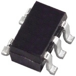
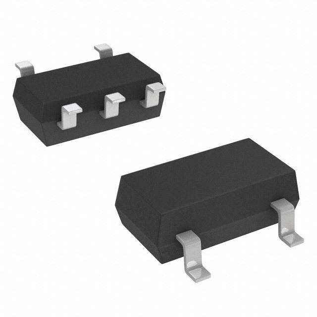
| 产品图片 |
|
| rohs | 符合RoHS无铅 / 符合限制有害物质指令(RoHS)规范要求 |
| 产品系列 | 放大器 IC,精密放大器,Analog Devices AD8515ARTZ-R2- |
| 数据手册 | |
| 产品型号 | AD8515ARTZ-R2 |
| 产品培训模块 | http://www.digikey.cn/PTM/IndividualPTM.page?site=cn&lang=zhs&ptm=30008http://www.digikey.cn/PTM/IndividualPTM.page?site=cn&lang=zhs&ptm=26202 |
| 产品种类 | 精密放大器 |
| 供应商器件封装 | SOT-23-5 |
| 共模抑制比—最小值 | 75 dB |
| 关闭 | No |
| 其它名称 | AD8515ARTZ-R2DKR |
| 包装 | Digi-Reel® |
| 压摆率 | 2.7 V/µs |
| 可用增益调整 | 112 dB |
| 商标 | Analog Devices |
| 增益带宽生成 | 5 MHz |
| 增益带宽积 | 5MHz |
| 安装类型 | 表面贴装 |
| 安装风格 | SMD/SMT |
| 封装 | Reel |
| 封装/外壳 | SC-74A,SOT-753 |
| 封装/箱体 | SOT-23-5 |
| 工作温度 | -40°C ~ 125°C |
| 工作电源电压 | 1.8 V to 5.5 V |
| 工厂包装数量 | 250 |
| 放大器类型 | 通用 |
| 最大工作温度 | + 125 C |
| 最小工作温度 | - 40 C |
| 标准包装 | 1 |
| 电压-电源,单/双 (±) | 1.8 V ~ 5 V |
| 电压-输入失调 | 1mV |
| 电压增益dB | 126.02 dB |
| 电流-电源 | 410µA |
| 电流-输入偏置 | 5pA |
| 电流-输出/通道 | 20mA |
| 电源电压-最大 | 5 V |
| 电源电压-最小 | 1.8 V |
| 电源电流 | 410 uA |
| 电源类型 | Single |
| 电路数 | 1 |
| 系列 | AD8515 |
| 视频文件 | http://www.digikey.cn/classic/video.aspx?PlayerID=1364138032001&width=640&height=505&videoID=2245193153001 |
| 设计资源 | |
| 转换速度 | 2.7 V/us |
| 输入偏压电流—最大 | 600 pA |
| 输入电压范围—最大 | 5 V |
| 输入补偿电压 | 1 mV |
| 输出类型 | 满摆幅 |
| 通道数量 | 1 Channel |


- 商务部:美国ITC正式对集成电路等产品启动337调查
- 曝三星4nm工艺存在良率问题 高通将骁龙8 Gen1或转产台积电
- 太阳诱电将投资9.5亿元在常州建新厂生产MLCC 预计2023年完工
- 英特尔发布欧洲新工厂建设计划 深化IDM 2.0 战略
- 台积电先进制程称霸业界 有大客户加持明年业绩稳了
- 达到5530亿美元!SIA预计今年全球半导体销售额将创下新高
- 英特尔拟将自动驾驶子公司Mobileye上市 估值或超500亿美元
- 三星加码芯片和SET,合并消费电子和移动部门,撤换高东真等 CEO
- 三星电子宣布重大人事变动 还合并消费电子和移动部门
- 海关总署:前11个月进口集成电路产品价值2.52万亿元 增长14.8%


PDF Datasheet 数据手册内容提取
1.8 V Low Power CMOS Rail-to-Rail Input/Output Operational Amplifier Data Sheet AD8515 FEATURES PIN CONFIGURATION Single-supply operation: 1.8 V to 5 V OUT 1 5 V+ Offset voltage: 6 mV maximum AD8515 Space-saving SOT-23 and SC70 packages V– 2 TOP VIEW SBRlaaeinwl-dt rwoa-itrdeat:ih l2 :i. n75p VMu/tHμ asz n d output swing +IN 3 (Not to Scale) 4 –IN 03024-001 Figure 1. 5-Lead SC70 and 5-Lead SOT-23 Low input bias current: 2 pA typical (KS and RJ Suffixes) Low supply current @ 1.8 V: 450 μA maximum APPLICATIONS Portable communications Portable phones Sensor interfaces Laser scanners PCMCIA cards Battery-powered devices New generation phones Personal digital assistants GENERAL DESCRIPTION The AD8515 is a rail-to-rail amplifier that can operate from The AD8515 is a rail-to-rail input and output amplifier with a single-supply voltage as low as 1.8 V. a gain bandwidth of 5 MHz and typical offset voltage of 1 mV from a 1.8 V supply. The low supply current makes these parts The AD8515 single amplifier, available in 5-lead SOT-23 and 5-lead ideal for battery-powered applications. The 2.7 V/μs slew rate SC70 packages, is small enough to be placed next to sensors, makes the AD8515 a good match for driving ASIC inputs such reducing external noise pickup. as voice codecs. The AD8515 is specified over the extended industrial temperature range of −40°C to +125°C. Rev. E Document Feedback Information furnished by Analog Devices is believed to be accurate and reliable. However, no responsibility is assumed by Analog Devices for its use, nor for any infringements of patents or other One Technology Way, P.O. Box 9106, Norwood, MA 02062-9106, U.S.A. rights of third parties that may result from its use. Specifications subject to change without notice. No license is granted by implication or otherwise under any patent or patent rights of Analog Devices. Tel: 781.329.4700 ©2002–2017 Analog Devices, Inc. All rights reserved. Trademarks and registered trademarks are the property of their respective owners. Technical Support www.analog.com
AD8515 Data Sheet TABLE OF CONTENTS Features .............................................................................................. 1 Typical Performance Characteristics ..............................................7 Applications ....................................................................................... 1 Theory of Operation ...................................................................... 12 Pin Configuration ............................................................................. 1 Power Consumption vs. Bandwidth ........................................ 12 General Description ......................................................................... 1 Driving Capacitive Loads .............................................................. 13 Revision History ............................................................................... 2 Full Power Bandwidth ............................................................... 13 Specifications ..................................................................................... 3 A Micropower Reference Voltage Generator .............................. 14 Electrical Characteristics ............................................................. 3 A 100 kHz Single-Supply Second-Order Band-Pass Filter ... 14 Absolute Maximum Ratings ............................................................ 6 Wien Bridge Oscillator .............................................................. 15 Thermal Resistance ...................................................................... 6 Outline Dimensions ....................................................................... 16 ESD Caution .................................................................................. 6 Ordering Guide .......................................................................... 16 REVISION HISTORY 1/2017—Rev. D to Rev. E 2/2003—Rev. 0 to Rev. A Changes to Ordering Guide .......................................................... 16 Added new SC70 Package ................................................. Universal Changes to Features .......................................................................... 1 7/2007—Rev. C to Rev. D Changes to General Description ..................................................... 1 Changes to Ordering Guide .......................................................... 16 Changes to Pin Configuration ......................................................... 1 Updated Package Designator Throughout .................................... 1 Changes to Specifications ................................................................. 2 Changes to Table 1, Supply Current/Amplifier ............................ 3 Changes to Absolute Maximum Ratings ........................................ 5 7/2007—Rev. C to Rev. D Changes to Ordering Guide ............................................................. 5 Changes to TPC 3 .............................................................................. 6 Updated Format .................................................................. Universal Changes to TPC 10 ............................................................................ 7 Updated Package Designator Throughout .................................... 1 Changes to TPC 13 ............................................................................ 8 Changes to Table 1, Supply Current/Amplifier ............................ 3 Changes to TPC 27 ......................................................................... 10 Changes to Table 2, Supply Current/Amplifier ............................ 4 Changes to TPC 28 ......................................................................... 10 Changes to Table 3, Large Signal Voltage Gain, Power Supply Added new TPC 29 ........................................................................ 10 Rejection Ratio, and Supply Current/Amplifier ........................... 5 Changes to Functional Description .............................................. 11 Changes to Figure 10 ........................................................................ 8 Updated to Outline Dimensions .................................................. 14 Changes to Figure 35 ...................................................................... 14 Updated Outline Dimensions ....................................................... 16 8/2002—Revision. 0: Initial Version Changes to Ordering Guide .......................................................... 16 3/2005—Rev. B to Rev. C Changes to Specifications ................................................................ 2 Changes to Ordering Guide ............................................................ 5 4/2003—Rev. A to Rev. B Change to Figure 5 ......................................................................... 12 Rev. E | Page 2 of 16
Data Sheet AD8515 SPECIFICATIONS ELECTRICAL CHARACTERISTICS V = 1.8 V, V = V/2, T = 25°C, unless otherwise noted. S CM S A Table 1. Parameter Symbol Conditions Min Typ Max Unit INPUT CHARACTERISTICS Offset Voltage V V = V/2 1 6 mV OS CM S −40°C < T < +125°C 8 mV A Input Bias Current I V = 1.8 V 2 30 pA B S −40°C < T < +85°C 600 pA A −40°C < T < +125°C 8 nA A Input Offset Current I 1 10 pA OS −40°C < T < +125°C 500 pA A Input Voltage Range 0 1.8 V Common-Mode Rejection Ratio CMRR 0 V ≤ V ≤ 1.8 V 50 dB CM −40°C < T < +125°C 47 dB A Large Signal Voltage Gain A R = 100 kΩ, 0.3 V ≤ V ≤ 1.5 V 110 400 V/mV VO L OUT Offset Voltage Drift ΔV /ΔT 4 μV/°C OS OUTPUT CHARACTERISTICS Output Voltage High V I = 100 µA, −40°C < T < +125°C 1.79 V OH L A I = 750 µA, −40°C < T < +125°C 1.77 V L A Output Voltage Low V I = 100 µA, −40°C < T < +125°C 10 mV OL L A I = 750 µA, −40°C < T < +125°C 30 mV L A Short-Circuit Limit I 20 mA SC POWER SUPPLY Supply Current/Amplifier I V = V/2 325 450 µA SY OUT S –40°C < T < +125°C 500 μA A DYNAMIC PERFORMANCE Slew Rate SR R = 10 kΩ 2.7 V/μs L Gain Bandwidth Product GBP 5 MHz NOISE PERFORMANCE Voltage Noise Density e f = 1 kHz 22 nV/√Hz n f = 10 kHz 20 nV/√Hz Current Noise Density i f = 1 kHz 0.05 pA/√Hz n Rev. E | Page 3 of 16
AD8515 Data Sheet V = 3.0 V, V = V/2, T = 25°C, unless otherwise noted. S CM S A Table 2. Parameter Symbol Conditions Min Typ Max Unit INPUT CHARACTERISTICS Offset Voltage V V = V/2 1 6 mV OS CM S −40°C < T < +125°C 8 mV A Input Bias Current I V = 3.0 V 2 30 pA B S −40°C < T < +85°C 600 pA A −40°C < T < +125°C 8 nA A Input Offset Current I 1 10 pA OS −40°C < T < +125°C 500 pA A Input Voltage Range 0 3 V Common-Mode Rejection Ratio CMRR 0 V ≤ V ≤ 3.0 V 54 dB CM −40°C < T < +125°C 50 dB A Large Signal Voltage Gain A R = 100 kΩ, 0.3 V ≤ V ≤ 2.7 V 250 1000 V/mV VO L OUT Offset Voltage Drift ΔV /ΔT 4 μV/°C OS OUTPUT CHARACTERISTICS Output Voltage High V I = 100 μA, −40°C < T < +125°C 2.99 V OH L A I = 750 μA, −40°C < T < +125°C 2.98 V L A Output Voltage Low V I = 100 μA, −40°C < T < +125°C 10 mV OL L A I = 750 μA, −40°C < T < +125°C 20 mV L A POWER SUPPLY Power Supply Rejection Ratio PSRR V = 1.8 V to 5.0 V 65 85 dB S −40°C < T < +125°C 57 80 dB A Supply Current/Amplifier I V = V/2 350 450 μA SY OUT S −40°C < T < +125°C 500 μA A DYNAMIC PERFORMANCE Slew Rate SR R = 10 kΩ 2.7 V/µs L Gain Bandwidth Product GBP 5 MHz NOISE PERFORMANCE Voltage Noise Density e f = 1 kHz 22 nV/√Hz n f = 10 kHz 20 nV/√Hz Current Noise Density i f = 1 kHz 0.05 pA/√Hz n Rev. E | Page 4 of 16
Data Sheet AD8515 V = 5.0 V, V = V/2, T = 25°C, unless otherwise noted. S CM S A Table 3. Parameter Symbol Conditions Min Typ Max Unit INPUT CHARACTERISTICS Offset Voltage V V = V/2 1 6 mV OS CM S –40°C < T < +125°C 8 mV A Input Bias Current I V = 5.0 V 5 30 pA B S –40°C < T < +85°C 600 pA A –40°C < T < +125°C 8 nA A Input Offset Current I 1 10 pA OS –40°C < T < +125°C 500 pA A Input Voltage Range 0 5.0 V Common-Mode Rejection Ratio CMRR 0 V ≤ V ≤ 5.0 V 60 75 dB CM –40°C < T < +125°C 54 dB A Large Signal Voltage Gain A R = 100 kΩ, 0.3 V ≤ V ≤ 4.7 V 450 2000 V/mV VO L OUT Offset Voltage Drift ΔV /ΔT 4 μV/°C OS OUTPUT CHARACTERISTICS 4.99 Output Voltage High V I = 100 μA, –40°C < T < +125°C 4.98 V OH L A I = 750 μA, –40°C < T < +125°C V L A Output Voltage Low V I = 100 μA, –40°C < T < +125°C 10 mV OL L A I = 750 μA, –40°C < T < +125°C 20 mV L A POWER SUPPLY Power Supply Rejection Ratio PSRR V = 1.8 V to 5.0 V 65 85 dB S –40°C < T < +125°C 57 80 dB A Supply Current/Amplifier I V = V/2 410 550 μA SY OUT S –40°C < T < +125°C 600 μA A DYNAMIC PERFORMANCE Slew Rate SR R = 10 kΩ 2.7 V/μs L Gain Bandwidth Product GBP 5 MHz NOISE PERFORMANCE Voltage Noise Density e f = 1 kHz 22 nV/√Hz n f = 10 kHz 20 nV/√Hz Current Noise Density i f = 1 kHz 0.05 pA/√Hz n Rev. E | Page 5 of 16
AD8515 Data Sheet ABSOLUTE MAXIMUM RATINGS T = 25°C, unless otherwise noted. A THERMAL RESISTANCE Table 4. Parameter Rating θ is specified for the worst-case conditions, that is, a device JA Supply Voltage 6 V soldered in a circuit board for surface-mount packages. Input Voltage GND to V S Differential Input Voltage ±6 V or ±V Table 5. Thermal Resistance S Output Short-Circuit Duration to GND Observe derating curves Package Type θJA θJC Unit Storage Temperature Range 5-Lead SOT-23 (RJ) 230 146 °C/W KS and RJ Packages −65°C to +150°C 5-Lead SC70 (KS) 376 126 °C/W Operating Temperature Range AD8515 −40°C to +125°C ESD CAUTION Junction Temperature Range KS and RJ Packages −65°C to +150°C Lead Temperature (Soldering, 60 sec) 300°C Stresses at or above those listed under Absolute Maximum Ratings may cause permanent damage to the product. This is a stress rating only; functional operation of the product at these or any other conditions above those indicated in the operational section of this specification is not implied. Operation beyond the maximum operating conditions for extended periods may affect product reliability. Rev. E | Page 6 of 16
Data Sheet AD8515 TYPICAL PERFORMANCE CHARACTERISTICS 450 6 VS = ±2.5V 5 400 SUPPLY CURRENT (µA) 330500 SUPPLY VOLTAGE (V) 432 250 1 200 03024-002 0 03024-005 4.65 4.70 4.75 4.80 4.85 4.90 4.95 4.65 4.70 4.75 4.80 4.85 4.90 4.95 BANDWIDTH (MHz) BANDWIDTH (MHz) Figure 2. Supply Current vs. Bandwidth Figure 5. Supply Voltage vs. Bandwidth 450 160 VS = ±2.5V 400 140 VOL 350 SUPPLY CURRENT (µA) 322110505000000 ΔOUTPUT VOLTAGE (mV) 112086400000 VOH 500 03024-003 200 03024-006 0 1 2 3 4 5 6 0 5 10 15 20 SUPPLY VOLTAGE (V) LOAD CURRENT (mA) Figure 3. Supply Current vs. Supply Voltage Figure 6. Output Voltage to Supply Rail vs. Load Current 500 120 270 VS = 5V VS = ±2.5V 100 AMPLITUDE = 20mV 225 80 180 450 GAIN 60 135 S) E A) dB) 40 PHASE 90 GRE I (µSY 400 GAIN ( 200 405 ASE (DE H P –20 –45 350 –40 –90 300 03024-004 ––6800 ––113850 03024-007 –50 –25 0 25 50 75 100 125 150 1k 10k 100k 1M 10M 50M TEMPERATURE (°C) FREQUENCY (Hz) Figure 4. ISY vs. Temperature Figure 7. Gain and Phase vs. Frequency Rev. E | Page 7 of 16
AD8515 Data Sheet 120 96 VS = ±2.5V VS = ±2.5V 100 80 92 60 G = 100 A (dB)CL 4200 GG == 110 SRR (dB) 88 0 P 84 –20 –40 80 ––6800 03024-008 76 03024-011 10k 100k 1M 10M 30M –50 0 50 100 150 FREQUENCY (Hz) TEMPERATURE (°C) Figure 8. ACL vs. Frequency Figure 11. PSRR vs. Temperature 120 430 VS = ±2.5V VS = ±2.5V 100 AMPLITUDE = 50mV 80 344 S R 60 E FI B) 40 PLI 258 d M CMRR ( 200 ER OF A 172 B M –20 U N –40 86 ––6800 03024-009 0 03024-012 10k 100k 1M 10M 100M –6.24 –4.27 –2.29 –0.32 1.66 3.63 FREQUENCY (Hz) VOS (mV) Figure 9. CMRR vs. Frequency Figure 12. VOS Distribution 140 150 VS = ±2.5V VS = ±2.5V AMPLITUDE = 50mV 120 100 +PSRR Ω) CE ( 100 B) 80 AN d D RR ( 60 –PSRR MPE PS T I 40 PU T 50 U O 20 –200 03024-010 0 GAIN = 100 GAIN = 10 GAIN = 1 03024-013 100 1k 10k 100k 1M 1k 10k 100k 1M 10M FREQUENCY (Hz) FREQUENCY (Hz) Figure 10. PSRR vs. Frequency Figure 13. Output Impedance vs. Frequency Rev. E | Page 8 of 16
Data Sheet AD8515 25 VS = 5V VS = ±2.5V 24 VIN = 6.4V 23 22 V) VIN 21 –ISC V/DI VOUT mA) E (2 I (SC 2109 +ISC OLTAG V 18 17 1165 03024-014 03024-017 –50 0 50 100 150 TEMPERATURE (°C) TIME (200µs/DIV) Figure 14. ISC vs. Temperature Figure 17. No Phase Reversal VS = ±2.5V VS = ±2.5V CL = 50pF VIN = 200mV VOLTAGE (13µV/DIV) VOLTAGE (100mV/DIV) 03024-015 03024-018 0 250 500 750 1k 1.25k 1.5k 1.75k 2k 2.25k 2.5k FREQUENCY (Hz) TIME (1µs/DIV) Figure 15. Voltage Noise Density Figure 18. Small Signal Transient Response VGSA I=N ± =2 .150V0 VCSL == ±520.05pVF VIN = 200mV V) V) DI DI V/ V/ m m 0 0 0 0 2 1 E ( E ( G G A A T T L L O O V V 03024-016 03024-019 TIME (1s/DIV) TIME (1µs/DIV) Figure 16. Input Voltage Noise Figure 19. Small Signal Transient Response Rev. E | Page 9 of 16
AD8515 Data Sheet 120 VS = ±2.5V VS = ±1.5V CL = 300pF 100 AMPLITUDE = 50mV VIN = 4V 80 V) 60 DI TAGE (1V/ MRR (dB) 4200 OL C 0 V –20 –40 03024-020 ––6800 03024-023 10k 100k 1M 10M 100M TIME (1µs/DIV) FREQUENCY (Hz) Figure 20. Large Signal Transient Response Figure 23. CMRR vs. Frequency 100mV VIN VGSA I=N ± =1 .–54V0 VCSL == ±500.p9FV VIN = 100mV VIN = 200mV V) DI 0V V/ E m G 0 VOLTA 0V AGE (10 T L 2V O V VOUT 03024-021 03024-024 TIME (2µs/DIV) TIME (1µs/DIV) Figure 21. Saturation Recovery Figure 24. Small Signal Transient Response 120 270 0V VGSA I=N ± =1 .–54V0 VIN 100 VASM =P L±I0T.U9VDE = 20mV 225 VIN = 100mV 80 180 60 135 S) –100mV E GE B) 40 90 RE A d G LT 2V N ( 20 45 DE VO VOUT GAI 0 0 ASE ( H 0V P –20 –45 –40 –90 03024-022 ––8600 ––118305 03024-025 10k 100k 1M 10M 30M TIME (2µs/DIV) FREQUENCY (Hz) Figure 22. Saturation Recovery Figure 25. Gain and Phase vs. Frequency Rev. E | Page 10 of 16
Data Sheet AD8515 200 4.995 VS = ±0.9V VS = 5V IL = 750µA 4.994 Ω) 150 E ( C DAN V)4.993 PE 100 (H M O UT I V4.992 P T U O 50 4.991 GAIN = 100 0 GAIN = 10 GAIN = 1 03024-026 4.990 03024-029 1k 10k 100k 1M 10M –50 0 50 100 150 FREQUENCY (Hz) TEMPERATURE (°C) Figure 26. Output Impedance vs. Frequency Figure 29. VOH vs. Temperature 80 VS = ±0.9V VS = 5V VIN = 3.2V 77 VIN V) DI OLTAGE (1V/ VOUT CMRR (dB) 7741 V 68 03024-027 65 03024-030 –50 0 50 100 150 TIME (200µs/DIV) TEMPERATURE (°C) Figure 27. No Phase Reversal Figure 30. CMRR vs. Temperature 11 VS = 5V IL = 750µA 9 V) m (L 7 O V 5 3 03024-028 –50 0 50 100 150 TEMPERATURE (°C) Figure 28. VOL vs. Temperature Rev. E | Page 11 of 16
AD8515 Data Sheet THEORY OF OPERATION The AD8515, offered in space-saving SOT-23 and SC70 packages, This product solves the speed/power requirements for many is a rail-to-rail input and output operational amplifier that can applications. The wide bandwidth is also stable even when operated operate at supply voltages as low as 1.8 V. This product is fabri- with low supply voltages. Figure 5 shows the relationship between cated using 0.6 micron CMOS to achieve one of the best power the supply voltage vs. the bandwidth for the AD8515. consumption-to-speed ratios (that is, bandwidth) in the industry. The AD8515 is ideal for battery-powered instrumentation and With a small amount of supply current (less than 400 μA), handheld devices because it can operate at the end of discharge a wide unity gain bandwidth of 4.5 MHz is available for signal voltage of most popular batteries. Table 6 lists the nominal and processing. end of discharge voltages of several typical batteries. The input stage consists of two parallel, complementary, differ- Table 6. Typical Battery Life Voltage Range ential pairs of PMOS and NMOS. The AD8515 exhibits no Nominal End of Discharge phase reversal because the input signal exceeds the supply by Battery Voltage (V) Voltage (V) more than 0.6 V. Currents into the input pin must be limited Lead-Acid 2 1.8 to 5 mA or less by the use of external series resistance(s). The Lithium 2.6 to 3.6 1.7 to 2.4 AD8515 has a very robust ESD design and can stand ESD NiMH 1.2 1 voltages of up to 4000 V. NiCd 1.2 1 POWER CONSUMPTION vs. BANDWIDTH Carbon-Zinc 1.5 1.1 One of the strongest features of the AD8515 is the bandwidth stability over the specified temperature range while consuming small amounts of current. This effect is shown in Figure 2 through Figure 4. Rev. E | Page 12 of 16
Data Sheet AD8515 DRIVING CAPACITIVE LOADS Most amplifiers have difficulty driving large capacitive loads. VS = ±0.9V CL = 800pF Additionally, higher capacitance at the output can increase the GAIN = –1 amount of overshoot and ringing in the amplifier’s step response V) and can even affect the stability of the device. This is due to the DI V/ degradation of phase margin caused by additional phase lag from 0m 0 1 the capacitive load. The value of capacitive load that an amplifier E ( G can drive before oscillation varies with gain, supply voltage, input A T L signal, temperature, and other parameters. Unity gain is the most VO challenging configuration for driving capacitive loads. The AD8515 icso cmappeanbslea toiof nd. rTivhien ggr laaprhgse icna pFiagcuitriev 3e 1l oaandds F wigiuthreo u3t2 asnhyo wex ttehren al 03024-033 amplifier’s capacitive load driving capability when configured TIME (1µs/DIV) in unity gain of +1. Figure 33. Capacitive Load Driving @ CL = 800 pF The AD8515 is even capable of driving higher capacitive loads FULL POWER BANDWIDTH in inverting gain of −1, as shown in Figure 33. The slew rate of an amplifier determines the maximum frequency VS = ±2.5V CL = 50pF at which it can respond to a large input signal. This frequency GAIN = 1 (known as full power bandwidth, FPBW) can be calculated from V) the equation DI 0mV/ FPBW = SR 10 2π×V E ( PEAK G TA for a given distortion. The FPBW of the AD8515 is shown in L O V Figure 34 to be close to 200 kHz. 03024-031 VIN TIME (1µs/DIV) V) DI Figure 31. Capacitive Load Driving @ CL = 50 pF V/ 2 E ( G A T L VS = ±2.5V VO CL = 500pF GAIN = 1 V/DIV) VOUT 03024-034 m 0 E (1 TIME (2µs/DIV) G A Figure 34. Full Power Bandwidth T L O V 03024-032 TIME (1µs/DIV) Figure 32. Capacitive Load Driving @ CL = 500 pF Rev. E | Page 13 of 16
AD8515 Data Sheet A MICROPOWER REFERENCE VOLTAGE GENERATOR 1 Many single-supply circuits are configured with the circuit f = L 2π×R1×C1 biased to one-half of the supply voltage. In these cases, a false ground reference can be created by using a voltage divider buffered 1 f = by an amplifier. Figure 35 shows the schematic for such a circuit. H 2π×R1×C1 The two 1 MΩ resistors generate the reference voltages while R1 drawing only 0.9 μA of current from a 1.8 V supply. A capacitor H =1+ 0 R2 connected from the inverting terminal to the output of the op amp provides compensation to allow for a bypass capacitor to be VCC=1.8V−5V connected at the reference output. This bypass capacitor helps where: establish an ac ground for the reference output. f is the low −3 dB frequency. L 1.8VTO 5V f is the high −3 dB frequency. H H is the midfrequency gain. 0 R2 C3 1RM1Ω 3 + V+ U11 10R04Ω 0.9VTO 2.5V VCC VCC 1µF 1MΩ 4 – V– AD8515 C1µ1F 1MRΩ6 2Rk5Ω 3 + U9 V11 V+ 1 VOUT 0.0C222µF 400mV 4 – V– AD8515 10Rk3Ω 03024-035 1CµF3 1MRΩ8 2Cn1F 5Rk1Ω R20 Figure 35. Micropower Voltage Reference Generator 20kΩ ABA 1N0D0 -kPHAzS SSI NFIGLTLEE-RS UPPLY SECOND-ORDER 0 1C0p6F 03024-036 Figure 36. Second-Order Band-Pass Filter The circuit in Figure 36 is commonly used in portable applica- tions where low power consumption and wide bandwidth are required. This figure shows a circuit for a single-supply band-pass 2 filter with a center frequency of 100 kHz. It is essential that the op amp have a loop gain at 100 kHz to maintain an accurate center 1.5 frequency. This loop gain requirement necessitates the choice of V) E ( an op amp with a high unity gain crossover frequency, such as G A the AD8515. The 4.5 MHz bandwidth of the AD8515 is sufficient LT VO 1 to accurately produce the 100 kHz center frequency, as the response T U in Figure 37 shows. When the op amp bandwidth is close to the TP U O center frequency of the filter, the amplifier internal phase shift 0.5 causes excess phase shift at 100 kHz, altering the filter response. Ithne f apchta, sife tshhei fcth oofs tehne oopp aammpp sh acas uas besa nthdew liodothp ctolo osesc tioll a1t0e0. kHz, 0 03024-037 1k 10k 100k 1M 10M 100M A common-mode bias level is easily created by connecting the FREQUENCY (Hz) noninverting input to a resistor divider consisting of two resistors Figure 37. Frequency Response of the Band-Pass Filter connected between VCC and ground. This bias point is also decoupled to ground with a 1 μF capacitor. Rev. E | Page 14 of 16
Data Sheet AD8515 WIEN BRIDGE OSCILLATOR High frequency oscillators can be built with the AD8515, due to its wide bandwidth. Using the values shown, an oscilla- The circuit in Figure 38 can be used to generate a sine wave, one tion frequency of 130 kHz is created and is shown in Figure 39. of the most fundamental waveforms. Known as a Wien Bridge If R11 is too low, the oscillation might converge; if too large, oscillator, it has the advantage of requiring only one low power the oscillation diverges until the output clips (V = ±2.5 V, amplifier. This is an important consideration, especially for battery- S f = 130 kHz). operated applications where power consumption is a critical issue. OSC To keep the equations simple, the resistor and capacitor values used are kept equal. For the oscillation to happen, two conditions have to be met. First, there should be a zero phase shift from the input to the output, which happens at the oscillation frequency of V) DI fOSC = 2πR101×C10 GE (2V/ A T L Second, at this frequency, the ratio of VOUT to the voltage at the VO positive input (+IN, Pin 3) has to be 3, which means that the ratio of R11:R12 should be greater than 2. 1Cn9F 1Rk1Ω9 03024-039 Figure 39. Output of Wien Bridge Oscillator VCC 3 + U10 V+ 1 C10 R13 2 – V– AD8515 1nF 1kΩ VEE R12 R11 1kΩ 2.05kΩ 03024-038 Figure 38. Low Power Wien Bridge Oscillator Rev. E | Page 15 of 16
AD8515 Data Sheet OUTLINE DIMENSIONS 3.00 2.90 2.80 1.70 5 4 3.00 1.60 2.80 1.50 2.60 1 2 3 0.95BSC 1.90 BSC 1.30 1.15 0.90 1.45MAX 0.20MAX 0.95MIN 0.08MIN 0.55 0.15MAX 10° 0.45 0.05MIN 0.50MAX SPELAATNIENG 5° B0S.6C0 0.35 0.35MIN 0° COMPLIANTTOJEDECSTANDARDSMO-178-AA 11-01-2010-A Figure 40. 5-Lead Small Outline Transistor Package [SOT-23] (RJ-5) Dimensions shown in millimeters 2.20 2.00 1.80 1.35 5 4 2.40 1.25 2.10 1.15 1 2 3 1.80 0.65BSC 1.00 1.10 0.40 0.90 0.80 0.10 0.70 0.46 0.10MAX 0.30 SPELAATNIENG 00..2028 0.36 COPLANARITY 0.15 0.26 0.10 COMPLIANTTOJEDECSTANDARDSMO-203-AA 072809-A Figure 41. 5-Lead Thin Shrink Small Outline Transistor Package [SC70] (KS-5) Dimensions shown in millimeters ORDERING GUIDE Model Temperature Range Package Description Package Option AD8515ARTZ-R21 −40°C to +125°C 5-Lead SOT-23 RJ-5 AD8515ARTZ-REEL1 −40°C to +125°C 5-Lead SOT-23 RJ-5 AD8515ARTZ-REEL71 −40°C to +125°C 5-Lead SOT-23 RJ-5 AD8515AKSZ-R21 −40°C to +125°C 5-Lead SC70 KS-5 AD8515AKSZ-REEL1 −40°C to +125°C 5-Lead SC70 KS-5 AD8515AKSZ-REEL71 −40°C to +125°C 5-Lead SC70 KS-5 1 Z = RoHS Compliant Part. ©2002–2017 Analog Devices, Inc. All rights reserved. Trademarks and registered trademarks are the property of their respective owners. D03024-0-1/17(E) Rev. E | Page 16 of 16