ICGOO在线商城 > 集成电路(IC) > 线性 - 放大器 - 仪表,运算放大器,缓冲器放大器 > AD626AR
 Datasheet下载
- 型号: AD626AR
- 制造商: Analog
- 库位|库存: xxxx|xxxx
- 要求:
| 数量阶梯 | 香港交货 | 国内含税 |
| +xxxx | $xxxx | ¥xxxx |
查看当月历史价格
查看今年历史价格
AD626AR产品简介:
ICGOO电子元器件商城为您提供AD626AR由Analog设计生产,在icgoo商城现货销售,并且可以通过原厂、代理商等渠道进行代购。 AD626AR价格参考¥69.16-¥78.59。AnalogAD626AR封装/规格:线性 - 放大器 - 仪表,运算放大器,缓冲器放大器, 差分 放大器 1 电路 8-SOIC。您可以下载AD626AR参考资料、Datasheet数据手册功能说明书,资料中有AD626AR 详细功能的应用电路图电压和使用方法及教程。
AD626AR 是 Analog Devices Inc.(亚德诺半导体公司)生产的一款低成本、低功耗的仪表放大器,广泛应用于需要高精度信号放大的场合。该器件具有高共模抑制比(CMRR)、宽工作温度范围和良好的稳定性,适合于工业控制、医疗设备和测试仪器等领域。

AD626AR 的主要应用场景包括:

1. 工业传感器接口:用于放大来自压力、温度、应变片等传感器的小信号,提高测量精度。
2. 医疗仪器:如心电图机(ECG)、血压监测仪等,用于放大微弱生物电信号。
3. 数据采集系统:在工业自动化中用于采集模拟信号并转换为数字信号进行处理。
4. 过程控制系统:用于工业控制中的信号调理,提高信号传输的稳定性和抗干扰能力。
5. 电池供电设备:由于其低功耗特性,适用于便携式或低功耗应用的仪器。

AD626AR 采用 8 引脚 SOIC 封装,易于集成,适合对成本和性能都有要求的应用场景。
| 参数 | 数值 |
| -3db带宽 | 100kHz |
| 产品目录 | 集成电路 (IC)半导体 |
| 描述 | IC OPAMP DIFF 100KHZ 8SOIC差分放大器 IC SINGLE SUPPLY |
| 产品分类 | Linear - Amplifiers - Instrumentation, OP Amps, Buffer Amps集成电路 - IC |
| 品牌 | Analog Devices Inc |
| 产品手册 | |
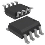
| 产品图片 |
|
| rohs | 否不符合限制有害物质指令(RoHS)规范要求 |
| 产品系列 | 放大器 IC,差分放大器,Analog Devices AD626AR- |
| 数据手册 | |
| 产品型号 | AD626AR |
| PCN组件/产地 | |
| 产品培训模块 | http://www.digikey.cn/PTM/IndividualPTM.page?site=cn&lang=zhs&ptm=25960http://www.digikey.cn/PTM/IndividualPTM.page?site=cn&lang=zhs&ptm=30008http://www.digikey.cn/PTM/IndividualPTM.page?site=cn&lang=zhs&ptm=26202 |
| 产品种类 | 差分放大器 |
| 供应商器件封装 | 8-SOIC |
| 共模抑制比—最小值 | 66 dB |
| 包装 | 管件 |
| 压摆率 | 0.22 V/µs |
| 商标 | Analog Devices |
| 增益带宽积 | - |
| 安装类型 | 表面贴装 |
| 安装风格 | SMD/SMT |
| 封装 | Tube |
| 封装/外壳 | 8-SOIC(0.154",3.90mm 宽) |
| 封装/箱体 | SOIC-8 |
| 工作温度 | -40°C ~ 85°C |
| 工作电源电压 | 5 V |
| 工厂包装数量 | 98 |
| 带宽 | 100 kHz |
| 放大器类型 | 差分 |
| 最大双重电源电压 | 6 V |
| 最大工作温度 | + 85 C |
| 最大输入电阻 | 200 kOhms |
| 最小工作温度 | - 40 C |
| 标准包装 | 98 |
| 电压-电源,单/双 (±) | 2.4 V ~ 12 V, ±1.2 V ~ 6 V |
| 电压-输入失调 | 50µV |
| 电流-电源 | 1.5mA |
| 电流-输入偏置 | - |
| 电流-输出/通道 | 12mA |
| 电源电流 | 0.23 mA, 1.5 mA |
| 电路数 | 1 |
| 稳定时间 | 24 us |
| 系列 | AD626 |
| 视频文件 | http://www.digikey.cn/classic/video.aspx?PlayerID=1364138032001&width=640&height=505&videoID=2245193153001http://www.digikey.cn/classic/video.aspx?PlayerID=1364138032001&width=640&height=505&videoID=2245193159001 |
| 转换速度 | 0.22 V/us |
| 输入补偿电压 | 1.9 mV, 50 uV |
| 输出类型 | - |
| 通道数量 | 1 Channel |


- 商务部:美国ITC正式对集成电路等产品启动337调查
- 曝三星4nm工艺存在良率问题 高通将骁龙8 Gen1或转产台积电
- 太阳诱电将投资9.5亿元在常州建新厂生产MLCC 预计2023年完工
- 英特尔发布欧洲新工厂建设计划 深化IDM 2.0 战略
- 台积电先进制程称霸业界 有大客户加持明年业绩稳了
- 达到5530亿美元!SIA预计今年全球半导体销售额将创下新高
- 英特尔拟将自动驾驶子公司Mobileye上市 估值或超500亿美元
- 三星加码芯片和SET,合并消费电子和移动部门,撤换高东真等 CEO
- 三星电子宣布重大人事变动 还合并消费电子和移动部门
- 海关总署:前11个月进口集成电路产品价值2.52万亿元 增长14.8%


PDF Datasheet 数据手册内容提取
Low Cost, Single-Supply Differential Amplifi er AD626 FEATURES CONNECTION DIAGRAM Pin Selectable Gains of 10 and 100 8-Lead Plastic Mini-DIP (N) True Single-Supply Operation and SOIC (R) Packages Single-Supply Range of +2.4 V to +10 V Dual-Supply Range of (cid:1)1.2 V to (cid:1)6 V Wide Output Voltage Range of 30 mV to 4.7 V 200k(cid:3) 200k(cid:3) –IN 1 8 +IN Optional Low-Pass Filtering 1/6 Excellent DC Performance ANALOG Low Input Offset Voltage: 500 (cid:2)V Max GND 2 G = 30 7 G = 100 Large Common-Mode Range: 0 V to +54 V –VS 3 6 +VS Low Power: 1.2 mW (V = +5 V) S 100k(cid:3) Good CMR of 90 dB Typ FILTER 4 G=2 5 OUT AC Performance AD626 Fast Settling Time: 24 (cid:2)s (0.01%) Includes Input Protection Series Resistive Inputs (RIN = 200 k(cid:3)) range of this amplifi er is equal to 6 (+VS – 1 V) which pro vides a RFI Filters Included +24 V CMR while operating from a +5 V supp ly. Fur therm ore, Allows 50 V Continuous Overload the AD626 features a CMR of 90 dB typ. APPLICATIONS The amplifi er’s inputs are protected against continuous overload of Current Sensing up to 50 V, and RFI fi lters are included in the attenuator network. Interface for Pressure Transducers, Position Indicators, The output range is +0.03 V to +4.9 V using a +5 V supp ly. The Strain Gages, and Other Low Level Signal Sources amplifi er provides a preset gain of 10, but gains be tween 10 and 100 can be easily confi g ured with an external res is tor. Fur ther - PROD UCT DES CRIPT ION more, a gain of 100 is available by connecting the G = 100 pin to The AD626 is a low cost, true sin gle-supp ly dif fer en tial am pli fi er analog ground. The AD626 also offers low-pass fi lter capability by de signed for amp li fy ing and low-pass fi ltering small diff er en tial connecting a ca pac i tor between the fi lter pin and analog ground. voltages from sources having a large common-mode voltage. The AD626A and AD626B operate over the industrial tem per a ture The AD626 can operate from either a single supply of +2.4 V to range of –40°C to +85°C. The AD626 is available in two 8-lead +10 V, or dual supplies of ±1.2 V to ±6 V. The input common-mode packages: a plastic mini-DIP and SOIC. 140 25 B 120 V d – 20 – E ON 100 NG ECTI GVS = = 1 +05, V100 E RA15 (cid:1)VCM FOR SINGLE EJ 80 OD AND DUAL SUPPLIES MODE R 60 GVS = = 1 (cid:1)005V MON-M10 COMMON- 40 GVS = = 1 (cid:1)05V NPUT COM 5 (cid:1)VCM FOR DUAL 20 I SUPPLIES ONLY 0 0 0.1 1 10 100 1k 10k 100k 1M 1 2 3 4 5 FREQUENCY – Hz SUPPLY VOLTAGE – (cid:1)V Figure 1. Common-Mode Rejection vs. Frequency Figure 2. Input Common-Mode Range vs. Supply REV. D Information furnished by Analog Devices is be lieved to be accurate and reliable. However, no responsibility is assumed by Analog Devices for its use, nor for any infringements of patents or other rights of third parties that may result from its use. No license is granted by implication or other- One Technology Way, P.O. Box 9106, Norwood, MA 02062-9106, U.S.A. wise under any patent or patent rights of Analog Devices.T rademarks and Tel: 781/329-4700 www.analog.com registered trademarks are the property of their respective companies. Fax: 781/326-8703 © 2003 Analog Devices, Inc. All rights reserved.
AD626–SPECIFICATIONS SINGLE SUPPLY (@+V = +5 V and T = 25(cid:4)C, un less oth er wise noted.) S A Model AD626A AD626B Parameter Condition Min Typ Max Min Typ Max Unit GAIN Gain Accuracy Total Error Gain = 10 @ VOUT ≥ 100 mV dc 0.4 1.0 0.2 0.6 % Gain = 100 @ VOUT ≥ 100 mV dc 0.1 1.0 0.5 0.6 % Over Temperature, T = T to T G = 10 50 30 ppm/°C A MIN MAX G = 100 150 120 ppm/°C Gain Linearity Gain = 10 @ VOUT ≥ 100 mV dc 0.014 0.016 0.014 0.016 % Gain = 100 @ VOUT ≥ 100 mV dc 0.014 0.02 0.014 0.02 % OFFSET VOLTAGE Input Offset Voltage 1.9 2.5 1.9 2.5 mV vs. Temperature T to T , G = 10 or 100 2.9 2.9 mV MIN MAX vs. Temperature T to T , G = 10 or 100 6 6 µV/°C MIN MAX vs. Supply Voltage (PSR) +PSR 74 80 74 80 dB –PSR 64 66 64 66 dB COMMON-MODE REJECTION R = 10 k(cid:1) L +CMR Gain = 10, 100 f = 100 Hz, V = +24 V 66 90 80 90 dB CM ±CMR Gain = 10, 100 f = 10 kHz, V = +6 V 55 64 55 64 dB CM –CMR Gain = 10, 100* f = 100 Hz, V = –2 V 60 85 73 85 dB CM COMMON-MODE VOLTAGE RANGE +CMV Gain = 10 CMR > 85 dB +24 +24 V –CMV Gain = 10 CMR > 85 dB –2 –2 V INPUT Input Resistance Differential 200 200 k(cid:1) Common-Mode 100 100 k(cid:1) Input Voltage Range (Common-Mode) 6 (V – l) 6 (V – l) V S S OUTPUT Output Voltage Swing R = 10 k(cid:1) L Positive Gain = 10 4.7 4.90 4.7 4.90 V Gain = 100 4.7 4.90 4.7 4.90 V Negative Gain = 10 0.03 0.03 V Gain = 100 0.03 0.03 V Short Circuit Current +I 12 12 mA SC NOISE Voltage Noise RTI Gain = 10 f = 0.1 Hz–10 Hz 2 2 µV p-p Gain = 100 f = 0.1 Hz–10 Hz 2 2 µV p-p Gain = 10 f = 1 kHz 0.25 0.25 µV/(cid:1)Hz Gain = 100 f = 1 kHz 0.25 0.25 µV/(cid:1)Hz DYNAMIC RESPONSE –3 dB Bandwidth V = +1 V dc 100 100 kHz OUT Slew Rate, T to T Gain = 10 0.17 0.22 0.17 0.22 V/µs MIN MAX Gain = 100 0.1 0.17 0.1 0.17 V/µs Settling Time to 0.01%, 1 V Step 24 22 µs POWER SUPPLY Operating Range T = T to T 2.4 5 12 2.4 5 10 V A MIN MAX Quiescent Current Gain = 10 0.16 0.20 0.16 0.20 mA Gain = 100 0.23 0.29 0.23 0.29 mA TRANSISTOR COUNT Number of Transistors 46 46 *At temperatures above 25°C, –CMV degrades at the rate of 12 mV/°C; i.e., @ 25°C CMV = –2 V, @ 85°C CMV = –1.28 V. Specifi cations subject to change without notice. –2– REV. D
AD626 DUAL SUPPLY (@+V = (cid:1)5 V and T = 25(cid:4)C, un less oth er wise noted.) S A Model AD626A AD626B Parameter Condition Min Typ Max Min Typ Max Unit GAIN Gain Accuracy Total Error Gain = 10 R = 10 k(cid:1) 0.2 0.5 0.1 0.3 % L Gain = 100 0.25 1.0 0.15 0.6 % Over Temperature, T = T to T G = 10 50 30 ppm/°C A MIN MAX G = 100 100 80 ppm/°C Gain Linearity Gain = 10 0.045 0.055 0.045 0.055 % Gain = 100 0.01 0.015 0.01 0.015 % OFFSET VOLTAGE Input Offset Voltage 50 500 50 250 µV vs. Temperature T to T , G = 10 or 100 1.0 0.5 mV MIN MAX vs. Temperature T to T , G = 10 or 100 1.0 0.5 µV/°C MIN MAX vs. Supply Voltage (PSR) +PSR 74 80 74 80 dB –PSR 64 66 64 66 dB COMMON-MODE REJECTION R = 10 k(cid:1) L +CMR Gain = 10, 100 f = 100 Hz, V = +24 V 66 90 80 90 dB CM ±CMR Gain = 10, 100 f = 10 kHz, V = 6 V 55 60 55 60 dB CM COMMON-MODE VOLTAGE RANGE +CMV Gain = 10 CMR > 85 dB 26.5 26.5 V –CMV Gain = 10 CMR > 85 dB 32.5 32.5 V INPUT Input Resistance Differential 200 200 k(cid:1) Common-Mode 110 110 k(cid:1) Input Voltage Range (Common-Mode) 6 (V – l) 6 (V – l) V S S OUTPUT Output Voltage Swing R = 10 k(cid:1) L Positive Gain = 10, 100 4.7 4.90 4.7 4.90 V Negative Gain = 10 –1.65 –2.1 –1.65 –2.1 V Gain = 100 –1.45 –1.8 –1.45 –1.8 V Short Circuit Current +I 12 12 mA SC –I 0.5 0.5 mA SC NOISE Voltage Noise RTI Gain = 10 f = 0.1 Hz–10 Hz 2 2 µV p-p Gain = 100 f = 0.1 Hz–10 Hz 2 2 µV p-p Gain = 10 f = 1 kHz 0.25 0.25 µV/(cid:1)Hz Gain = 100 f = 1 kHz 0.25 0.25 µV/(cid:1)Hz DYNAMIC RESPONSE –3 dB Bandwidth V = +1 V dc 100 100 kHz OUT Slew Rate, T to T Gain = 10 0.17 0.22 0.17 0.22 V/µs MIN MAX Gain = 100 0.1 0.17 0.1 0.17 V/µs Settling Time to 0.01%, 1 V Step 24 22 µs POWER SUPPLY Operating Range T = T to T (cid:2)1.2 (cid:2)5 (cid:2)6 (cid:2)1.2 (cid:2)5 (cid:2)6 V A MIN MAX Quiescent Current Gain = 10 1.5 2 1.5 2 mA Gain = 100 1.5 2 1.5 2 mA TRANSISTOR COUNT Number of Transistors 46 46 Specifi cations subject to change without notice. REV. D –3–
AD626 ABSOLUTE MAXIMUM RATINGS1 NOTES Supply Voltage . . . . . . . . . . . . . . . . . . . . . . . . . . . . . . . . . +36V 1Stresses above those listed under Absolute Maxi mum Ratings may cause perm a nent Internal Power Dissipation2 damage to the device. This is a stress rating only; functional operation of the device at these or any other conditions above those indicated in the operational section of Peak Input Voltage . . . . . . . . . . . . . . . . . . . . . . . . . . . . . .+60 V this specifi cation is not implied. Exposure to abs o lute maximum rating cond it ions Maximum Reversed Supply Voltage Limit . . . . . . . . . . . . . –34 V for extended periods may affect device rel i abili ty. Output Short Circuit Duration . . . . . . . . . . . . . . . . . . Indefi nite 28-Lead Plastic Package: (cid:3)JA = 100°C/W; (cid:3)JC = 50°C/W. Storage Temperature Range (N, R) . . . . . . . . .–65°C to +125°C 8-Lead SOIC Package: (cid:3)JA = 155°C/W; (cid:3)JC = 40°C/W. Operating Temperature Range AD626A/AD626B . . . . . . . . . . . . . . . . . . . .–40°C to +85°C Lead Temperature Range (Soldering 60 sec) . . . . . . . . . +300°C ORDERING GUIDE Temperature Package Package Model Range Description Option AD626AN –40°C to +85°C Plastic DIP N-8 AD626AR –40°C to +85°C Small Outline IC R-8 AD626BN –40°C to +85°C Plastic DIP N-8 AD626AR-REEL –40°C to +85°C 13" Tape and Reel AD626AR-REEL7 –40°C to +85°C 7" Tape and Reel METALLIZATION PHOTOGRAPH Dimensions shown in inches and (mm). CAUTION ESD (electrostatic discharge) sensitive device. Electrostatic charges as high as 4000 V readily ac cu mu late on the human body and test equipment and can discharge without detection. Although the AD626 features proprietary ESD prot ec tion circuitry, permanent damage may occur on devices subjected to high energy electrostatic discharges. Therefore, proper ESD pre caut ions are rec om mende d to avoid per form ance degr a da tion or loss of functionality. –4– REV. D
Typical Performance Characteristics–AD626 25 6 V 5 GVSA I=N (cid:1) =5 1V0, 100 NGE – 20 GE – V 4 A A E R15 (cid:1)VCM FOR SINGLE OLT D AND DUAL SUPPLIES V 3 MO UT MON-10 OUTP 2 INPUT COM 5 S(cid:1)UVPCPML FIEOSR ODNULAYL POSITIVE 01 0 –1 1 2 3 4 5 10 100 1k 10k SUPPLY VOLTAGE – (cid:1)V LOAD RESISTANCE – (cid:3) TPC 1. Input Common-Mode Range vs. Supply TPC 4. Positive Output Voltage Swing vs. Resistive Load 5 –6 – V TA = 25(cid:4)C –5 E SWING 4 SDIUNAGLL SEU APNPDLY TAGE – V–4 G L OLTA 3 UT VO–3 GAIN = 10 V P UT UT–2 P 2 O VE OUT DOUNALYL SUPPLY GATIVE –1 GAIN = 100 TI 1 E OSI N 0 P 0 1 0 1 2 3 4 5 100 1k 10k 100k SUPPLY VOLTAGE – V LOAD RESISTANCE – (cid:3) TPC 2. Positive Output Voltage Swing vs. Supply Voltage TPC 5. Negative Output Voltage Swing vs. Resistive Load –5 30 V TA = 25(cid:4)C – NG –4 (cid:2)V TAGE SWI–3 DUAL SUPPLY OLTAGE – 20 T VOL ONLY SET V PU–2 FF T O E OU E IN 10 V G ATI–1 AN G H E C N 0 0 1 2 3 4 5 0 SUPPLY VOLTAGE – V 0 1 2 3 4 5 WARM-UP TIME – Minutes TPC 3. Negative Output Voltage Swing vs. Supply Voltage TPC 6. Change in Input Offset Voltage vs. Warm-Up Time REV. D –5–
AD626 100 1000 95 VS = (cid:1)5V dB DUAL SUPPLY – OSED-LOOP GAIN 100 GGAAIINN == 11000 SINGLE VSSU =P P+L5YV N-MODE REJECTION 889050 VS = (cid:1)5 CL 10 MO75 M VDSU A= L(cid:1) S5UVPPLY CO70 010 100 1k 10k 100k 1M 6520 22 24 26 28 30 FREQUENCY – Hz INPUT COMMON-MODE VOLTAGE – V TPC 7. Closed-Loop Gain vs. Frequency TPC 10. Common-Mode Rejection vs. Input Common- Mode Voltage for Dual-Supply Operation 140 100 B 120 B G = 10, 100 d d ON – 100 ON – 90 TI G = 10, 100 TI EC VS = +5 EC J 80 J E E ODE R 60 GVS = = 1 (cid:1)005 ODE R80 M M N- N- MO 40 MO M G = 10 M70 CO VS = (cid:1)5 CO 20 0 60 0.1 1 10 100 1k 10k 100k 1M 0 20 40 60 80 FREQUENCY – Hz INPUT SOURCE RESISTANCE MISMATCH – (cid:3) TPC 8. Common-Mode Rejection vs. Frequency TPC 11. Common-Mode Rejection vs. Input Source Resistance Mismatch 100 0.7 G = 10, 100 CURVE APPLIES TO dB95 0.6 AALNLD SGUAPINPSLY B VEOTWLTEAEGNE 1S0 AND 100 – % ON 90 R – 0.5 TI O C R E R TOTAL GAIN ERROR = ODE REJ8805 L GAIN E 00..43 G+ AAIDND AITCIOCUNRAAL CGYA (INFR EORMR OSRPEC TABLE) M A MMON-75 VS = +5 DITION 0.2 CO AD 70 0.1 65 0.0 –5 0 5 10 15 20 25 10 100 1k INPUT COMMON-MODE VOLTAGE – V SOURCE RESISTANCE MISMATCH – (cid:3) TPC 9. Common-Mode Rejection vs. Input Common- TPC 12. Additional Gain Error vs. Source Mode Voltage for Single-Supply Operation Resistance Mismatch –6– REV. D
AD626 0.16 A N m0.15 O – SI T VI REN G = 10 L DI R A CU0.14 TIC CENT R VER S E E P QUI0.13 (cid:2)V 2 0.12 1 2 3 4 5 5 SECONDS PER HORIZONTAL DIVISION SUPPLY VOLTAGE – V TPC 13. Quiescent Supply Current vs. Supply Voltage TPC 16. 0.1 Hz to 10 Hz RTI Voltage Noise. V = ±5 V, S for Single-Supply Operation Gain = 100 2.0 100 80 A m1.5 RENT – P GAIN 60 FOR VS = (cid:1)5V AND +5V R O CU1.0 LO T D- EN SE 40 C O ES CL QUI0.5 20 0 0 (cid:1)1 (cid:1)2 (cid:1)3 (cid:1)4 (cid:1)5 1 10 100 1k 10k 100k 1M SUPPLY VOLTAGE – V VALUE OF RESISTOR RG – (cid:3) TPC 14. Quiescent Supply Current vs. Supply Voltage TPC 17. Closed-Loop Gain vs. R G for Dual-Supply Operation 10 140 ALL CURVES FOR GAINS OF 10 OR 100 B120 d – Hz N (cid:2)NSD – V/ 1.0 GAIN = 10, 100 Y REJECTIO10800 S–PINSGRLRE AND DUAL GE PPL A U VOLT 0.1 WER S 60 S+PINSGRLRE VS = (cid:1)5V DUAL SUPPLY PO 40 DDUUAALL ++PPSSRRRR 0.01 20 1 10 100 1k 10k 100k 0.1 1 10 100 1k 10k 100k 1M FREQUENCY – Hz FREQUENCY – Hz TPC 15. Noise Voltage Spectral Density vs. Frequency TPC 18. Power Supply Rejection vs. Frequency REV. D –7–
AD626 100 100 90 90 10 10 0% 0% TPC 19. Large Signal Pulse Response. V = ±5 V, G = 10 TPC 22. Large Signal Pulse Response. V = +5 V, G = 100 S S 100 100 90 90 10 10 0% 0% TPC 20. Large Signal Pulse Response. V = ±5 V, G = 100 TPC 23. Settling Time. V = ±5 V, G = 10 S S 500mV 100 100 90 90 10 10 0% 0% TPC 21. Large Signal Pulse Response. V = +5 V, G = 10 TPC 24. Settling Time. V = ±5 V, G = 100 S S –8– REV. D
AD626 100 100 90 90 10 10 0% 0% TPC 25. Settling Time. V = +5 V, G = 10 TPC 26. Settling Time. V = +5 V, G = 100 S S Figure 4 shows the main elements of the AD626. The signal in puts ERROR at Pins 1 and 8 are fi rst applied to dual resistive at ten u a tors R1 OUT 10k(cid:3) 10k(cid:3) through R4 whose purpose is to reduce the peak comm on-mode 2k(cid:3) voltage at the input to the preamplifi er—a feed back stage based +VS on the very low drift op amp A1. This allows the dif feren tial INPUT 10k(cid:3) input voltage to be accurately amplifi ed in the pres ence of large 20V p–p common-mode volt ag es six times greater than that which can be 1k(cid:3) AD626 tol er ate d by the actual input to A1. As a re sult, the in put CMR ex tends to six times the quantity (V – 1 V). The over all common- S mode error is mini mized by precise laser-trimming of R3 and R4, –VS thus giving the AD626 a common-mode rej ec tion ra tio (CMRR) of at least 10,000:1 (80 dB). Figure 3. Settling Time Test Circuit To minimize the effect of spurious RF signals at the inputs due to rectifi cation at the input to A1, small fi lter capacitors C1 and C2 THEORY OF OPERATION are included. The AD626 is a differential amplifi er con sist ing of a precision bal anced attenuator, a very low drift preamplifi er (A1), and an The output of A1 is connected to the in put of A2 via a 100 k(cid:1) out put buffer amplifi er (A2). It has been designed so that small (R12) resistor to facilitate the low-pass fi ltering of the sign al of differential signals can be accurately am pli fi ed and fi ltered in the in ter est (see Low-Pass Filtering section). presence of large common- mode voltages (VCM), without the use The 200 k(cid:1) input impedance of the AD626 requires that the source of any other active components. re sis tance driving this amplifi er be low in val ue (<1 k(cid:1))—this is +VS FILTER C1 AD626 R1 5pF 200k(cid:3) R12 +IN 100k(cid:3) A1 –IN A2 OUT R2 C2 200k(cid:3) 5pF R17 41kR(cid:3)3 R414k(cid:3) 95k(cid:3) R15 R9 10k(cid:3) 10k(cid:3) R5 R11 R6 4.2k(cid:3) R7 R8 R10 R14 R13 10k(cid:3) 500(cid:3) 500(cid:3) 10k(cid:3) 10k(cid:3) 555(cid:3) 10k(cid:3) GND GAIN = 100 –VS Figure 4. Simplifi ed Schematic REV. D –9–
AD626 necessary to mini mize gain error. Also, any mis match be tween the +INPUT total source res is tance at each input will af fect gain acc u ra cy and common- mode rejection (CMR). For ex am ple: when operating at a gain of 10, an 80 (cid:1) mismatch in the source re sis tance between –INPUT 1 –IN 200k(cid:3) 200k(cid:3) +IN 8 the inputs will degrade CMR to 68 dB. 1/6 The output buffer, A2, operates at a gain of 2 or 20, thus setting 2 AGNNADLOG G = 100 7 the overall, precalibrated gain of the AD626 (with no ex tern al G = 30 com po nents) at 10 or 100. The gain is set by the feedback net work –VS 3 –VS +VS 6 +VS around amplifi er A2. 0.1(cid:2)F 100k(cid:3) 0.1(cid:2)F The output of amplifi er A2 relies on a 10 k(cid:1) resistor to –V for FILTER OUT S 4 G = 2 5 OUTPUT “pull-down.” For single-supply operation, (–V = “GND”), A2 S AD626 can drive a 10 k(cid:1) ground refe r enced load to at least +4.7 V. The min i mum, nominally “zero,” output voltage will be 30 mV. For dual-supply ope r a tion (±5 V), the positive output voltage swing Figure 6. AD626 Confi gured for a Gain of 100 will be the same as for a single supply. The negative swing will be +INPUT to –2.5 V, at G = 100, limited by the ratio: –V × R15+R14 –IN 200k(cid:3) 200k(cid:3) +IN S R13+R14+R15 –INPUT 1 8 The negative range can be extended to –3.3 V (G = 100) and –4 V ANALOG 1/6 RH (G = 10) by addi ng an external 10 k(cid:1) pull-down from the out put 2 GND G = 30 G = 100 7 RG to –V . This will add 0.5 mA to the AD626’s qui es cent curr ent, S bringing the total to 2 mA. –VS 3 –VS +VS 6 +VS 0.1(cid:2)F 100k(cid:3) 0.1(cid:2)F The AD626’s 100 kHz bandwidth at G = 10 and 100 (a 10 MHz FILTER OUT gain bandwidth) is much higher than can be obtained with low CF 4 G = 2 5 OUTPUT power op amps in discrete dif fer en tial amplifi er circuits. Fur ther - FILTER AD626 (OPTIONAL) more, the AD626 is stable driving capacitive loads up to 50 pF 1 (G10) or 200 pF (G100). Capacitive load drive can be increased CORNER FREQUENCY OF FILTER =2(cid:5)CF (100k(cid:3)) to 200 pF (G10) by connecting a 100 (cid:1) resistor in series with the RESISTOR VALUES FOR GAIN ADJUSTMENT AD626’s output and the load. GAIN RANGE RG((cid:3)) RH((cid:3)) ADJUSTING THE GAIN OF THE AD626 11 – 20 100k 4.99k The AD626 is easily confi gured for gains of 10 or 100. Figure 5 20 – 40 10k 802 shows that for a gain of 10, Pin 7 is simply left un con nect ed; simi- 40 – 80 1k 80 80 – 100 100 2 larly, for a gain of 100, Pin 7 is grounded, as shown in Fig ure 6. Gains between 10 and 100 are easily set by connecting a varia ble Figure 7. Recommended Circuit for Gain Adjustment resistance between Pin 7 and Analog GND, as shown in Fig ure 7. Because the on-chip resistors have an absolute tole r ance of ±20% SINGLE-POLE LOW-PASS FILTERING (although they are ratio matched to within 0.1%), at least a 20% A low-pass fi lter can be easily implemented by using the feat ures adjustment range must be provided. The values shown in the provided by the AD626. table in Figure 7 provide a good trade-off bet ween gain set range By simply connecting a capacitor between Pin 4 and ground, and resolution, for gains from 11 to 90. a single-pole low-pass fi lter is created, as shown in Figure 8. +INPUT +INPUT –IN 200k(cid:3) 200k(cid:3) +IN –INPUT 1 8 –IN 200k(cid:3) 200k(cid:3) +IN –INPUT 1 8 1/6 2 AGNNADLOG G = 30 G = 10 7 NCOONTNECTED 2 AGNNADLOG 1/6 G = 100 7 G = 30 –VS 3 –VS +VS 6 +VS 0.1(cid:2)F 100k(cid:3) 0.1(cid:2)F 3 –VS +VS 6 +10V FILTER OUT 100k(cid:3) 0.1(cid:2)F 4 G = 2 5 OUTPUT FILTER OUT AD626 4 G = 2 5 OUTPUT CF AD626 Figure 5. AD626 Confi gured for a Gain of 10 CORNER FREQUENCY OF FILTER = 1 2(cid:5)CF (100k(cid:3)) Figure 8. A One-Pole Low-Pass Filter Circuit Which Operates from a Single +10 V Supply –10– REV. D
AD626 CURRENT SENSOR INTERFACE BRIDGE APPLICATION A typical current sensing application, making use of the large Figure 10 shows the AD626 in a typical bridge application. Here, common-mode range of the AD626, is shown in Figure 9. The the AD626 is set to operate at a gain of 100, using dual-sup ply curr ent being measured is sensed across resistor R . The value of voltages and offering the option of low-pass fi ltering. S R should be less than 1 k(cid:1) and should be selected so that the S average differential voltage across this resistor is typically 100 mV. +VS To produce a full-scale output of +4 V, a gain of 40 is used adjust- able by ±20% to absorb the tolerance in the sense res is tor. Note 1 –IN 200k(cid:3) 200k(cid:3) +IN 8 that there is suffi cient headroom to allow at least a 10% over range 1/6 (to +4.4 V). ANALOG 2 GND G = 100 7 G = 30 CURRENT IN CSUERNRSEONRT RS –5V 3 –VS +VS 6 +5V –IN 200k(cid:3) 200k(cid:3) +IN 0.1(cid:2)F 100k(cid:3) 0.1(cid:2)F CURRENT OUT 1 8 FILTER OUT CF 4 G = 2 5 OUTPUT ANALOG 1/6 RH LOOPWTI-OPANSASL AD626 2 GND G = 30 G = 100 7 RG FILTER Figure 10. A Typical Bridge Application –VS 3 –VS +VS 6 +VS 0.1(cid:2)F 100k(cid:3) 0.1(cid:2)F FILTER OUT CF 4 G = 2 5 OUTPUT OPTIONAL LOW-PASS AD626 FILTER Figure 9. Current Sensor Interface REV. D –11–
AD626 OUTLINE DIMENSIONS 8-Lead Standard Small Outline Package [SOIC] Narrow Body (R-8) Dimensions shown in millimeters and (inches) D) 5.00 (0.1968) 3( 4.80 (0.1890) 0 1/ – 0 8 5 – 4.00 (0.1574) 6.20 (0.2440) 1 3.80 (0.1497) 1 4 5.80 (0.2284) 078 0 C 1.27B (0S.C0500) 1.75 (0.0688) 00..5205 ((00..00109969)) (cid:6)45(cid:4) 1.35 (0.0532) 0.25 (0.0098) 0.10 (0.0040) COPL0A.1N0ARITY SEPALTAINNGE 00..5313 ((00..00210310)) 00..2159 ((00..00009785)) 80(cid:4)(cid:4) 10..2471 ((00..00510600)) COMPLIANT TO JEDEC STANDARDS MS-012AA CONTROLLING DIMENSIONS ARE IN MILLIMETERS; INCH DIMENSIONS (IN PARENTHESES) ARE ROUNDED-OFF MILLIMETER EQUIVALENTS FOR REFERENCE ONLY AND ARE NOT APPROPRIATE FOR USE IN DESIGN 8-Lead Plastic Dual-In Line Package [PDIP] (N-8) Dimensions shown in inches and (millimeters) 0.375 (9.53) 0.365 (9.27) 0.355 (9.02) 8 5 0.295 (7.49) 0.285 (7.24) 1 4 0.275 (6.98) 0.325 (8.26) 0.310 (7.87) 0.100 (2.54) 0.300 (7.62) 0.150 (3.81) BSC 0.135 (3.43) 0.180 0(0.0.3185) 0.120 (3.05) (4.57) MIN MAX 0.015 (0.38) 0.150 (3.81) SEATING 0.010 (0.25) 0.130 (3.30) PLANE 0.008 (0.20) 0.110 (2.79) 0.060 (1.52) 0.022 (0.56) 0.050 (1.27) 0.018 (0.46) 0.045 (1.14) 0.014 (0.36) COMPLIANT TO JEDEC STANDARDS MO-095AA CONTROLLING DIMENSIONS ARE IN INCHES; MILLIMETER DIMENSIONS (IN PARENTHESES) ARE ROUNDED-OFF INCH EQUIVALENTS FOR REFERENCE ONLY AND ARE NOT APPROPRIATE FOR USE IN DESIGN A. S. U. Revision History N D I E Location Page T N 1/03—Data Sheet changed from REV. C to REV. D. RI P Renumbered Figures and TPCs . . . . . . . . . . . . . . . . . . . . . . . . . . . . . . . . . . . . . . . . . . . . . . . . . . . . . . . . . . . . . . . . . . . . . . .Universal Edits to Figure 1 . . . . . . . . . . . . . . . . . . . . . . . . . . . . . . . . . . . . . . . . . . . . . . . . . . . . . . . . . . . . . . . . . . . . . . . . . . . . . . . . . . . . . . . . . 1 Edits to SPECIFICATIONS, Output . . . . . . . . . . . . . . . . . . . . . . . . . . . . . . . . . . . . . . . . . . . . . . . . . . . . . . . . . . . . . . . . . . . . . . . . . 3 Edit to ORDERING GUIDE . . . . . . . . . . . . . . . . . . . . . . . . . . . . . . . . . . . . . . . . . . . . . . . . . . . . . . . . . . . . . . . . . . . . . . . . . . . . . . . 4 Update to standard CAUTION/ESD Warning note and diagram . . . . . . . . . . . . . . . . . . . . . . . . . . . . . . . . . . . . . . . . . . . . . . . . . . . . 4 Edits to TPC 8 . . . . . . . . . . . . . . . . . . . . . . . . . . . . . . . . . . . . . . . . . . . . . . . . . . . . . . . . . . . . . . . . . . . . . . . . . . . . . . . . . . . . . . . . . . 6 Updated OUTLINE DIMENSIONS . . . . . . . . . . . . . . . . . . . . . . . . . . . . . . . . . . . . . . . . . . . . . . . . . . . . . . . . . . . . . . . . . . . . . . . . 12 –12– REV. D