ICGOO在线商城 > 集成电路(IC) > 线性 - 放大器 - 仪表,运算放大器,缓冲器放大器 > AD8132ARMZ
 Datasheet下载
- 型号: AD8132ARMZ
- 制造商: Analog
- 库位|库存: xxxx|xxxx
- 要求:
| 数量阶梯 | 香港交货 | 国内含税 |
| +xxxx | $xxxx | ¥xxxx |
查看当月历史价格
查看今年历史价格
AD8132ARMZ产品简介:
ICGOO电子元器件商城为您提供AD8132ARMZ由Analog设计生产,在icgoo商城现货销售,并且可以通过原厂、代理商等渠道进行代购。 AD8132ARMZ价格参考¥7.46-¥9.32。AnalogAD8132ARMZ封装/规格:线性 - 放大器 - 仪表,运算放大器,缓冲器放大器, 差分 放大器 1 电路 差分 8-MSOP。您可以下载AD8132ARMZ参考资料、Datasheet数据手册功能说明书,资料中有AD8132ARMZ 详细功能的应用电路图电压和使用方法及教程。
AD8132ARMZ是由Analog Devices Inc.(亚德诺半导体公司)生产的一款高性能仪表放大器,广泛应用于需要高精度信号处理的场景。以下是其主要应用场景:

 1. 工业自动化与控制
   AD8132ARMZ在工业自动化系统中用于传感器信号调理,特别是压力、温度、位移等传感器的信号放大和处理。它能够将微弱的传感器输出信号进行精确放大,同时抑制共模噪声,确保信号的稳定性和准确性。这使得它非常适合用于工厂自动化、过程控制等领域。

 2. 医疗设备
   在医疗设备中,AD8132ARMZ常用于心电图(ECG)、脑电图(EEG)等生物电信号的采集和放大。由于这些信号非常微弱且容易受到干扰,AD8132ARMZ的高共模抑制比(CMRR)和低噪声特性使其成为理想选择,能够有效提高信号的质量,确保诊断的准确性。

 3. 音频处理
   AD8132ARMZ在音频设备中也有广泛应用,如麦克风前置放大器、音频混音器等。它能够提供高增益和低失真,确保音频信号的清晰度和保真度。此外,其低功耗特性也使得它适合便携式音频设备的设计。

 4. 通信系统
   在通信系统中,AD8132ARMZ可用于射频(RF)信号的接收和处理。它可以作为前端放大器,对微弱的射频信号进行放大,同时保持信号的完整性,减少噪声的影响。这对于无线通信、卫星通信等应用至关重要。

 5. 数据采集系统
   AD8132ARMZ在数据采集系统中用于将模拟信号转换为数字信号之前进行预处理。它能够将来自各种传感器的信号进行放大和滤波,确保后续ADC(模数转换器)能够获得高质量的输入信号,从而提高整个系统的测量精度。

 6. 汽车电子
   在汽车电子领域,AD8132ARMZ可用于车载传感器信号的处理,如轮胎压力监测系统(TPMS)、发动机管理系统等。它能够在恶劣的电磁环境中提供稳定的信号放大,确保车辆的安全性和性能。

总之,AD8132ARMZ凭借其高精度、低噪声、高共模抑制比等特性,适用于多种需要精确信号处理的应用场景,尤其在工业、医疗、通信等领域表现出色。
| 参数 | 数值 |
| -3db带宽 | 360MHz |
| 产品目录 | 集成电路 (IC)半导体 |
| 描述 | IC OPAMP DIFF 360MHZ 8MSOP差分放大器 IC Hi-Speed |
| DevelopmentKit | AD8132ARM-EBZ |
| 产品分类 | Linear - Amplifiers - Instrumentation, OP Amps, Buffer Amps集成电路 - IC |
| 品牌 | Analog Devices |
| 产品手册 | |
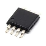
| 产品图片 |
|
| rohs | 符合RoHS无铅 / 符合限制有害物质指令(RoHS)规范要求 |
| 产品系列 | 放大器 IC,差分放大器,Analog Devices AD8132ARMZ- |
| 数据手册 | |
| 产品型号 | AD8132ARMZ |
| 产品培训模块 | http://www.digikey.cn/PTM/IndividualPTM.page?site=cn&lang=zhs&ptm=25960http://www.digikey.cn/PTM/IndividualPTM.page?site=cn&lang=zhs&ptm=30008http://www.digikey.cn/PTM/IndividualPTM.page?site=cn&lang=zhs&ptm=26202 |
| 产品目录页面 | |
| 产品种类 | 差分放大器 |
| 供应商器件封装 | 8-MSOP |
| 共模抑制比—最小值 | - 70 dB |
| 包装 | 管件 |
| 压摆率 | 1200 V/µs |
| 可用增益调整 | 1 V/V |
| 商标 | Analog Devices |
| 增益带宽积 | - |
| 安装类型 | 表面贴装 |
| 安装风格 | SMD/SMT |
| 封装 | Tube |
| 封装/外壳 | 8-TSSOP,8-MSOP(0.118",3.00mm 宽) |
| 封装/箱体 | MSOP-8 |
| 工作温度 | -40°C ~ 125°C |
| 工作电源电压 | 1.35 V to 5.5 V |
| 工厂包装数量 | 50 |
| 带宽 | 350 MHz |
| 放大器类型 | 差分 |
| 最大功率耗散 | 250 mW |
| 最大工作温度 | + 125 C |
| 最大输入电阻 | 3.5 MOhms |
| 最小工作温度 | - 40 C |
| 标准包装 | 50 |
| 电压-电源,单/双 (±) | 2.7 V ~ 11 V, ±1.35 V ~ 5.5 V |
| 电压-输入失调 | 1mV |
| 电流-电源 | 12mA |
| 电流-输入偏置 | 3µA |
| 电流-输出/通道 | 70mA |
| 电源电流 | 12 mA |
| 电路数 | 1 |
| 稳定时间 | 15 ns |
| 系列 | AD8132 |
| 视频文件 | http://www.digikey.cn/classic/video.aspx?PlayerID=1364138032001&width=640&height=505&videoID=2245193153001http://www.digikey.cn/classic/video.aspx?PlayerID=1364138032001&width=640&height=505&videoID=2245193159001 |
| 转换速度 | 1200 V/us |
| 输入补偿电压 | 1 mV |
| 输出电流 | 70 mA |
| 输出电流—典型值 | 70 mA |
| 输出类型 | 差分 |
| 通道数量 | 1 Channel |


- 商务部:美国ITC正式对集成电路等产品启动337调查
- 曝三星4nm工艺存在良率问题 高通将骁龙8 Gen1或转产台积电
- 太阳诱电将投资9.5亿元在常州建新厂生产MLCC 预计2023年完工
- 英特尔发布欧洲新工厂建设计划 深化IDM 2.0 战略
- 台积电先进制程称霸业界 有大客户加持明年业绩稳了
- 达到5530亿美元!SIA预计今年全球半导体销售额将创下新高
- 英特尔拟将自动驾驶子公司Mobileye上市 估值或超500亿美元
- 三星加码芯片和SET,合并消费电子和移动部门,撤换高东真等 CEO
- 三星电子宣布重大人事变动 还合并消费电子和移动部门
- 海关总署:前11个月进口集成电路产品价值2.52万亿元 增长14.8%


PDF Datasheet 数据手册内容提取
Low Cost, High Speed Differential Amplifier AD8132 FEATURES CONNECTION DIAGRAM High speed AD8132 350 MHz, −3 dB bandwidth –IN 1 8 +IN 1200 V/μs slew rate VOCM 2 7 NC V+ 3 6 V– Resistor set gain Internal common-mode feedback +OUT 4NC = NO CONNECT5 –OUT 01035-001 Improved gain and phase balance: −68 dB @ 10 MHz Figure 1. Separate input to set the common-mode output voltage Low distortion: −99 dBc SFDR @ 5 MHz, 800 Ω load The AD8132 is also used as a differential driver for the trans- Low power: 10.7 mA @ 5 V mission of high speed signals over low cost twisted pair or coaxial Power supply range: +2.7 V to ±5.5 V cables. The feedback network can be adjusted to boost the high Fully AEC-Q100 qualified (AD8132W) frequency components of the signal. The AD8132 is used for either analog or digital video signals or for other high speed data trans- APPLICATIONS mission. The AD8132 is capable of driving either a Category 3 or Category 5 twisted pair or coaxial cable with minimal line Low power differential ADC drivers attenuation. The AD8132 has considerable cost and performance Differential gain and differential filtering improvements over discrete line driver solutions. Video line drivers Differential in/out level shifting Differential signal processing reduces the effects of ground noise Single-ended input to differential output drivers that plagues ground-referenced systems. The AD8132 can be used Active transformers for differential signal processing (gain and filtering) throughout a Automotive driver assistance signal chain, easily simplifying the conversion between differential Automotive infotainment and single-ended components. GENERAL DESCRIPTION The AD8132W is the automotive grade version, qualified for 125°C operation per the AEC-Q100. See the Automotive The AD8132 is a low cost differential or single-ended input to Products section for more details. differential output amplifier with resistor set gain. The AD8132 is a major advancement over op amps for driving differential input The AD8132 is available in both 8-lead SOIC and 8-lead MSOP ADCs or for driving signals over long lines. The AD8132 has a packages for operation over the extended industrial temperature unique internal feedback feature that provides output gain and range of −40°C to +125°C. phase matching balanced to −68 dB at 10 MHz, suppressing 6 harmonics and reducing radiated EMI. VS = ±5V G = +1 Manufactured using the next-generation of Analog Devices, Inc., 3 RVOL,, ddmm == 429V9 pΩ-p XFCB bipolar process, the AD8132 has a −3 dB bandwidth of 0 350 MHz and delivers a differential signal with −99 dBc SFDR B) at 5 MHz, despite its low cost. The AD8132 eliminates the need for d N ( –3 a transformer with high performance ADCs, preserving the low AI G frequency and dc information. The common-mode level of the –6 differential output is adjustable by applying a voltage on the V pin, easily level shifting the input signals for driving single- OCM –9 supply ADCs. Fast overload recovery preserves sampling accuracy. –121 10FREQUENCY (MHz1)00 1k 01035-002 Figure 2. Large Signal Frequency Response Rev. I Information furnished by Analog Devices is believed to be accurate and reliable. However, no responsibility is assumed by Analog Devices for its use, nor for any infringements of patents or other One Technology Way, P.O. Box 9106, Norwood, MA 02062-9106, U.S.A. rights of third parties that may result from its use. Specifications subject to change without notice. No license is granted by implication or otherwise under any patent or patent rights of Analog Devices. Tel: 781.329.4700 www.analog.com Trademarks and registered trademarks are the property of their respective owners. Fax: 781.461.3113 ©2000–2009 Analog Devices, Inc. All rights reserved.
AD8132 TABLE OF CONTENTS Features .............................................................................................. 1 Differential Amplifier Without Resistors (High Input Applications ....................................................................................... 1 Impedance Inverting Amplifier) .............................................. 22 General Description ......................................................................... 1 Other β2 = 1 Circuits ................................................................. 23 Connection Diagram ....................................................................... 1 Varying β2 ................................................................................... 23 Revision History ........................................................................... 3 β1 = 0............................................................................................ 23 Specifications ..................................................................................... 4 Estimating the Output Noise Voltage ...................................... 23 ±D to ±OUT Specifications ...................................................... 4 Calculating Input Impedance of the Application Circuit ..... 24 IN V to ±OUT Specifications ..................................................... 5 Input Common-Mode Voltage Range in Single-Supply OCM Applications ................................................................................ 24 ±D to ±OUT Specifications ...................................................... 6 IN Setting the Output Common-Mode Voltage .......................... 24 V to ±OUT Specifications ..................................................... 7 OCM Driving a Capacitive Load ......................................................... 24 ±D to ±OUT Specifications ...................................................... 8 IN Open-Loop Gain and Phase ..................................................... 24 V to ±OUT Specifications ..................................................... 8 OCM Layout, Grounding, and Bypassing .............................................. 25 Absolute Maximum Ratings ............................................................ 9 Circuits ......................................................................................... 25 Thermal Resistance ...................................................................... 9 Applications Information .............................................................. 26 Maximum Power Dissipation ..................................................... 9 Analog-to-Digital Driver .......................................................... 26 ESD Caution .................................................................................. 9 Balanced Cable Driver ............................................................... 26 Pin Configuration and Function Descriptions ........................... 10 Transmit Equalizer ..................................................................... 27 Typical Performance Characteristics ........................................... 11 Low-Pass Differential Filter ...................................................... 27 Test Circuits ..................................................................................... 20 High Common-Mode Output Impedance Amplifier ........... 28 Operational Description ................................................................ 21 Full-Wave Rectifier .................................................................... 29 Definition of Terms .................................................................... 21 Automotive Products ................................................................. 29 Basic Circuit Operation ............................................................. 21 Outline Dimensions ....................................................................... 30 Theory of Operation ...................................................................... 22 Ordering Guide .......................................................................... 30 General Usage of the AD8132 .................................................. 22 Rev. I | Page 2 of 32
AD8132 REVISION HISTORY 9/09—Rev. H to Rev. I 11/05—Rev. D to Rev. E Changes to Figure 64 Caption ...................................................... 21 Changes to Table 7, Thermal Resistance Section, Maximum Power Dissipation Section, and Figure 3 ...................................... 8 5/09—Rev. G to Rev. H Changes to Ordering Guide .......................................................... 29 Changes to Features Section, Applications Section, and General Description Section .......................................................................... 1 12/04—Rev. C to Rev. D Changes to Table 1 ........................................................................... 4 Changes to General Description .................................................... 1 Changes to Table 2 ........................................................................... 5 Changes to Specifications ............................................................... 2 Changes to Table 3 ........................................................................... 6 Changes to Absolute Maximum Ratings....................................... 8 Changes to Table 4 ........................................................................... 7 Updated Outline Dimensions ....................................................... 29 Added Automotive Products Section .......................................... 29 Changes to Ordering Guide .......................................................... 29 Changes to Ordering Guide .......................................................... 30 2/03—Rev. B to Rev. C 1/09—Rev. F to Rev. G Changes to Specifications ............................................................... 2 Changes to Figure 77 ..................................................................... 26 Addition to Estimating the Output Noise Voltage Section ...... 15 Updated Outline Dimensions ....................................................... 29 Updated Outline Dimensions ....................................................... 21 11/06—Rev. E to Rev. F 1/02—Rev. A to Rev. B Updated Format ................................................................. Universal Edits to Transmitter Equalizer Section ....................................... 18 Changes to Table 1 ........................................................................... 3 Changes to Table 4 ........................................................................... 6 Changes to Table 5 ........................................................................... 7 Changes to Ordering Guide .......................................................... 29 Rev. I | Page 3 of 32
AD8132 SPECIFICATIONS ±D TO ±OUT SPECIFICATIONS IN At T = 25°C, V = ±5 V, V = 0 V, G = +1, R = 499 Ω, R = R = 348 Ω, unless otherwise noted. For G = +2, R = 200 Ω, R = 1000 Ω, A S OCM L, dm F G L, dm F R = 499 Ω. Refer to Figure 56 and Figure 57 for test setup and label descriptions. All specifications refer to single-ended input and G differential outputs, unless otherwise noted. Table 1. Parameter Conditions Min Typ Max Unit DYNAMIC PERFORMANCE −3 dB Large Signal Bandwidth V = 2 V p-p 300 350 MHz OUT AD8132W only, T to T 280 MHz MIN MAX V = 2 V p-p, G = +2 190 MHz OUT −3 dB Small Signal Bandwidth V = 0.2 V p-p 360 MHz OUT V = 0.2 V p-p, G = +2 160 MHz OUT Bandwidth for 0.1 dB Flatness V = 0.2 V p-p 90 MHz OUT V = 0.2 V p-p, G = +2 50 MHz OUT Slew Rate V = 2 V p-p 1000 1200 V/μs OUT AD8132W only, T to T 950 V/μs MIN MAX Settling Time 0.1%, V = 2 V p-p 15 ns OUT Overdrive Recovery Time V = 5 V to 0 V step, G = +2 5 ns IN NOISE/HARMONIC PERFORMANCE Second Harmonic V = 2 V p-p, 1 MHz, R = 800 Ω −96 dBc OUT L, dm V = 2 V p-p, 5 MHz, R = 800 Ω −83 dBc OUT L, dm V = 2 V p-p, 20 MHz, R = 800 Ω −73 dBc OUT L, dm Third Harmonic V = 2 V p-p, 1 MHz, R = 800 Ω −102 dBc OUT L, dm V = 2 V p-p, 5 MHz, R = 800 Ω −98 dBc OUT L, dm V = 2 V p-p, 20 MHz, R = 800 Ω −67 dBc OUT L, dm IMD 20 MHz, R = 800 Ω −76 dBc L, dm IP3 20 MHz, R = 800 Ω 40 dBm L, dm Input Voltage Noise (RTI) f = 0.1 MHz to 100 MHz 8 nV/√Hz Input Current Noise f = 0.1 MHz to 100 MHz 1.8 pA/√Hz Differential Gain Error NTSC, G = +2, R = 150 Ω 0.01 % L, dm Differential Phase Error NTSC, G = +2, R = 150 Ω 0.10 Degrees L, dm INPUT CHARACTERISTICS Offset Voltage (RTI) V = V /2; V = V = V = 0 V ±1.0 ±3.5 mV OS, dm OUT, dm DIN+ DIN− OCM AD8132W only, T to T ±6 mV MIN MAX T to T variation 10 μV/°C MIN MAX Input Bias Current T = 25°C 3 7 μA A AD8132W only, T to T 8 μA MIN MAX Input Resistance Differential 12 MΩ Common mode 3.5 MΩ Input Capacitance 1 pF Input Common-Mode Voltage −4.7 to +3.0 V CMRR ΔV /ΔV ; ΔV = ±1 V; resistors matched to 0.01% −70 −60 dB OUT, dm IN, cm IN, cm AD8132W only, T to T −60 dB MIN MAX OUTPUT CHARACTERISTICS Output Voltage Swing Maximum ΔV ; single-ended output −3.6 to +3.6 V OUT Output Current +70 mA Output Balance Error ΔV /ΔV ; ΔV = 1 V −70 dB OUT, cm OUT, dm OUT, dm Rev. I | Page 4 of 32
AD8132 V TO ±OUT SPECIFICATIONS OCM At T = 25°C, V = ±5 V, V = 0 V, G = +1, R = 499 Ω, R = R = 348 Ω, unless otherwise noted. For G = +2, R = 200 Ω, R = 1000 Ω, A S OCM L, dm F G L, dm F R = 499 Ω. Refer to Figure 56 and Figure 57 for test setup and label descriptions. All specifications refer to single-ended input and G differential outputs, unless otherwise noted. Table 2. Parameter Conditions Min Typ Max Unit DYNAMIC PERFORMANCE −3 dB Bandwidth ΔV = 600 mV p-p 210 MHz OCM Slew Rate ΔV = −1 V to +1 V 400 V/μs OCM Input Voltage Noise (RTI) f = 0.1 MHz to 100 MHz 12 nV/√Hz DC PERFORMANCE Input Voltage Range ±3.6 V Input Resistance 50 kΩ Input Offset Voltage V = V ; V = V = V = 0 V ±1.5 ±7 mV OS, cm OUT, cm DIN+ DIN− OCM AD8132W only, T to T ±9 mV MIN MAX Input Bias Current 0.5 μA V CMRR ΔV /ΔV ; ΔV = ±1 V; resistors matched to 0.01% −68 dB OCM OUT, dm OCM OCM Gain ΔV /ΔV ; ΔV = ±1 V 0.985 1 1.015 V/V OUT, cm OCM OCM AD8132W only, T to T 0.985 1.015 V/V MIN MAX POWER SUPPLY Operating Range ±1.35 ±5.5 V Quiescent Current V = V = V = 0 V 11 12 13 mA DIN+ DIN− OCM AD8132W only, T to T 9 14.5 mA MIN MAX T to T variation 16 μA/°C MIN MAX Power Supply Rejection Ratio ΔV /ΔV; ΔV = ±1 V −70 −60 dB OUT, dm S S AD8132W only, T to T −60 dB MIN MAX OPERATING TEMPERATURE RANGE −40 +125 °C Rev. I | Page 5 of 32
AD8132 ±D TO ±OUT SPECIFICATIONS IN At T = 25°C, V = 5 V, V = 2.5 V, G = +1, R = 499 Ω, R = R = 348 Ω, unless otherwise noted. For G = +2, R = 200 Ω, R = 1000 Ω, A S OCM L, dm F G L, dm F R = 499 Ω. Refer to Figure 56 and Figure 57 for test setup and label descriptions. All specifications refer to single-ended input and G differential outputs, unless otherwise noted. Table 3. Parameter Conditions Min Typ Max Unit DYNAMIC PERFORMANCE −3 dB Large Signal Bandwidth V = 2 V p-p 250 300 MHz OUT AD8132W only, T to T 240 MHz MIN MAX V = 2 V p-p, G = +2 180 MHz OUT −3 dB Small Signal Bandwidth V = 0.2 V p-p 360 MHz OUT V = 0.2 V p-p, G = +2 155 MHz OUT Bandwidth for 0.1 dB Flatness V = 0.2 V p-p 65 MHz OUT V = 0.2 V p-p, G = +2 50 MHz OUT Slew Rate V = 2 V p-p 800 1000 V/μs OUT AD8132W only, T to T 750 V/μs MIN MAX Settling Time 0.1%, V = 2 V p-p 20 ns OUT Overdrive Recovery Time V = 2.5 V to 0 V step, G = +2 5 ns IN NOISE/HARMONIC PERFORMANCE Second Harmonic V = 2 V p-p, 1 MHz, R = 800 Ω −97 dBc OUT L, dm V = 2 V p-p, 5 MHz, R = 800 Ω −100 dBc OUT L, dm V = 2 V p-p, 20 MHz, R = 800 Ω −74 dBc OUT L, dm Third Harmonic V = 2 V p-p, 1 MHz, R = 800 Ω −100 dBc OUT L, dm V = 2 V p-p, 5 MHz, R = 800 Ω −99 dBc OUT L, dm V = 2 V p-p, 20 MHz, R = 800 Ω −67 dBc OUT L, dm IMD 20 MHz, R = 800 Ω −76 dBc L, dm IP3 20 MHz, R = 800 Ω 40 dBm L, dm Input Voltage Noise (RTI) f = 0.1 MHz to 100 MHz 8 nV/√Hz Input Current Noise f = 0.1 MHz to 100 MHz 1.8 pA/√Hz Differential Gain Error NTSC, G = +2, R = 150 Ω 0.025 % L, dm Differential Phase Error NTSC, G = +2, R = 150 Ω 0.15 Degrees L, dm INPUT CHARACTERISTICS Offset Voltage (RTI) V = V /2; V = V = V = 2.5 V ±1.0 ±3.5 mV OS, dm OUT, dm DIN+ DIN− OCM AD8132W only, T to T ±6 mV MIN MAX T to T variation 6 μV/°C MIN MAX Input Bias Current T = 25°C 3 7 μA A 8 μA Input Resistance Differential AD8132W only, T to T 10 MΩ MIN MAX Common-mode 3 MΩ Input Capacitance 1 pF Input Common-Mode Voltage 0.3 to 3.0 V CMRR ΔV /ΔV ; ΔV = ±1 V; resistors matched to 0.01% −70 −60 dB OUT, dm IN, cm IN, cm AD8132W only, T to T −60 dB MIN MAX OUTPUT CHARACTERISTICS AD8132W only, T to T MIN MAX Output Voltage Swing Maximum ΔV ; single-ended output 1.0 to 4.0 V OUT Output Current 50 mA Output Balance Error ΔV /ΔV ; ΔV = 1 V −68 dB OUT, cm OUT, dm OUT, dm Rev. I | Page 6 of 32
AD8132 V TO ±OUT SPECIFICATIONS OCM At T = 25°C, V = 5 V, V = 2.5 V, G = +1, R = 499 Ω, R = R = 348 Ω, unless otherwise noted. For G = +2, R = 200 Ω, R = 1000 Ω, A S OCM L, dm F G L, dm F R = 499 Ω. Refer to Figure 56 and Figure 57 for test setup and label descriptions. All specifications refer to single-ended input and G differential outputs, unless otherwise noted. Table 4. Parameter Conditions Min Typ Max Unit DYNAMIC PERFORMANCE −3 dB Bandwidth ΔV = 600 mV p-p 210 MHz OCM Slew Rate ΔV = 1.5 V to 3.5 V 340 V/μs OCM Input Voltage Noise (RTI) f = 0.1 MHz to 100 MHz 12 nV/√Hz DC PERFORMANCE Input Voltage Range 1.0 to 3.7 V Input Resistance 30 kΩ Input Offset Voltage V = V ; V = V = V = 2.5 V ±5 ±11 mV OS, cm OUT, cm DIN+ DIN− OCM AD8132W only, T to T ±13 mV MIN MAX Input Bias Current 0.5 μA V CMRR ΔV /ΔV ; ΔV = 2.5 V ±1 V; resistors matched to 0.01% −66 dB OCM OUT, dm OCM OCM Gain ΔV /ΔV ; ΔV = 2.5 V ±1 V 0.985 1 1.015 V/V OUT, cm OCM OCM AD8132W only, T to T 0.985 1.015 V/V MIN MAX POWER SUPPLY Operating Range 2.7 11 V Quiescent Current V = V = V = 2.5 V 9.4 10.7 12 mA DIN+ DIN− OCM AD8132W only, T to T 6 13 mA MIN MAX T to T variation 10 μA/°C MIN MAX Power Supply Rejection Ratio ΔV /ΔV; ΔV = ±1 V −70 −60 dB OUT, dm S S AD8132W only, T to T −60 dB MIN MAX OPERATING TEMPERATURE RANGE −40 +125 °C Rev. I | Page 7 of 32
AD8132 ±D TO ±OUT SPECIFICATIONS IN At T = 25°C, V = 3 V, V = 1.5 V, G = +1, R = 499 Ω, R = R = 348 Ω, unless otherwise noted. For G = +2, R = 200 Ω, R = 1000 Ω, A S OCM L, dm F G L, dm F R = 499 Ω. Refer to Figure 56 and Figure 57 for test setup and label descriptions. All specifications refer to single-ended input and G differential outputs, unless otherwise noted. Table 5. Parameter Conditions Min Typ Max Unit DYNAMIC PERFORMANCE −3 dB Large Signal Bandwidth V = 1 V p-p 350 MHz OUT V = 1 V p-p, G = +2 165 MHz OUT −3 dB Small Signal Bandwidth V = 0.2 V p-p 350 MHz OUT V = 0.2 V p-p, G = +2 150 MHz OUT Bandwidth for 0.1 dB Flatness V = 0.2 V p-p 45 MHz OUT V = 0.2 V p-p, G = +2 50 MHz OUT NOISE/HARMONIC PERFORMANCE Second Harmonic V = 1 V p-p, 1 MHz, R = 800 Ω −100 dBc OUT L, dm V = 1 V p-p, 5 MHz, R = 800 Ω −94 dBc OUT L, dm V = 1 V p-p, 20 MHz, R = 800 Ω −77 dBc OUT L, dm Third Harmonic V = 1 V p-p, 1 MHz, R = 800 Ω −90 dBc OUT L, dm V = 1 V p-p, 5 MHz, R = 800 Ω −85 dBc OUT L, dm V = 1 V p-p, 20 MHz, R = 800 Ω −66 dBc OUT L, dm INPUT CHARACTERISTICS Offset Voltage (RTI) V = V /2; V = V = V = 1.5 V ±10 mV OS, dm OUT, dm DIN+ DIN− OCM Input Bias Current 3 μA Input Common-Mode Voltage 0.3 to 1.0 V CMRR ΔV /ΔV ; ΔV = ±0.5 V; resistors matched to 0.01% −60 dB OUT, dm IN, cm IN, cm V TO ±OUT SPECIFICATIONS OCM At T = 25°C, V = 3 V, V = 1.5 V, G = +1, R = 499 Ω, R = R = 348 Ω, unless otherwise noted. For G = +2, R = 200 Ω, R = 1000 Ω, A S OCM L, dm F G L, dm F R = 499 Ω. Refer to Figure 56 and Figure 57 for test setup and label descriptions. All specifications refer to single-ended input and G differential outputs, unless otherwise noted. Table 6. Parameter Conditions Min Typ Max Unit DC PERFORMANCE Input Offset Voltage V = V ; V = V = V = 1.5 V ±7 mV OS, cm OUT, cm DIN+ DIN− OCM Gain ΔV /ΔV ; ΔV = ±0.5 V 1 V/V OUT, cm OCM OCM POWER SUPPLY Operating Range 2.7 11 V Quiescent Current V = V = V = 0 V 7.25 mA DIN+ DIN− OCM Power Supply Rejection Ratio ΔV /ΔV; ΔV = ±0.5 V −70 dB OUT, dm S S OPERATING TEMPERATURE RANGE −40 +125 °C Rev. I | Page 8 of 32
AD8132 ABSOLUTE MAXIMUM RATINGS Table 7. The power dissipated in the package (P ) is the sum of the D Parameter Rating quiescent power dissipation and the power dissipated in the Supply Voltage ±5.5 V package due to the load drive for all outputs. The quiescent VOCM ±VS power is the voltage between the supply pins (VS) times the Internal Power Dissipation 250 mW quiescent current (I). The load current consists of the differential S Operating Temperature Range −40°C to +125°C and common-mode currents flowing to the load, as well as Storage Temperature Range −65°C to +150°C currents flowing through the external feedback networks and Lead Temperature (Soldering 10 sec) 300°C the internal common-mode feedback loop. The internal resistor Junction Temperature 150°C tap used in the common-mode feedback loop places a 1 kΩ Stresses above those listed under Absolute Maximum Ratings differential load on the output. Consider rms voltages and may cause permanent damage to the device. This is a stress currents when dealing with ac signals. rating only; functional operation of the device at these or any Airflow reduces θ . In addition, more metal directly in contact other conditions above those indicated in the operational JA with the package leads from metal traces through holes, ground, section of this specification is not implied. Exposure to absolute and power planes reduces the θ . maximum rating conditions for extended periods may affect JA device reliability. Figure 3 shows the maximum safe power dissipation in the package vs. the ambient temperature for the 8-lead SOIC THERMAL RESISTANCE (θ = 121°C/W) and 8-lead MSOP (θ = 142°C/W) packages JA JA θJA is specified for the worst-case conditions, that is, θJA is on a JEDEC standard 4-layer board. θJA values are approximations. specified for the device soldered in a circuit board in still air. 1.75 Table 8. Package Type θJA Unit W)1.50 8-Lead SOIC, 4-Layer 121 °C/W N ( 8-Lead MSOP, 4-Layer 142 °C/W ATIO1.25 P SI S1.00 MAXIMUM POWER DISSIPATION R DI SOIC E W0.75 The maximum safe power dissipation in the AD8132 packages O P MSOP is limited by the associated rise in junction temperature (T) on M J U0.50 M the die. At approximately 150°C, the glass transition temperature, XI A the plastic changes its properties. Even temporarily exceeding M0.25 this temperature limit can change the stresses that the package eoxf etrhtes oAnD t8h1e 3d2ie. ,E pxecremedaninegn taly j ushnicfttiinogn ttheem ppaerraamtuertrei co fp 1er5f0o°rCm afonrc e 0–40–30–20–10 0AM10BIE20NT3 T0EM40PE5R0AT6U0R7E0 (°C80) 90100110120 01035-082 Figure 3. Maximum Power Dissipation vs. Ambient Temperature an extended period can result in changes in the silicon devices, potentially causing failure. ESD CAUTION Rev. I | Page 9 of 32
AD8132 PIN CONFIGURATION AND FUNCTION DESCRIPTIONS AD8132 –IN 1 8 +IN VOCM 2 7 NC V+ 3 6 V– +OUT 4NC = NO CONNECT5 –OUT 01035-004 Figure 4. Pin Configuration Table 9. Pin Function Descriptions Pin No. Mnemonic Description 1 −IN Negative Input. 2 V Voltage applied to this pin sets the common-mode output voltage with a ratio of 1:1. For example, 1 V dc on OCM V sets the dc bias level on +OUT and −OUT to 1 V. OCM 3 V+ Positive Supply Voltage. 4 +OUT Positive Output. Note that the voltage at −D is inverted at +OUT (see Figure 64). IN 5 −OUT Negative Output. Note that the voltage at +D is inverted at −OUT (see Figure 64). IN 6 V− Negative Supply Voltage. 7 NC No Connect. 8 +IN Positive Input. Rev. I | Page 10 of 32
AD8132 TYPICAL PERFORMANCE CHARACTERISTICS 2 3 VS = ±5V 1 VS = +3V VS = +5V 2 VS =V S+ 5=V +3V 1 0 0 B) –1 VS = ±5V B) N (d N (d –1 GAI –2 GAI –2 G = +1 –3 G = +1 –3 VO, dm = 2V p-p FOR VS = ±5V, +5V VO, dm = 0.2V p-p VO, dm= 1V p-p FOR VS = +3V –4 RL, dm = 499Ω –4 RL, dm = 499Ω –5 1 10FREQUENCY (MHz1)00 1k 01035-006 –51 10FREQUENCY (MHz1)00 1k 01035-009 Figure 5. Small Signal Frequency Response (See Figure 56) Figure 8. Large Signal Frequency Response; CF = 0 pF (See Figure 56) 0.5 2 G = +1 VS = +3V 0.4 VO, dm = 0.2V p-p 0.3 RL, dm = 499Ω 1 VS = +3V 0.2 VS = +5V 0 VS = +5V B) 0.1 B) –1 VS = ±5V N (d 0 N (d GAI–0.1 VS = ±5V GAI –2 –0.2 –3 G = +1 –0.3 VVOO,, ddmm == 21VV pp--pp FFOORR VVSS == ±+53VV, +5V –0.4 –4 RL, dm = 499Ω –0.51 10FREQUENCY (MHz1)00 1k 01035-007 –5 1 10FREQUENCY (MHz1)00 1k 01035-010 Figure 6. 0.1 dB Flatness vs. Frequency; CF = 0 pF (See Figure 56) Figure 9. Large Signal Frequency Response; CF = 0.5 pF (See Figure 56) 0.2 3 +85°C +25°C 0.1 VS = +3V VS = +5V 2 1 0 0 dB)–0.1 VS = ±5V dB) –40°C N ( N ( –1 GAI–0.2 GAI –2 –0.3 VS = ±5V G = +1 –3 G = +1 –0.4 VROL,, ddmm == 409.29VΩ p-p –4 RVOL,, ddmm == 429V9 pΩ-p –0.5 1 10FREQUENCY (MHz1)00 1k 01035-008 –51 10FREQUENCY (MHz1)00 1k 01035-011 Figure 7. 0.1 dB Flatness vs. Frequency; CF = 0.5 pF (See Figure 56) Figure 10. Large Signal Frequency Response at Various Temperatures (See Figure 56) Rev. I | Page 11 of 32
AD8132 3 6.1 RF = 499Ω 2 RF = 348Ω 6.0 1 5.9 0 B) B) N (d –1 RF = 249Ω N (d 5.8 AI AI G G –2 5.7 VS = ±5V –3 G = +1 VS = +3V, +5V, ±5V VO, dm = 2V p-p G = +2 –4 RL, dm = 499Ω 5.6 RVOL,, ddmm == 200.20VΩ p-p –51 10FREQUENCY (MHz1)00 1k 01035-012 5.51 10FREQUENCY (MHz1)00 1k 01035-016 Figure 11. Large Signal Frequency Response vs. RF (See Figure 56) Figure 14. 0.1 dB Flatness vs. Frequency (See Figure 57) 100 7 6 VS = +5V, ±5V VS = +3V 10 5 Ω) NCE ( N (dB) 4 EDA GAI GVO =, d+m2 = 2V p-p FOR IMP 1 3 V O , d m = V1SV =p ±-p5 VF,O +R5V VS = +3V RL, dm = 200Ω VS = +5V 2 VS = ±5V 0.11 FREQUE1N0CY (MHz) 100 01035-013 1 1 10FREQUENCY (MHz1)00 1k 01035-017 Figure 12. Closed-Loop Single-Ended ZOUT vs. Frequency; G = +1 (See Figure 56) Figure 15. Large Signal Frequency Response (See Figure 57) 7 7 RF = 1.5kΩ 6 6 5 VS = ±5V, +5V 5 RF = 1.0kΩ dB) dB) RF = 499Ω N ( 4 N ( 4 AI AI G VS = +3V G 3 3 VS = ±5V G = +2 G = +2 2 VROL,, ddmm == 200.20VΩ p-p 2 RVOL,, ddmm == 200.20VΩ p-p 11 10FREQUENCY (MHz1)00 1k 01035-015 11 10FREQUENCY (MHz1)00 1k 01035-018 Figure 13. Small Signal Frequency Response (See Figure 57) Figure 16. Small Signal Frequency Response vs. RF (See Figure 57) Rev. I | Page 12 of 32
AD8132 25 –30 20 G = +10, RF = 4.99kΩ –40 VROL,, ddmm == 820V0 pΩ-p HD3 (VS = +5V) 15 G = +5, RF = 2.49kΩ –50 10 dBc) –60 HD2 (VS = ±5V) N (dB) 5 G = +2, RF = 1kΩ TION ( –70 HD3 (VS = ±5V) GAI G = +1, RF = 499Ω TOR HD2 (VS = +5V) 0 S –80 DI –5 VS = ±5V –90 VO, dm = 2V p-p –10 RRLG, =dm 4 9=9 2Ω00Ω –100 –15 1 10FREQUENCY (MHz1)00 1k 01035-020 –1100 10 20 FRE3Q0UENCY4 (0MHz) 50 60 70 01035-025 Figure 17. Large Signal Frequency Response for Various Gains Figure 20. Harmonic Distortion vs. Frequency, G = 1 (See Figure 62) (See Figure 58) –25 –40 –30 VΔSV O=, ±d5mV = 2V p-p –50 VRSL , =d m3V = 800Ω HD3 (f = 20MHz) –35 ΔVO, cm/ΔVO, dm R (dB) –40 c) –60 HD2 (f = 20MHz) O B BALANCE ERR –––455505 G = 1 DISTORTION (d ––7800 TI –60 –90 R G = 2 –65 –100 HD3 (f = 5MHz) –70 HD2 (f = 5MHz) –75 1 10FREQUENCY (MHz)100 1k 01035-022 –1100.25 0.5D0IFFERE0N.7T5IAL OU1T.P0U0T VOLT1A.2G5E (V p-1p.)50 1.75 01035-026 Figure 18. RTI Output Balance Error vs. Frequency (See Figure 59) Figure 21. Harmonic Distortion vs. Differential Output Voltage, G = 1 (See Figure 62) –40 –40 RL, dm = 800Ω VS = 5V –50 VO, dm = 1V p-p –50 RL, dm = 800Ω HD3 (VS = 3V) HD3 (f = 20MHz) –60 –60 Bc) Bc) N (d –70 HD2 (VS = 3V) N (d –70 O O ORTI –80 ORTI –80 HD2 (f = 20MHz) DIST HD2 (VS = 5V) DIST –90 –90 HD2 (f = 5MHz) –100 –100 HD3 (f = 5MHz) HD3 (VS = 5V) –110 0 10 20 FREQ30UENCY 4(0MHz) 50 60 70 01035-024 –1100 DIFF1ERENTIAL OUTP2UT VOLTAGE (3V p-p) 4 01035-027 Figure 19. Harmonic Distortion vs. Frequency, G = +1 (See Figure 62) Figure 22. Harmonic Distortion vs. Differential Output Voltage, G = +1 (See Figure 62) Rev. I | Page 13 of 32
AD8132 –40 –50 –50 VRSL , =d m±5 =V 800Ω HD3 (f = 20MHz) –60 VVSO ,= d m±5 =V 2V p-p HD3 (f = 20MHz) –60 HD2 (f = 20MHz) DISTORTION (dBc) ––7800 HD2 (f = 5MHz) DISTORTION (dBc) –––798000 HD2 (f = 5MHz) HD2 (f = 20MHz) –90 –100 –100 HD3 (f = 5MHz) HD3 (f = 5MHz) –110 0 1DIFFEREN2TIAL OUTP3UT VOLTA4GE (V p-p5) 6 01035-028 –110200 300 400 500 RLO6A0D0 (Ω)700 800 900 1000 01035-031 Figure 23. Harmonic Distortion vs. Figure 26. Harmonic Distortion vs. RLOAD, G = +1 (See Figure 62) Differential Output Voltage, G = +1 (See Figure 62) –50 –40 VS = 3V RL, dm = 800Ω VO, dm = 1V p-p VO, dm = 1V p-p –60 HD3 (f = 20MHz) –50 HD3 (VS = 3V) –60 Bc)–70 HD2 (f = 20MHz) Bc) d d N ( N ( –70 ORTIO –80 ORTIO –80 HD2 (VS = 5V) T T S S DI –90 HD3 (f = 5MHz) DI –90 HD2 (VS = 3V) –100 HD2 (f = 5MHz) –100 HD3 (VS = 5V) –110200 300 400 500 RLO6A00D (Ω)700 800 900 1000 01035-029 –1100 10 20 FRE3Q0UENCY4 (0MHz) 50 60 70 01035-033 Figure 24. Harmonic Distortion vs. RLOAD, G = +1 (See Figure 62) Figure 27. Harmonic Distortion vs. Frequency, G = +2 (See Figure 63) –50 –20 VS = 5V RL, dm = 800Ω HD3 (VS = +5V) VO, dm = 2V p-p –30 VO, dm = 4V p-p –60 HD3 (f = 20MHz) –40 HD2 (VS = +5V) dBc) –70 dBc) –50 RTION ( –80 HD2 (f = 20MHz) RTION ( –60 HD3 (VS = ±5V) O O DIST –90 HD2 (f = 5MHz) DIST –70 –80 –100 HD3 (f = 5MHz) HD2 (VS = ±5V) –90 –110200 300 400 500 RLO6A0D0 (Ω)700 800 900 1000 01035-030 –1000 10 20 F3R0EQUE4N0CY (MH5z0) 60 70 80 01035-034 Figure 25. Harmonic Distortion vs. RLOAD, G = +1 (See Figure 62) Figure 28. Harmonic Distortion vs. Frequency, G = +2 (See Figure 63) Rev. I | Page 14 of 32
AD8132 –40 –50 VS = 5V HD3 (f = 20MHz) VS = ±5V HD3 (f = 20MHz) –50 RL, dm = 800Ω VO, dm = 2V p-p –60 –60 HD2 (f = 20MHz) N (dBc) –70 HD2 (f = 20MHz) N (dBc) –70 ORTIO –80 ORTIO –80 HD2 (f = 5MHz) ST –90 ST DI HD2 (f = 5MHz) DI –90 –100 –100 –110 HD3 (f = 5MHz) HD3 (f = 5MHz) –1200 DIFF1ERENTIAL OUT2PUT VOLTAGE (3V p-p) 4 01035-035 –110200 300 400 500 RLO60A0D (Ω)700 800 900 1000 01035-038 Figure 29. Harmonic Distortion vs. Figure 32. Harmonic Distortion vs. RLOAD, G = +2 (See Figure 63) Differential Output Voltage, G = +2 (See Figure 63) –40 10 –50 VRSL , =d m5V = 800Ω HD3 (f = 20MHz) 0 fVCS == 2±05MVHz –10 RL, dm = 800Ω c) –60 HD2 (f = 20MHz) Ω])–20 B 0 TION (d –70 m [Re: 5––3400 DISTOR ––8900 P (dBOUT––5600 HD3 (f = 5MHz) –70 –100 HD2 (f = 5MHz) –80 –1100 1DIFFEREN2TIAL OUTP3UT VOLTA4GE (V p-p5) 6 01035-036 –9019.5 FREQUE20N.C0Y (MHz) 20.5 01035-039 Figure 30. Harmonic Distortion vs. Figure 33. Intermodulation Distortion, G = +1 Differential Output Voltage, G = +2 (See Figure 63) –50 45 VVSO ,= d m5V = 2V p-p HD3 (f = 20MHz) VRSL , =d m±5 =V ,8 +005VΩ –60 40 Ω]) 0 Bc) –70 e: 5 35 d R N ( HD2 (f = 20MHz) m [ DISTORTIO ––8900 HD2 (f = 5MHz) RCEPT (dB 3205 E T N I –100 20 HD3 (f = 5MHz) –110200 300 400 500RLO6A0D0 (Ω) 700 800 900 1000 01035-037 150 10 20 FRE3Q0UENCY4 (0MHz) 50 60 70 01035-040 Figure 31. Harmonic Distortion vs. RLOAD, G = +2 (See Figure 63) Figure 34. Third-Order Intercept vs. Frequency, G = +1 Rev. I | Page 15 of 32
AD8132 VS = ±5V, +5V, +3V CF = 0pF VVSO ,= d m±5 =V 2V p-p CF = 0.5pF 40mV 5ns 01035-041 400mV 5ns 01035-044 Figure 35. Small Signal Transient Response, G = +1 Figure 38. Large Signal Transient Response, G = +1 CF = 0pF VVSO ,= d m3V = 1.5V p-p VO, dm CF = 0.5pF V–OUT V+OUT V+DIN 300mV 5ns 01035-042 1V 5ns 01035-045 Figure 36. Large Signal Transient Response, G = +1 Figure 39. Large Signal Transient Response, G = +1 CF = 0pF VS = 5V VS = ±5V, +5V, +3V VO, dm = 2V p-p CF = 0.5pF 400mV 5ns 01035-043 40mV 5ns 01035-046 Figure 37. Large Signal Transient Response, G = +1 Figure 40. Small Signal Transient Response, G = +2 Rev. I | Page 16 of 32
AD8132 VS = ±5V VS = 3V G = +1 VO, dm = 2V p-p RL, dm = 499Ω V DI %/ 1 0. 300mV 5ns 01035-047 0 5 21m0V 15 5ns2/0DIV 25 30 53n5s 40 01035-050 Figure 41. Large Signal Transient Response, G = +2 Figure 44. 0.1% Settling Time VS = +5V, ±5V CL = 0pF CL = 5pF CL = 20pF 400mV 5ns 01035-048 400mV 5ns 01035-052 Figure 42. Large Signal Transient Response, G = +2 Figure 45. Large Signal Transient Response for Various Capacitor Loads (See Figure 60) 0 ΔVO, dm –PSRR VS = ±5V –10 ΔVS –20 VO, dm –30 –+PPSSRRRR ((VVSS == ±±55VV,) +5V) +PSRR V–OUT B) d –40 R ( SR –50 V+OUT P –60 –70 V+DIN –80 1V 5ns 01035-049 –900.1 1 FREQUE1N0CY (MHz) 100 1k 01035-053 Figure 43. Large Signal Transient Response, G = +2 Figure 46. PSRR vs. Frequency Rev. I | Page 17 of 32
AD8132 –20 –10 VS = ±5V ΔVO, dm ΔVOCM = 600mV p-p VIN, cm = 2V p-p –20 ΔVOCM –30 –30 dB) –40 ΔΔVVINO,, ccmm R (dB) –40 ΔVOCM = 2V p-p R ( –50 MR R C CM CM–50 O –60 V –60 ΔVO, dm –70 ΔVIN, cm –70 –80 1 10FREQUENCY (MHz1)00 1000 01035-055 –80 1 10FREQUENCY (MHz1)00 1000 01035-058 Figure 47. CMRR vs. Frequency (See Figure 61) Figure 50. VOCM CMRR vs. Frequency 6 1k ΔVO, cm VS = ±5V 3 ΔVOCM ΔVOCM = 600mV p-p Hz) √ 0 V/ dB) ΔVOCM = 2V p-p SE (n 100 N ( –3 OI GAI E N OCM –6 LTAG 8nV/√Hz V VO 10 –9 T U P N –12 I –15 1 10FREQUENCY (MHz1)00 1000 01035-056 110 100 1k FR1E0QkUENC1Y00 (kHz) 1M 10M 100M 01035-059 Figure 48. VOCM Gain Response Figure 51. Input Voltage Noise vs. Frequency 1k VS = ±5V VOCM = –1VTO +1V Hz) √ A/ VO, cm E (p 100 S OI N T N E R R CU 10 T U P N I 1.8pA/√Hz 400mV 5ns 01035-057 110 100 1k FR1E0QkUENC10Y0 (kHz) 1M 10M 100M 01035-060 Figure 49. VOCM Transient Response Figure 52. Input Current Noise vs. Frequency Rev. I | Page 18 of 32
AD8132 0 VO, dm (0.5V/DIV) V) T (m–0.5 VS = +5V E VIN, sm (1V/DIV) FS F O T –1.0 U P T OU VS = ±5V L –1.5 A TI VVSIN == 52V.5V STEP REN G = +2 FE–2.0 RRFL , =d m1k =Ω 200Ω DIF 5ns 01035-061 –2.5–40 –20 0 TEM2P0ERATUR40E (°C) 60 80 100 01035-063 Figure 53. Overdrive Recovery Figure 55. Differential Output Offset Voltage vs. Temperature 15 13 A) m VS = ±5V NT ( 11 E R R CU VS = +5V Y 9 L P P U S 7 5–50 –30 –10 TEMP1E0RATUR3E0 (°C) 50 70 90 01035-062 Figure 54. Supply Current vs. Temperature Rev. I | Page 19 of 32
AD8132 TEST CIRCUITS CF 348Ω RF 348Ω RG RL 49.9Ω 49.9Ω 0.1µF 499Ω 0.1µF RL 24.9Ω 348Ω 24.9Ω RG 3C48FΩ 01035-005 GG == ++12:: RRFF == 1R0G0 0=Ω 3,4 R8ΩG ,= R 4L9 =9 Ω24, 9RRΩLF (=R 1L0, 0dΩm (=R 4L9, 8dΩm )= 200Ω) 01035-021 Figure 56. Basic Test Circuit, G = +1 Figure 59. Test Circuit for Output Balance 1000Ω 348Ω 499Ω 348Ω 24.9Ω 49.9Ω 49.9Ω 0.1µF 200Ω 0.1µF CL 453Ω 24.9Ω 499Ω 1000Ω 01035-014 24.9Ω348Ω 348Ω 24.9Ω 01035-051 Figure 57. Basic Test Circuit, G = +2 Figure 60. Test Circuit for Capacitor Load Drive RF 348Ω 499Ω 348Ω 249Ω 49.9Ω 0.1µF 200Ω 49.9Ω VO, dm VO, cm 499Ω 348Ω 249Ω 24.9Ω RF 01035-019 NROESTIESSTORS 3M4A8TΩCHEDTO 0.01%. 01035-054 Figure 58. Test Circuit for Various Gains Figure 61. CMRR Test Circuit 348Ω 2:1 TRANSFORMER 348Ω 300Ω HPF LPF 49.9Ω 0.1µF ZIN = 50Ω 24.9Ω 348Ω 348Ω 300Ω 01035-023 Figure 62. Harmonic Distortion Test Circuit, G = +1, RL, dm = 800 Ω 1000Ω 2:1 TRANSFORMER 499Ω 300Ω HPF LPF 49.9Ω 0.1µF ZIN = 50Ω 24.9Ω 499Ω 1000Ω 300Ω 01035-032 Figure 63. Harmonic Distortion Test Circuit, G = +2, RL, dm = 800 Ω Rev. I | Page 20 of 32
AD8132 OPERATIONAL DESCRIPTION DEFINITION OF TERMS Table 10. Differential and Common-Mode Gains Input V V Differential Voltage OUT, dm OUT, cm V R /R 0 (by design) It is the difference between two node voltages. For example, the IN, dm F G V 0 0 (by design) output differential voltage (or equivalently output differential IN, cm V 0 1 (by design) mode voltage) is defined as OCM VOUT, dm = (V+OUT − V−OUT) As listed in Table 10, the differential output (VOUT, dm) is equal to the differential input voltage (V ) times R/R . In this case, it where V and V refer to the voltages at the +OUT and IN, dm F G +OUT −OUT does not matter if both differential inputs are driven, or only one −OUT terminals with respect to a common reference. output is driven and the other is tied to a reference voltage, such Common-Mode Voltage as ground. As seen from the two zero entries in the V column, OUT, dm It is the average of two node voltages. The output common- neither of the common-mode inputs has any effect on this gain. mode voltage is defined as The gain from V to V is 0, and first-order, does not IN, dm OUT, cm V = (V + V )/2 OUT, cm +OUT −OUT depend on the ratio matching of the feedback networks. The CF common-mode feedback loop within the AD8132 provides a corrective action to keep this gain term minimized. The term RF balance error describes the degree that this gain term differs RG +IN –OUT from 0. +DIN VOCM AD8132 RL, dm VOUT, dm The gain from VIN, cm to VOUT, dm directly depends on the matching –DIN RG –IN +OUT of the feedback networks. The analogous term for this transfer RF function (used in conventional op amps) is common-mode CF 01035-064 rfeeejedcbtaiocnk rraattiioo s( CmMusRt Rbe). wTehlel rmefaotrceh,e idf .i t has a high CMRR, the Figure 64. Circuit Definitions The gain from V to V is ideally 0 and is first-order IN, cm OUT, cm BASIC CIRCUIT OPERATION independent of the feedback ratio matching. As in the case of One of the more useful and easy to understand ways to use the V to V , the common-mode feedback loop keeps this IN, dm OUT, cm AD8132 is to provide two equal ratio feedback networks. To term minimized. match the effect of parasitics, comprise these networks of two The gain from V to V is ideally 0 when the feedback ratios equal value feedback resistors (R) and two equal value gain OCM OUT, dm F are matched only. The amount of differential output signal that is resistors (R ). This circuit is shown in Figure 64. G created by varying V is related to the degree of mismatch in the OCM Like a conventional op amp, the AD8132 has two differential feedback networks. inputs that can be driven with both differential mode input V controls the output common-mode voltage V with a voltage (V ) and common-mode input voltage (V ). OCM OUT, cm IN, dm IN, cm unity-gain transfer function. With equal ratio feedback networks There is another input to consider (V ) on the AD8132 that (as previously assumed), its effect on each output is the same, OCM is not present on conventional op amps. V is completely that is the gain from V to V is 0. If not driven, the OCM OCM OUT, dm separate from the previous inputs. output common-mode voltage is set with an internal voltage divider to a level that is nominally midsupply. It is recommended There are two complementary outputs whose response can be that a 0.1 μF bypass capacitor be connected to V . OCM defined by a differential mode output (V ) and a common- OUT, dm mode output (V ). When unequal feedback ratios are used, the two gains associated OUT, cm with V become nonzero. This significantly complicates the OUT, dm Table 10 shows the gain from any type of input to either type mathematical analysis along with any intuitive understanding of of output. how the part operates. Rev. I | Page 21 of 32
AD8132 THEORY OF OPERATION The AD8132 differs from conventional op amps by the external For each feedback network, a feedback factor can be defined as presence of an additional input and output. The additional the fraction of the output signal that is fed back to the opposite input, V , controls the output common-mode voltage. The sign input. These terms are OCM additional output is the analog complement of the single output β1 = R /(R + R ) G1 G1 F1 of a conventional op amp. For its operation, the AD8132 uses two β2 = R /(R + R ) feedback loops as compared to the single loop of conventional G2 G2 F2 op amps. Although this provides significant freedom to create The feedback factor, β1, is for the side that is driven, and the various novel circuits, basic op amp theory can still be used to feedback factor, β2, is for the side that is tied to a reference analyze the operation. voltage (ground). Note that each feedback factor can vary anywhere between 0 and 1. One of the feedback loops controls the output common-mode voltage, V . Its input is V (Pin 2) and the output is the OUT, cm OCM A single-ended-to-differential gain equation can be derived common mode, or average voltage, of the two differential outputs (this is true for all values of β1 and β2) from (+OUT and −OUT). The gain of this circuit is internally set to ( ) 2 1−β1 unity. When the AD8132 is operating in its linear region, this G= establishes one of the operational constraints: VOUT, cm = VOCM. (β1+β2) The second feedback loop controls the differential operation. This expression is not very intuitive, but some further examples Similar to an op amp, the gain and gain shaping of the transfer can provide better understanding of its implications. One function can be controlled by adding passive feedback networks. observation that can be made immediately is that a tolerance However, only one feedback network is required to close the error in β1 does not have the same effect on gain as the same loop and fully constrain the operation, but depending on the tolerance error in β2. function desired, two feedback networks can be used. This is possible because there are two outputs that are each inverted DIFFERENTIAL AMPLIFIER WITHOUT RESISTORS with respect to the differential inputs. (HIGH INPUT IMPEDANCE INVERTING AMPLIFIER) GENERAL USAGE OF THE AD8132 The simplest closed-loop circuit that can be made does not require any resistors and is shown in Figure 70. In this circuit, Several assumptions are made here for a first-order analysis; they β1 is equal to 0, and β2 is equal to 1. The gain is equal to 2. are the typical assumptions used for the analysis of op amps. A more intuitive method to figure the gain is by simple inspection. • The input bias currents are sufficiently small so they can be +OUT is connected to −IN, whose voltage is equal to the voltage at neglected. +IN under equilibrium conditions. Therefore, +V is equal to OUT • The output impedances are arbitrarily low. V , and there is unity gain in this path. Because −OUT has to IN swing in the opposite direction from +OUT due to the common- • The open-loop gain is arbitrarily large and drives the mode constraint, its effect doubles the output signal and amplifier to a state where the input differential voltage is produces a gain of 2. effectively 0. • Offset voltages are assumed to be 0. One useful function that this circuit provides is a high input impedance inverter. If +OUT is ignored, there is a unity-gain, Though it is possible to operate the AD8132 with a purely high input impedance amplifier formed from +IN to −OUT. differential input, many of its applications call for a circuit Most traditional op amp inverters have relatively low input that has a single-ended input with a differential output. impedances, unless they are buffered with another amplifier. For a single-ended-to-differential circuit, the R of the input that G V is assumed to be at midsupply. Because there is still the OCM is not driven is tied to a reference voltage or to ground. Additional constraint that +V must equal V , changing the V voltage conditions are discussed in the following sections. In addition, OUT IN OCM does not change +V (equal to V ). Therefore, the effect of the voltage at V , and therefore V , is assumed to be ground. OUT IN OCM OUT, cm changing V must show up at −OUT. Figure 67 shows a generalized schematic of such a circuit using an OCM AD8132 with two feedback paths. For example, if V is raised by 1 V, then −V must increase OCM OUT by 2 V. This makes V also increase by 1 V because it is defined OUT, cm as the average of the two differential output voltages. This means that the gain from V to the differential output is 2. OCM Rev. I | Page 22 of 32
AD8132 OTHER β2 = 1 CIRCUITS With β2 equal to 0 in these circuits, the gain can theoretically be set to any value from close to 0 to infinity, just as it can with a The preceding simple configuration with β2 = 1 and its gain of 2 conventional op amp in the inverting mode. However, practical is the highest gain circuit that can be made under this condition. real-world limitations and parasitics limit the range of acceptable Because β1 was equal to 0, only higher β1 values are possible. gain to more modest values. The circuits with higher values of β1 have gains lower than 2. However, circuits with β1 equal to 1 are not practical because β1 = 0 they have no effective input and result in a gain of 0. There is yet another class of circuits where there is no feedback To increase β1 from 0, it is necessary to add two resistors in a feed- from −OUT to +IN. This is the case where β1 = 0. The differential back network. A generalized circuit that has β1 with a value higher amplifier without a resistor described in the Differential Amplifier than 0 is shown in Figure 69. A couple of different convenient Without Resistors (High Input Impedance Inverting Amplifier) gains that can be created are a gain of 1, when β1 is equal to 1/3, section meets this condition, but it was presented only with the and a gain of 0.5, when β1 equals 0.6. condition that β2 = 1. Recall that this circuit had a gain equal to 2. With β2 equal to 1 in these circuits, VOCM serves as the refer- If β2 decreases in this circuit from unity, a smaller part of +VOUT ence voltage that measures the input voltage and the individual is fed back to −IN and the gain increases (see Figure 68). This output voltages. In general, when V is varied in circuits with circuit is very similar to a noninverting op amp configuration, OCM unmatched feedback networks, a differential output signal is except for the presence of the additional complementary output. generated that is proportional to the applied V voltage. Therefore, the overall gain is twice that of a noninverting op OCM amp or 2 × (1 + R /R ) or 2 × (1/β2). F2 G2 VARYING β2 Once again, varying V does not affect both outputs in the Though the β2 = 1 circuit sets β2 to 1, another class of simple OCM same way; therefore, in addition to varying V with unity circuits can be made that sets β2 equal to 0. This means that OUT, cm gain, there is also an effect on V by changing V . there is no feedback from +OUT to −IN. This class of circuits OUT, dm OCM is very similar to a conventional inverting op amp. However, ESTIMATING THE OUTPUT NOISE VOLTAGE the AD8132 circuits have an additional output and common- Similar to the case of a conventional op amp, the differential mode input that can be analyzed separately (see Figure 71). output errors (noise and offset voltages) can be estimated by With −IN connected to ground, +IN becomes a virtual ground multiplying the input-referred terms, at +IN and −IN, by the in the sense that the term is used for conventional op amps. Both circuit noise gain. The noise gain is defined as inputs must maintain the same voltage for equilibrium operation; ⎛R ⎞ therefore, if one is set to ground, the other is driven to ground. G =1+⎜ F ⎟ The input impedance can also be seen to be equal to RG, just as N ⎜⎝RG⎟⎠ in a conventional op amp. To compute the total output-referred noise for the circuit of In this case, however, the positive input and negative output are Figure 64, consideration must be given to the contribution of used for the feedback network. Because a conventional op amp resistors, RF and RG. See Table 11 for estimated output noise does not have a negative output, only its inverting input can be voltage densities at various closed-loop gains. used for the feedback network. The AD8132 is symmetrical, Table 11. Recommended Resistor Values and Noise therefore, the feedback network on either side can be used to Performance for Specific Gains produce the same results. Output Output Noise Noise Because +IN is a summing junction, by an analogy to conven- AD8132 AD8132 tional op amps, the gain from VIN to −OUT is −RF/RG. This holds Bandwidth Only + RG, RF true regardless of the voltage on V , and because +OUT Gain R (Ω) R (Ω) −3 dB (MHz) (nV/√Hz) (nV/√Hz) OCM G F moves the same amount in the opposite direction from −OUT, 1 499 499 360 16 17 the overall gain is −2(RF/RG). 2 499 1.0 k 160 24.1 26.1 5 499 2.49 k 65 48.4 53.3 V still governs V ; therefore, +OUT must be the only OCM OUT, cm 10 499 4.99 k 20 88.9 98.6 output that moves when V is varied. Because V is the OCM OUT, cm average of the two outputs, +OUT must move twice as far, and in the same direction as V , to create the proper V . Therefore, OCM OUT, cm the gain from V to +OUT must be 2. OCM Rev. I | Page 23 of 32
AD8132 When using the AD8132 in gain configurations where β1 ≠ β2, In cases where more accurate control of the output common-mode differential output noise appears due to input-referred voltage level is required, it is a best practice that an external source or noise in the V circuitry according to the following formula: OCM resistor divider (with R < 10 kΩ) be used. The output SOURCE ⎡β1−β2⎤ common-mode offset values in the Specifications section assume V =2V ⎢ ⎥ the V input is driven by a low impedance voltage source. OND NOCM ⎢⎣β1+β2⎥⎦ OCM DRIVING A CAPACITIVE LOAD where: A purely capacitive load can react with the pin and bond wire V is the output differential noise. OND inductance of the AD8132, resulting in high frequency ringing V is the input-referred voltage noise on V . NOCM OCM in the pulse response. One way to minimize this effect is to place a CALCULATING INPUT IMPEDANCE OF THE small capacitor across each of the feedback resistors. The added APPLICATION CIRCUIT capacitance must be small to avoid destabilizing the amplifier. An alternative technique is to place a small resistor in series with The effective input impedance of a circuit, such as that in Figure 64, the amplifier outputs, as shown in Figure 60. at +D and −D , depends on whether the amplifier is being IN IN driven by a single-ended or differential signal source. For balanced OPEN-LOOP GAIN AND PHASE differential input signals, the input impedance (R ) between IN, dm Open-loop gain and phase plots are shown in Figure 65 and the inputs (+D and −D ) is simply IN IN Figure 66. R = 2 × R IN, dm G 60 In the case of a single-ended input signal (for example, if −DIN 50 RL, dm = 2kΩ is grounded and the input signal is applied to +D ), the input IN impedance becomes 40 B) d ⎛ ⎞ N ( 30 ⎜ ⎟ AI G R =⎜ RG ⎟ OP 20 IN,dm ⎜ R ⎟ O 1− F L ⎜⎝ 2×(RG +RF)⎟⎠ OPEN- 10 0 The circuit input impedance is effectively higher than it would –10 be for a conventional op amp connected as an inverter because aa sf raa ccotimonm oofn t-hme oddifef esriegnntaila,l p oaurttpiaultly v booltoagtset raappppeianrgs taht et hveo litnapgue ts –200.1 1 FREQUE1N0CY(MHz) 100 1000 01035-083 across the input resistor, R . G Figure 65. Open-Loop Gain vs. Frequency INPUT COMMON-MODE VOLTAGE RANGE IN 40 SINGLE-SUPPLY APPLICATIONS 20 RL, dm = 2kΩ 0 The AD8132 is optimized for level-shifting, ground-referenced s) input signals. For a single-ended input, this implies that the voltage gree –20 e –40 at −D in Figure 64 is 0 V when the negative power supply D IN E ( –60 voltage (at V−) of the amplifier is also set to 0 V. S A H –80 P SETTING THE OUTPUT COMMON-MODE VOLTAGE OP –100 O Taphper VoxOiCmMa pteinly oefq tuhael tAo Dth8e1 m32id issu ipnptelyr npaolilnyt b (iaavseerda gaet vaa vluoelt oafg teh e OPEN-L––114200 –160 voltage on V+ and V−). Relying on this internal bias results in an –180 output common-mode voltage that is within approximately –200 100 mV of the expected value. 0.1 1 FREQUE1N0CY(MHz) 100 1000 01035-084 Figure 66. Open-Loop Phase vs. Frequency Rev. I | Page 24 of 32
AD8132 LAYOUT, GROUNDING, AND BYPASSING CIRCUITS As a high speed part, the AD8132 is sensitive to the printed circuit board (PCB) environment in which it operates. Realizing RF1 its superior specifications requires attention to various details of RG1 + good high speed PCB design. Tmhuec hfi rosft trheeq ubioreamrde anrte ias aar ogouondd stholei dA gDro8u13n2d apsl apnoes stihbalet .c Tovheer os nasly RG2 RF2 01035-065 exception to this is that the two input pins (Pin 1 and Pin 8) are Figure 67. Typical Four-Resistor Feedback Circuit kept a few millimeters from the ground plane and that ground be removed from inner layers and the opposite side of the board VIN + under the input pins. This minimizes the stray capacitance on these nodes and helps preserve the gain flatness vs. the frequency. Btoy tphaes sn ethareb pyo gwroeur nsdu ppplalyn ep ainnsd auss ce lgooseo da sh pigohs sfribeqleu teon cthy ec edreavmiciec RG2 RF2 01035-066 Figure 68. Typical Circuit with β1 = 0 chip capacitors. Do this bypassing with a capacitance value of 0.01 μF to 0.1 μF for each supply. Farther away, provide low RF1 frequency bypassing with 10 μF tantalum capacitors from each RG1 + supply to ground. Keep the signal routing short and direct to avoid parasitic effects. 01035-067 Wherever there are complementary signals, a symmetrical Figure 69. Typical Circuit with β2 = 1 layout with matched lengths must be provided to the extent possible to maximize the balance performance. When running VIN + differential signals over a long distance, place the traces on ttoh em PiCniBm cilzoes eth teo gaeretha eorf otrh etw loisotp t othgeatth ise rf oarnmy eddif. fTerheins trieadl uwcierisn g 01035-068 Figure 70. G = +2 Circuit with β1 = 0, Without Resistors the radiated energy and makes the circuit less susceptible to interference. RF1 RG1 VIN + 01035-069 Figure 71. Typical Circuit with β2 = 0 Rev. I | Page 25 of 32
AD8132 APPLICATIONS INFORMATION ANALOG-TO-DIGITAL DRIVER 10 Many of the newer high speed ADCs are single supply and have 0 FUND ffSIN == 420.M5MHHzz –10 differential inputs. Thus, the driver for these devices is able to –20 convert from a single-ended signal to a differential signal and –30 provide output common-mode level shifting in addition to c) –40 B having low distortion and noise. The AD8132 conveniently T (d –50 performs these functions when driving the AD9203, a 10-bit, PU –60 T 40 MSPS ADC. OU –70 2ND 5TH 6TH 9TH 8TH –80 3RD 4TH 7TH In Figure 73, a 1 V p-p signal drives the input of an AD8132 –90 configured for unity gain. Both the AD8132 and the AD9203 are –100 –110 powered from a single 3 V supply. A voltage divider biases V OCM vato mltaigdes.u Tphpilsy iasn wdi tihni tnu trhne d croivmesm VoOnU-Tm, cmo dtoe hraanlfg oef o tfh teh seu AppDly9 203. –1200 2.5 5.0 INPU7.T5 FRE1Q0U.0ENCY1 2(.M5Hz)15.0 17.5 20.0 01035-071 Figure 72. FTT Response for AD8132 Driving AD9203 Between the ADC and the driver is a 1-pole, differential filter that BALANCED CABLE DRIVER helps to filter some of the noise and assists the switched-capacitor inputs of the ADC. Each of the ADC inputs is driven by a 0.5 V p-p When driving a twisted pair cable, it is desirable to drive only signal that ranges from 1.25 V dc to 1.75 V dc. Figure 72 is an a pure differential signal onto the line. If the signal is purely FFT plot of the performance of the circuit when running at a differential (that is, fully balanced), and the transmission line is clock rate of 40 MSPS and an input frequency of 2.5 MHz. twisted and balanced, there is minimum radiation of any signal. The complementary electrical fields are confined mostly to the space between the two twisted conductors and does not significantly radiate out from the cable. The current in the cable creates magnetic fields that radiate to some degree. However, the amount of radiation is mitigated by the twists, because for each twist, the two adjacent twists have an opposite polarity magnetic field. If the twist pitch is tight enough, these small magnetic field loops contain most of the magnetic flux, and the magnetic farfield strength is negligible. 3V 3V 3V 10kΩ + 0.1µF 10µF 10kΩ 348Ω 0.1µF 0.1µF 1V p-p 348Ω 8 3 60.4Ω 25 AV2D8D DRV2DD 49.9Ω 5 20pF AINN 348Ω 0.1µF 2 AD81342 60.4Ω 20pF AINP AD9203 DOIUGTITPAULTS 1 6 26 AVSS DRVSS 24.9Ω 348Ω 27 1 01035-070 Figure 73. AD8132 Driving AD9203, a 10-Bit, 40 MSPS ADC Rev. I | Page 26 of 32
AD8132 +5V +5V + 0.1µF 10µF 1kΩ + 0.1µF 10µF 499Ω 49.9Ω 1 49.9Ω 50Ω AD8132 100Ω SOURCE 0.1µF TWISTED 2 AD830 523Ω 49.9Ω PAIR 3 7 VOUT 1kΩ 4 10µF+ 0.1µF 5 –5V 10µF+ 0.1µF–5V 01035-072 Figure 74. Balanced Line Driver and Receiver Using AD8132 and AD830 Any imbalance in the differential drive signal appears as a 20 common-mode signal on the cable. This is the equivalent of 10 a single wire that is driven with the common-mode signal. In 0 this case, the wire acts as an antenna and radiates. Therefore, to –10 minimize radiation when driving differential twisted pair cables, B) –20 make sure the differential drive signal is well balanced. (dN VI–30 The common-mode feedback loop in the AD8132 helps to /OUT–40 V minimize the amount of common-mode voltage at the output –50 and can, therefore, be used to create a well-balanced differential –60 line driver. Figure 74 shows an application that uses an AD8132 as a balanced line driver and an AD830 as a differential receiver –70 coof nCfiagtuegreodr yfo 5r cuanbitley. gain. This circuit was operated with 10 meters –80 1 10FREQUENCY (MHz1)00 1000 01035-074 Figure 76. Frequency Response for Transmit Boost Circuit TRANSMIT EQUALIZER LOW-PASS DIFFERENTIAL FILTER Any length of transmission line attenuates the signals it carries. This effect is worse at higher frequencies than at lower frequencies. Similar to an op amp, various types of active filters can be One way to compensate for this is to provide an equalizer circuit created with the AD8132. These can have single-ended inputs that boosts the higher frequencies in the transmitter circuit, so and differential outputs that can provide an antialias function that at the receive end of the cable, the attenuation effects are when driving a differential ADC. diminished. 2.15kΩ By lowering the impedance of the R component of the feedback 33pF 549Ω G 2kΩ 953Ω network at a higher frequency, the gain can be increased at a 100pF 200pF high frequency. Figure 75 shows the gain of a two-line driver VIN 49.9Ω 100pF 953Ω VOUT 200pF othf atth hisa iss istsh oRwG nre isnis tthoers f rsehquunetnedcy b rye 1sp0o pnFs ec apploact iotof rFsi.g Tuhree 7e6ff.e ct 24.9Ω 2kΩ 2.15kΩ 33pF 549Ω 01035-075 Figure 77. 1 MHz, 3-Pole Differential Output, 499Ω 10pF Low-Pass, Multiple Feedback Filter 49.9Ω VIN 49.9Ω 249Ω 100Ω VOUT Figure 77 is a schematic of a low-pass, multiple feedback filter. 249Ω The active section contains two poles, and an additional pole 49.9Ω 24.9Ω 10pF 499Ω 01035-073 ifsr eaqdudeendc yat o tfh 1e MouHtpzu. t . The filter was designed to have a −3 dB Figure 75. Frequency Boost Circuit Rev. I | Page 27 of 32
AD8132 The actual −3 dB frequency was measured to be 1.12 MHz, as If the receive end common-mode voltage is set to ground, it is shown in Figure 78. well defined at the receive end. Any common-mode signal that is picked up over the cable length due to noise appears at the 10 transmit end and must be absorbed by the transmitter. Thus, it is 0 important that the transmitter have adequate common-mode –10 output range to absorb the full amplitude of the common-mode –20 signal coupled onto the cable and therefore prevent clipping. B) –30 (dN Another way to look at this is that the circuit performs what is /VUTI–40 sometimes called a transformer action. One main difference is VO–50 that the AD8132 passes dc while transformers do not. –60 A transformer can also be easily configured to have either a high or –70 low common-mode output impedance. If the transformers center –80 tap is connected to a solid voltage reference, it sets the common- –9010k 100k FREQUE1MNCY (Hz) 10M 100M 01035-076 mif oondee ovfo tlthaeg ed ioffne rtehnet siaelc oountdpaurtys siisd ger oouf tnhdee tdr,a tnhsef oortmheerr .o Iunt pthuits hcaass e, Figure 78. Frequency Response of 1 MHz Low-Pass Filter half of the differential output signal. This keeps the common-mode voltage at ground, where it is required to be due to the center tap HIGH COMMON-MODE OUTPUT IMPEDANCE connection. This is analogous to the AD8132 operating with a low AMPLIFIER output impedance common mode (see Figure 80). Changing the connection to V (Pin 2) can change the common- OCM mseot dtoe afr pomar tliocwu liamr pveodltaangcee, ttoh eh AigDh i8m13p2e dtarinecse t. oIf f VorOcCeM VisO aUcTt, icvme tloy VOCM VDIFF 01035-078 the same voltage with a relatively low output impedance. All the Figure 80. Transformer with Low Output Impedance Secondary Set at VOCM previous analysis assumed that this output impedance is arbitrarily low enough to drive the load condition in the circuit. If the center tap of the secondary of a transformer is allowed to float as shown in Figure 81 (or if there is no center tap), the However, some applications benefit from high common-mode transformer has high common-mode output impedance. This output impedance. This is accomplished with the circuit shown means that the common mode of the secondary is determined in Figure 79. by what it is connected to and not by anything to do with the transformer itself. RF 348Ω 3R48GΩ 10Ω 1kΩ 49.9Ω NC VDIFF 01035-079 1kΩ 49.9Ω Figure 81. Transformer with High Output Impedance Secondary RG 348Ω 10Ω If one of the differential ends of the transformer is grounded, 34R8FΩ the other end swings with the full output voltage. This means 01035-077 tdhifafte rtehnet icaol moumtpount vmooltdagee o. fH tohwe eovuetrp, uthti sv oshltoawges itsh aotn teh-eh caolfm omf tohne Figure 79. High Common-Mode, Output Impedance, Differential Amplifier mode is not forced via low impedance to a given voltage. The common-mode output voltage can be easily changed to any voltage V is driven by a resistor divider that measures the output OCM through its other output terminals. common-mode voltage. Thus, the common-mode output voltage takes on the value that is set by the driven circuit. In this case, The AD8132 can exhibit the same performance when one of it comes from the center point of the termination at the receive the outputs in Figure 79 is grounded. The other output swings end of a 10 meter length of Category 5 twisted pair cable. at the full differential output voltage. The common-mode signal is measured by the voltage divider across the outputs and input to V . This, then, drives V to the same level. At higher OCM OUT, cm frequencies, it is important to minimize the capacitance on the V node; otherwise, phase shifts can compromise the OCM performance. The voltage divider resistances can also be lowered for better frequency response. Rev. I | Page 28 of 32
AD8132 FULL-WAVE RECTIFIER If there is not enough forward bias (V too low), the lower OUT, cm The balanced outputs of the AD8132, along with a couple of sharp cusps of the full-wave rectified output waveform are rounded Schottky diodes, can create a very high speed, full-wave rectifier. off. In addition, as the frequency increases, there tends to be some Such circuits are useful for measuring ac voltages and other rounding of the lower cusps. The forward bias can be increased computational tasks. to yield sharper cusps at higher frequencies. Figure 82 shows the configuration of such a circuit. Each of the There is not a reliable, entirely quantifiable, means to measure AD8132 outputs drives the anode of an HP2835 Schottky diode. the performance of a full-wave rectifier. Because the ideal These Schottky diodes were chosen for their high speed operation. waveform has periodic sharp discontinuities, it has (mostly At lower frequencies (approximately lower than 10 MHz), a silicon even) harmonics that have no upper bound on the frequency. signal diode, such as a 1N4148, can be used. The cathodes of the However, for a practical circuit, as the frequency increases, the two diodes are connected together, and this output node is higher harmonics become attenuated and the sharp cusps that connected to ground by a 100 Ω resistor. are present at low frequencies become significantly rounded. +5V When running the circuit at a frequency up to 300 MHz, though it 3R48F1Ω stays functional, the major harmonic that remains in the output 3R4G8Ω1 is the second. This looks like a sine wave at 600 MHz. Figure 83 is VIN RT1 an oscilloscope plot of the output when driven by a 100 MHz, 49.9Ω 2.5 V p-p input. 24R.9TΩ2 3R4G8Ω2 RF2 HP2835 VOUT Sometimes a second harmonic generator is useful for creating a +5V 348Ω R10L0Ω clock to oversample a DAC by a factor of two. If the output of 10kΩ CR1 –5V 01035-080 tsheciso cnidrc huaitr mis ornuinc tghernoeurgahto ar. low-pass filter, it can be used as a Figure 82. Full-Wave Rectifier 1V Operate the diodes such that they are slightly forward-biased when the differential output voltage is zero. For the Schottky diodes, this is approximately 400 mV. The forward biasing is conveniently adjusted by CR1, which, in this circuit, raises and lowers V without creating a differential output voltage. OUT, cm One advantage of this circuit is that the feedback loop is never momentarily opened while the diodes reverse their polarity within tthheat l ouosep .c Tonhvise nsctihoenmale oisp saommpest.i mThees sues ceodn fvoern ftuiolln-wala cvier cruecittsi fdieor s 100mV 2ns 01035-081 not work well at frequencies above approximately 1 MHz. Figure 83. Full-Wave Rectifier Response with 100 MHz Input AUTOMOTIVE PRODUCTS The AD8132W is qualified per the AEC-Q100 for use in automotive applications. Custom variants of this product may be available to meet stringent automotive performance and quality requirements. Rev. I | Page 29 of 32
AD8132 OUTLINE DIMENSIONS 5.00(0.1968) 4.80(0.1890) 8 5 4.00 (0.1574) 6.20 (0.2441) 3.80 (0.1497) 1 4 5.80 (0.2284) 1.27 (0.0500) 0.50 (0.0196) BSC 1.75 (0.0688) 0.25 (0.0099) 45° 0.25 (0.0098) 1.35 (0.0532) 8° 0.10 (0.0040) 0° COPLANARITY 0.51 (0.0201) 0.10 SEATING 0.31 (0.0122) 0.25 (0.0098) 10..2470 ((00..00510507)) PLANE 0.17 (0.0067) COMPLIANTTO JEDEC STANDARDS MS-012-AA C(RINOEFNPETARRREOENNLCLTEIHN EOGSN DELSIYM)AEANNRDSEI AORRNOESU NANORDEET DAIN-PO MPFRIFLO LMPIIMRLELIATIMTEEER TFSEO; RIRN ECUQHSU EDI VIINMA LEDENENSSTIIOGSN NFS.OR 012407-A Figure 84. 8-Lead Standard Small Outline Package [SOIC_N] Narrow Body (R-8) Dimensions shown in millimeters and (inches) 3.20 3.00 2.80 8 5 5.15 3.20 4.90 3.00 4.65 2.80 1 4 PIN1 IDENTIFIER 0.65BSC 0.95 15°MAX 0.85 1.10MAX 0.75 0.70 0.15 0.40 6° 0.23 0.55 CO0P.0L5ANARITY 0.25 0° 0.13 0.40 0.10 COMPLIANTTOJEDECSTANDARDSMO-187-AA 091709-A Figure 85. 8-Lead Mini Small Outline Package [MSOP] (RM-8) Dimensions shown in millimeters ORDERING GUIDE Model Temperature Range Package Description Package Option Branding Ordering Quantity AD8132AR −40°C to +125°C 8-Lead SOIC_N R-8 AD8132AR-REEL −40°C to +125°C 8-Lead SOIC_N, 13" Tape and Reel R-8 2,500 AD8132AR-REEL7 −40°C to +125°C 8-Lead SOIC_N, 7" Tape and Reel R-8 1,000 AD8132ARZ1 −40°C to +125°C 8-Lead SOIC_N R-8 AD8132ARZ-RL1 −40°C to +125°C 8-Lead SOIC_N, 13" Tape and Reel R-8 2,500 AD8132ARZ-R71 −40°C to +125°C 8-Lead SOIC_N, 7" Tape and Reel R-8 1,000 AD8132ARM −40°C to +125°C 8-Lead MSOP RM-8 HMA AD8132ARM-REEL −40°C to +125°C 8-Lead MSOP, 13" Tape and Reel RM-8 HMA 3,000 AD8132ARM-REEL7 −40°C to +125°C 8-Lead MSOP, 7" Tape and Reel RM-8 HMA 1,000 AD8132ARMZ1 −40°C to +125°C 8-Lead MSOP RM-8 HMA# AD8132ARMZ-REEL1 −40°C to +125°C 8-Lead MSOP, 13" Tape and Reel RM-8 HMA# 3,000 AD8132ARMZ-REEL71 −40°C to +125°C 8-Lead MSOP, 7" Tape and Reel RM-8 HMA# 1,000 AD8132WARMZ-R71, 2 −40°C to +125°C 8-Lead MSOP, 7" Tape and Reel RM-8 H14 1,000 1 Z = RoHS Compliant Part, # denotes RoHS compliant product may be top or bottom marked. 2 Automotive qualified product. Rev. I | Page 30 of 32
AD8132 NOTES Rev. I | Page 31 of 32
AD8132 NOTES ©2000–2009 Analog Devices, Inc. All rights reserved. Trademarks and registered trademarks are the property of their respective owners. D01035–0–9/09(I) Rev. I | Page 32 of 32
Mouser Electronics Authorized Distributor Click to View Pricing, Inventory, Delivery & Lifecycle Information: A nalog Devices Inc.: AD8132AR AD8132ARM AD8132ARMZ AD8132ARZ AD8132ARMZ-REEL7 AD8132ARZ-R7 AD8132ARMZ- REEL AD8132ARZ-RL AD8132WARMZ-R7