ICGOO在线商城 > 集成电路(IC) > 线性 - 放大器 - 仪表,运算放大器,缓冲器放大器 > MAX9634HEUK+T
 Datasheet下载
- 型号: MAX9634HEUK+T
- 制造商: Maxim
- 库位|库存: xxxx|xxxx
- 要求:
| 数量阶梯 | 香港交货 | 国内含税 |
| +xxxx | $xxxx | ¥xxxx |
查看当月历史价格
查看今年历史价格
MAX9634HEUK+T产品简介:
ICGOO电子元器件商城为您提供MAX9634HEUK+T由Maxim设计生产,在icgoo商城现货销售,并且可以通过原厂、代理商等渠道进行代购。 MAX9634HEUK+T价格参考。MaximMAX9634HEUK+T封装/规格:线性 - 放大器 - 仪表,运算放大器,缓冲器放大器, 电流检测 放大器 1 电路 SOT-23-5。您可以下载MAX9634HEUK+T参考资料、Datasheet数据手册功能说明书,资料中有MAX9634HEUK+T 详细功能的应用电路图电压和使用方法及教程。
MAX9634HEUK+T 是 Maxim Integrated 公司生产的一款低功耗、高精度的仪表放大器,属于线性 - 放大器 - 仪表、运算放大器、缓冲器放大器分类。其主要应用场景包括但不限于以下领域:

1. 医疗设备:
   MAX9634HEUK+T 的高精度和低噪声特性使其非常适合用于医疗设备中的信号采集和处理,例如心电图(ECG)、脑电图(EEG)以及血压监测仪等设备。它能够精确放大微弱的生物电信号,同时保持信号完整性。

2. 工业自动化与控制:
   在工业环境中,该器件可用于传感器信号调理,例如温度、压力、位移等传感器输出信号的放大和转换。其低功耗特性也适合电池供电的无线传感器节点或远程监控系统。

3. 数据采集系统 (DAQ):
   MAX9634HEUK+T 可作为前端信号放大器,用于多通道数据采集系统中,将来自不同传感器的小信号放大到合适的范围,以便后续模数转换(ADC)处理。

4. 音频和通信设备:
   在音频设备或通信系统中,这款仪表放大器可以用来放大低电平信号,同时抑制共模干扰,提高系统的信噪比和抗干扰能力。

5. 汽车电子:
   MAX9634HEUK+T 的宽工作温度范围(-40°C 至 +125°C)和高可靠性使其适用于汽车电子应用,如胎压监测系统(TPMS)、发动机控制单元(ECU)以及其他需要精确信号放大的场景。

6. 消费类电子产品:
   在一些便携式消费类电子产品中,例如可穿戴设备或智能家居传感器,MAX9634HEUK+T 的低功耗和小封装特点有助于延长电池寿命并节省空间。

总结来说,MAX9634HEUK+T 凭借其出色的性能参数(如低功耗、高增益精度、低输入偏置电流等),广泛应用于对信号精度要求较高的场合,特别是在需要处理微弱信号或恶劣环境下的电子系统中表现优异。
| 参数 | 数值 |
| -3db带宽 | - |
| 产品目录 | 集成电路 (IC)半导体 |
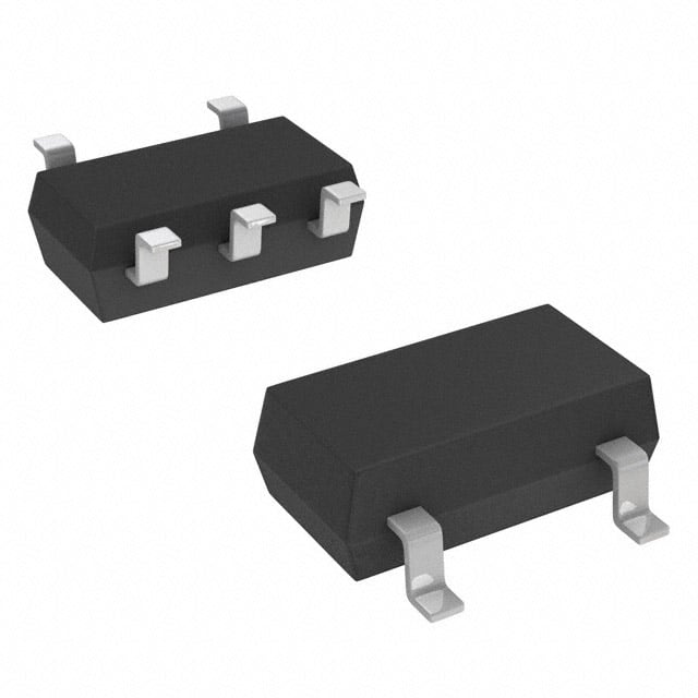
| 描述 | IC OPAMP CUR SENS 125KHZ SOT23-5电流灵敏放大器 Precision 1uA Current Sense Amp |
| DevelopmentKit | MAX9634EVKIT+ |
| 产品分类 | Linear - Amplifiers - Instrumentation, OP Amps, Buffer Amps集成电路 - IC |
| 品牌 | Maxim Integrated |
| 产品手册 | |
| 产品图片 |
|
| rohs | 符合RoHS无铅 / 符合限制有害物质指令(RoHS)规范要求 |
| 产品系列 | 放大器 IC,电流灵敏放大器,Maxim Integrated MAX9634HEUK+T- |
| 数据手册 | |
| 产品型号 | MAX9634HEUK+T |
| 产品培训模块 | http://www.digikey.cn/PTM/IndividualPTM.page?site=cn&lang=zhs&ptm=25703http://www.digikey.cn/PTM/IndividualPTM.page?site=cn&lang=zhs&ptm=25705 |
| 产品种类 | 电流灵敏放大器 |
| 供应商器件封装 | SOT-23-5 |
| 其它名称 | MAX9634HEUK+TDKR |
| 包装 | Digi-Reel® |
| 压摆率 | - |
| 商标 | Maxim Integrated |
| 增益带宽积 | 125kHz |
| 安装类型 | 表面贴装 |
| 安装风格 | SMD/SMT |
| 封装 | Reel |
| 封装/外壳 | SC-74A,SOT-753 |
| 封装/箱体 | SOT-23-5 |
| 工作温度 | -40°C ~ 85°C |
| 工厂包装数量 | 2500 |
| 应用说明 | |
| 放大器类型 | 电流检测 |
| 最大工作温度 | + 85 C |
| 最小工作温度 | - 40 C |
| 标准包装 | 1 |
| 电压-电源,单/双 (±) | - |
| 电压-输入失调 | 100µV |
| 电流-电源 | 1.1µA |
| 电流-输入偏置 | - |
| 电流-输出/通道 | - |
| 电源电压-最大 | +/- 30 V |
| 电路数 | 1 |
| 系列 | MAX9634 |
| 输入电压 | 1.6 v to 26 V |
| 输入补偿电压 | 0.25 mV |
| 输出类型 | - |
| 通道数量 | 1 Channel |
| 零件号别名 | MAX9634 |


- 商务部:美国ITC正式对集成电路等产品启动337调查
- 曝三星4nm工艺存在良率问题 高通将骁龙8 Gen1或转产台积电
- 太阳诱电将投资9.5亿元在常州建新厂生产MLCC 预计2023年完工
- 英特尔发布欧洲新工厂建设计划 深化IDM 2.0 战略
- 台积电先进制程称霸业界 有大客户加持明年业绩稳了
- 达到5530亿美元!SIA预计今年全球半导体销售额将创下新高
- 英特尔拟将自动驾驶子公司Mobileye上市 估值或超500亿美元
- 三星加码芯片和SET,合并消费电子和移动部门,撤换高东真等 CEO
- 三星电子宣布重大人事变动 还合并消费电子和移动部门
- 海关总署:前11个月进口集成电路产品价值2.52万亿元 增长14.8%


PDF Datasheet 数据手册内容提取
EVALUATION KIT AVAILABLE Click here for production status of specific part numbers. MAX9634 nanoPower, 4-Bump UCSP/SOT23, Precision Current-Sense Amplifier General Description Benefits and Features The MAX9634 high-side current-sense amplifier offers ● Ultra-Low Supply Current of 1μA (max) precision accuracy specifications of VOS less than 250μV ● Low 250μV (max) Input Offset Voltage (max) and gain error less than 0.5% (max). Quiescent ● Low < 0.5% (max) Gain Error supply current is an ultra-low 1μA. The MAX9634 fits in a tiny, 1mm x 1mm UCSP™ package size or a 5-pin ● Input Common Mode: +1.6V to +28V SOT23 package, making the part ideal for applications in ● Voltage Output notebook computers, cell phones, PDAs, and all battery- ● Four Gain Versions Available operated portable devices where accuracy, low quiescent • 25V/V (MAX9634T) current, and small size are critical. • 50V/V (MAX9634F) The MAX9634 features an input common-mode voltage • 100V/V (MAX9634H) range from 1.6V to 28V. These current-sense amplifiers • 200V/V (MAX9634W) have a voltage output and are offered in four gain ver- ● Tiny 1mm x 1mm x 0.6mm, 4-Bump UCSP or 5-Pin sions: 25V/V (MAX9634T), 50V/V (MAX9634F), 100V/V SOT23 Packages (MAX9634H), and 200V/V (MAX9634W). The four gain selections offer flexibility in the choice of Ordering Information the external current-sense resistor. The very low 250μV (max) input offset voltage allows small 25mV to 50mV PIN- GAIN TOP PART full-scale VSENSE voltage for very low voltage drop at PACKAGE (V/V) MARK full-current measurement. MAX9634TERS+ 4 UCSP 25 +ABX The MAX9634 is offered in tiny 4-bump UCSP (1mm x MAX9634FERS+ 4 UCSP 50 +ABY 1mm x 0.6mm footprint) and 5-pin SOT23 packages. MAX9634HERS+ 4 UCSP 100 +ABZ Applications MAX9634WERS+ 4 UCSP 200 +ACA ● Cell Phones MAX9634TEUK+ 5 SOT23 25 +AFHG ● PDAs MAX9634FEUK+ 5 SOT23 50 +AFHH ● Power-Management Systems MAX9634HEUK+ 5 SOT23 100 +AFHI ● Portable/Battery-Powered Systems MAX9634WEUK+ 5 SOT23 200 +AFHJ ● Notebook Computers +Denotes a lead(Pb)-free/RoHS-compliant package. Note: All devices except for the MAX9634FEUK+ are specified UCSP is a trademark of Maxim Integrated Products, Inc. over the -40°C to +85°C extended temperature range. The MAX9634FEUK+ is specified over the -40°C to +125°C auto- motive temperature range. Pin Configurations TOP VIEW (BUMPS ON BOTTOM) RS+ RS- 5 4 RS+ A1 A2 RS- MAX9634T/F/H/W MAX9634T/F/H/W GND B1 B2 OUT 1 2 3 UCSP GND GND OUT DRAWINGS NOT TO SCALE SOT23 19-5021; Rev 5; 5/20
MAX9634 nanoPower, 4-Bump UCSP/SOT23, Precision Current-Sense Amplifier Absolute Maximum Ratings RS+, RS- to GND ..................................................-0.3V to +30V Operating Temperature Range ...........................-40°C to +85°C OUT to GND ............................................................-0.3V to +6V Operating Temperature Range (MAX9634FEUK+) RS+ to RS- ..........................................................................±30V ......................................................................-40°C to +125°C Short-Circuit Duration: OUT to GND .........................Continuous Junction Temperature ......................................................+150°C Continuous Input Current (any pin) ..................................±20mA Storage Temperature Range ............................-65°C to +150°C Continuous Power Dissipation (TA = +70°C) Lead Temperature (soldering, 10s) .................................+300°C 4-Bump UCSP (derate 3.0mW/°C above +70°C) ........238mW Soldering Temperature (reflow) .......................................+260°C 5-Pin SOT23 (derate 3.9mW/°C above +70°C) ..........312mW Stresses beyond those listed under “Absolute Maximum Ratings” may cause permanent damage to the device. These are stress ratings only, and functional operation of the device at these or any other conditions beyond those indicated in the operational sections of the specifications is not implied. Exposure to absolute maximum rating conditions for extended periods may affect device reliability. Electrical Characteristics (VRS+ = VRS- = 3.6V, VSENSE = (VRS+ - VRS-) = 0V, TA = -40°C to +85°C, TA (MAX9634FEUK+) = -40°C to +125°C, unless otherwise noted. Typical values are at TA = +25°C.) (Note 1) PARAMETER SYMBOL CONDITIONS MIN TYP MAX UNITS VRS+ = 5V, TA = 0.5 0.85 +25°C VRS+ = 5V, -40°C < 1.1 MAX9634T/MAX9634H/ TA < +85°C µA MAX9634W VRS+ = 28V, TA = 1.1 1.8 +25°C VRS+ = 28V, -40°C < 2.5 TA < +85°C Supply Current (Note 2) ICC VRS+ = 5V, TA = 0.5 0.85 +25°C VRS+ = 5V, -40°C < 1.1 TA < +125°C MAX9634F VRS+ = 28V, TA = 1.1 1.8 +25°C VRS+ = 28V, -40°C < 2.5 TA < +125°C MAX9634T/MAX9634H/ Guaranteed by CMRR, MAX9634W -40°C < TA < +85°C Common-Mode Input Range VCM 1.6 28 V Guaranteed by CMRR, MAX9634F -40°C < TA < +125°C MAX9634T/MAX9634H/ 1.6V < VRS+ < 28V, MAX9634W -40°C < TA < +85°C Common-Mode Rejection Ratio CMRR 94 130 dB 1.6V < VRS+ < 28V, MAX9634F -40°C < TA < +125°C www.maximintegrated.com Maxim Integrated │ 2
MAX9634 nanoPower, 4-Bump UCSP/SOT23, Precision Current-Sense Amplifier Electrical Characteristics (continued) (VRS+ = VRS- = 3.6V, VSENSE = (VRS+ - VRS-) = 0V, TA = -40°C to +85°C, TA (MAX9634FEUK+) = -40°C to +125°C, unless otherwise noted. Typical values are at TA = +25°C.) (Note 1) PARAMETER SYMBOL CONDITIONS MIN TYP MAX UNITS MAX9634T/MAX9634F/ TA = +25°C 100 250 MAX9634H -40°C < TA < +85°C 300 Input Offset Voltage (Note 3) VOS µV TA = +25°C 100 250 MAX9634W -40°C < TA < +85°C 425 MAX9634T 25 MAX9634F 50 Gain G V/V MAX9634H 100 MAX9634W 200 MAX9634T/MAX9634F/ TA = +25°C ±0.1 ±0.5 MAX9634H -40°C < TA < +85°C ±0.6 Gain Error (Note 4) GE % TA = +25°C ±0.1 ±0.7 MAX9634W -40°C < TA < +85°C ±0.8 MAX9634T/MAX9634F/MAX9634H 7.0 10 13.2 Output Resistance (Note 5) ROUT kΩ MAX9634W 14.0 20 26.4 Gain = 25 1.5 7.5 Gain = 50 3 15 OUT Low Voltage VOL mV Gain = 100 6 30 Gain = 200 12 85 MAX9634T/MAX9634H/ VOH = VRS- - VOUT, 0.1 0.2 MAX9634W -40°C < TA < +85°C OUT High Voltage (Note 6) VOH V MAX9634F VOH = VRS- - VOUT, 0.1 0.36 -40°C < TA < +125°C VSENSE = 50mV, gain = 25 125 Small-Signal Bandwidth VSENSE = 50mV, gain = 50 60 BW kHz (Note 5) VSENSE = 50mV, gain = 100 30 VSENSE = 50mV, gain = 200 15 Output Settling Time tS 1% final value, VSENSE = 50mV 100 µs Note 1: All devices are 100% production tested at TA = +25°C. All temperature limits are guaranteed by design. Note 2: VOUT = 0. ICC is the total current into RS+ plus RS- pins. Note 3: VOS is extrapolated from measurements for the gain-error test. Note 4: Gain error is calculated by applying two values of VSENSE and calculating the error of the slope vs. the ideal: Gain = 25, VSENSE is 20mV and 120mV. Gain = 50, VSENSE is 10mV and 60mV. Gain = 100, VSENSE is 5mV and 30mV. Gain = 200, VSENSE is 2.5mV and 15mV. Note 5: The device is stable for any external capacitance value. Note 6: VOH is the voltage from VRS- to VOUT with VSENSE = 3.6V/gain. www.maximintegrated.com Maxim Integrated │ 3
MAX9634 nanoPower, 4-Bump UCSP/SOT23, Precision Current-Sense Amplifier Typical Operating Characteristics (VRS+ = VRS- = 3.6V, TA = +25°C, unless otherwise noted.) SUPPLY CURRENT INPUT OFFSET VOLTAGE HISTOGRAM GAIN ERROR HISTOGRAM vs. TEMPERATURE 2350 MAX9634 toc01 2350 MAX9634 toc02 11..24 28V MAX9634 toc03 A) µ 1.0 20 20 T ( N %) %) RRE 0.8 N ( 15 N ( 15 CU 3.6V Y 0.6 L P 10 10 P SU 0.4 1.8V 5 5 0.2 0 0 0 -0.4 -0.3 -0.2 -0.1 0 0.1 0.2 0.3 0.4 -0.4 -0.3 -0.2 -0.1 0 0.1 0.2 0.3 0.4 -40 -15 10 35 60 85 INPUT OFFSET VOLTAGE (mV) GAIN ERROR (%) TEMPERATURE (°C) INPUT OFFSET INPUT OFFSET SUPPLY CURRENT vs. COMMON-MODE VOLTAGE vs. TEMPERATURE vs. COMMON-MODE VOLTAGE --3350 MAX9634 toc04 5600 MAX9634 toc05 11..24 MAX9634 toc06 A) FFSET (µV) -40 FFSET (µV) 3400 URRENT (µ 10..08 O O C UT -45 UT LY 0.6 NP NP 20 PP I I SU 0.4 -50 10 0.2 -55 0 0 0 5 10 15 20 25 30 -40 -15 10 35 60 85 0 5 10 15 20 25 30 COMMON-MODE VOLTAGE (V) TEMPERATURE (°C) COMMON-MODE VOLTAGE (V) GAIN ERROR GAIN ERROR VOUT vs. VSENSE vs. COMMON-MODE VOLTAGE vs. TEMPERATURE (SUPPLY = 3.6V) 0.01 MAX9634 toc07 00..0078 MAX9634 toc08 34..50 MAX9634 toc09 0.06 3.0 %) -0.1 %) G = 100 ERROR ( -0.2 ERROR (00..0054 (V)OUT 22..05 G = 50 N N V AI AI0.03 1.5 G = 25 G -0.3 G 0.02 1.0 -0.4 0.01 0.5 -0.5 0 0 0 5 10 15 20 25 30 -40 -15 10 35 60 85 0 50 100 150 VOLTAGE (V) TEMPERATURE (°C) VSENSE (mV) www.maximintegrated.com Maxim Integrated │ 4
MAX9634 nanoPower, 4-Bump UCSP/SOT23, Precision Current-Sense Amplifier Typical Operating Characteristics (continued) (VRS+ = VRS- = 3.6V, TA = +25°C, unless otherwise noted.) VOUT vs. VSENSE SMALL-SIGNAL GAIN CMRR (SUPPLY = 1.6V) vs. FREQUENCY vs. FREQUENCY 111...468 MAX9634 toc10 -505 AAVV == 12050VV/V/V MAX9634 toc11 --42000 G = 25 MAX9634 toc12 1.2 G = 50 V (V)OUT 01..80 G =G 5 =0 100 GAIN (dB) --1105 AV = 50V/V CMRR (dB) --6800 -100 G = 100 0.6 G = 25 -20 -120 0.4 0.2 -25 -140 0 -30 -160 0 20 40 60 80 100 1 10 100 1k 10k 100k 1M 1 10 100 1k 10k 100k 1M VSENSE (mV) FREQUENCY (Hz) FREQUENCY (Hz) SMALL-SIGNAL PULSE RESPONSE SMALL-SIGNAL PULSE RESPONSE SMALL-SIGNAL PULSE RESPONSE (GAIN = 100) (GAIN = 50) (GAIN = 25) MAX9634 toc13a MAX9634 toc13b MAX9634 toc13c 15mV 30mV 60mV VSENSE 10mV VSENSE 20mV VSENSE 40mV 1.5V 1.5V 1.5V VOUT VOUT 1V VOUT 1V 1V 20µs/div 25µs/div 25µs/div LARGE-SIGNAL PULSE RESPONSE LARGE-SIGNAL PULSE RESPONSE LARGE-SIGNAL PULSE RESPONSE (GAIN = 100) (GAIN = 50) (GAIN = 25) MAX9634 toc14a MAX9634 toc14b MAX9634 toc14c 30mV 60mV 120mV VSENSE VSENSE VSENSE 10mV 10mV 20mV 3V 3V 3V VOUT VOUT VOUT 0.5V 1V 0.5V 20µs/div 25µs/div 25µs/div www.maximintegrated.com Maxim Integrated │ 5
MAX9634 nanoPower, 4-Bump UCSP/SOT23, Precision Current-Sense Amplifier Pin Description PIN NAME FUNCTION UCSP SOT23 A1 5 RS+ External Sense Resistor Power-Side Connection A2 4 RS- External Sense Resistor Load-Side Connection B1 1, 2 GND Ground B2 3 OUT Output Voltage. VOUT is proportional to VSENSE = VRS+ - VRS-. Typical Operating Circuit ILOAD RSENSE VBATT = 1.6V TO 28V RS+ RS- R1 R1 VDD = 3.3V LOAD µC P MAX9634 OUT ADC ROUT 10kΩ GND www.maximintegrated.com Maxim Integrated │ 6
MAX9634 nanoPower, 4-Bump UCSP/SOT23, Precision Current-Sense Amplifier Detailed Description pin. Therefore, the OUT voltage swing is limited by the minimum voltage at RS+. The MAX9634 unidirectional high-side, current-sense amplifier features a 1.6V to 28V input common-mode VOUT (max) = VRS+ (min) - VSENSE (max) - VOH range. This feature allows the monitoring of current out and: of a battery with a voltage as low as 1.6V. The MAX9634 monitors current through a current-sense resistor and R = VOUT(max) SENSE amplifies the voltage across that resistor. G×I (max) LOAD The MAX9634 is a unidirectional current-sense amplifier that has a well-established history. An op amp is used VSENSE full scale should be less than VOUT/GAIN at the minimum RS+ voltage. For best performance with a 3.6V to force the current through an internal gain resistor at RS+, which has a value of R1, such that its voltage drop supply voltage, select RSENSE to provide approximately 120mV (gain of 25V/V), 60mV (gain of 50V/V), 30mV (gain equals the voltage drop across an external sense resis- of 100V/V), or 15mV (gain of 200V/V) of sense voltage for tor, RSENSE. There is an internal resistor at RS- with the the full-scale current in each application. These can be same value as R1 to minimize offset voltage. The current increased by use of a higher minimum input voltage. through R1 is sourced by a high-voltage p-channel FET. Its source current is the same as its drain current, which Accuracy flows through a second gain resistor, ROUT. This produc- In the linear region (VOUT < VOUT (max)), there are two es an output voltage, VOUT, whose magnitude is ILOAD components to accuracy: input offset voltage (VOS) and x RSENSE x ROUT/R1. The gain accuracy is based on gain error (GE). For the MAX9634, VOS = 250μV (max) the matching of the two gain resistors R1 and ROUT (see and gain error is 0.5% (max). Use the linear equation: Table 1). Total gain = 25V/V for the MAX9634T, 50V/V for the MAX9634F, 100V/V for the MAX9634H, and 200V/V VOUT = (gain ± GE) x VSENSE ± (gain x VOS) for the MAX9634W. The output is protected from input to calculate total error. A high RSENSE value allows lower overdrive by use of an output current-limiting circuit of currents to be measured more accurately because offsets 7mA (typical) and a 6V clamp protection circuit. are less significant when the sense voltage is larger. Efficiency and Power Dissipation Applications Information At high current levels, the I2R losses in RSENSE can be Choosing the Sense Resistor significant. Take this into consideration when choosing the Choose RSENSE based on the following criteria: resistor value and its power dissipation (wattage) rating. Also, the sense resistor’s value might drift if it is allowed to Voltage Loss heat up excessively. The precision VOS of the MAX9634 A high RSENSE value causes the power-source voltage allows the use of small sense resistors to reduce power to drop due to IR loss. For minimal voltage loss, use the dissipation and reduce hot spots. lowest RSENSE value. Kelvin Connections OUT Swing vs. VRS+ and VSENSE Because of the high currents that flow through RSENSE, The MAX9634 is unique because the supply voltage is take care to eliminate parasitic trace resistance from the input common-mode voltage (the average voltage at causing errors in the sense voltage. Either use a four- RS+ and RS-). There is no separate VCC supply voltage terminal current-sense resistor or use Kelvin (force and sense) PCB layout techniques. Table 1. Internal Gain-Setting Resistors Optional Output Filter Capacitor (Typical Values) When designing a system that uses a sample-and-hold stage in the ADC, the sampling capacitor momentarily GAIN R1 ROUT loads OUT and causes a drop in the output voltage. If (V/V) (Ω) (kΩ) sampling time is very short (less than a microsecond), 200 100 20 consider using a ceramic capacitor across OUT and 100 100 10 GND to hold VOUT constant during sampling. This also 50 200 10 decreases the small-signal bandwidth of the current- sense amplifier and reduces noise at OUT. 25 400 10 www.maximintegrated.com Maxim Integrated │ 7
MAX9634 nanoPower, 4-Bump UCSP/SOT23, Precision Current-Sense Amplifier ILOAD RSENSE TO WALL-CUBE/ VBATT = 1.6V TO 28V CHARGER RS+ RS- RS+ RS- LOAD R1 R1 R1 R1 P P MAX9634 MAX9634 VDD = 3.3V OUT OUT ROUT 10kΩ ROUT 10kΩ µC GND GND ADC ADC Figure 1. Bidirectional Application Bidirectional Application UCSP Applications Information Battery-powered systems may require a precise bidirec- For the latest application details on UCSP construction, tional current-sense amplifier to accurately monitor the dimensions, tape carrier information, PCB techniques, battery’s charge and discharge currents. Measurements bump-pad layout, and recommended reflow temperature of the two separate outputs with respect to GND yields an profile, as well as the latest information on reliability test- accurate measure of the charge and discharge currents, ing results, refer to Application Note 1891: Wafer-Level respectively (Figure 1). Packaging (WLP) and Its Applications. Chip Information Package Information PROCESS: BiCMOS For the latest package outline information and land patterns (footprints), go to www.maximintegrated.com/packages. Note that a “+”, “#”, or “-” in the package code indicates RoHS status only. Package drawings may show a different suffix character, but the drawing pertains to the package regardless of RoHS status. PACKAGE PACKAGE OUTLINE LAND TYPE CODE NO. PATTERN NO. 2 x 2 UCSP R41A1+1 21-0242 — 5 SOT23 U5-2 21-0057 90-0174 www.maximintegrated.com Maxim Integrated │ 8
MAX9634 nanoPower, 4-Bump UCSP/SOT23, Precision Current-Sense Amplifier Revision History REVISION REVISION PAGES DESCRIPTION NUMBER DATE CHANGED 0 10/09 Initial release — 1 2/10 Corrected gain error limits in Electrical Characteristics table 2 2 8/10 Removed Power-Up Time parameter 3 3 3/17 Updated title to include “nanoPower” and updated package outline drawing 1–11 4 7/19 Updated TOC04 and TOC05 4 Updated General Description, Ordering Information note, Absolute Maximum Ratings, 5 5/20 1, 2, 3 and Electrical Characteristics table; fixed links For pricing, delivery, and ordering information, please visit Maxim Integrated’s online storefront at https://www.maximintegrated.com/en/storefront/storefront.html. Maxim Integrated cannot assume responsibility for use of any circuitry other than circuitry entirely embodied in a Maxim Integrated product. No circuit patent licenses are implied. Maxim Integrated reserves the right to change the circuitry and specifications without notice at any time. The parametric values (min and max limits) shown in the Electrical Characteristics table are guaranteed. Other parametric values quoted in this data sheet are provided for guidance. Maxim Integrated and the Maxim Integrated logo are trademarks of Maxim Integrated Products, Inc. © 2020 Maxim Integrated Products, Inc. │ 9