ICGOO在线商城 > 集成电路(IC) > 接口 - 驱动器,接收器,收发器 > AD8123ACPZ
 Datasheet下载
- 型号: AD8123ACPZ
- 制造商: Analog
- 库位|库存: xxxx|xxxx
- 要求:
| 数量阶梯 | 香港交货 | 国内含税 |
| +xxxx | $xxxx | ¥xxxx |
查看当月历史价格
查看今年历史价格
AD8123ACPZ产品简介:
ICGOO电子元器件商城为您提供AD8123ACPZ由Analog设计生产,在icgoo商城现货销售,并且可以通过原厂、代理商等渠道进行代购。 AD8123ACPZ价格参考。AnalogAD8123ACPZ封装/规格:接口 - 驱动器,接收器,收发器, 接收器 0/3 40-LFCSP-WQ(6x6)。您可以下载AD8123ACPZ参考资料、Datasheet数据手册功能说明书,资料中有AD8123ACPZ 详细功能的应用电路图电压和使用方法及教程。
AD8123ACPZ 是由 Analog Devices Inc. 生产的一款接口驱动器、接收器和收发器。该器件主要用于高速信号传输和处理应用,特别是在视频和图像处理领域。

 应用场景

1. 视频信号传输:
   AD8123ACPZ 适用于需要高带宽和低延迟的视频信号传输系统。它可以用于将模拟视频信号转换为数字信号,或反之亦然,确保信号在传输过程中保持高质量。常见的应用场景包括高清电视(HDTV)、专业视频设备、医疗成像系统等。

2. 显示接口:
   该芯片可以作为显示器与信号源之间的接口,支持多种视频标准,如VGA、DVI、HDMI等。它能够有效地驱动长距离电缆,减少信号衰减和噪声干扰,从而提高显示质量。

3. 工业自动化:
   在工业控制系统中,AD8123ACPZ 可以用于实现高速数据通信,例如在工厂自动化、机器人控制等领域。它能够提供稳定的信号传输,确保控制系统中的数据准确无误地传递。

4. 测试与测量设备:
   对于需要精确信号传输的测试与测量设备,AD8123ACPZ 可以确保信号的完整性和准确性。它广泛应用于示波器、频谱分析仪等仪器中,帮助工程师进行精确的信号分析和故障诊断。

5. 通信系统:
   在通信基础设施中,AD8123ACPZ 可以用于高速数据传输,特别是在光纤通信和无线通信系统中。它能够处理复杂的信号调制和解调,确保数据传输的可靠性和速度。

6. 消费电子:
   在消费电子产品中,AD8123ACPZ 可以用于连接各种多媒体设备,如蓝光播放器、游戏机、投影仪等。它能够提供高质量的音频和视频信号传输,提升用户的娱乐体验。

 总结

AD8123ACPZ 凭借其卓越的性能和广泛的适用性,在多个领域中发挥着重要作用。无论是视频信号传输、显示接口、工业自动化,还是测试与测量设备,它都能提供稳定、高效的数据传输解决方案。
| 参数 | 数值 |
| 3dB带宽 | 120 MHz |
| 产品目录 | 集成电路 (IC)半导体 |
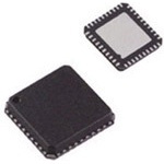
| 描述 | IC RCVR TRPL DIFF EQUAL 40LFCSP视频放大器 Trple Diff Rcvr w/ Adj Line Equal |
| 产品分类 | |
| 品牌 | Analog Devices Inc |
| 产品手册 | |
| 产品图片 |
|
| rohs | 符合RoHS无铅 / 符合限制有害物质指令(RoHS)规范要求 |
| 产品系列 | 放大器 IC,视频放大器,Analog Devices AD8123ACPZ- |
| 数据手册 | |
| 产品型号 | AD8123ACPZ |
| PCN组件/产地 | |
| 产品 | Video Amplifiers |
| 产品种类 | 视频放大器 |
| 供应商器件封装 | 40-LFCSP-VQ(6x6) |
| 包装 | 托盘 |
| 协议 | - |
| 双工 | - |
| 可用增益调整 | 55 dB |
| 商标 | Analog Devices |
| 安装类型 | 表面贴装 |
| 安装风格 | SMD/SMT |
| 封装 | Tray |
| 封装/外壳 | 40-VFQFN 裸露焊盘,CSP |
| 封装/箱体 | LFCSP-40 |
| 工作温度 | -40°C ~ 85°C |
| 工作温度范围 | - 40 C to + 85 C |
| 工作电源电压 | 4.5 V to 5.5 V |
| 工厂包装数量 | 490 |
| 带宽 | 120 MHz |
| 接收器滞后 | 70mV |
| 数据速率 | - |
| 最大工作温度 | + 85 C |
| 最小工作温度 | - 40 C |
| 标准包装 | 1 |
| 电压-电源 | ±4.5 V ~ 5.5 V |
| 电压增益dB | 55 dB |
| 电源电压-最大 | 5.5 V |
| 电源电压-最小 | 4.5 V |
| 电源电流 | 132 mA |
| 电源类型 | Single |
| 类型 | 接收器 |
| 系列 | AD8123 |
| 通道数量 | 3 Channel |
| 驱动器/接收器数 | 0/3 |


PDF Datasheet 数据手册内容提取
Triple Differential Receiver with Adjustable Line Equalization Data Sheet AD8123 FEATURES FUNCTIONAL BLOCK DIAGRAM Compensates cables to 300 meters for wideband video VPEAK VPOLE VOFFSET VGAIN Fast rise and fall times AD8123 4.9 ns with 2 V step at 150 meters of UTP cable 8.0 ns with 2 V step at 300 meters of UTP cable –INR 55 dB peak gain at 100 MHz OUTR +INR Two frequency response gain adjustment pins High frequency peaking adjustment (VPEAK) –ING Broadband flat gain adjustment (V ) OUTG GAIN +ING Pole location adjustment pin (V ) POLE Compensates for variations between cables –INB OUTB Can be optimized for either UTP or coaxial cable +INB DC output offset adjust (V ) OFFSET Low output offset voltage: 24 mV –INCMP1 OUTCMP1 Compensates both RGB and YPbPr +INCMP1 Two on-chip comparators with hysteresis –INCMP2 AvCaailna bblee uins e4d0 -floera cdo, m6 mmomn ×-m 6o mdme s LyFnCcS ePx t raction +INCMP2 OUTCMP2 06814-001 Figure 1. APPLICATIONS Keyboard-video-mouse (KVM) Digital signage RGB video over UTP cables Professional video projection and distribution HD video Security video GENERAL DESCRIPTION For added flexibility, an optional pole adjustment pin, V , POLE allows movement of the pole locations, allowing for the The AD8123 is a triple, high speed, differential receiver and compensation of different gauges and types of cable as well equalizer that compensates for the transmission losses of UTP as variations between different cables and/or equalizers. The and coaxial cables up to 300 meters in length. Various gain V pin allows the dc voltage at the output to be adjusted, stages are summed together to best approximate the inverse OFFSET adding flexibility for dc-coupled systems. frequency response of the cable. Logic circuitry inside the AD8123 controls the gain functions of the individual stages so that the The AD8123 is available in a 6 mm × 6 mm, 40-lead LFCSP lowest noise can be achieved at short-to-medium cable lengths. and is rated to operate over the extended temperature range of This technique optimizes its performance for low noise, short- −40°C to +85°C. to-medium range applications, while at the same time provides UXGA RESOLUTION IMAGE UXGA RESOLUTION IMAGE AFTER 300 METER CAT-5 CABLE AFTER 300 METER CAT-5 CABLE the high gain bandwidth required for long cable equalization BEFORE AD8123. AFTER AD8123. (up to 300 meters). Each channel features a high impedance differential input that is ideal for interfacing directly with the cable. The AD8123 has three control pins for optimal cable compensation, as well as an output offset adjust pin. Two vcaobltlae gleen-cgothnst;r tohllee Vd PpEAinK sp ainre c ounsetrdo ltso t choe mampeonusnatt oe ff ohrig dhi fffreerqeunetn cy 06814-019 peaking and the V pin adjusts the broadband flat gain, Figure 2. UXGA Resolution Images Before and After the AD8123 GAIN which compensates for the low frequency flat cable loss. Rev. B Document Feedback Information furnished by Analog Devices is believed to be accurate and reliable. However, no responsibility is assumed by Analog Devices for its use, nor for any infringements of patents or other One Technology Way, P.O. Box 9106, Norwood, MA 02062-9106, U.S.A. rights of third parties that may result from its use. Specifications subject to change without notice. No license is granted by implication or otherwise under any patent or patent rights of Analog Devices. Tel: 781.329.4700 ©2007–2016 Analog Devices, Inc. All rights reserved. Trademarks and registered trademarks are the property of their respective owners. Technical Support www.analog.com
AD8123 Data Sheet TABLE OF CONTENTS Features .............................................................................................. 1 Comparators ............................................................................... 11 Applications ....................................................................................... 1 Sync Pulse Extraction Using Comparators ............................. 12 Functional Block Diagram .............................................................. 1 Using the V , V , V , and V Inputs ................... 12 PEAK POLE GAIN OFFSET General Description ......................................................................... 1 Using the AD8123 with Coaxial Cable .................................... 13 Revision History ............................................................................... 2 Driving 75 Ω Video Cable With the AD8123 ........................ 13 Specifications ..................................................................................... 3 Driving a Capacitive Load ......................................................... 13 Absolute Maximum Ratings ............................................................ 5 Filtering the RGB Outputs ........................................................ 13 Thermal Resistance ...................................................................... 5 Power Supply Filtering ............................................................... 14 ESD Caution .................................................................................. 5 Layout and Power Supply Decoupling Considerations ......... 14 Pin Configuration and Function Descriptions ............................. 6 Input Common-Mode Range ................................................... 15 Typical Performance Characteristics ............................................. 7 Small Signal Frequency Response ............................................ 15 Theory of Operation ...................................................................... 10 Power-Down ............................................................................... 15 Input Common-Mode Voltage Range Considerations ......... 10 Outline Dimensions ....................................................................... 16 Applications Information .............................................................. 11 Ordering Guide .......................................................................... 16 Basic Operation .......................................................................... 11 REVISION HISTORY 1/16— Rev. A to Rev. B Added Figure 2 Caption................................................................... 1 Changes to Figure 4 and Table 4 ..................................................... 6 Updated Outline Dimensions ....................................................... 16 Changes to Ordering Guide .......................................................... 16 11/07—Rev. 0 to Rev. A Changes to Features .......................................................................... 1 Changes to Ordering Guide .......................................................... 16 8/07—Revision 0: Initial Version Rev. B | Page 2 of 16
Data Sheet AD8123 SPECIFICATIONS T = 25°C, V = ±5 V, R = 150 Ω, Belden Cable (BL-7987R), V = 0 V, V , V , and V are set to recommended settings shown in A S L OFFSET PEAK GAIN POLE Figure 17, unless otherwise noted. Table 1. Parameter Test Conditions/Comments Min Typ Max Unit PEAKING PERFORMANCE (NO CABLE) Peak Frequency V = 2 V, V = 0.6 V, V = 1 V 100 MHz PEAK GAIN POLE V = 2 V, V = 0.6 V, V = 2 V 105 MHz PEAK GAIN POLE Peak Gain V = 2 V, V = 0.6 V, V = 1 V 45 dB PEAK GAIN POLE V = 2 V, V = 0.6 V, V = 2 V 55 dB PEAK GAIN POLE DYNAMIC PERFORMANCE 10% to 90% Rise/Fall Time V = 2 V step, 150 meters Cat-5 4.9 ns OUT V = 2 V step, 300 meters Cat-5 8.0 ns OUT Settling Time to 2% V = 2 V step, 150 meters Cat-5 36 ns OUT V = 2 V step, 300 meters Cat-5 106 ns OUT –3 dB Large Signal Bandwidth V = 1 V p-p, <10 meters Cat-5 120 MHz OUT V = 2 V p-p, <10 meters Cat-5 110 MHz OUT V = 2 V p-p, 150 meters Cat-5 78 MHz OUT V = 2 V p-p, 300 meters Cat-5 43 MHz OUT Integrated Output Voltage Noise 150 meter setting, integrated to 160 MHz 2.5 mV rms 300 meter setting, integrated to 160 MHz 24 mV rms INPUT DC PERFORMANCE Input Voltage Range −IN and +IN ±3.0 V Maximum Differential Voltage Swing 4 V p-p Voltage Gain ΔV /ΔV, V set for 0 meters of cable 1 V/V O I GAIN Common-Mode Rejection Ratio (CMRR) At dc, V = V = V = 0 V −86 dB PEAK GAIN POLE At dc, V = V = V = 2 V −67 dB PEAK GAIN POLE At 1 MHz, V = V = V = 2 V −52 dB PEAK GAIN POLE Input Resistance Common mode 4.4 MΩ Differential 3.7 MΩ Input Capacitance Common mode 1.0 pF Differential 0.5 pF Input Bias Current 2.4 µA V Pin Current 28.9 µA OFFSET V Pin Current 0.5 µA GAIN V Pin Current 0.4 µA PEAK V Pin Current 0.4 µA POLE ADJUSTMENT PINS V Input Voltage Range Relative to GND 0 to 2 V PEAK V Input Voltage Range Relative to GND 0 to 2 V POLE V Input Voltage Range Relative to GND 0 to 2 V GAIN V to OUT Gain OUT/V , range limited by output swing 1 V/V OFFSET OFFSET Maximum Flat Gain V = 2 V 2 dB GAIN OUTPUT CHARACTERISTICS Output Voltage Swing 150 Ω load −3.75 to +3.69 V 1 kΩ load −3.66 to +3.69 V Output Offset Voltage Referred to output, V = V = V = 0 V 24 mV PEAK GAIN POLE Referred to output, V = V = V = 2 V 32 mV PEAK GAIN POLE Output Offset Voltage Drift Referred to output 33 µV/°C Rev. B | Page 3 of 16
AD8123 Data Sheet Parameter Test Conditions/Comments Min Typ Max Unit POWER SUPPLY Operating Voltage Range ±4.5 ±5.5 V Positive Quiescent Supply Current 132 mA Negative Quiescent Supply Current 126 mA Supply Current Drift, I /I 80 µA/°C CC EE Positive Power Supply Rejection Ratio DC, referred to output −51 dB Negative Power Supply Rejection Ratio DC, referred to output −63 dB Power Down, V (Minimum) Minimum Logic 1 voltage 1.1 V IH Power Down, V (Maximum) Maximum Logic 0 voltage 0.8 V IL Positive Supply Current, Powered Down V = V = V = 0 V 1.1 µA PEAK GAIN POLE Negative Supply Current, Powered Down V = V = V = 0 V 0.7 µA PEAK GAIN POLE COMPARATORS Output Voltage Levels V /V 3.33/0.043 V OH OL Hysteresis V 70 mV HYST Propagation Delay t /t 17.5/10.0 ns PD, LH PD, HL Rise/Fall Times t /t 9.3/9.3 ns RISE FALL Output Resistance 0.03 Ω OPERATING TEMPERATURE RANGE −40 +85 °C Rev. B | Page 4 of 16
Data Sheet AD8123 ABSOLUTE MAXIMUM RATINGS The power dissipated in the package (P ) is the sum of the D Table 2. quiescent power dissipation and the power dissipated in the Parameter Rating package due to the load drive for all outputs. The quiescent Supply Voltage 11 V power is the voltage between the supply pins (V) times the S Power Dissipation See Figure 3 quiescent current (I). The power dissipation due to each load S Input Voltage (Any Input) V − 0.3 V to V + 0.3 V S− S+ current is calculated by multiplying the load current by the Storage Temperature Range −65°C to +125°C voltage difference between the associated power supply and the Operating Temperature Range −40°C to +85°C output voltage. The total power dissipation due to load currents Lead Temperature (Soldering, 10 sec) 300°C is then obtained by taking the sum of the individual power Junction Temperature 150°C dissipations. RMS output voltages must be used when dealing with ac signals. Stresses at or above those listed under Absolute Maximum Ratings may cause permanent damage to the product. This is a Airflow reduces θ . In addition, more metal directly in contact JA stress rating only; functional operation of the product at these with the package leads from metal traces, through holes, ground, or any other conditions above those indicated in the operational and power planes reduces the θ . The exposed paddle on the JA section of this specification is not implied. Operation beyond underside of the package must be soldered to a pad on the PCB the maximum operating conditions for extended periods may surface that is thermally connected to a solid plane (usually the affect product reliability. ground plane) to achieve the specified θ . JA THERMAL RESISTANCE Figure 3 shows the maximum safe power dissipation in the package vs. the ambient temperature for the 40-lead LFCSP θ is specified for the worst-case conditions, that is, θ is JA JA (29°C/W) on a JEDEC standard 4-layer board with the underside specified for the device soldered in a circuit board in still air. paddle soldered to a pad that is thermally connected to a PCB Table 3. Thermal Resistance with the Underside Pad plane. θ values are approximations. JA Connected to the Plane 7 Package Type/PCB Type θ Unit JA 40-Lead LFCSP/4-Layer 29 °C/W W) 6 N ( O Maximum Power Dissipation TI 5 A P The maximum safe power dissipation in the AD8123 package SI S 4 is limited by the associated rise in junction temperature (TJ) on R DI E the die. At approximately 150°C, which is the glass transition W 3 O temperature, the plastic changes its properties. Even temporarily M P exceeding this temperature limit can change the stresses that the MU 2 XI package exerts on the die, permanently shifting the parametric A M 1 performance of the AD8123. Exceeding a junction temperature of 175°C for an extended time can result in changes in the 0 silicon devices, potentially causing failure. –40 –20 AMB0IENT TE2M0PERATU4R0E (°C) 60 80 06814-025 Figure 3. Maximum Power Dissipation vs. Temperature for a 4-Layer Board ESD CAUTION Rev. B | Page 5 of 16
AD8123 Data Sheet PIN CONFIGURATION AND FUNCTION DESCRIPTIONS AD8123 TOP VIEW (Not to Scale) NICGND–INB+INBVS+–ING+INGVS––INR+INR 0987654321 4333333333 NIC 1 30 NIC +–IINNCCMMPP11 23 1 2289 VPSD+ OUTCMP1 4 27 VPOLE VS+_CMP 5 26 VPEAK OUTCMP2 6 25 VGAIN –INCMP2 7 2 24 GND +INCMP2 8 23 VOFFSET VS–_CMP 9 22 VS– NIC10 21 NIC 1234567890 1111111112 VS–UTBVS+VS–UTGVS+VS–UTRVS+NIC O O O NOTES 1. NIC = NO INTERNAL CONNECTION. 2 . EMSXPUPESOCTIS FBEIEED DC P OTAHNDENDRELMCETA OELND R TTEHOSEI AS BT POACTNBTC OPEML.A ONFE TTHOE A PCAHCIEKVAEGE 06814-002 Figure 4. Pin Configuration Table 4. Pin Function Descriptions Pin No. Mnemonic Description 1, 10, 20, 21, 30, 40 NIC No Internal Connection. 2 +IN Positive Input, Comparator 1. CMP1 3 −IN Negative Input, Comparator 1. CMP1 4 OUT Output, Comparator 1. CMP1 5 V _CMP Positive Power Supply, Comparator. Must be connected to V . S+ S+ 6 OUT Output, Comparator 2. CMP2 7 −IN Negative Input, Comparator 2. CMP2 8 +IN Positive Input, Comparator 2. CMP2 9 V _CMP Negative Power Supply, Comparator. Must be connected to V . S− S− 11, 14, 17, 22, 33 V Negative Power Supply, Equalizer Sections. S− 12 OUT Output, Blue Channel. B 13, 16, 19, 29, 36 V Positive Power Supply, Equalizer Sections. S+ 15 OUT Output, Green Channel. G 18 OUT Output, Red Channel. R 23 V Output Offset Control Voltage. OFFSET 24, 39 GND Signal Ground Reference. 25 V Broadband Flat Gain Control Voltage. GAIN 26 V Equalizer High Frequency Boost Control Voltage. PEAK 27 V Equalizer Pole Location Adjustment Control Voltage. POLE 28 PD Power Down. 31 +IN Positive Input, Red Channel. R 32 −IN Negative Input, Red Channel. R 34 +IN Positive Input, Green Channel. G 35 −IN Negative Input, Green Channel. G 37 +IN Positive Input, Blue Channel. B 38 −IN Negative Input, Blue Channel. B EPAD Exposed Paddle. Exposed paddle on the bottom of the package must be connected to a PCB plane to achieve specified thermal resistance. Rev. B | Page 6 of 16
Data Sheet AD8123 TYPICAL PERFORMANCE CHARACTERISTICS T = 25°C, V = ±5 V, R = 150 Ω, Belden Cable (BL-7987R), V = 0 V, V , V , and V are set to recommended settings shown in A S L OFFSET PEAK GAIN POLE Figure 17, unless otherwise noted. 4 3 3 VVGPOALINE == 00VV 2 VO = 2V p-p VO = 1V p-p 1 2 0 –1 1 –2 B) 0 B) –3 N (d –1 N (d –4 AI AI –5 G –2 G –6 –7 –3 –8 –4 –9 5100m0m VGAIN = 0V –10 150m –5 VGAIN = 1V 200m VGAIN = 2V –11 300m –6100k 1M FREQUENC1Y0 (MHz) 100M 06814-003 –12100k 1M FREQUENC1Y0 (MHz) 100M 06814-006 Figure 5. Frequency Response for Various VGAIN Without Cable Figure 8. Equalized Frequency Response for Various Cable Lengths 60 120 VGAIN = 0.6V VO = 2V p-p VPOLE = 2V 40 VO = 1V p-p 100 20 Hz) 80 M AIN (dB) 0 WIDTH ( 60 G D N –20 BA 40 –40 20 VPEAK = 0V VPEAK = 1V –60100k VPEAK = 2V 1M FREQUENC1Y0 (MHz) 100M 06814-004 00 50 C1A0B0LE LEN1G5T0H (meter2s0)0 250 300 06814-007 Figure 6. Frequency Response for Various VPEAK Without Cable Figure 9. Equalized −3 dB Bandwidth vs. Cable Length 40 6 30 VVVGPOE A=AIN K1 V== 0p1.-V6pV 4 VVVGPPEOAALINKE === 000.VV6V 20 10 2 B) 0 E (V) AIN (d –10 LTAG 0 G –20 VO –2 –30 –40 –4 –50 VVVPPPOOOLLLEEE === 012VVV IONUPTUPTUT –60100k 1M FREQUENC1Y0 (MHz) 100M 06814-005 –60 50 100 150 200TIM2E5 0(ns)300 350 400 450 500 06814-008 Figure 7. Frequency Response for Various VPOLE Without Cable Figure 10. Overdrive Recovery Rev. B | Page 7 of 16
AD8123 Data Sheet 1.5 1.5 50m 50m 150m 150m 300m 1.0 300m 1.0 V) V) E ( 0.5 E ( 0.5 G G A A T T L L O 0 O 0 V V T T U U P P UT–0.5 UT–0.5 O O –1.0 –1.0 –1.50 50 100 150 200TIM2E5 0(ns)300 350 400 450 500 06814-009 –1.50 1 2 3 4TIME5 (µs)6 7 8 9 10 06814-012 Figure 11. Pulse Response for Various Cable Lengths (2 MHz) Figure 14. Pulse Response for Various Cable Lengths (100 kHz) 10000 30 0m M 150m RO 300m F Hz) SE 25 UTPUT VOLTAGE NOISE (nV/ 1010000 ATED OUTPUT VOLTAGE NOI100kHz TO 160MHz (mV rms)112050 O R 5 G E T N I 10100k 1M FREQUENCY10 (MHz) 100M 06814-010 025 50 75 100CA1B2L5E L1E50NGT17H5 (m2e0te0rs)225 250 275 300 06814-013 Figure 12. Output Voltage Noise vs. Frequency for Various Cable Length Figure 15. Integrated Output Voltage Noise vs. Cable Length 20 20 10 VVGGAAIINN == 01V.8, 5VVP,E VAPKE =A K0 V=, 1V.6P5OVLE, V=P 0OVLE = 1.75V 10 VVGGAAIINN == 01V.8, 5VVP,E VAPKE =A K0 V=, 1V.6P5OVLE, V=P 0OVLE = 1.75V 0 0 –10 –10 MRR (dB) –––432000 SSTALK (dB) ––3200 C O –40 –50 R C –50 –60 –70 –60 –80 –70 –90100k 1M FREQUENC1Y0 (MHz) 100M 06814-011 –80100k 1M FREQUENC1Y0 (MHz) 100M 06814-014 Figure 13. CMRR vs. Frequency Figure 16. Crosstalk vs. Frequency Rev. B | Page 8 of 16
Data Sheet AD8123 2.0 2.0 VPEAK VPEAK 1.8 VVPGOALINE 1.8 VVPGOALINE 1.6 1.6 E (V) 1.4 E (V) 1.4 G G A 1.2 A 1.2 T T L L VO 1.0 VO 1.0 L L RO 0.8 RO 0.8 T T N N O 0.6 O 0.6 C C 0.4 0.4 0.2 0.2 025 50 75 100CA1B2L5E L1E50NGT17H5 (m2e0te0rs)225 250 275 300 06814-015 025 50 75 100CA1B2L5E L1E50NGT17H5 (m2e0te0rs)225 250 275 300 06814-016 Figure 17. Recommended Settings for UTP Cable Figure 18. Recommended Settings for Coaxial Cable Rev. B | Page 9 of 16
AD8123 Data Sheet THEORY OF OPERATION The AD8123 is a unity-gain, triple, wideband, low noise analog The AD8123 is designed such that systems that use short-to- line equalizer that compensates for losses in UTP and coaxial medium-length cables do not pay a noise penalty for excess gain cables up to 300 meters in length. The 3-channel architecture is that they do not require. The high gain is only available for targeted at high resolution RGB applications but can be used in longer length systems where it is required. This feature is built HD YPbPr applications as well. into the V control and is transparent to the user. PEAK Three continuously adjustable control voltages, common Two comparators are provided on-chip that can be used for to the RGB channels, are available to the designer to provide sync pulse extraction in systems that use sync-on-common compensation for various cable lengths as well as for variations mode encoding. Each comparator has very low output impedance in the cable itself. The V input is used to control the amount and can therefore be used in a source-only cable termination PEAK of high frequency peaking. V is the primary control that is scheme by placing a series resistor equal to the cable characteristic PEAK used to compensate for frequency and cable-length dependent, impedance directly on the comparator output. Additional high frequency losses that are present due to the skin effect of details are provided in the Applications Information section. the cable. A second control pin, VGAIN, is used to adjust broadband INPUT COMMON-MODE VOLTAGE RANGE gain to compensate for low frequency flat losses present in the CONSIDERATIONS cable. A third control, V , is used to move the positions of the POLE When using the AD8123 as a receiver, it is important to ensure equalizer poles and can be linearly derived from V , as illustrated PEAK that its input common-mode voltage stays within the specified in the Typical Performance Characteristics and Applications range. The received common-mode level is calculated by adding Information sections, for UTP and coaxial cables. Finally, an the common-mode level of the driver, the single-ended peak output offset adjust control, V , allows the designer to shift OFFSET amplitude of the received signal, the amplitude of any sync the output dc level. pulses, and the other induced common-mode signals, such as The AD8123 has a high impedance differential input that makes ground shifts between the driver and the AD8123 and pickup termination simple and allows dc-coupled signals to be received from external sources, such as power lines and fluorescent directly from the cable. The AD8123 input can also be used in a lights. See the Applications Information section for more details. single-ended fashion in coaxial cable applications. For differential systems that require very high CMRR, a triple differential receiver, such as the AD8143 or AD8145, can be placed in front of the AD8123. The AD8123 has a low impedance output that is capable of driving a 150 Ω load. For systems where the AD8123 has to drive a high impedance capacitive load, it is recommended that a small series resistor be placed between the output and load to buffer the capacitance. The resistor should not be so large as to reduce the overall bandwidth to an unacceptable level. Rev. B | Page 10 of 16
Data Sheet AD8123 APPLICATIONS INFORMATION BASIC OPERATION The comparator outputs have nearly 0 Ω output impedance and are designed to drive source-terminated transmission lines. The The AD8123 is easy to apply because it contains everything source termination technique uses a resistor in series with each on-chip needed for cable loss compensation. Figure 20 shows a comparator output such that the sum of the comparator source basic application circuit (power supplies not shown) with resistance (≈0 Ω) and the series resistor equals the transmission common-mode sync pulse extraction that is compatible with line characteristic impedance. The load end of the transmission the common-mode sync pulse encoding technique used in the line is high impedance. When the signal is launched into the source AD8134, AD8147, and AD8148 triple differential drivers. If termination, its initial value is one-half of its source value because sync extraction is not required, the terminations can be single its amplitude is divided by two in the voltage divider formed by 100 Ω resistors, and the comparator inputs can be left floating. the source termination and the transmission line. At the load, In Figure 20, the AD8123 is feeding a high impedance input, the signal experiences nearly 100% positive reflection due to the such as a delay line or crosspoint switch, and the additional gain high impedance load and is restored to nearly its full value. This of two that makes up for double termination loss is not required. technique is commonly used in PCB layouts that involve high COMPARATORS speed digital logic. In addition to general-purpose applications, the two on-chip Figure 19 shows how to apply the comparators with source comparators can be used to extract video sync pulses from the termination when driving a 50 Ω transmission line that is high received common-mode voltages or to receive differential digital impedance at its receive end. information. Built-in hysteresis helps to eliminate false triggers HIGH-Z from noise. The Sync Pulse Extraction Using Comparators 49.9Ω Z0 = 50Ω section describes the sync extraction details. 06814-021 Figure 19. Using Comparator with Source Termination 26 VPEAK CAONNATLROOGL 2257 VPOLE AD8123 INPUTS 23 VVOGFAFINSET POWER DOWN 28 PD CONTROL RED 31 RECEIVED 49.9Ω 18 RED VIDEO 49.9Ω 32 RED VIDEO OUT GREEN 34 RECEIVED 49.9Ω 15 GREEN VIDEO OUT GREEN VIDEO 35 49.9Ω BLUE 37 RECEIVED 49.9Ω 12 BLUE VIDEO OUT BLUE VIDEO 38 49.9Ω 1kΩ BLUE CMV 2 4 1kΩ 1 HSYNC OUT RED CMV 3 8 6 GRCEMENV 4477p5FΩ 747pF 2 GND REFE2R4E, N3C9E VSYNC OUT 06814-020 Figure 20. Basic Application Circuit with Common-Mode Sync Extraction Rev. B | Page 11 of 16
AD8123 Data Sheet SYNC PULSE EXTRACTION USING COMPARATORS In some cases, as would likely be with automatic control, the V control is derived from a low impedance source, such as The AD8123 is useful in many systems that transport computer PEAK an op amp. Figure 21 shows how to derive V from V in a video signals, which are typically comprised of red, green, and POLE PEAK UTP application according to the recommended curves shown blue (RGB) video signals and separate horizontal and vertical in Figure 17, when V originates from a low impedance sync signals. Because the sync signals are separate and not PEAK source. Clearly, the 5 V supply must be clean to provide a clean embedded in the color signals, it is advantageous to transmit V voltage. them using a simple scheme that encodes them among the three POLE common-mode voltages of the RGB signals. The AD8134, 20Ω VPEAK AD8147, and AD8148 triple differential drivers are natural 5V cpTouhmles eps yleennmcc oeendnticsno gtdo wi nthigteh e AqthuDea8 tni1oe2nc3es s bfsoeaclrlayou wcsie:r ctuhietyr yp oernf-ocrhmip t. h e sync VPEAK 5.11kΩ 8.251k4ΩkΩ VPOLE ≈ VPE2AK + 0.9V 06814-026 K[ ] Figure 21. Deriving VPOLE from VPEAK with Low-Z Source for UTP Cable RedV = V −H (1) CM 2 The 20 Ω series resistor in the VPEAK path provides capacitive load buffering for the op amp. This value can be modified, K[ ] GreenVCM = 2 −2V (2) depending on the actual capacitive load. In automatic equalization circuits that place the control voltages K[ ] BlueVCM = 2 V +H (3) inside feedback loops, attention must be paid to the poles produced by the summing resistors and load capacitances. where: The peaking can also be adjusted by a mechanical or digitally Red V , Green V , and Blue V are the transmitted common- CM CM CM controlled potentiometer. In these cases, if the resistance of the mode voltages of the respective color signals. potentiometer is a couple of orders of magnitude lower than the K is an adjustable gain constant that is set by the driver. values of the resistors used to develop V , its resistance can be V and H are the vertical and horizontal sync pulses, defined POLE ignored. Figure 22 shows how to use a 500 Ω potentiometer with with a weight of −1 when the pulses are in their low states, and a the resistor values shown in Figure 21 scaled up by a factor of 10. weight of +1 when they are in their high states. The AD8134 and AD8146/AD8147/AD8148 data sheets contain 5V 5V VPEAK further details regarding the encoding scheme. Figure 20 illustrates 750Ω 140kΩ hanodw vtheret AicDal 8s1y2n3c cpoumlspeasr tahtoatr sa craen e nbce oudseedd toon e txhtrea RctG thBe c hoomrimzoonnta-l 500Ω 51.1kΩ 82.5kΩ VPOLE ≈ VP2EAK + 0.9V 06814-027 mode voltages by the aforementioned drivers. Figure 22. Deriving VPOLE from VPEAK with Potentiometer for UTP Cable USING THE V , V , V , AND V INPUTS PEAK POLE GAIN OFFSET Many potentiometers have wide tolerances. If a wide tolerance The VPEAK input is the main peaking control and is used to potentiometer is used, it may be necessary to change the value compensate for the low-pass roll-off in the cable response. The of the 750 Ω resistor to obtain a full swing for V . PEAK V input is a secondary frequency response shaping control POLE The V input is essentially a contrast control and can be set GAIN that shifts the positions of the equalizer poles. The V input GAIN by adjusting it to produce the correct amplitude of a known test controls the wideband flat gain and is used to compensate for signal (such as a white screen) at the AD8123 output. the low frequency cable loss that is nominally flat. The V OFFSET input is used to produce an offset at the AD8123 output. The VGAIN can also be derived from VPEAK according to the linear output offset is equal to the voltage applied to the V input, relationships shown in Figure 17 and Figure 18. Figure 23 shows OFFSET limited by the output swing limits. how to derive VPOLE and VGAIN from VPEAK in a UTP application that originates from a low-Z source. The V and V controls can be used independently or they PEAK POLE 20Ω can be coupled to form a single peaking control. While Figure 17 VPEAK and Figure 18 show recommended settings vs. cable length, 5V designers may find other combinations that they prefer. These 14kΩ two controls give designers extra freedom, as well as the ability VPEAK 5.11kΩ 8.25kΩ VPOLE ≈ VP2EAK + 0.9V to compensate for different cable types (such as UTP and coaxial cable), as opposed to having only a single frequency shaping 5V control. 60.4kΩ 5.11kΩ 133kΩ VGAIN ≈ 0.89 × VPEAK + 0.38V06814-028 Figure 23. Deriving VPOLE and VGAIN from VPEAK with Low-Z Source for UTP Cable Rev. B | Page 12 of 16
Data Sheet AD8123 USING THE AD8123 WITH COAXIAL CABLE The other option is to include a triple gain-of-2 buffer, such as the ADA4862-3, on the AD8123 RGB outputs, as shown in Figure 26 The V control allows the AD8123 to be used with other POLE for one channel (power supplies not shown). The ADA4862-3 types of cable, including coaxial cable. Figure 18 presents the provides the gain of 2 that compensates for the double- recommended settings for V , V , and V when the PEAK POLE GAIN termination loss. AD8123 is used with good quality 75 Ω video cable. Figure 24 shows how to derive V and V from V in a coaxial ONE CHANNEL OF ADA4862-3 POLE GAIN PEAK ONE VIDEO cable application where VPEAK originates from a low-Z source. FROMO AUDT8P1U2T3 500Ω 75Ω Z0 = 75Ω 20Ω 24.3kΩVPEAK 500Ω 75Ω 06814-022 VPEAK 5.11kΩ Figure 26. Using ADA4862-3 on AD8123 Outputs VPOLE ≈ 0.76 × VPEAK – 0.41V 47.5kΩ DRIVING A CAPACITIVE LOAD 1.16kΩ –5V 20kΩ When driving a high impedance capacitive input, it is necessary to place a small series resistor between each of the three AD8123 10kΩ VGAIN ≈ 1.06 × VPEAK – 0.62V +5V video outputs and the load to buffer the input capacitance of the 1.24kΩ 06814-029 deneoviucgeh b teoin pgr edsreirvveen .t hCel eraerqluy,i rtehde breasnisdtwori dvtahl.u e must be small Figure 24. Deriving VPOLE and VGAIN from VPEAK with Low-Z Source for Coaxial Cable FILTERING THE RGB OUTPUTS The op amp in the circuit that develops V is required to GAIN insert the offset of −0.62 V with a gain from V to V that In some cases, it is desirable to place low-pass filters on the PEAK GAIN is close to unity. A passive offset circuit would require an offset AD8123 video outputs to reduce high frequency noise. A 3-pole injection voltage that is much larger in magnitude than the Butterworth filter with cutoff frequency in the neighborhood of available −5 V supply. Clearly, the V control voltage can 140 MHz is sufficient in most applications. Figure 27 and Figure 28 GAIN also be developed independently. present filters for the high impedance load case (driving a delay line, crosspoint switch, ADA4862-3) and the double-termination The AD8123 differential input can accept signals carried over case (75 Ω source and load resistances), respectively. In the high unbalanced cable, as shown in Figure 25, for an unbalanced impedance load case, the load capacitance must be absorbed in 75 Ω coaxial cable termination. the capacitor that is placed across the load. For example, in AD8123 INPUT STAGE Figure 27, if the high-Z load were the input to an ADA4862-3, INPUT FROM 75Ω CABLE which has an input capacitance of 2 pF, the filter capacitor value 75Ω 06814-030 in parallel with the input would be 15 pF tHoIG oHb-Ztain 17 pF. Figure 25. Terminating a 75 Ω Cable 100Ω 150nH AD8123 DRIVING 75 Ω VIDEO CABLE WITH THE AD8123 OUTPUT 5.6pF 17pF* Whighhe nim thpee dRaGnBce o luotapdu, tasn m audsdti tdiroinvae la g 7a5in Ω o fl itnweo r aist hreeqr uthiraend at o * AINBPSUOTR CBAEPDA ICNITTOA NTCHEIS O VFA LLOUEA.D MUST BE 06814-023 make up for the double termination loss (75 Ω source and load Figure 27. 140 MHz Low-Pass Filter on AD8123 Output Feeding High-Z Load terminations). There are two options available for this. One option is to place the additional gain of 2 at the drive end AD8123 75Ω 180nH Z0 = 75Ω by using the AD8148 triple differential driver to drive the cable. OUTPUT Tanhde tAhDer8e1b4y8 p hroavs iad efisx tehde g raeiqnu oirfe 4d iandstdeiatido nofa lt hgea iuns oufa l2 g waiinth oofu 2t 15pF 15pF 75Ω 06814-024 having to add additional amplifiers to the signal chain. The Figure 28. 135 MHz Low-Pass Filter on AD8123 Output Feeding Doubly Terminated Load AD8148 also contains sync-on-common-mode encoding. If sync-on-common-mode is not required, it can be deactivated These filters are by no means the only choices but are presented on the AD8148 by connecting its SYNC LEVEL input to ground. here as examples. In the high-Z load case, it is important to keep the filter source resistance large enough to buffer the capacitive loading presented by the first capacitor in the filter. Rev. B | Page 13 of 16
AD8123 Data Sheet POWER SUPPLY FILTERING 0 External power supply filtering between the system power –20 supplies and the AD8123 is required in most applications to B) prevent supply noise from contaminating the received signal as E (d –40 well as to prevent unwanted feedback through the supplies that NS O could cause instability. Figure 29 shows that the AD8123 power SP –60 E R supply rejection decreases with increasing frequency. These T U plots are for the lowest control settings and shift upward as the TP –80 U O peaking is increased. –100 10 VGAIN = 0V VPEAK = 0V 0 VPOLE = 0V –12010k 100k FR1EMQUENCY (H1z0)M 100M 06814-018 –10 Figure 31. Power Supply Filter Frequency Response in a 50 Ω System dB) –20 LAYOUT AND POWER SUPPLY DECOUPLING R ( R CONSIDERATIONS S –30 P Standard high speed PCB layout practices must be adhered –40 to when designing with the AD8123. A solid ground plane is –50 required and controlled impedance traces must be used when +PSRR –PSRR interconnecting the high speed signals. Source termination –60100k 1M FREQUEN1C0YM (Hz) 100M 06814-017 rtoes tihsteo orsu otpnu at lpl ionfs t.h e outputs must be placed as close as possible Figure 29. AD8123 PSRR vs. Frequency The exposed paddle on the underside of the AD8123 must be A suitable filter that uses a surface-mount ferrite bead is shown connected to a pad that connects to at least one PCB plane. Use in Figure 30, and its frequency response is shown in Figure 31. several thermal vias to make the connection between the pad Because the frequency response was taken using a 50 Ω network and the plane(s). analyzer and with only one 0.1 µF capacitor on the AD8123 High quality 0.1 µF power supply decoupling capacitors must be side, the actual amount of rejection provided by the filter in a placed as close as possible to all of the supply pins. Use small real-world application will be different from that shown in surface-mount ceramic capacitors for these. Tantalum capacitors Figure 31. The general shape of the rejection curve, however, are recommended for bulk supply decoupling. matches Figure 31, providing substantially increased overall PSRR from approximately 5 MHz to 500 MHz, where it is most needed. One filter is required on each of the two supplies (not one filter per supply pin). FAIR-RITE 2743021447 SYSTEM TO AD8123* SUPPLY 0.1µF 4700pF 4700pF * DAELCL OAUDP8L12E3D S WUIPTPHL AY 0P.I1NµSF ACRAEP AINCDITIVOIDRU.ALLY 06814-031 Figure 30. Power Supply Filter Rev. B | Page 14 of 16
Data Sheet AD8123 INPUT COMMON-MODE RANGE When used, common-mode sync signals are generally applied with a peak deviation of 500 mV and thereby increase the Most applications that use the AD8123 as a receiver use a driver common-mode level from 2.675 V to 3.175 V. This common- (such as one from the AD8146/AD8147/AD8148 family, the mode level exceeds the specified input voltage swing limits of AD8133, or the AD8134) powered from ±5 V supplies. This ±3.0 V; therefore, the AD8123 cannot be used with a system places the common-mode voltage on the line nominally at 0 V that uses common-mode sync encoding with 500 mV sync peak relative to the ground potential at the driver and provides optimum deviation and 2.5 V common-mode line level. While it is possible immunity from any common-mode anomalies picked up along to operate a driver powered from a single 5 V supply at a common- the cable (including ground shifts between the driver and receiver mode voltage of <2.5 V to obtain a received voltage swing that is ends). In many of these applications, the AD8123 input voltage within the specified limits, there is not much margin for other range of typically ±3.0 V is sufficient. If wider input range is shifts in the common-mode level due to interference pickup and required, the AD8143 triple receiver (input common-mode differing ground potentials. There are two ways to increase the range equals ±10.5 V on ±12 V supplies) can be placed in front of common-mode range of the overall system. One is to power the the AD8123. Figure 32 illustrates how this is done for one channel. driver from ±5 V supplies, and the other is to place an AD8143 ONEAD8143 CHANNEL ONEAD8123 POWER SUPPLIES =±12V INPUT in front of the AD8123, as shown in Figure 32. These techniques +5V can be combined or applied separately. RECEIVED SIGNAL 100Ω 2 SMALL SIGNAL FREQUENCY RESPONSE 49.9Ω 3 Though the AD8123 large signal frequency response (V = 1 V p-p) is of most concern, occasionally designers are HBAT-540C 1 O –5V 06814-033 ifnreteqrueesntecdy irne stphoen ssme afollr s VigOn a=l 3fr0e0q mue nVc py -rpe sips oshnosew. nT hine FAiDgu8r1e2 333 Figure 32. Optional Use of AD8143 in Front of AD8123 for for 200 meter and 300 meter cable lengths. Wide Input Common-Mode Range 3 The Schottky diodes are required to protect the AD8123 from 2 VO = 300mV p-p any AD8143 outputs that may exceed the AD8123 input limits. 1 200 METERS 0 The 49.9 Ω resistor limits the fault current and produces a pole –1 at approximately 800 MHz with the effective diode capacitance of –2 300 METERS 3 pF and the AD8123 input capacitance of 1 pF. The pole drops –3 B) tnheeg lriegsipbolen esfef ebcyt oonnl yth 0e. 0s7ig dnBal .a t 100 MHz and therefore has a AIN (d ––54 G –6 When using a single 5 V supply on the driver side, the common- –7 –8 mode voltage at the driver is typically midsupply, or V = 2.5 V. CM –9 The largest received differential video signal is approximately –10 700 mV p-p, and this therefore adds 175 mV to the common- –11 PEAK mono adne AvoDlt8a1g2e3, rienspuultt i(npgr eisnu am winogr tsht-ecraes ies pneoa gkr ovuonltda gseh ioftf b2e.6tw75e eVn –120.01 0.1 FREQ1UENCY (MHz)10 100 06814-032 driver and receiver). This is within the AD8123 input voltage Figure 33. Small Signal Frequency Response for Various Cable Lengths swing limits, and such a system works well as long as the difference POWER-DOWN in ground potential between driver and receiver does not cause The power-down feature is intended to be used to reduce power the input voltage swing to exceed its specified limits. consumption when a particular device is not in use and does not place the output in a high-Z state when asserted. The input logic levels and supply current in power-down mode are presented in the Power Supply section of Table 1. Rev. B | Page 15 of 16
AD8123 Data Sheet OUTLINE DIMENSIONS 6.10 0.30 6.00 SQ 0.23 PIN 1 5.90 0.18 INDICATOR PIN 1 31 40 INDICATOR 30 1 0.50 BSC EXPOSED 4.45 PAD 4.30 SQ 4.25 21 10 TOP VIEW 00..4450 20 BOTTOM VIEW 11 0.25 MIN 0.35 FOR PROPER CONNECTION OF 0.80 THE EXPOSED PAD, REFER TO 0.75 THE PIN CONFIGURATION AND 0.05 MAX FUNCTION DESCRIPTIONS 0.70 0.02 NOM SECTION OF THIS DATA SHEET. COPLANARITY 0.08 SEATING 0.20 REF PKG-003438 PLANE COMPLIANT TO JEDEC STANDARDS MO-220-WJJD. 05-06-2011-A Figure 34. 40-Lead Lead Frame Chip Scale Package [LFCSP] 6 mm × 6 mm Body and 0.75 mm Package Height (CP-40-10) Dimensions shown in millimeters ORDERING GUIDE Model1 Temperature Range Package Description Package Option AD8123ACPZ −40°C to +85°C 40-Lead Lead Frame Chip Scale Package (LFCSP) CP-40-10 AD8123ACPZ-R7 −40°C to +85°C 40-Lead Lead Frame Chip Scale Package (LFCSP) CP-40-10 AD8123ACPZ-RL −40°C to +85°C 40-Lead Lead Frame Chip Scale Package (LFCSP) CP-40-10 1 Z = RoHS Compliant Part. ©2007–2016 Analog Devices, Inc. All rights reserved. Trademarks and registered trademarks are the property of their respective owners. D06814-0-1/16(B) Rev. B | Page 16 of 16