ICGOO在线商城 > 集成电路(IC) > 接口 - 驱动器,接收器,收发器 > MAX3222IPWR
 Datasheet下载
- 型号: MAX3222IPWR
- 制造商: Texas Instruments
- 库位|库存: xxxx|xxxx
- 要求:
| 数量阶梯 | 香港交货 | 国内含税 |
| +xxxx | $xxxx | ¥xxxx |
查看当月历史价格
查看今年历史价格
MAX3222IPWR产品简介:
ICGOO电子元器件商城为您提供MAX3222IPWR由Texas Instruments设计生产,在icgoo商城现货销售,并且可以通过原厂、代理商等渠道进行代购。 MAX3222IPWR价格参考¥5.95-¥8.06。Texas InstrumentsMAX3222IPWR封装/规格:接口 - 驱动器,接收器,收发器, 全 收发器 2/2 RS232 20-TSSOP。您可以下载MAX3222IPWR参考资料、Datasheet数据手册功能说明书,资料中有MAX3222IPWR 详细功能的应用电路图电压和使用方法及教程。
Texas Instruments(德州仪器)的MAX3222IPWR是一款RS-232收发器,属于接口驱动器、接收器和收发器类别。其应用场景主要包括以下方面:

1. 串行通信接口:MAX3222IPWR常用于需要RS-232通信的设备中,例如计算机、调制解调器、工业控制器和其他嵌入式系统。它能够将TTL/CMOS电平转换为RS-232标准电平,实现设备间的长距离数据传输。

2. 工业自动化:在工业环境中,该芯片可用于连接PLC(可编程逻辑控制器)、传感器或执行器,实现数据采集与控制信号的传输。其低功耗特性和小封装设计非常适合对空间和能耗有严格要求的应用。

3. 医疗设备:一些医疗设备需要通过RS-232接口与其他系统进行数据交换,例如心率监测仪、血压计等。MAX3222IPWR的高可靠性确保了数据传输的准确性。

4. 消费类电子产品:如打印机、扫描仪等外设可能使用RS-232接口与主机通信。MAX3222IPWR支持全双工通信,适用于这些场景中的数据同步与命令传输。

5. 测试与测量设备:示波器、信号发生器等仪器通常配备RS-232接口以实现远程控制或数据记录功能。MAX3222IPWR以其高性能和稳定性满足这类应用需求。

6. 手持设备:部分便携式设备(如条码扫描器或POS机)需要通过RS-232接口与外部设备通信,MAX3222IPWR的小型封装和低功耗特性使其成为理想选择。

总结来说,MAX3222IPWR广泛应用于需要RS-232通信的各种场景,尤其适合那些对性能、功耗和尺寸有较高要求的场合。
| 参数 | 数值 |
| 产品目录 | 集成电路 (IC)半导体 |
| 描述 | IC DRVR/RCVR MLTCH RS232 20TSSOPRS-232接口集成电路 3-5.5V Mult-Ch RS232 |
| Duplex | Full Duplex |
| 产品分类 | |
| 品牌 | Texas Instruments |
| 产品手册 | |
| 产品图片 |
|
| rohs | 符合RoHS无铅 / 符合限制有害物质指令(RoHS)规范要求 |
| 产品系列 | 接口 IC,RS-232接口集成电路,Texas Instruments MAX3222IPWR- |
| 数据手册 | |
| 产品型号 | MAX3222IPWR |
| 产品目录页面 | |
| 产品种类 | RS-232接口集成电路 |
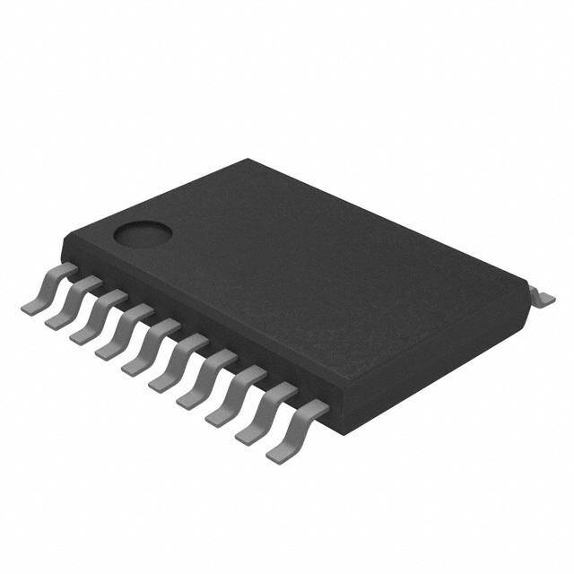
| 供应商器件封装 | 20-TSSOP |
| 其它名称 | 296-13087-1 |
| 功能 | Transceiver |
| 包装 | 剪切带 (CT) |
| 协议 | RS232 |
| 单位重量 | 77 mg |
| 双工 | 全 |
| 商标 | Texas Instruments |
| 安装类型 | 表面贴装 |
| 安装风格 | SMD/SMT |
| 封装 | Reel |
| 封装/外壳 | 20-TSSOP(0.173",4.40mm 宽) |
| 封装/箱体 | TSSOP-20 |
| 工作温度 | -40°C ~ 85°C |
| 工作温度范围 | - 40 C to + 85 C |
| 工作电源电压 | 3.3 V, 5 V |
| 工厂包装数量 | 2000 |
| 接收器滞后 | 300mV |
| 接收机数量 | 2 Receiver |
| 数据速率 | 250kbps |
| 最大工作温度 | + 85 C |
| 最小工作温度 | - 40 C |
| 标准包装 | 1 |
| 激励器数量 | 2 Driver |
| 电压-电源 | 3 V ~ 5.5 V |
| 电源电流 | 1 mA |
| 类型 | 收发器 |
| 系列 | MAX3222 |
| 驱动器/接收器数 | 2/2 |


- 商务部:美国ITC正式对集成电路等产品启动337调查
- 曝三星4nm工艺存在良率问题 高通将骁龙8 Gen1或转产台积电
- 太阳诱电将投资9.5亿元在常州建新厂生产MLCC 预计2023年完工
- 英特尔发布欧洲新工厂建设计划 深化IDM 2.0 战略
- 台积电先进制程称霸业界 有大客户加持明年业绩稳了
- 达到5530亿美元!SIA预计今年全球半导体销售额将创下新高
- 英特尔拟将自动驾驶子公司Mobileye上市 估值或超500亿美元
- 三星加码芯片和SET,合并消费电子和移动部门,撤换高东真等 CEO
- 三星电子宣布重大人事变动 还合并消费电子和移动部门
- 海关总署:前11个月进口集成电路产品价值2.52万亿元 增长14.8%


PDF Datasheet 数据手册内容提取
Product Sample & Technical Tools & Support & Folder Buy Documents Software Community MAX3222 SLLS408H–JANUARY2000–REVISEDOCTOBER2016 MAX3222 3-V to 5.5-V Multichannel RS-232 Line Driver and Receiver With ±15-kV ESD Protection 1 Features 3 Description • RS-232Bus-PinESDProtectionExceeds ±15kV The MAX3222 consists of two line drivers, two line 1 receivers,andadualcharge-pumpcircuitwith±15-kV UsingHuman-BodyModel(HBM) ESD protection pin to pin (serial-port connection pins, • MeetsorExceedstheRequirementsof including GND). The device meets the requirements TIA/EIA-232-FandITUv.28Standards of TIA/EIA-232-F and provides the electrical interface • OperatesWith3-Vto5.5-VV Supply between an asynchronous communication controller CC and the serial-port connector. The charge pump and • OperatesUpto250kbps four small external capacitors allow operation from a • TwoDriversandTwoReceivers single 3-V to 5.5-V supply. The device operates at • LowStandbyCurrent:1 µATypical data signaling rates up to 250 kbit/s and a maximum • ExternalCapacitors:4 ×0.1 µF of30-V/μsdriveroutputslewrate. • Accepts5-VLogicInputWith3.3-VSupply The MAX3222 can be placed in the power-down • AlternativeHigh-SpeedPin-CompatibleDevice mode by setting PWRDOWN low, which draws only 1 μA from the power supply. When the device is (1Mbps) powered down, the receivers remain active while the – SNx5C3222 drivers are placed in the high-impedance state. Receiver outputs also can be placed in the high- 2 Applications impedancestatebysetting ENhigh. • Battery-PoweredSystems DeviceInformation(1) • PDAs PARTNUMBER PACKAGE BODYSIZE(NOM) • Notebooks MAX3222CDW, • Laptops MAX322IDW SOIC(20) 12.80mm×7.50mm • PalmtopPCs MAX3222CDB, SSOP(20) 7.20mm×5.30mm MAX322IDB • Hand-heldEquipment MAX3222CPW, TSSOP(20) 6.50mm×4.40mm MAX322IPW (1) For all available packages, see the orderable addendum at theendofthedatasheet. BlockDiagram 13 17 DIN1 DOUT1 12 8 DIN2 DOUT2 20 PWRDOWN Powerdown 1 EN 15 16 ROUT1 RIN1 10 9 ROUT2 RIN2 1 An IMPORTANT NOTICE at the end of this data sheet addresses availability, warranty, changes, use in safety-critical applications, intellectualpropertymattersandotherimportantdisclaimers.PRODUCTIONDATA.
MAX3222 SLLS408H–JANUARY2000–REVISEDOCTOBER2016 www.ti.com Table of Contents 1 Features.................................................................. 1 8.1 Overview.................................................................10 2 Applications........................................................... 1 8.2 FunctionalBlockDiagram.......................................10 3 Description............................................................. 1 8.3 FeatureDescription.................................................11 8.4 DeviceFunctionalModes........................................11 4 RevisionHistory..................................................... 2 9 ApplicationandImplementation........................ 12 5 PinConfigurationandFunctions......................... 3 9.1 ApplicationInformation............................................12 6 Specifications......................................................... 4 9.2 TypicalApplication .................................................12 6.1 AbsoluteMaximumRatings......................................4 10 PowerSupplyRecommendations..................... 13 6.2 ESDRatings..............................................................4 11 Layout................................................................... 13 6.3 RecommendedOperatingConditions.......................4 6.4 ThermalInformation..................................................5 11.1 LayoutGuidelines.................................................13 6.5 ElectricalCharacteristics:Device..............................5 11.2 LayoutExample....................................................14 6.6 ElectricalCharacteristics:Driver...............................5 12 DeviceandDocumentationSupport................. 15 6.7 ElectricalCharacteristics:Receiver..........................6 12.1 ReceivingNotificationofDocumentationUpdates15 6.8 SwitchingCharacteristics:Driver..............................6 12.2 CommunityResources..........................................15 6.9 SwitchingCharacteristics:Receiver..........................6 12.3 Trademarks...........................................................15 6.10 TypicalCharacteristics............................................7 12.4 ElectrostaticDischargeCaution............................15 7 ParameterMeasurementInformation..................8 12.5 Glossary................................................................15 8 DetailedDescription............................................ 10 13 Mechanical,Packaging,andOrderable Information........................................................... 15 4 Revision History NOTE:Pagenumbersforpreviousrevisionsmaydifferfrompagenumbersinthecurrentversion. ChangesfromRevisionG(March2004)toRevisionH Page • AddedESDRatingstable,FeatureDescriptionsection,DeviceFunctionalModes,ApplicationandImplementation section,PowerSupplyRecommendationssection,Layoutsection,DeviceandDocumentationSupportsection,and Mechanical,Packaging,andOrderableInformationsection.................................................................................................. 1 • DeletedODERINGINFORMATIONtable;seePOAattheendofthedatasheet................................................................. 3 • ChangedR forDB,DWandPWpackagefrom:70°C/Wto84.4°C/W(DB),58°C/Wto70.2°C/W(DW)and83 θJA °C/Wto94.3°C/W(PW)intheThermalInformationtable.................................................................................................... 5 2 SubmitDocumentationFeedback Copyright©2000–2016,TexasInstrumentsIncorporated ProductFolderLinks:MAX3222
MAX3222 www.ti.com SLLS408H–JANUARY2000–REVISEDOCTOBER2016 5 Pin Configuration and Functions DB,DW,orPWPackage 20-PinSOIC,SSOP,TSSOP TopView EN 1 20 PWRDOWN C1+ 2 19 VCC V+ 3 18 GND C1− 4 17 DOUT1 C2+ 5 16 RIN1 C2− 6 15 ROUT1 V− 7 14 NC DOUT2 8 13 DIN1 RIN2 9 12 DIN2 ROUT2 10 11 NC NC−No internal connection PinFunctions PIN I/O DESCRIPTION NAME NO. C1+ 2 — Chargepumpcapacitorpin C1- 4 — Chargepumpcapacitorpin C2+ 5 — Chargepumpcapacitorpin C2- 6 — Chargepumpcapacitorpin DIN1 13 I Driverlogicinput DIN2 12 I Driverlogicinput DOUT1 17 O RS-232driveroutput DOUT2 8 O RS-232driveroutput EN 1 I Receiverenable,activelow GND 18 — Ground NC 11,14 — Nointernalconnection PWRDOWN 20 I Driverdisable,activelow RIN1 16 I RS-232receiverinput RIN2 9 I RS-232receiverinput ROUT1 15 O Receiverlogicoutput ROUT2 10 O Receiverlogicoutput V 19 — PowerSupply CC V+ 3 — Chargepumpcapacitorpin V- 7 — Chargepumpcapacitorpin Copyright©2000–2016,TexasInstrumentsIncorporated SubmitDocumentationFeedback 3 ProductFolderLinks:MAX3222
MAX3222 SLLS408H–JANUARY2000–REVISEDOCTOBER2016 www.ti.com 6 Specifications 6.1 Absolute Maximum Ratings overoperatingfree-airtemperaturerange(unlessotherwisenoted)(1) MIN MAX UNIT Supplyvoltage,V (2) –0.3 6 V CC Positiveoutputsupplyvoltage,V+(2) –0.3 7 V Negativeoutputsupplyvoltage,V–(2) 0.3 -7 V Supplyvoltagedifference,V+–V– 13 V Drivers,EN,PWRDOWN –0.3 6 Inputvoltage,V V I Receiver –25 25 Drivers –13.2 13.2 Outputvoltage,V V O Receivers –0.3 V +0.3 CC Operatingvirtualjunctiontemperature,T 150 °C J Storagetemperature,T –65 150 °C stg (1) StressesbeyondthoselistedunderAbsoluteMaximumRatingsmaycausepermanentdamagetothedevice.Thesearestressratings only,whichdonotimplyfunctionaloperationofthedeviceattheseoranyotherconditionsbeyondthoseindicatedunderRecommended OperatingConditions.Exposuretoabsolute-maximum-ratedconditionsforextendedperiodsmayaffectdevicereliability. (2) AllvoltagesarewithrespecttonetworkGND. 6.2 ESD Ratings VALUE UNIT Pins8,9,16,17 Human-bodymodel(HBM),perANSI/ESDA/JEDECJS-001 and18 ±15000 Electrostatic RIN,DOUT,andGNDpins (1) V Allotherpins ±3000 V (ESD) discharge Charged-devicemodel(CDM),perJEDECspecificationJESD22- C101(2) Allpins ±1500 (1) JEDECdocumentJEP155statesthat500-VHBMallowssafemanufacturingwithastandardESDcontrolprocess. (2) JEDECdocumentJEP157statesthat250-VCDMallowssafemanufacturingwithastandardESDcontrolprocess. 6.3 Recommended Operating Conditions overoperatingfree-airtemperaturerange(unlessotherwisenoted)(1).SeeFigure8. MIN NOM MAX UNIT V =3.3V 3 3.3 3.6 CC Supplyvoltage V V =5V 4.5 5 5.5 CC Driverandcontrolhigh-level VCC=3.3V 2 VIH DIR,EN,PWRDOWN V inputvoltage V =5V 2.4 CC Driverandcontrollow-level VIL DIR,EN,PWRDOWN 0.8 V inputvoltage VI Driverandcontrolinputvoltage DIR,EN,PWRDOWN 0 5.5 V VI Receiverinputvoltage –25 25 V MAX3222C 0 70 TA Operatingfree-airtemperature ºC MAX3222I –40 85 (1) TestconditionsareC1−C4=0.1μFatV =3.3V±0.3V;C1=0.047μF,C2−C4=0.33μFatV =5V±0.5V. CC CC 4 SubmitDocumentationFeedback Copyright©2000–2016,TexasInstrumentsIncorporated ProductFolderLinks:MAX3222
MAX3222 www.ti.com SLLS408H–JANUARY2000–REVISEDOCTOBER2016 6.4 Thermal Information MAX3222 THERMALMETRIC(1)(2)(3) DB(SSOP) DW(SOIC) PW(TSSOP) UNIT 20PINS 20PINS 20PINS R Junction-to-ambientthermalresistance 84.4 70.2 94.3 °C/W θJA R Junction-to-case(top)thermalresistance 44.1 36.2 29.9 °C/W θJC(top) R Junction-to-boardthermalresistance 40 37.9 45.1 °C/W θJB ψ Junction-to-topcharacterizationparameter 11 11.1 1.4 °C/W JT ψ Junction-to-boardcharacterizationparameter 39.5 37.5 44.6 °C/W JB (1) Formoreinformationabouttraditionalandnewthermalmetrics,seetheSemiconductorandICPackageThermalMetricsapplication report. (2) MaximumpowerdissipationisafunctionofT ,θ ,andT .Themaximumallowablepowerdissipationatanyallowableambient J(max) JA A temperatureisP =(T −T )/θ .OperatingattheabsolutemaximumT of150°Ccanaffectreliability. D J(max) A JA J (3) ThepackagethermalimpedanceiscalculatedinaccordancewithJESD51-7. 6.5 Electrical Characteristics: Device overoperatingfree-airtemperaturerange(unlessotherwisenoted)(1).SeeFigure8. PARAMETER TESTCONDITIONS MIN TYP(2) MAX UNIT Inputleakagecurrent(EN, II ±0.01 ±1 µA PWRDOWN) Supplycurrent Noload,PWRDOWNatV 0.3 1 mA CC I CC Supplycurrent(poweredoff) Noload,PWRDOWNatGND 1 10 µA (1) TestconditionsareC1−C4=0.1μFatV =3.3V±0.3V;C1=0.047μF,C2−C4=0.33μFatV =5V±0.5V. CC CC (2) AlltypicalvaluesareatV =3.3VorV =5V,andT =25°C. CC CC A 6.6 Electrical Characteristics: Driver overoperatingfree-airtemperaturerange(unlessotherwisenoted)(1).SeeFigure8. PARAMETER TESTCONDITIONS MIN TYP(2) MAX UNIT DOUTatR =3kΩtoGND,DIN= V High-leveloutputvoltage L 5 5.4 V OH GND DOUTatR =3kΩtoGND,DIN= V Low-leveloutputvoltage L –5 –5.4 V OL V CC I High-levelinputcurrent V =V ±0.01 ±1 µA IH I CC I Low-levelinputcurrent V atGND ±0.01 ±1 µA IL I V =3.6V,V =0V CC O I Short-circuitoutputcurrent ±35 ±60 mA OS V =5.5V,V =0V CC O r Outputresistance V ,V+,andV–=0V,V =±2V 300 10M Ω o CC O PWRDOWN=GND,V =±12V, O ±25 V =3Vto3.6V CC I Outputleakagecurrent µA off PWRDOWN=GND,V =±10V, O ±25 V =4.5Vto5.5V CC (1) TestconditionsareC1−C4=0.1μFatV =3.3V±0.3V;C1=0.047μF,C2−C4=0.33μFatV =5V±0.5V. CC CC (2) AlltypicalvaluesareatV =3.3VorV =5V,andT =25°C. CC CC A Copyright©2000–2016,TexasInstrumentsIncorporated SubmitDocumentationFeedback 5 ProductFolderLinks:MAX3222
MAX3222 SLLS408H–JANUARY2000–REVISEDOCTOBER2016 www.ti.com 6.7 Electrical Characteristics: Receiver overoperatingfree-airtemperaturerange(unlessotherwisenoted)(1).SeeFigure8. PARAMETER TESTCONDITIONS MIN TYP(2) MAX UNIT V High-leveloutputvoltage I =–1mA V –0.6 V –0.1 V OH OH CC CC V Low-leveloutputvoltage I =1.6mA 0.4 V OL OL Positive-goinginputthreshold VCC=3.3V 1.5 2.4 V V IT+ voltage V =5V 1.8 2.4 CC Negative-goinginputthreshold VCC=3.3V 0.6 1.2 V V IT– voltage V =5V 0.8 1.5 CC V Inputhysteresis(V –V ) 0.3 V hys IT+ IT– I Outputleakagecurrent EN=V ±0.05 ±10 µA off CC r Inputresistance V =±3Vto±25V 3 5 7 kΩ i I (1) TestconditionsareC1−C4=0.1μFatV =3.3V±0.3V;C1=0.047μF,C2−C4=0.33μFatV =5V±0.5V. CC CC (2) AlltypicalvaluesareatV =3.3VorV =5V,andT =25°C. CC CC A 6.8 Switching Characteristics: Driver overoperatingfree-airtemperaturerange(unlessotherwisenoted)(1).SeeFigure8. PARAMETER TESTCONDITIONS MIN TYP(2) MAX UNIT C =1000pF,R =3kΩ,OneDOUTswitching,see Maximumdatarate L L 150 250 kbps Figure3 t Pulseskew(3) CL=150pFto2500pF,RL=3kΩto7kΩ,see 300 ns sk(p) Figure4 C =150pFto1000 L 6 30 Slewrate,transitionregion R =3kΩto7kΩ,V =3.3 pF SR(tr) L CC V/µs (seeFigure3) V C =150pFto2500 L 4 30 pF (1) TestconditionsareC1−C4=0.1μFatV =3.3V±0.3V;C1=0.047μF,C2−C4=0.33μFatV =5V±0.5V. CC CC (2) AlltypicalvaluesareatV =3.3VorV =5V,andT =25°C. CC CC A (3) Pulseskewisdefinedas|tPLH−tPHL|ofeachchannelofthesamedevice. 6.9 Switching Characteristics: Receiver overoperatingfree-airtemperaturerange(unlessotherwisenoted)(1).SeeFigure8. PARAMETER TESTCONDITIONS MIN TYP(2) MAX UNIT Propagationdelaytime,low-tohigh- t C =150pF,seeFigure5 300 ns PLH leveloutput L Propagationdelaytime,high-tolow- t C =150pF,seeFigure5 300 ns PHL leveloutput L C =150pF,R =3kΩ,see t Outputenabletime L L 200 ns en Figure6 C =150pF,R =3kΩ,see t Outputdisabletime L L 200 ns dis Figure6 t Pulseskew(3) SeeFigure5 300 ns sk(p) (1) TestconditionsareC1−C4=0.1μFatV =3.3V±0.3V;C1=0.047μF,C2−C4=0.33μFatV =5V±0.5V. CC CC (2) AlltypicalvaluesareatV =3.3VorV =5V,andT =25°C. CC CC A (3) Pulseskewisdefinedas|tPLH−tPHL|ofeachchannelofthesamedevice. 6 SubmitDocumentationFeedback Copyright©2000–2016,TexasInstrumentsIncorporated ProductFolderLinks:MAX3222
MAX3222 www.ti.com SLLS408H–JANUARY2000–REVISEDOCTOBER2016 6.10 Typical Characteristics T =25°C;V =3.3V A CC 6 0 5 -1 4 -2 V) V) UT ( 3 UT ( -3 O O D D 2 -4 1 -5 0 -6 0 2 4 6 8 10 12 14 16 18 20 0 2 4 6 8 10 12 14 16 18 20 DOUT VOH vs. DOUT Current DOUT VOL vs. DOUT Current D001 D002 Figure1.DriverVOHvsLoadCurrent Figure2.DriverVOLvsLoadCurrent Copyright©2000–2016,TexasInstrumentsIncorporated SubmitDocumentationFeedback 7 ProductFolderLinks:MAX3222
MAX3222 SLLS408H–JANUARY2000–REVISEDOCTOBER2016 www.ti.com 7 Parameter Measurement Information 3 V Input 1.5 V 1.5 V RS-232 0 V Generator Output (see Note B) 50Ω CL RL (see NoteA) tTHL tTLH 3 V VOH PWRDOWN Output 3 V 3 V −3 V −3 V VOL TEST CIRCUIT VOLTAGEWAVEFORMS 6V SR(tr) t ort THL TLH NOTES: A. CLincludes probe and jig capacitance. B. The pulse generator has the following characteristics: PRR = 250 kbit/s, ZO= 50Ω, 50% duty cycle, tr≤10 ns, tf≤10 ns. Figure3. DriverSlewRate 3 V RS-232 Input 1.5V 1.5 V Output 0 V Generator 50Ω (see Note B) CL tPHL tPLH RL (see NoteA) VOH 3 V Output 50% 50% PWRDOWN VOL TESTCIRCUIT VOLTAGEWAVEFORMS NOTES: A. CLincludes probe and jig capacitance. B. Thepulsegeneratorhasthefollowingcharacteristics:PRR=250kbit/s,ZO= 50Ω, 50% duty cycle, tr≤10 ns, tf≤10 ns. Figure4. DriverPulseSkew EN 3 V 0 V Input 1.5 V 1.5 V −3 V Output Generator (see Note B) 50Ω tPHL tPLH CL (see NoteA) VOH Output 50% 50% VOL TESTCIRCUIT VOLTAGEWAVEFORMS NOTES: A. CLincludes probe and jig capacitance. B. Thepulsegeneratorhasthefollowingcharacteristics:ZO= 50Ω, 50% duty cycle, tr≤10 ns, tf≤10 ns. Figure5. ReceiverPropagationDelayTimes 8 SubmitDocumentationFeedback Copyright©2000–2016,TexasInstrumentsIncorporated ProductFolderLinks:MAX3222
MAX3222 www.ti.com SLLS408H–JANUARY2000–REVISEDOCTOBER2016 Parameter Measurement Information (continued) VCC GND 3 V Input 1.5V 1.5V S1 0 V RL tPHZ tPZH 3 V or 0 V Output S1atGND) (S1atGND) VOH CL Output 50% EN (see NoteA) 0.3 V tPLZ Generator 50Ω (S1 at VCC) (see Note B) 0.3 V Output 50% VOL tPZL TESTCIRCUIT (S1 at VCC) VOLTAGEWAVEFORMS NOTES: A. CLincludes probe and jig capacitance. B. Thepulsegeneratorhasthefollowingcharacteristics:ZO= 50Ω, 50% duty cycle, tr≤10 ns, tf≤10 ns. Figure6. ReceiverEnableandDisableTimes Copyright©2000–2016,TexasInstrumentsIncorporated SubmitDocumentationFeedback 9 ProductFolderLinks:MAX3222
MAX3222 SLLS408H–JANUARY2000–REVISEDOCTOBER2016 www.ti.com 8 Detailed Description 8.1 Overview The MAX3222 consists of two line drivers, two line receivers, and a dual charge-pump circuit with ±15-kV ESD protection pin to pin (serial-port connection pins, including GND). The device meets the requirements of TIA/EIA- 232-F and provides the electrical interface between an asynchronous communication controller and the serial- port connector. The charge pump and four small external capacitors allow operation from a single 3-V to 5.5-V supply.Thedeviceoperatesatdatasignalingratesupto250kbit/sandamaximumof30-V/μsdriveroutputslew rate. The MAX3222 can be placed in the power-down mode by setting PWRDOWN low, which draws only 1 μA from the power supply. When the device is powered down, the receivers remain active while the drivers are placed in the high-impedance state. Also, during power down, the onboard charge pump is disabled; V+ is lowered to V , CC and V− is raised toward GND. Receiver outputs also can be placed in the high-impedance state by setting EN high. 8.2 Functional Block Diagram DIN1 13 17 DOUT1 DIN2 12 8 DOUT2 PWRDOWN 20 Powerdown EN 1 ROUT1 15 16 RIN1 ROUT2 10 9 RIN2 Figure7. LogicDiagram(PositiveLogic) 10 SubmitDocumentationFeedback Copyright©2000–2016,TexasInstrumentsIncorporated ProductFolderLinks:MAX3222
MAX3222 www.ti.com SLLS408H–JANUARY2000–REVISEDOCTOBER2016 8.3 Feature Description 8.3.1 Power The power block increases, inverts, and regulates voltage at V+ and V- pins using a charge pump that requires fourexternalcapacitors. 8.3.2 RS232Driver Two drivers interface standard logic level to RS232 levels. PWRDOWN input low turns driver off and PWRDOWN input high turns driver on. Both DIN inputs and PWRDOWN input must be valid high or low. Do not floatlogicinputpins. 8.3.3 RS232Receiver TworeceiversinterfaceRS232levelstostandardlogiclevels.AnopeninputwillresultinahighoutputonROUT. Each RIN input includes an internal standard RS232 load. EN input low turns on both ROUT pins. EN input high puts both ROUT pins into high impedance state, output off. EN input must be valid high or low. Do not float logic inputpins. 8.4 Device Functional Modes Driverandreceiveroutputsarecontrolledbythefunctionaltruthtables. Table1.FunctionalTable-EachDriver(1) INPUTS OUTPUTDOUT DIN PWRDOWN X L Z L H H H H L (1) H=highlevel,L=lowlevel,X=irrelevant,Z=highimpedance Table2.FunctionalTable-EachReceiver(1) INPUTS OUTPUTROUT RIN EN L L H H L L X H Z Open L H (1) H=highlevel,L=lowlevel,X=irrelevant,Z=highimpedance(off),Open=inputdisconnectedor connecteddriveroff Copyright©2000–2016,TexasInstrumentsIncorporated SubmitDocumentationFeedback 11 ProductFolderLinks:MAX3222
MAX3222 SLLS408H–JANUARY2000–REVISEDOCTOBER2016 www.ti.com 9 Application and Implementation NOTE Information in the following applications sections is not part of the TI component specification, and TI does not warrant its accuracy or completeness. TI’s customers are responsible for determining suitability of components for their purposes. Customers should validateandtesttheirdesignimplementationtoconfirmsystemfunctionality. 9.1 Application Information The MAX3222 interfaces a universal asynchronous receiver / transmitter (UART) to RS-232 port voltage levels. External capacitors are used to generate RS-232 compliant voltages. For proper operation, add capacitors as showninFigure8. 9.2 Typical Application ROUT and DIN connect to UART or general purpose logic lines. RIN and DOUT lines connect to a RS232 connectororcable. EN 1 Powerdown 20 PWRDOWN 2 C1+ VCC 19 + CBYPASS + 3 18 − = 0.1µF C1− C3+ V+ GND − 4 17 C1− DOUT1 5 16 C2+ RIN1 + C2 − 6 15 C2− ROUT1 7 14 − V− NC C4 + 8 13 DOUT2 DIN1 RIN2 9 12 DIN2 ROUT2 10 11 NC C3canbeconnectedtoV orGND. CC Resistorvaluesshownarenominal. NC−Nointernalconnection Nonpolarizedceramiccapacitorsareacceptable.Ifpolarizedtantalumorelectrolyticcapacitorsareused,theyshould beconnectedasshown. Figure8. RecommendedApplicationSchematic 9.2.1 DesignRequirements • RecommendedV is3.3Vor5V.3Vto5.5Visalsopossible CC • Maximumrecommendedbitrateis250kbit/s. Table3.V vsCapacitorValues CC VCC C1 C2,C3,andC4 3.3V±0.3V 0.1µF 0.1µF 5V±0.5V 0.047µF 0.33µF 3V±5.5V 0.1µF 0.47µF 12 SubmitDocumentationFeedback Copyright©2000–2016,TexasInstrumentsIncorporated ProductFolderLinks:MAX3222
MAX3222 www.ti.com SLLS408H–JANUARY2000–REVISEDOCTOBER2016 9.2.2 DetailedDesignProcedure • AllDIN, PWRDOWNandENinputsmustbeconnectedtovalidloworhighlogiclevels. • SelectcapacitorvaluesbasedonVCClevelforbestperformance. 9.2.3 ApplicationCurves 8 8 6 6 4 4 e (V) 2 e (V) 2 g g a a olt 0 olt 0 V V -2 -2 DIN DIN -4 -4 DOUT DOUT ROUT ROUT -6 -6 0 1 2 3 4 5 6 7 8 9 10 0 1 2 3 4 5 6 7 8 9 10 Time (us) Time (us) D004 D003 Figure9.LoopbackWaveforms Figure10.LoopbackWaveformswith1-nFload V =3.3V,DataRate250kbit/s V =3.3V,DataRate250kbit/s CC CC 10 Power Supply Recommendations V shouldbebetween3Vand5.5V.ChargepumpcapacitorsshouldbechosenusingtableinTable3. CC 11 Layout 11.1 Layout Guidelines Keep the external capacitor traces short. This is more important on C1 and C2 nodes that have the fastest rise and fall times. Make the impedance from MAX3222 ground pin and circuit board's ground plane as low as possibleforbestESDperformance.Usewidemetalandmultipleviasonbothsidesofgroundpin Copyright©2000–2016,TexasInstrumentsIncorporated SubmitDocumentationFeedback 13 ProductFolderLinks:MAX3222
MAX3222 SLLS408H–JANUARY2000–REVISEDOCTOBER2016 www.ti.com 11.2 Layout Example 1 EN PWRDOWN 20 Ground C3 2 C1+ VCC 19 VCC (cid:19)(cid:17)(cid:20)PF C1 3 V+ GND 18 Ground 4 C1- DOUT1 17 5 C2+ RIN1 16 C2 6 C2- ROUT1 15 Ground 7 V- NC 14 C4 8 DOUT2 DIN1 13 9 RIN2 DIN2 12 10 ROUT2 NC 11 Figure11. MAX3222Layout 14 SubmitDocumentationFeedback Copyright©2000–2016,TexasInstrumentsIncorporated ProductFolderLinks:MAX3222
MAX3222 www.ti.com SLLS408H–JANUARY2000–REVISEDOCTOBER2016 12 Device and Documentation Support 12.1 Receiving Notification of Documentation Updates To receive notification of documentation updates, navigate to the device product folder on ti.com. In the upper right corner, click on Alert me to register and receive a weekly digest of any product information that has changed.Forchangedetails,reviewtherevisionhistoryincludedinanyreviseddocument. 12.2 Community Resources The following links connect to TI community resources. Linked contents are provided "AS IS" by the respective contributors. They do not constitute TI specifications and do not necessarily reflect TI's views; see TI's Terms of Use. TIE2E™OnlineCommunity TI'sEngineer-to-Engineer(E2E)Community.Createdtofostercollaboration amongengineers.Ate2e.ti.com,youcanaskquestions,shareknowledge,exploreideasandhelp solveproblemswithfellowengineers. DesignSupport TI'sDesignSupport QuicklyfindhelpfulE2Eforumsalongwithdesignsupporttoolsand contactinformationfortechnicalsupport. 12.3 Trademarks E2EisatrademarkofTexasInstruments. Allothertrademarksarethepropertyoftheirrespectiveowners. 12.4 Electrostatic Discharge Caution Thesedeviceshavelimitedbuilt-inESDprotection.Theleadsshouldbeshortedtogetherorthedeviceplacedinconductivefoam duringstorageorhandlingtopreventelectrostaticdamagetotheMOSgates. 12.5 Glossary SLYZ022—TIGlossary. Thisglossarylistsandexplainsterms,acronyms,anddefinitions. 13 Mechanical, Packaging, and Orderable Information The following pages include mechanical, packaging, and orderable information. This information is the most current data available for the designated devices. This data is subject to change without notice and revision of thisdocument.Forbrowser-basedversionsofthisdatasheet,refertotheleft-handnavigation. Copyright©2000–2016,TexasInstrumentsIncorporated SubmitDocumentationFeedback 15 ProductFolderLinks:MAX3222
PACKAGE OPTION ADDENDUM www.ti.com 6-Feb-2020 PACKAGING INFORMATION Orderable Device Status Package Type Package Pins Package Eco Plan Lead/Ball Finish MSL Peak Temp Op Temp (°C) Device Marking Samples (1) Drawing Qty (2) (6) (3) (4/5) MAX3222CDB ACTIVE SSOP DB 20 70 Green (RoHS NIPDAU Level-1-260C-UNLIM 0 to 70 MA3222C & no Sb/Br) MAX3222CDBR ACTIVE SSOP DB 20 2000 Green (RoHS NIPDAU Level-1-260C-UNLIM 0 to 70 MA3222C & no Sb/Br) MAX3222CDBRE4 ACTIVE SSOP DB 20 2000 Green (RoHS NIPDAU Level-1-260C-UNLIM 0 to 70 MA3222C & no Sb/Br) MAX3222CDBRG4 ACTIVE SSOP DB 20 2000 Green (RoHS NIPDAU Level-1-260C-UNLIM 0 to 70 MA3222C & no Sb/Br) MAX3222CDW ACTIVE SOIC DW 20 25 Green (RoHS NIPDAU Level-1-260C-UNLIM 0 to 70 MAX3222C & no Sb/Br) MAX3222CDWR ACTIVE SOIC DW 20 2000 Green (RoHS NIPDAU Level-1-260C-UNLIM 0 to 70 MAX3222C & no Sb/Br) MAX3222CDWRE4 ACTIVE SOIC DW 20 2000 Green (RoHS NIPDAU Level-1-260C-UNLIM 0 to 70 MAX3222C & no Sb/Br) MAX3222CPW ACTIVE TSSOP PW 20 70 Green (RoHS NIPDAU Level-1-260C-UNLIM 0 to 70 MA3222C & no Sb/Br) MAX3222CPWR ACTIVE TSSOP PW 20 2000 Green (RoHS NIPDAU Level-1-260C-UNLIM 0 to 70 MA3222C & no Sb/Br) MAX3222IDB ACTIVE SSOP DB 20 70 Green (RoHS NIPDAU Level-1-260C-UNLIM -40 to 85 MB3222I & no Sb/Br) MAX3222IDBR ACTIVE SSOP DB 20 2000 Green (RoHS NIPDAU Level-1-260C-UNLIM -40 to 85 MB3222I & no Sb/Br) MAX3222IDBRE4 ACTIVE SSOP DB 20 2000 Green (RoHS NIPDAU Level-1-260C-UNLIM -40 to 85 MB3222I & no Sb/Br) MAX3222IDW ACTIVE SOIC DW 20 25 Green (RoHS NIPDAU Level-1-260C-UNLIM -40 to 85 MAX3222I & no Sb/Br) MAX3222IDWG4 ACTIVE SOIC DW 20 25 Green (RoHS NIPDAU Level-1-260C-UNLIM -40 to 85 MAX3222I & no Sb/Br) MAX3222IDWR ACTIVE SOIC DW 20 2000 Green (RoHS NIPDAU Level-1-260C-UNLIM -40 to 85 MAX3222I & no Sb/Br) MAX3222IPW ACTIVE TSSOP PW 20 70 Green (RoHS NIPDAU Level-1-260C-UNLIM -40 to 85 MB3222I & no Sb/Br) MAX3222IPWR ACTIVE TSSOP PW 20 2000 Green (RoHS NIPDAU Level-1-260C-UNLIM -40 to 85 MB3222I & no Sb/Br) Addendum-Page 1
PACKAGE OPTION ADDENDUM www.ti.com 6-Feb-2020 Orderable Device Status Package Type Package Pins Package Eco Plan Lead/Ball Finish MSL Peak Temp Op Temp (°C) Device Marking Samples (1) Drawing Qty (2) (6) (3) (4/5) MAX3222IPWRE4 ACTIVE TSSOP PW 20 2000 Green (RoHS NIPDAU Level-1-260C-UNLIM -40 to 85 MB3222I & no Sb/Br) (1) The marketing status values are defined as follows: ACTIVE: Product device recommended for new designs. LIFEBUY: TI has announced that the device will be discontinued, and a lifetime-buy period is in effect. NRND: Not recommended for new designs. Device is in production to support existing customers, but TI does not recommend using this part in a new design. PREVIEW: Device has been announced but is not in production. Samples may or may not be available. OBSOLETE: TI has discontinued the production of the device. (2) RoHS: TI defines "RoHS" to mean semiconductor products that are compliant with the current EU RoHS requirements for all 10 RoHS substances, including the requirement that RoHS substance do not exceed 0.1% by weight in homogeneous materials. Where designed to be soldered at high temperatures, "RoHS" products are suitable for use in specified lead-free processes. TI may reference these types of products as "Pb-Free". RoHS Exempt: TI defines "RoHS Exempt" to mean products that contain lead but are compliant with EU RoHS pursuant to a specific EU RoHS exemption. Green: TI defines "Green" to mean the content of Chlorine (Cl) and Bromine (Br) based flame retardants meet JS709B low halogen requirements of <=1000ppm threshold. Antimony trioxide based flame retardants must also meet the <=1000ppm threshold requirement. (3) MSL, Peak Temp. - The Moisture Sensitivity Level rating according to the JEDEC industry standard classifications, and peak solder temperature. (4) There may be additional marking, which relates to the logo, the lot trace code information, or the environmental category on the device. (5) Multiple Device Markings will be inside parentheses. Only one Device Marking contained in parentheses and separated by a "~" will appear on a device. If a line is indented then it is a continuation of the previous line and the two combined represent the entire Device Marking for that device. (6) Lead/Ball Finish - Orderable Devices may have multiple material finish options. Finish options are separated by a vertical ruled line. Lead/Ball Finish values may wrap to two lines if the finish value exceeds the maximum column width. Important Information and Disclaimer:The information provided on this page represents TI's knowledge and belief as of the date that it is provided. TI bases its knowledge and belief on information provided by third parties, and makes no representation or warranty as to the accuracy of such information. Efforts are underway to better integrate information from third parties. TI has taken and continues to take reasonable steps to provide representative and accurate information but may not have conducted destructive testing or chemical analysis on incoming materials and chemicals. TI and TI suppliers consider certain information to be proprietary, and thus CAS numbers and other limited information may not be available for release. In no event shall TI's liability arising out of such information exceed the total purchase price of the TI part(s) at issue in this document sold by TI to Customer on an annual basis. Addendum-Page 2
PACKAGE MATERIALS INFORMATION www.ti.com 2-Oct-2019 TAPE AND REEL INFORMATION *Alldimensionsarenominal Device Package Package Pins SPQ Reel Reel A0 B0 K0 P1 W Pin1 Type Drawing Diameter Width (mm) (mm) (mm) (mm) (mm) Quadrant (mm) W1(mm) MAX3222CDBR SSOP DB 20 2000 330.0 16.4 8.2 7.5 2.5 12.0 16.0 Q1 MAX3222CDWR SOIC DW 20 2000 330.0 24.4 10.8 13.3 2.7 12.0 24.0 Q1 MAX3222CPWR TSSOP PW 20 2000 330.0 16.4 6.95 7.1 1.6 8.0 16.0 Q1 MAX3222IDBR SSOP DB 20 2000 330.0 16.4 8.2 7.5 2.5 12.0 16.0 Q1 MAX3222IDWR SOIC DW 20 2000 330.0 24.4 10.8 13.3 2.7 12.0 24.0 Q1 MAX3222IPWR TSSOP PW 20 2000 330.0 16.4 6.95 7.0 1.4 8.0 16.0 Q1 PackMaterials-Page1
PACKAGE MATERIALS INFORMATION www.ti.com 2-Oct-2019 *Alldimensionsarenominal Device PackageType PackageDrawing Pins SPQ Length(mm) Width(mm) Height(mm) MAX3222CDBR SSOP DB 20 2000 367.0 367.0 38.0 MAX3222CDWR SOIC DW 20 2000 367.0 367.0 45.0 MAX3222CPWR TSSOP PW 20 2000 367.0 367.0 38.0 MAX3222IDBR SSOP DB 20 2000 367.0 367.0 38.0 MAX3222IDWR SOIC DW 20 2000 367.0 367.0 45.0 MAX3222IPWR TSSOP PW 20 2000 367.0 367.0 38.0 PackMaterials-Page2
PACKAGE OUTLINE DB0020A SSOP - 2 mm max height SCALE 2.000 SMALL OUTLINE PACKAGE C 8.2 TYP 7.4 A 0.1 C PIN 1 INDEX AREA SEATING PLANE 18X 0.65 20 1 2X 7.5 5.85 6.9 NOTE 3 10 11 0.38 20X 0.22 5.6 B 0.1 C A B 5.0 NOTE 4 2 MAX (0.15) TYP 0.25 SEE DETAIL A GAGE PLANE 0 -8 0.95 0.05 MIN 0.55 DETA 15AIL A TYPICAL 4214851/B 08/2019 NOTES: 1. All linear dimensions are in millimeters. Any dimensions in parenthesis are for reference only. Dimensioning and tolerancing per ASME Y14.5M. 2. This drawing is subject to change without notice. 3. This dimension does not include mold flash, protrusions, or gate burrs. Mold flash, protrusions, or gate burrs shall not exceed 0.15 mm per side. 4. This dimension does not include interlead flash. Interlead flash shall not exceed 0.25 mm per side. 5. Reference JEDEC registration MO-150. www.ti.com
EXAMPLE BOARD LAYOUT DB0020A SSOP - 2 mm max height SMALL OUTLINE PACKAGE 20X (1.85) SYMM (R0.05) TYP 1 20X (0.45) 20 SYMM 18X (0.65) 10 11 (7) LAND PATTERN EXAMPLE EXPOSED METAL SHOWN SCALE: 10X SOLDER MASK METAL METAL UNDER SOLDER MASK OPENING SOLDER MASK OPENING EXPOSED METAL EXPOSED METAL 0.07 MAX 0.07 MIN ALL AROUND ALL AROUND NON-SOLDER MASK SOLDER MASK DEFINED DEFINED (PREFERRED) SOLDE15.000 R MASK DETAILS 4214851/B 08/2019 NOTES: (continued) 6. Publication IPC-7351 may have alternate designs. 7. Solder mask tolerances between and around signal pads can vary based on board fabrication site. www.ti.com
EXAMPLE STENCIL DESIGN DB0020A SSOP - 2 mm max height SMALL OUTLINE PACKAGE 20X (1.85) SYMM (R0.05) TYP 1 20X (0.45) 20 SYMM 18X (0.65) 10 11 (7) SOLDER PASTE EXAMPLE BASED ON 0.125 mm THICK STENCIL SCALE: 10X 4214851/B 08/2019 NOTES: (continued) 8. Laser cutting apertures with trapezoidal walls and rounded corners may offer better paste release. IPC-7525 may have alternate design recommendations. 9. Board assembly site may have different recommendations for stencil design. www.ti.com
None
None
PACKAGE OUTLINE DW0020A SOIC - 2.65 mm max height SCALE 1.200 SOIC C 10.63 SEATING PLANE TYP 9.97 A PIN 1 ID 0.1 C AREA 18X 1.27 20 1 13.0 2X 12.6 11.43 NOTE 3 10 11 0.51 20X 7.6 0.31 2.65 MAX B 7.4 0.25 C A B NOTE 4 0.33 TYP 0.10 0.25 SEE DETAIL A GAGE PLANE 0.3 1.27 0 - 8 0.1 0.40 DETAIL A TYPICAL 4220724/A 05/2016 NOTES: 1. All linear dimensions are in millimeters. Dimensions in parenthesis are for reference only. Dimensioning and tolerancing per ASME Y14.5M. 2. This drawing is subject to change without notice. 3. This dimension does not include mold flash, protrusions, or gate burrs. Mold flash, protrusions, or gate burrs shall not exceed 0.15 mm per side. 4. This dimension does not include interlead flash. Interlead flash shall not exceed 0.43 mm per side. 5. Reference JEDEC registration MS-013. www.ti.com
EXAMPLE BOARD LAYOUT DW0020A SOIC - 2.65 mm max height SOIC 20X (2) SYMM 1 20 20X (0.6) 18X (1.27) SYMM (R0.05) TYP 10 11 (9.3) LAND PATTERN EXAMPLE SCALE:6X SOOPLEDNEINRG MASK METAL MSOELTDAEL RU NMDAESRK SOOPLEDNEINRG MASK 0.07 MAX 0.07 MIN ALL AROUND ALL AROUND NON SOLDER MASK SOLDER MASK DEFINED DEFINED SOLDER MASK DETAILS 4220724/A 05/2016 NOTES: (continued) 6. Publication IPC-7351 may have alternate designs. 7. Solder mask tolerances between and around signal pads can vary based on board fabrication site. www.ti.com
EXAMPLE STENCIL DESIGN DW0020A SOIC - 2.65 mm max height SOIC 20X (2) SYMM 1 20 20X (0.6) 18X (1.27) SYMM 10 11 (9.3) SOLDER PASTE EXAMPLE BASED ON 0.125 mm THICK STENCIL SCALE:6X 4220724/A 05/2016 NOTES: (continued) 8. Laser cutting apertures with trapezoidal walls and rounded corners may offer better paste release. IPC-7525 may have alternate design recommendations. 9. Board assembly site may have different recommendations for stencil design. www.ti.com
IMPORTANTNOTICEANDDISCLAIMER TI PROVIDES TECHNICAL AND RELIABILITY DATA (INCLUDING DATASHEETS), DESIGN RESOURCES (INCLUDING REFERENCE DESIGNS), APPLICATION OR OTHER DESIGN ADVICE, WEB TOOLS, SAFETY INFORMATION, AND OTHER RESOURCES “AS IS” AND WITH ALL FAULTS, AND DISCLAIMS ALL WARRANTIES, EXPRESS AND IMPLIED, INCLUDING WITHOUT LIMITATION ANY IMPLIED WARRANTIES OF MERCHANTABILITY, FITNESS FOR A PARTICULAR PURPOSE OR NON-INFRINGEMENT OF THIRD PARTY INTELLECTUAL PROPERTY RIGHTS. These resources are intended for skilled developers designing with TI products. You are solely responsible for (1) selecting the appropriate TI products for your application, (2) designing, validating and testing your application, and (3) ensuring your application meets applicable standards, and any other safety, security, or other requirements. These resources are subject to change without notice. TI grants you permission to use these resources only for development of an application that uses the TI products described in the resource. Other reproduction and display of these resources is prohibited. No license is granted to any other TI intellectual property right or to any third party intellectual property right. TI disclaims responsibility for, and you will fully indemnify TI and its representatives against, any claims, damages, costs, losses, and liabilities arising out of your use of these resources. TI’s products are provided subject to TI’s Terms of Sale (www.ti.com/legal/termsofsale.html) or other applicable terms available either on ti.com or provided in conjunction with such TI products. TI’s provision of these resources does not expand or otherwise alter TI’s applicable warranties or warranty disclaimers for TI products. Mailing Address: Texas Instruments, Post Office Box 655303, Dallas, Texas 75265 Copyright © 2020, Texas Instruments Incorporated