ICGOO在线商城 > 集成电路(IC) > 数据采集 - 模数转换器 > AD7942BRMZ
 Datasheet下载
- 型号: AD7942BRMZ
- 制造商: Analog
- 库位|库存: xxxx|xxxx
- 要求:
| 数量阶梯 | 香港交货 | 国内含税 |
| +xxxx | $xxxx | ¥xxxx |
查看当月历史价格
查看今年历史价格
AD7942BRMZ产品简介:
ICGOO电子元器件商城为您提供AD7942BRMZ由Analog设计生产,在icgoo商城现货销售,并且可以通过原厂、代理商等渠道进行代购。 AD7942BRMZ价格参考¥92.67-¥92.67。AnalogAD7942BRMZ封装/规格:数据采集 - 模数转换器, 14 Bit Analog to Digital Converter 1 Input 1 SAR 10-MSOP。您可以下载AD7942BRMZ参考资料、Datasheet数据手册功能说明书,资料中有AD7942BRMZ 详细功能的应用电路图电压和使用方法及教程。
AD7942BRMZ是Analog Devices Inc.生产的一款14位、高速、低功耗的模数转换器(ADC),广泛应用于需要高精度和快速数据采集的场景。其主要应用场景包括:

1. 工业自动化与控制系统:用于传感器信号采集,如温度、压力、流量等模拟信号的数字化处理,适用于PLC(可编程逻辑控制器)和工业监测系统。

2. 通信设备:在无线基站、光纤通信等系统中用于射频或中频信号的数字化处理,支持高精度信号分析与传输。

3. 测试与测量仪器:如示波器、频谱分析仪、数据记录仪等,用于高精度信号采集与分析,满足实验室和现场测试需求。

4. 医疗电子设备:用于医疗成像设备(如超声波、CT)或生命体征监测设备中的信号采集,确保数据的高分辨率和稳定性。

5. 电力监测系统:用于智能电网、电能质量分析仪中,对电压、电流等信号进行实时采集与分析,支持电力系统的监控与故障诊断。

6. 航空航天与国防:适用于雷达、导航系统等对精度与稳定性要求极高的场合。

AD7942BRMZ具有80MSPS的采样率、低功耗设计和小封装,适合对空间和功耗有要求的便携式或高密度系统设计。
| 参数 | 数值 |
| 产品目录 | 集成电路 (IC)半导体 |
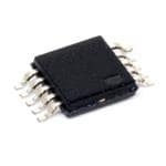
| 描述 | IC ADC 14BIT SRL 250KSPS 10MSOP模数转换器 - ADC 14-Bit 250KSPS PSEUDO DIFF IC |
| 产品分类 | |
| 品牌 | Analog Devices |
| 产品手册 | |
| 产品图片 |
|
| rohs | 符合RoHS无铅 / 符合限制有害物质指令(RoHS)规范要求 |
| 产品系列 | 数据转换器IC,模数转换器 - ADC,Analog Devices AD7942BRMZPulSAR® |
| 数据手册 | |
| 产品型号 | AD7942BRMZ |
| 产品目录页面 | |
| 产品种类 | 模数转换器 - ADC |
| 位数 | 14 |
| 供应商器件封装 | 10-MSOP |
| 信噪比 | 85 dB |
| 分辨率 | 14 bit |
| 包装 | 管件 |
| 商标 | Analog Devices |
| 安装类型 | 表面贴装 |
| 安装风格 | SMD/SMT |
| 封装 | Tube |
| 封装/外壳 | 10-TFSOP,10-MSOP(0.118",3.00mm 宽) |
| 封装/箱体 | MSOP-10 |
| 工作温度 | -40°C ~ 85°C |
| 工作电源电压 | 5 V |
| 工厂包装数量 | 50 |
| 接口类型 | Serial (3-Wire, 4-Wire, SPI, QSPI, Microwire) |
| 数据接口 | DSP,MICROWIRE™,QSPI™,串行,SPI™ |
| 最大功率耗散 | 12.5 mW |
| 最大工作温度 | + 85 C |
| 最小工作温度 | - 40 C |
| 标准包装 | 50 |
| 特性 | - |
| 电压参考 | External |
| 电压源 | 单电源 |
| 系列 | AD7942 |
| 结构 | SAR |
| 转换器数 | 1 |
| 转换器数量 | 1 |
| 转换速率 | 250 kS/s |
| 输入数和类型 | 1 个伪差分,单极 |
| 输入类型 | Differential |
| 通道数量 | 1 Channel |
| 配用 | /product-detail/zh/EVAL-AD7942-PMDZ/EVAL-AD7942-PMDZ-ND/4875929/product-detail/zh/EVAL-AD7942CB/EVAL-AD7942CB-ND/993246 |
| 采样率(每秒) | 250k |


- 商务部:美国ITC正式对集成电路等产品启动337调查
- 曝三星4nm工艺存在良率问题 高通将骁龙8 Gen1或转产台积电
- 太阳诱电将投资9.5亿元在常州建新厂生产MLCC 预计2023年完工
- 英特尔发布欧洲新工厂建设计划 深化IDM 2.0 战略
- 台积电先进制程称霸业界 有大客户加持明年业绩稳了
- 达到5530亿美元!SIA预计今年全球半导体销售额将创下新高
- 英特尔拟将自动驾驶子公司Mobileye上市 估值或超500亿美元
- 三星加码芯片和SET,合并消费电子和移动部门,撤换高东真等 CEO
- 三星电子宣布重大人事变动 还合并消费电子和移动部门
- 海关总署:前11个月进口集成电路产品价值2.52万亿元 增长14.8%


PDF Datasheet 数据手册内容提取
14-Bit, 250 kSPS PulSAR, Pseudo Differential ADC in MSOP/LFCSP Data Sheet AD7942 FEATURES APPLICATION DIAGRAM 14-bit resolution with no missing codes 0.5VTO 5V 2.5VTO 5V Throughput: 250 kSPS INL: ±0.4 LSB typical, ±1 LSB maximum (±0.0061% of FSR) SINAD: 85 dB at 20 kHz REF VDD VIO 1.8VTO VDD THD: −100 dB at 20 kHz 0VTO VREF SDI IN+ Pseudo differential analog input range AD7942SCK 3- OR 4-WIRE INTERFACE IN– SDO (SPI, DAISY CHAIN, CS) 0 V to V with V up to VDD REF REF GND CNV No pipeline delay Sin1g.8le V-s/2u.p5p Vly/3 2 V.3/ 5V V to lo 5g.5ic V in otperefraacteio n with 04657-001 Figure 1. Proprietary serial interface SPI-/QSPI-/MICROWIRE-/DSP-compatible1 GENERAL DESCRIPTION Daisy-chaining for multiple ADCs and busy indicator The AD7942 is a 14-bit, charge redistribution, successive approxi- Power dissipation mation PulSAR® ADC that operates from a single power supply, 1.25 mW at 2.5 V/100 kSPS, 3.6 mW at 5 V/100 kSPS VDD, between 2.3 V to 5.5 V. It contains a low power, high 1.25 μW at 2.5 V/100 SPS speed, 14-bit sampling ADC with no missing codes, an internal Standby current: 1 nA conversion clock, and a versatile serial interface port. The part 10-lead package: MSOP and 3 mm × 3 mm LFCSP also contains a low noise, wide bandwidth, short aperture delay Pin-for-pin compatible with the 16-bit AD7685 track-and-hold circuit. On the CNV rising edge, it samples an APPLICATIONS analog input, IN+, between 0 V to V with respect to a ground REF Battery-powered equipment sense, IN−. The reference voltage, VREF, is applied externally and Data acquisition is set up to be the supply voltage. Its power scales linearly with Instrumentation the throughput. Medical instruments The SPI-compatible serial interface also features the ability, Process controls using the SDI input, to daisy-chain several ADCs on a single 3-wire bus and provides an optional busy indicator. It is com- patible with 1.8 V, 2.5 V, 3 V, or 5 V logic using a separate supply (VIO). The AD7942 is housed in a 10-lead MSOP or a 10-lead LFCSP package yet fits in the same size footprint as the 8-lead MSOP or SOT-23. Operation for the AD7942 is specified from −40°C to +85°C. 1 Protected by U.S. Patent 6,703,961. Table 1. MSOP, LFCSP/SOT-23, 14-/16-/18-Bit ADCs Type 100 kSPS 250 kSPS 400 kSPS to 500 kSPS ≥1000 kSPS ADC Driver 14-Bit AD7940 AD79421 AD79461 16-Bit AD7680 AD76851 AD76861 AD79801 ADA4941-x AD7683 AD76871 AD76881 AD79831 ADA4841-x AD7684 AD7694 AD76931 18-Bit AD76911 AD76901 AD79821 ADA4941-x AD79841 ADA4841-x 1 Pin-for-pin compatible to the AD7942. Rev. C Document Feedback Information furnished by Analog Devices is believed to be accurate and reliable. However, no responsibility is assumed by Analog Devices for its use, nor for any infringements of patents or other One Technology Way, P.O. Box 9106, Norwood, MA 02062-9106, U.S.A. rights of third parties that may result from its use. Specifications subject to change without notice. No license is granted by implication or otherwise under any patent or patent rights of Analog Devices. Tel: 781.329.4700 ©2005–2014 Analog Devices, Inc. All rights reserved. Trademarks and registered trademarks are the property of their respective owners. Technical Support www.analog.com
AD7942 Data Sheet TABLE OF CONTENTS Features .............................................................................................. 1 Terminology .................................................................................... 12 Applications ....................................................................................... 1 Theory of Operation ...................................................................... 13 Application Diagram ........................................................................ 1 Circuit Information .................................................................... 13 General Description ......................................................................... 1 Converter Operation .................................................................. 13 Revision History ............................................................................... 2 Typical Connection Diagram ................................................... 14 Specifications ..................................................................................... 3 Digital Interface .......................................................................... 16 Timing Specifications .................................................................. 5 Application Hints ........................................................................... 23 Absolute Maximum Ratings ............................................................ 7 Layout .......................................................................................... 23 ESD Caution .................................................................................. 7 Evaluating the Performance of AD7942 .................................. 23 Pin Configuration and Function Descriptions ............................. 8 Outline Dimensions ....................................................................... 24 Typical Performance Characteristics ............................................. 9 Ordering Guide .......................................................................... 24 REVISION HISTORY 6/14—Rev. B to Rev. C 12/07—Rev. 0 to Rev. A Changed QFN (LFCSP) Notation to LFCSP .............. Throughout Changes to Table 1 ............................................................................. 1 Added Patent Footnote .................................................................... 1 Changes to General Description Section ....................................... 1 Changes to Evaluating the Performance of the AD7942 ........... 23 Changes to Table 6 ............................................................................. 7 Changes to Ordering Guide .......................................................... 24 Changes to Table 7 ............................................................................. 8 Changes to Circuit Information Section ..................................... 13 6/08—Rev. A to Rev. B Changes to Table 9 .......................................................................... 15 Changes to Features Section and General Description Section . 1 Changes to Figure 39 ...................................................................... 21 Moved Figure 2 and Figure 3 .......................................................... 6 Changes to Figure 41 ...................................................................... 22 Changes to Table 6 ............................................................................ 8 Updated Outline Dimensions ....................................................... 24 Moved Terminology Section ......................................................... 12 Changes to Ordering Guide .......................................................... 24 Changes to Figure 41 ...................................................................... 22 3/05—Revision 0: Initial Version Changes to Ordering Guide .......................................................... 24 Rev. C | Page 2 of 24
Data Sheet AD7942 SPECIFICATIONS VDD = 2.3 V to 5.5 V, VIO = 2.3 V to VDD, V = VDD, T = –40°C to +85°C, unless otherwise noted. REF A Table 2. Parameter Conditions Min Typ Max Unit RESOLUTION 14 Bits ANALOG INPUT Voltage Range IN+ − IN− 0 V V REF Absolute Input Voltage IN+ −0.1 VDD + 0.1 V IN− −0.1 +0.1 V Analog Input CMRR f = 250 kHz 65 dB IN Leakage Current T = 25°C, acquisition phase 1 nA A Input Impedance See the Analog Input section ACCURACY No Missing Codes 14 Bits Differential Linearity Error −0.7 ±0.3 +0.7 LSB1 Integral Linearity Error −1 ±0.4 +1 LSB Transition Noise V = VDD = 5 V 0.33 LSB REF Gain Error2, T to T ±0.7 ±6 LSB MIN MAX Gain Error Temperature Drift ±1 ppm/°C Offset Error2, T to T VDD = 4.5 V to 5.5 V ±0.45 ±3 mV MIN MAX VDD = 2.3 V to 4.5 V ±0.75 ±4.5 mV Offset Temperature Drift ±2.5 ppm/°C Power Supply Sensitivity VDD = 5 V ± 5% ±0.1 LSB THROUGHPUT Conversion Rate VDD = 4.5 V to 5.5 V 0 250 kSPS VDD = 2.3 V to 4.5 V 0 200 kSPS Transient Response Full-scale step 1.8 μs AC ACCURACY Signal-to-Noise Ratio (SNR) f = 20 kHz, V = 5 V 84.5 85 dB3 IN REF f = 20 kHz, V = 2.5 V 84 dB IN REF Spurious-Free Dynamic Range (SFDR) f = 20 kHz −100 dB IN Total Harmonic Distortion (THD) f = 20 kHz −100 dB IN Signal-to-Noise and Distortion Ratio (SINAD) f = 20 kHz, V = 5 V 83 85 dB IN REF f = 20 kHz, V = 5 V, −60 dB input 25 dB IN REF f = 20 kHz, V = 2.5 V 84 dB IN REF REFERENCE Voltage Range 0.5 VDD + 0.3 V Load Current 250 kSPS, V = 5 V 50 μA REF SAMPLING DYNAMICS −3 dB Input Bandwidth 2 MHz Aperture Delay VDD = 5 V 2.5 ns DIGITAL INPUTS Logic Levels V –0.3 +0.3 × VIO V IL V 0.7 × VIO VIO + 0.3 V IH I −1 +1 μA IL I −1 +1 μA IH Rev. C | Page 3 of 24
AD7942 Data Sheet Parameter Conditions Min Typ Max Unit DIGITAL OUTPUTS Data Format Serial 14 bits straight binary Pipeline Delay Conversion results available immediately after completed conversion V I = +500 μA 0.4 V OL SINK V I = −500 μA VIO − 0.3 V OH SOURCE POWER SUPPLIES VDD Specified performance 2.3 5.5 V VIO Specified performance 2.3 VDD + 0.3 V VIO Range 1.8 VDD + 0.3 V Standby Current4, 5 VDD and VIO = 5 V, at 25°C 1 50 nA Power Dissipation VDD = 2.5 V, 100 SPS throughput 1.25 μW VDD = 2.5 V, 100 kSPS throughput 1.25 2 mW VDD = 2.5 V, 200 kSPS throughput 2.5 4 mW VDD = 5 V, 100 kSPS throughput 3.6 5 mW VDD = 5 V, 250 kSPS throughput 12.5 mW TEMPERATURE RANGE6 Specified Performance T to T −40 +85 °C MIN MAX 1 LSB means least significant bit. With a 5 V input range, 1 LSB = 305.2 μV. 2 See the Terminology section. These specifications do include full temperature range variation but do not include the error contribution from the external reference. 3 All specifications in decibels are referred to a full-scale input, FS. Tested with an input signal at 0.5 dB below full scale, unless otherwise specified. 4 With all digital inputs forced to VIO or GND as required. 5 During acquisition phase. 6 Contact Analog Devices, Inc., sales for an extended temperature range. Rev. C | Page 4 of 24
Data Sheet AD7942 TIMING SPECIFICATIONS VDD = 4.5 V to 5.5 V1, VIO = 2.3 V to 5.5 V or VDD + 0.3 V, whichever is the lowest, unless otherwise stated, T = −40°C to +85°C. A Table 3. Parameter Symbol Min Typ Max Unit Conversion Time: CNV Rising Edge to Available Data t 0.5 2.2 μs CONV Acquisition Time t 1.8 μs ACQ Time Between Conversions t 4 μs CYC CNV Pulse Width (CS Mode) t 10 ns CNVH SCK Period (CS Mode) t 15 ns SCK SCK Period (Chain Mode) t SCK VIO ≥ 4.5 V 17 ns VIO ≥ 3 V 18 ns VIO ≥ 2.7 V 19 ns VIO ≥ 2.3 V 20 ns SCK Low Time t 7 ns SCKL SCK High Time t 7 ns SCKH SCK Falling Edge to Data Remains Valid t 5 ns HSDO SCK Falling Edge to Data-Valid Delay t DSDO VIO ≥ 4.5 V 14 ns VIO ≥ 3 V 15 ns VIO ≥ 2.7 V 16 ns VIO ≥ 2.3 V 17 ns CNV or SDI Low to SDO D13 MSB Valid (CS Mode) t EN VIO ≥ 4.5 V 15 ns VIO ≥ 2.7 V 18 ns VIO ≥ 2.3 V 22 ns CNV or SDI High or Last SCK Falling Edge to SDO High Impedance (CS Mode) t 25 ns DIS SDI Valid Setup Time from CNV Rising Edge (CS Mode) t 15 ns SSDICNV SDI Valid Hold Time from CNV Rising Edge (CS Mode) t 0 ns HSDICNV SCK Valid Setup Time from CNV Rising Edge (Chain Mode) t 5 ns SSCKCNV SCK Valid Hold Time from CNV Rising Edge (Chain Mode) t 5 ns HSCKCNV SDI Valid Setup Time from SCK Falling Edge (Chain Mode) t 3 ns SSDISCK SDI Valid Hold Time from SCK Falling Edge (Chain Mode) t 4 ns HSDISCK SDI High to SDO High (Chain Mode with Busy Indicator) t DSDOSDI VIO ≥ 4.5 V 15 ns VIO ≥ 2.3 V 26 ns 1 See Figure 2 and Figure 3 for load conditions. Rev. C | Page 5 of 24
AD7942 Data Sheet VDD = 2.3 V to 4.5 V1, VIO = 2.3 V to 4.5 V or VDD + 0.3 V, whichever is the lowest, unless otherwise stated, T = −40°C to +85°C. A Table 4. Parameter Symbol Min Typ Max Unit Conversion Time: CNV Rising Edge to Data Available t 0.7 3.2 μs CONV Acquisition Time t 1.8 μs ACQ Time Between Conversions t 5 μs CYC CNV Pulse Width (CS Mode) t 10 ns CNVH SCK Period (CS Mode) t 25 ns SCK SCK Period (Chain Mode) t SCK VIO ≥ 3 V 29 ns VIO ≥ 2.7 V 35 ns VIO ≥ 2.3 V 40 ns SCK Low Time t 12 ns SCKL SCK High Time t 12 ns SCKH SCK Falling Edge to Data Remains Valid t 5 ns HSDO SCK Falling Edge to Data Valid Delay t DSDO VIO ≥ 3 V 24 ns VIO ≥ 2.7 V 30 ns VIO ≥ 2.3 V 35 ns CNV or SDI Low to SDO D13 MSB Valid (CS Mode) t EN VIO ≥ 2.7 V 18 ns VIO ≥ 2.3 V 22 ns CNV or SDI High or Last SCK Falling Edge to SDO High Impedance (CS Mode) t 25 ns DIS SDI Valid Setup Time from CNV Rising Edge (CS Mode) t 30 ns SSDICNV SDI Valid Hold Time from CNV Rising Edge (CS Mode) t 0 ns HSDICNV SCK Valid Setup Time from CNV Rising Edge (Chain Mode) t 5 ns SSCKCNV SCK Valid Hold Time from CNV Rising Edge (Chain Mode) t 8 ns HSCKCNV SDI Valid Setup Time from SCK Falling Edge (Chain Mode) t 5 ns SSDISCK SDI Valid Hold Time from SCK Falling Edge (Chain Mode) t 4 ns HSDISCK SDI High to SDO High (Chain Mode with Busy Indicator) t 36 ns DSDOSDI 1 See Figure 2 and Figure 3 for load conditions. Timing Diagrams 500µA IOL TO SDO 1.4V CL 50pF 500µA IOH 04657-002 Figure 2. Load Circuit for Digital Interface Timing 70% VIO 30% VIO t t DELAY DELAY 2V OR VIO – 0.5V1 2V OR VIO – 0.5V1 0.8V OR 0.5V2 0.8V OR 0.5V2 N1220O.VT8 VEIF SI FV IVOI OA BAOBVOEV E2. 52V.5,V V, I0O.5 –V 0I.F5 VV IIOF BVIEOL OBEWL O2.W5V .2.5V. 04657-003 Figure 3. Voltage Reference Levels for Timing Rev. C | Page 6 of 24
Data Sheet AD7942 ABSOLUTE MAXIMUM RATINGS Table 5. Parameter Rating Stresses above those listed under Absolute Maximum Ratings Analog Inputs may cause permanent damage to the device. This is a stress IN+1, IN−1 GND − 0.3 V to VDD + 0.3 V rating only; functional operation of the device at these or any or ±130 mA other conditions above those indicated in the operational REF GND − 0.3 V to VDD + 0.3 V section of this specification is not implied. Exposure to absolute Supply Voltages maximum rating conditions for extended periods may affect VDD and VIO to GND −0.3 V to +7 V device reliability. VDD to VIO ±7 V Digital Inputs to GND −0.3 V to VIO + 0.3 V ESD CAUTION Digital Outputs to GND −0.3 V to VIO + 0.3 V Storage Temperature Range −65°C to +150°C Junction Temperature 150°C θ Thermal Impedance JA 10-Lead MSOP 200°C/W 10-Lead LFCSP_WD 48.7°C/W θ Thermal Impedance JC 10-Lead MSOP 44°C/W 10-Lead LFCSP_WD 2.96°C/W Lead Temperature Vapor Phase (60 sec) 215°C Infrared (15 sec) 220°C 1 See the Analog Input section. Rev. C | Page 7 of 24
AD7942 Data Sheet PIN CONFIGURATION AND FUNCTION DESCRIPTIONS REF 1 10 VIO VDD 2 9 SDI IN+ 3 AD7942 8 SCK IN– 4 7 SDO GND 5 6 CNV N1.ORPTAEEQDSDULIREE CDO TNON MECETEETD T THOE EGLNEDC. TTRHIICSA CLO PNENREFCOTRIOMNA NISC NEOS.T 04657-004 Figure 4. Pin Configuration Table 6. Pin Function Descriptions Pin No. Mnemonic Type1 Description 1 REF AI Reference Input Voltage. The V range is from 0.5 V to VDD. REF is referred to the GND pin. Decouple REF REF as closely as possible to a 10 μF capacitor. 2 VDD P Power Supply. 3 IN+ AI Analog Input. IN+ is referred to IN−. The voltage range, that is, the difference between IN+ and IN−, is 0 V to V . REF 4 IN− AI Analog Input Ground Sense. Connect IN− to the analog ground plane or to a remote sense ground. 5 GND P Power Supply Ground. 6 CNV DI Convert Input. This input pin has multiple functions. On its leading edge, CNV initiates the conversions and selects the interface mode of the part: chain mode or CS mode. In CS mode, CNV enables the SDO pin when low. In chain mode, the data should be read when CNV is high. 7 SDO DO Serial Data Output. The conversion result is output on this pin. It is synchronized to SCK. 8 SCK DI Serial Data Clock Input. When the part is selected, the conversion result is shifted out by this clock. 9 SDI DI Serial Data Input. This input provides multiple features. It selects the interface mode of the ADC as follows: Chain mode is selected if SDI is low during the CNV rising edge. In this mode, SDI is used as a data input to daisy-chain the conversion results of two or more ADCs onto a single SDO line. The digital data level on SDI is output on SDO with a delay of 14 SCK cycles. CS mode is selected if SDI is high during the CNV rising edge. In this mode, either SDI or CNV can enable the serial output signals when low, and if SDI or CNV is low when the conversion is complete, the busy indicator feature is enabled. 10 VIO P Input/Output Interface Digital Power. Nominally at the same supply as the host interface (1.8 V, 2.5 V, 3 V, or 5 V). 1 AI = analog input, DI = digital input, DO = digital output, and P = power. Rev. C | Page 8 of 24
Data Sheet AD7942 TYPICAL PERFORMANCE CHARACTERISTICS 1.00 1.00 POSITIVE INL = +0.22LSB POSITIVE DNL = +0.24LSB 0.75 NEGATIVE INL = –0.34LSB 0.75 NEGATIVE DNL = –0.12LSB 0.50 0.50 0.25 0.25 B) B) NL (LS 0 NL (LS 0 I D –0.25 –0.25 –0.50 –0.50 ––01..7050 04657-005 ––01..7050 04657-008 0 4096 8192 12,288 16,384 0 4096 8192 12,288 16,384 CODE CODE Figure 5. Integral Nonlinearity vs. Code Figure 8. Differential Nonlinearity vs. Code 150,000 150,000 129,941 VDD = VREF = 2.5V 131,072 VDD = VREF = 5V 100,000 100,000 S S T T N N U U O O C C 50,000 50,000 0 0 0 915 216 0 0 04657-006 0 0 0 0 0 0 0 04657-009 1FFD 1FFE 1FFF 2000 2001 2002 2003 1FFD 1FFE 1FFF 2000 2001 2002 2003 CODE IN HEX CODE IN HEX Figure 6. Histogram of a DC Input at the Code Center Figure 9. Histogram of a DC Input at the Code Center 0 0 16,384 POINT FFT 16,384 POINT FFT –20 VDD = VREF = 5V –20 VDD = VREF = 2.5V fS = 250kSPS fS = 250kSPS B of Full Scale) –––468000 fSTSIHNNF DDR=R ==2 0 =–8. 145–03.115k0ddH5BB.z9dB B of Full Scale) –––468000 fSTSIHNNF DDR=R ==2 0 =–8. 144–03.121k0d.H47B.zd3BdB UDE (d–100 UDE (d–100 AMPLIT––112400 AMPLIT––112400 ––116800 04657-007 ––116800 04657-010 0 25 50 75 100 125 0 25 50 75 100 125 FREQUENCY (kHz) FREQUENCY (kHz) Figure 7. FFT Plot Figure 10. FFT Plot Rev. C | Page 9 of 24
AD7942 Data Sheet 86 15.0 –80 SNR –85 85 14.5 VREF = 2.5V, –1dB –90 B) NR, SINAD (d84 SINAD 14.0ENOB (Bits) THD (dB) –1–0905 VREF = 5V, –1dB S ENOB –105 83 13.5 –110 82 13.0 04657-011 –115 04657-014 2.0 2.5 3.0 3.5 4.0 4.5 5.0 5.5 0 40 80 120 160 200 REFERENCE VOLTAGE (V) FREQUENCY (kHz) Figure 11. SNR, SINAD, and ENOB vs. Reference Voltage Figure 14. THD vs. Frequency 90 –90 VREF = 5V, –10dB 85 SINAD (dB)80 VREF = 2.V5VR,E –F1 =d B5V, –1dB THD (dB)–100 VREF = 2.5V VREF = 5V –110 75 70 04657-012 –120 04657-015 0 50 100 150 200 –55 –35 –15 5 25 45 65 85 105 125 FREQUENCY (kHz) TEMPERATURE (°C) Figure 12. SINAD vs. Frequency Figure 15. THD vs. Temperature 95 1000 fS = 100kSPS 90 A) 750 μ TS ( VDD N B) VREF = 5V RE SNR (d 85 VREF = 2.5V NG CUR 500 TI A R 80 PE 250 O 75 04657-013 0 VIO 04657-016 –55 –35 –15 5 25 45 65 85 105 125 2.3 2.7 3.1 3.5 3.9 4.3 4.7 5.1 5.5 TEMPERATURE (°C) SUPPLY (V) Figure 13. SNR vs. Temperature Figure 16. Operating Currents vs. Supply Rev. C | Page 10 of 24
Data Sheet AD7942 1000 6 5 S (nA) 750 R (LSB) 43 URRENT N ERRO 21 OFFSET ERROR N C 500 GAI 0 W D –1 O N D A R- VDD + VIO T –2 GAIN ERROR E E OW 250 FFS–3 P O–4 0 04657-017 ––56 04657-019 –55 –35 –15 5 25 45 65 85 105 125 –55 –35 –15 5 25 45 65 85 105 125 TEMPERATURE (°C) TEMPERATURE (°C) Figure 17. Power-Down Currents vs. Temperature Figure 19. Offset Error and Gain Error vs. Temperature 1000 25 fS = 100kSPS 900 A) 800 VDD = 5V 20 VDD = 2.5V, 85°C µ S ( 700 ENT 600 ns) 15 G CURR 500 VDD = 2.5V DELAY ( VDD = 2.5V, 25°C TIN 400 DO 10 ERA 300 tDS VDD = 5V, 85°C P O 200 5 VDD = 5V, 25°C VDD = 3.3V, 85°C 1000 VIO 04657-018 0 VDD = 3.3V, 25°C 04657-020 –55 –35 –15 5 25 45 65 85 105 125 0 20 40 60 80 100 120 TEMPERATURE (°C) SDO CAPACITIVE LOAD (pF) Figure 18. Operating Currents vs. Temperature Figure 20. tDSDO Delay vs. SDO Capacitance Load and Supply Rev. C | Page 11 of 24
AD7942 Data Sheet TERMINOLOGY Effective Number of Bits (ENOB) Linearity Error or Integral Nonlinearity Error (INL) ENOB is a measurement of the resolution with a sine wave Linearity error refers to the deviation of each individual code input. It is related to SINAD by the following formula and is from a line drawn from negative full scale through positive full expressed in bits as follows: scale. The point used as negative full scale occurs ½ LSB before the first code transition. Positive full scale is defined as a level ENOB = (SINAD − 1.76)/6.02 dB 1½ LSB beyond the last code transition. The deviation is Total Harmonic Distortion (THD) measured from the middle of each code to the true straight line. THD is the ratio of the rms sum of the first five harmonic Differential Nonlinearity Error (DNL) components to the rms value of a full-scale input signal and In an ideal ADC, code transitions are 1 LSB apart. DNL is the is expressed in decibels. maximum deviation from this ideal value. It is often specified in Signal-to-Noise Ratio (SNR) terms of resolution for which no missing codes are guaranteed. SNR is the ratio of the rms value of the actual input signal to Offset Error the rms sum of all other spectral components below the Nyquist The first transition should occur at a level ½ LSB above analog frequency, excluding harmonics and dc. The value for SNR is ground (152.6 μV for the 0 V to 5 V range). The offset error is expressed in decibels. the deviation of the actual transition from that point. Signal-to-Noise and Distortion Ratio (SINAD) Gain Error SINAD is the ratio of the rms value of the actual input signal to The last transition (from 111...10 to 111...11) should occur the rms sum of all other spectral components below the Nyquist for an analog voltage 1½ LSB below the nominal full scale frequency, including harmonics but excluding dc. The value for (4.999542 V for the 0 V to 5 V range). The gain error is the SINAD is expressed in decibels. deviation of the actual level of the last transition from the Aperture Delay ideal level after the offset has been adjusted out. Aperture delay is a measure of the acquisition performance and Spurious-Free Dynamic Range (SFDR) is the time between the rising edge of the CNV input and when The difference, in decibels, between the rms amplitude of the the input signal is held for a conversion. input signal and the peak spurious signal. Transient Response The time required for the ADC to accurately acquire its input after a full-scale step function was applied. Rev. C | Page 12 of 24
Data Sheet AD7942 THEORY OF OPERATION IN+ SWITCHES CONTROL MSB LSB SW+ 8192C 4096C 4C 2C C C BUSY REF CONTROL COMP LOGIC GND OUTPUT CODE 8192C 4096C 4C 2C C C MSB LSB SW– CNV IN– 04657-021 Figure 21. ADC Simplified Schematic CIRCUIT INFORMATION During the acquisition phase, terminals of the array tied to the input of the comparator are connected to GND via SW+ and The AD7942 is a fast, low power, single-supply, precise 14-bit SW−. All independent switches are connected to the analog ADC using successive approximation architecture. inputs. Thus, the capacitor arrays are used as sampling The AD7942 is capable of converting 250,000 samples per capacitors and acquire the analog signal on the IN+ and IN− second (250 kSPS) and powers down between conversions. inputs. When the acquisition phase is complete and the CNV When operating at 100 SPS, for example, it consumes typically input goes high, a conversion phase is initiated. When the 1.25 μW with a 2.5 V power supply, which is ideal for battery- conversion phase starts, SW+ and SW− are opened first. The powered applications. two capacitor arrays are then disconnected from the inputs and connected to the GND input. Therefore, the differential voltage The AD7942 provides the user with an on-chip track-and-hold between the inputs (IN+ and IN−) captured at the end of the and does not exhibit any pipeline delay or latency, making it acquisition phase, is applied to the comparator inputs, causing ideal for multiple, multiplexed channel applications. the comparator to become unbalanced. By switching each The AD7942 is specified from 2.3 V to 5.5 V and can be inter- element of the capacitor array between GND and REF, the faced to a 1.8 V, 2.5 V, 3.3 V, or 5 V digital logic. It is housed in comparator input varies by binary weighted voltage steps a 10-lead MSOP or a tiny 10-lead LFCSP that is space saving, (V /2, V /4 ... V /16,384). The control logic toggles these REF REF REF yet allows flexible configurations. It is pin-for-pin-compatible switches, starting with the MSB, to bring the comparator back with the 16-bit ADC AD7685. into a balanced condition. After the completion of this process, CONVERTER OPERATION the part returns to the acquisition phase and the control logic generates the ADC output code and a busy signal indicator. The AD7942 is a successive approximation ADC based on a charge redistribution DAC. Figure 21 shows the simplified Because the AD7942 has an on-board conversion clock, the schematic of the ADC. The capacitive DAC consists of two serial clock is not required for the conversion process. identical arrays of 14 binary weighted capacitors, which are connected to the two comparator inputs. Rev. C | Page 13 of 24
AD7942 Data Sheet (NOTE 1) REF 5V 10µF 100nF (NOTE 2) 1.8V TO VDD 100nF REF VDD VIO 33Ω IN+ SDI 0V TO VREF SCK (NOTE 3) 2.7nF AD7942 3- OR 4-WIRE INTERFACE (NOTE 5) SDO (NOTE 4) IN– CNV GND NOTE 1:SEE THE VOLTAGE REFERENCE INPUT SECTION FOR REFERENCE SELECTION. NOTE 2: CREF IS USUALLY A 10µF CERAMIC CAPACITOR (X5R). NNNOOOTTTEEE 534::: SSOEEPEET IDDOIRNGIAVITLEA RFL I ALINMTTEPERLR.I FFSIAEECER E AC FNHOAORLICO MEGO S ISNETCP UTCITOO NSNVE.ECNTIIEONNT. INTERFACE MODE. 04657-022 Figure 22. Typical Application Diagram Transfer Functions TYPICAL CONNECTION DIAGRAM The ideal transfer characteristic for the AD7942 is shown in Figure 22 shows an example of the recommended connection Figure 23 and Table 7. diagram for the AD7942 when multiple supplies are available. Analog Input Figure 24 shows an equivalent circuit of the input structure of ARY) 111...111 the AD7942. BIN 111...110 The two diodes, D1 and D2, provide ESD protection for the T 111...101 GH analog inputs, IN+ and IN−. Care must be taken to ensure that AI R the analog input signal never exceeds the supply rails by more T S E ( than 0.3 V because this causes these diodes to become forward- D O biased and to start conducting current. However, these diodes C DC can handle a forward-biased current of 130 mA maximum. For A 000...010 instance, these conditions could eventually occur when the 000...001 input buffer (U1) supplies are different from VDD. In such a 000...000 –FS –FS + 1 LSB +FS – 1 LSB case, an input buffer with a short-circuit current limitation can –FS + 0.5 LSB ANALOG I+NFPSU T– 1.5 LSB 04657-023 be used to protect the pVaDrDt. Figure 23. ADC Ideal Transfer Function Table 7. Output Codes and Ideal Input Voltages IN+ D1 RIN CIN OR IN– Analog Input Digital Output Code CPIN D2 DFSeRs c–r 1ip LtSioBn 4V.R9E9F 9=6 59 5V V 0Hxe3xFaFdFe1 cimal GND 04657-024 Midscale + 1 LSB 2.500305 V 0x2001 Figure 24. Equivalent Analog Input Circuit Midscale 2.5 V 0x2000 This analog input structure allows the sampling of the diffe- Midscale – 1 LSB 2.499695 V 0x1FFF rential signal between IN+ and IN−. By using this differential –FSR + 1 LSB 305.2 μV 0x0001 input, small signals common to both inputs are rejected, as –FSR 0 V 0x00002 shown in Figure 25, which represents the typical CMRR over frequency. For instance, by using IN− to sense a remote signal 12 TThhiiss iiss aallssoo tthhee ccooddee ffoorr aann ouvnedrerarrnagnegde dan aanloalgo gin ipnuptu (tV (INV+IN –+ V– INV−IN >− <V RVEFG –ND V).G ND). ground, ground potential differences between the sensor and the local ADC ground are eliminated. Rev. C | Page 14 of 24
Data Sheet AD7942 80 Driver Amplifier Choice VDD = 5V Although the AD7942 is easy to drive, the driver amplifier needs to meet the following requirements: 70 The noise generated by the driver amplifier needs to be B) kept as low as possible to preserve the SNR and transition d R ( 60 noise performance of the AD7942. Note that the AD7942 R M produces much less noise than most other 14-bit ADCs C and therefore can be driven by a noisier op amp while 50 preserving the same or better system performance. The noise coming from the driver is filtered by the AD7942 40 04657-025 aanndal oCgIN i nopr ubty c tihrceu eixt,t e1r-npaoll efi, lltoewr, -ipf oasnse f iislt eurs emda. d e by RIN 1 10 100 1000 10000 FREQUENCY (kHz) For ac applications, the driver needs to have a THD Figure 25. Analog Input CMRR vs. Frequency performance suitable to that of the AD7942. Figure 14 During the acquisition phase, the impedance of the analog gives the THD vs. frequency that the driver should exceed. input, IN+, can be modeled as a parallel combination of the For multichannel multiplexed applications, the driver Capacitor C and the network formed by the series connection PIN amplifier and the AD7942 analog input circuit must be of R and C . C is primarily the pin capacitance. R is typi- IN IN PIN IN able to settle for a full-scale step of the capacitor array at a cally 3 kΩ and is a lumped component made up of some serial 14-bit level (0.006%). In the amplifier data sheet, settling at resistors and the on resistance of the switches. C is typically IN 0.1% to 0.01% is more commonly specified. This could 30 pF and is mainly the ADC sampling capacitor. During the differ significantly from the settling time at a 14-bit level conversion phase, when the switches are opened, the input imped- and should be verified prior to driver selection. ance is limited to C . R and C make a 1-pole, low-pass filter PIN IN IN that reduces undesirable aliasing effects and limits the noise. Table 8. Recommended Driver Amplifiers Amplifier Typical Application When the source impedance of the driving circuit is low, the ADA4841 Very low noise, small, and low power AD7942 can be driven directly. Large source impedances sig- nificantly affect the ac performance, especially total harmonic AD8021 Very low noise and high frequency distortion (THD). The dc performances are less sensitive to the AD8022 Low noise and high frequency input impedance. The maximum source impedance depends on OP184 Low power, low noise, and low frequency the amount of THD that can be tolerated. The THD degrades as AD8605, AD8615 5 V single supply, low power a function of the source impedance and the maximum input AD8519 Small, low power, and low frequency frequency, as shown in Figure 26. AD8031 High frequency and low power –70 Voltage Reference Input –75 The AD7942 voltage reference input, REF, has a dynamic input –80 impedance and should therefore be driven by a low impedance –85 source with efficient decoupling between the REF and GND B) –90 RS = 1kΩ pins, as explained in the Layout section. d D ( RS = 500Ω When REF is driven by a very low impedance source (for example, H –95 T RS = 250Ω a reference buffer using the AD8031 or the AD8605), a 10 μF –100 RS = 100Ω (X5R, 0805 size) ceramic chip capacitor is appropriate for –105 RS = 50Ω optimum performance. ––111150 RS = 15Ω 04657-026 Idfe apne nudnsb ounff ethreed r reefefererennccee u vsoeldt.a Fgeo ri si nussteadn, cteh, ea d 2e2c oμuFp (lXin5gR v, a lue 0 25 50 75 100 1206 size) ceramic chip capacitor is appropriate for optimum FREQUENCY (kHz) performance, using a low temperature drift ADR43x reference. Figure 26. THD vs. Analog Input Frequency and Source Resistance If desired, smaller reference decoupling capacitor values ≥ 2.2 μF can be used with a minimal impact on performance, especially on DNL. Rev. C | Page 15 of 24
AD7942 Data Sheet Power Supply A reference voltage with enough current output capability, The AD7942 is specified over a wide operating range from such as the ADR43x, or 2.3 V to 5.5 V. It has, unlike other low voltage converters, a A reference buffer, such as the AD8031, that can also filter noise low enough to design a low supply (2.5 V) 14-bit resolu- the system power supply (see Figure 29). tion system with respectable performance. It uses two power supply pins: a core supply, VDD, and a digital input/output 5V 5V interface supply, VIO. VIO allows direct interface with any 10Ω logic between 1.8 V and VDD. To reduce the supplies needed, 5V 10kΩ AD803110µF 1µF the VIO and VDD can be tied together. The AD7942 is indepen- 1µF dent of power supply sequencing between VIO and VDD. (NOTE 1) Additionally, it is insensitive to power supply variations over REF VDD VIO a wide frequency range, as shown in Figure 27. AD7942 90 85 VDD = 5V NOTE 1: OPTIONAL REFERENCE BUFFER AND FILTER. 04657-029 Figure 29. Example of Application Circuit 80 DIGITAL INTERFACE B) 75 R (d Although the AD7942 has a reduced number of pins, it offers SR 70 flexibility in its serial interface modes. P When in CS mode, the AD7942 is compatible with SPI, QSPI, 65 digital hosts, and DSPs (for example, Blackfin® ADSP-BF53x or 60 ADSP-219x). A 3-wire interface using the CNV, SCK, and SDO 55 04657-027 sinigsntaanlsc em, iinni imsoizlaetse dw iarpinpgli ccaotnionnesc.t Aio n4s-,w wirhei cinht iesr fuasceef uuls, ifnogr the 10 100 1000 10000 FREQUENCY (kHz) SDI, CNV, SCK, and SDO signals allows CNV, which initiates Figure 27. PSRR vs. Frequency conversions, to be independent of the readback timing (SDI). The AD7942 powers down automatically at the end of each This is useful in low jitter sampling or simultaneous sampling conversion phase and, therefore, the power scales linearly with applications. the sampling rate, as shown in Figure 28. This makes the part When in chain mode, the AD7942 provides a daisy-chain ideal for low sampling rates (even rates of a few hertz) and low feature using the SDI input for cascading multiple ADCs on battery-powered applications. a single data line similar to a shift register. 0 The mode in which the part operates depends on the SDI level when the CNV rising edge occurs. The CS mode is selected if 1000 SDI is high and the chain mode is selected if SDI is low. The VDD = 5V VDD = 2.5V A) SDI hold time is such that when SDI and CNV are connected µ T ( together, the chain mode is always selected. N RE 10 R In either mode, the AD7942 offers the flexibility to optionally U G C VIO force a start bit in front of the data bits. This start bit can be N TI used as a busy signal indicator to interrupt the digital host and A ER 0.1 trigger the data reading. Otherwise, without a busy indicator, P O the user must time out the maximum conversion time prior 0.001 04657-028 tToh ree badubsya cink.d icator feature is enabled as follows: 10 100 1000 10000 100000 1000000 SAMPLING RATE (SPS) In the CS mode, if CNV or SDI is low when the ADC Figure 28. Operating Current vs. Sampling Rate conversion ends (see Figure 33 and Figure 37). Supplying the ADC from the Reference In the chain mode, if SCK is high during the CNV rising For simplified applications, the AD7942, with its low operating edge (see Figure 41). current, can be supplied directly using the reference circuit, as shown in Figure 29. The reference line can be driven by either The system power supply directly, Rev. C | Page 16 of 24
Data Sheet AD7942 CS Mode 3-Wire Without Busy Indicator minimum conversion time and held high until the maximum conversion time to avoid generating the busy signal indicator. This mode is most often used when a single AD7942 is When the conversion is complete the AD7942 enters the acqui- connected to an SPI-compatible digital host. The connection sition phase and powers down. When CNV goes low, the MSB diagram is shown in Figure 30 and the corresponding timing is output onto SDO. The remaining data bits are then clocked diagram is shown in Figure 31. by subsequent SCK falling edges. The data is valid on both SCK With SDI tied to VIO, a rising edge on CNV initiates a conver- edges. Although the rising edge can be used to capture the data, sion, selects the CS mode, and forces SDO to high impedance. a digital host also using the SCK falling edge allows a faster When a conversion is initiated, it continues to completion irres- reading rate provided it has an acceptable hold time. After the pective of the state of CNV. For instance, it is useful to bring 14th SCK falling edge or when CNV goes high, whichever is CNV low to select other SPI devices, such as analog earlier, SDO returns to high impedance. multiplexers. However, CNV must be returned high before the CONVERT CNV DIGITAL HOST VIO SDI AD7942 SDO DATA IN SCK CLK 04657-030 Figure 30. CS Mode 3-Wire Without Busy Indicator Connection Diagram (SDI High) SDI = 1 t CYC t CNVH CNV t t CONV ACQ ACQUISITION CONVERSION ACQUISITION t SCK t SCKL SCK 1 2 3 12 13 14 tHSDO tSCKH tEN tDSDO tDIS SDO D13 D12 D11 D1 D0 04657-031 Figure 31. CS Mode 3-Wire Without Busy Indicator, Serial Interface Timing (SDI High) Rev. C | Page 17 of 24
AD7942 Data Sheet CS Mode 3-Wire with Busy Indicator low until the maximum conversion time to guarantee the generation of the busy signal indicator. When the conversion This mode is most often used when a single AD7942 is is complete, SDO goes from high impedance to low impedance. connected to an SPI-compatible digital host with an interrupt With a pull-up on the SDO line, this transition can be used as input. The connection diagram is shown in Figure 32 and the an interrupt signal to initiate the data reading controlled by the corresponding timing diagram is shown in Figure 33. digital host. The AD7942 then enters the acquisition phase and With SDI tied to VIO, a rising edge on CNV initiates a conver- powers down. The data bits are then clocked out, MSB first, by sion, selects the CS mode, and forces SDO to high impedance. subsequent SCK falling edges. The data is valid on both SCK SDO is maintained in high impedance until the completion of edges. Although the rising edge can be used to capture the data, the conversion irrespective of the state of CNV. Prior to the a digital host also using the SCK falling edge allows a faster minimum conversion time, CNV can be used to select other reading rate provided it has an acceptable hold time. After SPI devices, such as analog multiplexers. However, CNV must the optional 15th SCK falling edge or when CNV goes high, be returned low before the minimum conversion time and held whichever is earlier, SDO returns to high impedance. CONVERT VIO CNV DIGITAL HOST VIO 47kΩ SDI AD7942 SDO DATA IN SCK IRQ CLK 04657-032 Figure 32. CS Mode 3-Wire with Busy Indicator Connection Diagram (SDI High) SDI = 1 t CYC t CNVH CNV tCONV tACQ ACQUISITION CONVERSION ACQUISITION t SCK t SCKL SCK 1 2 3 13 14 15 tHSDO tSCKH tDSDO tDIS SDO D13 D12 D1 D0 04657-033 Figure 33. CS Mode 3-Wire with Busy Indicator, Serial Interface Timing (SDI High) Rev. C | Page 18 of 24
Data Sheet AD7942 CS Mode 4-Wire Without Busy Indicator enters the acquisition phase and powers down. Each ADC result can be read by bringing its SDI input low, which consequently This mode is most often used when multiple AD7942s are outputs the MSB onto SDO. The remaining data bits are then connected to an SPI-compatible digital host. A connection clocked by subsequent SCK driving edges. The data is valid on diagram using two AD7942s is shown in Figure 34 and the both SCK edges. Although the nondriving edge can be used to corresponding timing diagram is given in Figure 35. capture the data, a digital host also using the SCK falling edge With SDI high, a rising edge on CNV initiates a conversion, allows a faster reading rate, provided it has an acceptable hold selects the CS mode, and forces SDO to high impedance. In this time. After the 14th SCK falling edge or when SDI goes high, mode, CNV must be held high during the conversion phase and whichever is earlier, SDO returns to high impedance and the subsequent data readback (if SDI and CNV are low, SDO is another AD7942 can be read. driven low). Prior to the minimum conversion time, SDI can be If multiple AD7942s are selected at the same time, the SDO used to select other SPI devices, such as analog multiplexers. output pin handles this contention without damage or induced However, SDI must be returned high before the minimum latch-up. Meanwhile, it is recommended to keep this contention conversion time elapses and held high until the maximum as short as possible to limit extra power dissipation. conversion time is completed to avoid generating the busy signal indicator. When the conversion is complete, the AD7942 CS2 CS1 CONVERT CNV CNV DIGITAL HOST SDI AD7942 SDO SDI AD7942 SDO SCK SCK DCLAKTA IN 04657-034 Figure 34. CS Mode 4-Wire Without Busy Indicator Connection Diagram t CYC CNV tCONV tACQ ACQUISITION CONVERSION ACQUISITION t SSDICNV SDI (CS1) t HSDICNV SDI (CS2) t SCK t SCKL SCK 1 2 3 12 13 14 15 16 26 27 28 tHSDO tSCKH tEN tDSDO tDIS SDO D13 D12 D11 D1 D0 D13 D12 D1 D0 Figure 35. CS Mode 4-Wire Without Busy Indicator, Serial Interface Timing 04657-035 Rev. C | Page 19 of 24
AD7942 Data Sheet CS Mode 4-Wire with Busy Indicator but SDI must be returned low before the minimum conversion time elapses and held low until the maximum conversion time This mode is most often used when a single AD7942 is is completed to guarantee the generation of the busy signal connected to an SPI-compatible digital host with an interrupt indicator. When the conversion is complete, SDO goes from input and to keep CNV (which is used to sample the analog high impedance to low. With a pull-up on the SDO line this input) independent of the signal used to select the data reading. transition can be used as an interrupt signal to initiate the data This requirement is particularly important in applications where readback controlled by the digital host. The AD7942 then enters low jitter on CNV is desired. The connection diagram is shown the acquisition phase and powers down. The data bits are then in Figure 36 and the corresponding timing diagram is given in clocked out, MSB first, by subsequent SCK driving edges. The Figure 37. data is valid on both SCK edges. Although the rising edge can With SDI high, a rising edge on CNV initiates a conversion, be used to capture the data, a digital host also using the SCK selects the CS mode, and forces SDO to high impedance. In this falling edge allows a faster reading rate, provided it has an mode, CNV must be held high during the conversion phase and acceptable hold time. After the optional 15th SCK falling edge the subsequent data readback (if SDI and CNV are low, SDO is or SDI going high, whichever is earlier, the SDO returns to high driven low). Prior to the minimum conversion time, SDI can be impedance. used to select other SPI devices, such as analog multiplexers, CS1 CONVERT VIO CNV DIGITAL HOST 47Ω SDI AD7942 SDO DATA IN SCK IRQ CLK 04657-036 Figure 36. CS Mode 4-Wire with Busy Indicator Connection Diagram t CYC CNV tCONV tACQ ACQUISITION CONVERSION ACQUISITION t SSDICNV SDI t t SCK HSDICNV t SCKL SCK 1 2 3 13 14 15 tHSDO tSCKH t t DSDO DIS t SDO EN D13 D12 D1 D0 04657-037 Figure 37. CS Mode 4-Wire with Busy Indicator, Serial Interface Timing Rev. C | Page 20 of 24
Data Sheet AD7942 Chain Mode Without Busy Indicator and powers down. The remaining data bits stored in the inter- nal shift register are then clocked by subsequent SCK falling This mode can be used to daisy-chain multiple AD7942s on edges. For each ADC, SDI feeds the input of the internal shift a 3-wire serial interface. This feature is useful for reducing register and is clocked by the SCK falling edge. Each ADC in component count and wiring connections, for example, in the chain outputs its data MSB first and 14 × N clocks are isolated multiconverter applications or for systems with a required to readback the N ADCs. The data is valid on both limited interfacing capacity. Data readback is analogous to SCK edges. Although the rising edge can be used to capture clocking a shift register. A connection diagram example using the data, a digital host also using the SCK falling edge allows two AD7942s is shown in Figure 38 and the corresponding a faster reading rate and consequently more AD7942s in the timing diagram is given in Figure 39. chain, provided the digital host has an acceptable hold time. When SDI and CNV are low, SDO is driven low. With SCK The maximum conversion rate may be reduced due to the total low, a rising edge on CNV initiates a conversion, selects the readback time. For instance, with a 5 ns digital host setup time chain mode, and disables the busy indicator. In this mode, CNV and 3 V interface, up to eight AD7942s running at a conversion is held high during the conversion phase and the subsequent rate of 220 kSPS can be daisy-chained on a 3-wire port. data readback. When the conversion is complete, the MSB is output onto SDO and the AD7942 enters the acquisition phase CONVERT CNV CNV DIGITAL HOST AD7942 AD7942 SDI SDO SDI SDO DATA IN A B SCK SCK CLK 04657-038 Figure 38. Chain Mode Without Busy Indicator Connection Diagram SDIA = 0 t CYC CNV tCONV tACQ ACQUISITION CONVERSION ACQUISITION t SCK tSSCKCNV tSCKL SCK 1 2 3 12 13 14 15 16 26 27 28 tHSCKCNV tSSDISCK tSCKH tEN tHSDISCK SDOA = SDIB DA13 DA12 DA11 DA1 DA0 t HSDO t DSDO SDOB DB13 DB12 DB11 DB1 DB0 DA13 DA12 DA1 DA0 04657-039 Figure 39. Chain Mode Without Busy Indicator, Serial Interface Timing Rev. C | Page 21 of 24
AD7942 Data Sheet Chain Mode with Busy Indicator can be used as a busy indicator to trigger the data readback controlled by the digital host. The AD7942 then enters the This mode can also be used to daisy-chain multiple AD7942s acquisition phase and powers down. The data bits stored in the on a 3-wire serial interface while providing a busy indicator. internal shift register are then clocked out, MSB first, by subsequent This feature is useful for reducing component count and wiring SCK falling edges. For each ADC, SDI feeds the input of the connections, for example, in isolated multiconverter applica- internal shift register and is clocked by the SCK falling edge. tions or for systems with a limited interfacing capacity. Data Each ADC in the chain outputs its data MSB first, and 14 × N + 1 readback is analogous to clocking a shift register. A connection clocks are required to readback the N ADCs. Although the diagram example using three AD7942s is shown in Figure 40 rising edge can be used to capture the data, a digital host also and the corresponding timing diagram is given in Figure 41. using the SCK falling edge allows a faster reading rate and When SDI and CNV are low, SDO is driven low. With SCK consequently more AD7942s in the chain, provided the digital high, a rising edge on CNV initiates a conversion, selects the host has an acceptable hold time. For instance, with a 5 ns digital chain mode, and enables the busy indicator feature. In this host setup time and a 3 V interface, up to eight AD7942s mode, CNV is held high during the conversion phase and the running at a conversion rate of 220 kSPS can be daisy-chained subsequent data readback. When all ADCs in the chain have to a single 3-wire port. completed their conversions, SDO in the near end ADC (ADC C in Figure 40) is driven high. This transition on SDO CONVERT CNV CNV CNV DIGITAL HOST AD7942 AD7942 AD7942 SDI SDO SDI SDO SDI SDO DATA IN A B C SCK SCK SCK IRQ CLK 04657-040 Figure 40. Chain Mode with Busy Indicator Connection Diagram t CYC CNV = SDIA t CONV t ACQ ACQUISITION CONVERSION ACQUISITION t t SCK SSCKCNV t SCKH SCK 1 2 3 4 13 14 15 16 17 27 28 29 31 35 41 42 43 tHSCKCNV tEN tSSDISCK tHSDISCK tSCKL tDSDOSDI SDOA = SDIB DA13 DA12 DA11 DA1 DA0 t tHDSSDDOO tDSDOSDI SDOB = SDIC DB13 DB12 DB11 DB1 DB0 DA13 DA12 DA1 DA0 SDOC tDSDOSDI DC13 DC12 DC11 DC1 DC0 DB13 DB12 DB1 DB0 DA13 DA12 DA1tDSDDOAS0DI 04657-041 Figure 41. Chain Mode with Busy Indicator, Serial Interface Timing Rev. C | Page 22 of 24
Data Sheet AD7942 APPLICATION HINTS LAYOUT Design the PCB that houses the AD7942 so that the analog and digital sections are separated and confined to certain areas of the board. The pinout of the AD7942, with all its analog signals on the left side and all its digital signals on the right side, eases this task. Avoid running digital lines under the device because these couple noise onto the die, unless a ground plane under the AD7942 is used as a shield. Fast switching signals, such as CNV or clocks, should never run near analog signal paths. Avoid crossover of digital and analog signals. At least one ground plane should be used. It can be common or 04657-042 split between the digital and analog sections. In the case of being Figure 42. Layout Example (Top Layer) split, the ground plane should be joined underneath the AD7942. The AD7942 voltage reference input, REF, has a dynamic input impedance and should be decoupled with minimal parasitic inductances. This is accomplished by placing the reference decoupling ceramic capacitor close to, and ideally right up against, the REF and GND pins. Connect these pins with wide, low impedance traces. Finally, decouple the power supply of the AD7942, VDD and VIO, with ceramic capacitors, typically 100 nF, placed close to the AD7942. Connect the capacitors using short and large traces to provide low impedance paths and to reduce the effect of glitches on the power supply lines. An example of layout following these rules is shown in Figure 42 and Figure 43. EVALUATING THE PERFORMANCE OF AD7942 04657-043 Other recommended layouts for the AD7942 are outlined in Figure 43. Layout Example (Bottom Layer) the evaluation board for the AD7942 (EVAL-AD7942SDZ). The evaluation board package includes a fully assembled and tested evaluation board, documentation, and software for controlling the board from a PC via the EVAL-SDP-CB1Z. Rev. C | Page 23 of 24
AD7942 Data Sheet OUTLINE DIMENSIONS 3.10 3.00 2.90 3.10 10 6 5.15 3.00 4.90 2.90 4.65 1 5 PIN 1 0.50 BSC 0.95 0.85 1.10 MAX 0.75 0.80 00..1055 00..3137 SPELAANTIENG 00..2038 80°° 00..6400 COPLANARITY 0.10 COMPLIANT TO JEDEC STANDARDS MO-187-BA Figure 44. 10-Lead Mini Small Outline Package [MSOP] (RM-10) Dimensions shown in millimeters 0.30 3.00 0.23 0.50 BSC BSC SQ 0.18 6 10 PIN 1 IANRDEEAX *EXPPAODSED 11..7644 (BOTTOM VIEW) 0.50 1.49 0.40 0.30 5 1 PIN 1 INDICATOR TOP VIEW 2.48 (R 0.20) 2.38 0.80 MAX 0.80 0.55 NOM 2.23 0.75 0.05 MAX 0.70 0.02 NOM *PADDLE CONNECTEDTO GND. THIS CONNECTION IS NOT SEATING REQUIREDTO MEET THE PLANE 0.20 REF ELECTRICAL PERFORMANCES. 031208-B Figure 45. 10-Lead Lead Frame Chip Scale Package [LFCSP_WD] 3 mm × 3 mm Body, Very, Very Thin, Dual Lead (CP-10-9) Dimensions shown in millimeters ORDERING GUIDE Model1, 2, 3 Temperature Range Package Description Ordering Quantity Package Option Branding AD7942BRMZ –40°C to +85°C 10-Lead MSOP Tube, 50 RM-10 C4S AD7942BRMZ-RL7 –40°C to +85°C 10-Lead MSOP Reel, 1,000 RM-10 C4S AD7942BCPZRL –40°C to +85°C 10-Lead LFCSP_WD Reel, 5,000 CP-10-9 C4S AD7942BCPZRL7 –40°C to +85°C 10-Lead LFCSP_WD Reel, 1,500 CP-10-9 C4S EVAL-AD7942SDZ Evaluation Board EVAL-SDP-CB1Z Controller Board 1 Z = RoHS Compliant Part. 2 The EVAL-AD7942SDZ can be used as a standalone evaluation board or in conjunction with the EVAL-SDP-CB1Z for evaluation/demonstration purposes. 3 The EVAL-SDP-CB1Z allows a PC to control and communicate with all Analog Devices evaluation boards ending in the SD designator. ©2005–2014 Analog Devices, Inc. All rights reserved. Trademarks and registered trademarks are the property of their respective owners. D04657-0-6/14(C) Rev. C | Page 24 of 24
Mouser Electronics Authorized Distributor Click to View Pricing, Inventory, Delivery & Lifecycle Information: A nalog Devices Inc.: EVAL-AD7942SDZ AD7942BRMZ-RL7 AD7942BCPZRL7 AD7942BRMZ