ICGOO在线商城 > 集成电路(IC) > 数据采集 - 模数转换器 > AD7927BRUZ
 Datasheet下载
- 型号: AD7927BRUZ
- 制造商: Analog
- 库位|库存: xxxx|xxxx
- 要求:
| 数量阶梯 | 香港交货 | 国内含税 |
| +xxxx | $xxxx | ¥xxxx |
查看当月历史价格
查看今年历史价格
AD7927BRUZ产品简介:
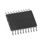
ICGOO电子元器件商城为您提供AD7927BRUZ由Analog设计生产,在icgoo商城现货销售,并且可以通过原厂、代理商等渠道进行代购。 AD7927BRUZ价格参考。AnalogAD7927BRUZ封装/规格:数据采集 - 模数转换器, 12 Bit Analog to Digital Converter 8 Input 1 SAR 20-TSSOP。您可以下载AD7927BRUZ参考资料、Datasheet数据手册功能说明书,资料中有AD7927BRUZ 详细功能的应用电路图电压和使用方法及教程。
AD7927BRUZ 是由 Analog Devices Inc.(ADI)生产的一款高性能 16 位模数转换器(ADC),属于数据采集系统中的核心元件。其应用场景广泛,尤其是在需要高精度、高速度和低功耗的数据采集领域。以下是该型号的主要应用场景:

1. 工业自动化与控制
   AD7927BRUZ 可用于工业自动化设备中,例如可编程逻辑控制器(PLC)、数据采集模块和传感器接口。它能够精确地将模拟信号(如温度、压力、流量等传感器输出)转换为数字信号,以便进行后续处理和分析。

2. 医疗设备
   在医疗设备中,如心电图(ECG)、血压监测仪和超声波设备,AD7927BRUZ 提供了高分辨率和低噪声的性能,确保对生物信号的准确采集和分析,从而提高诊断精度。

3. 通信系统
   该 ADC 适用于通信领域的信号处理,例如软件定义无线电(SDR)和基站接收机。其快速采样能力和低失真特性使其能够高效处理复杂的射频信号。

4. 测试与测量仪器
   在示波器、频谱分析仪和其他精密测试设备中,AD7927BRUZ 的高线性度和动态范围使其成为理想选择,可以满足对信号质量要求极高的测试需求。

5. 汽车电子
   该器件可用于汽车电子系统中,例如发动机控制单元(ECU)和车载传感器网络。其抗干扰能力和稳定性有助于在恶劣环境下实现可靠的信号采集。

6. 能源管理
   在智能电网和能源管理系统中,AD7927BRUZ 能够精确监测电压、电流和其他关键参数,帮助优化能源使用并提高效率。

总之,AD7927BRUZ 凭借其卓越的性能指标,适用于需要高精度和高可靠性的各种应用场景,特别是在工业、医疗、通信和汽车等领域发挥重要作用。
| 参数 | 数值 |
| 产品目录 | 集成电路 (IC)半导体 |
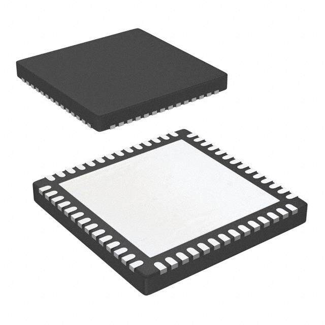
| 描述 | IC ADC 12BIT 8CH 200KSPS 20TSSOP模数转换器 - ADC 8CH 200 kSPS 12-Bit W/ Sequencer |
| 产品分类 | |
| 品牌 | Analog Devices |
| 产品手册 | |
| 产品图片 |
|
| rohs | 符合RoHS无铅 / 符合限制有害物质指令(RoHS)规范要求 |
| 产品系列 | 数据转换器IC,模数转换器 - ADC,Analog Devices AD7927BRUZ- |
| 数据手册 | |
| 产品型号 | AD7927BRUZ |
| 产品目录页面 | |
| 产品种类 | 模数转换器 - ADC |
| 位数 | 12 |
| 供应商器件封装 | 20-TSSOP |
| 信噪比 | 70 dB |
| 分辨率 | 12 bit |
| 包装 | 管件 |
| 商标 | Analog Devices |
| 安装类型 | 表面贴装 |
| 安装风格 | SMD/SMT |
| 封装 | Tube |
| 封装/外壳 | 20-TSSOP(0.173",4.40mm 宽) |
| 封装/箱体 | TSSOP-20 |
| 工作温度 | -40°C ~ 85°C |
| 工作电源电压 | 5 V |
| 工厂包装数量 | 75 |
| 接口类型 | Serial (SPI, QSPI, Microwire) |
| 数据接口 | DSP,MICROWIRE™,QSPI™,串行,SPI™ |
| 最大功率耗散 | 7.5 mW |
| 最大工作温度 | + 85 C |
| 最小工作温度 | - 40 C |
| 标准包装 | 75 |
| 特性 | - |
| 电压参考 | External |
| 电压源 | 单电源 |
| 系列 | AD7927 |
| 结构 | SAR |
| 转换器数 | 1 |
| 转换器数量 | 1 |
| 转换速率 | 200 kS/s |
| 输入数和类型 | 8 个单端,单极 |
| 输入类型 | Single-Ended |
| 通道数量 | 8 Channel |
| 配用 | /product-detail/zh/EVAL-AD7927CBZ/EVAL-AD7927CBZ-ND/1644964 |
| 采样率(每秒) | 200k |


- 商务部:美国ITC正式对集成电路等产品启动337调查
- 曝三星4nm工艺存在良率问题 高通将骁龙8 Gen1或转产台积电
- 太阳诱电将投资9.5亿元在常州建新厂生产MLCC 预计2023年完工
- 英特尔发布欧洲新工厂建设计划 深化IDM 2.0 战略
- 台积电先进制程称霸业界 有大客户加持明年业绩稳了
- 达到5530亿美元!SIA预计今年全球半导体销售额将创下新高
- 英特尔拟将自动驾驶子公司Mobileye上市 估值或超500亿美元
- 三星加码芯片和SET,合并消费电子和移动部门,撤换高东真等 CEO
- 三星电子宣布重大人事变动 还合并消费电子和移动部门
- 海关总署:前11个月进口集成电路产品价值2.52万亿元 增长14.8%


PDF Datasheet 数据手册内容提取
8-Channel, 200 kSPS, 12-Bit ADC with Sequencer in 20-Lead TSSOP Data Sheet AD7927 FEATURES FUNCTIONAL BLOCK DIAGRAM Fast throughput rate: 200 kSPS AVDD Specified for AV of 2.7 V to 5.25 V DD Low power REFIN 3.6 mW maximum at 200 kSPS with 3 V supply VIN0 12-BIT SUCCESSIVE 7.5 mW maximum at 200 kSPS with 5 V supply T/H APPROXIMATION 8 (single-ended) inputs with sequencer INPUT ADC MUX Wide input bandwidth 70 dB minimum SINAD at 50 kHz input frequency Flexible power/serial clock speed management No pipeline delays VIN7 SCLK High speed serial interface SPI-, QSPI™-, MICROWIRE™-, DOUT DSP-compatible SEQUENCER CONTROL LOGIC DIN Shutdown mode: 0.5 μA maximum CS 20-lead TSSOP AD7927 QGuEaNliEfiRedA fLo rD aEuStoCmRoItPivTeI OapNp lications AGND VDRIVE 03088-001 Figure 1. The AD7927 is a 12-bit, high speed, low power, 8-channel, PRODUCT HIGHLIGHTS successive approximation ADC. The part operates from a single 2.7 V to 5.25 V power supply and features throughput 1. High Throughput with Low Power Consumption. rates up to 200 kSPS. The part contains a low noise, wide The AD7927 offers up to 200 kSPS throughput rates. At the bandwidth track-and-hold amplifier that can handle input maximum throughput rate with 3 V supplies, the AD7927 frequencies in excess of 8 MHz. dissipates 3.6 mW of power maximum. The conversion process and data acquisition are controlled using 2. Eight Single-Ended Inputs with a Channel Sequencer. CS and the serial clock signal, allowing the device to easily interface A consecutive sequence of channels can be selected on with microprocessors or DSPs. The input signal is sampled on the which the ADC cycles and converts. falling edge of CS and the conversion is also initiated at this 3. Single-Supply Operation with VDRIVE Function. point. There are no pipeline delays associated with the part. The AD7927 operates from a single 2.7 V to 5.25 V supply. The V function allows the serial interface to connect The AD7927 uses advanced design techniques to achieve DRIVE directly to either 3 V or 5 V processor systems independent very low power dissipation at maximum throughput rates. At of AV . maximum throughput rates, the AD7927 consumes 1.2 mA DD maximum with 3 V supplies; with 5 V supplies, the current 4. Flexible Power/Serial Clock Speed Management. consumption is 1.5 mA maximum. The conversion rate is determined by the serial clock, Through the configuration of the control register, the analog allowing the conversion time to be reduced through the input range for the part can be selected as 0 V to REF or 0 V serial clock speed increase. The part also features various IN shutdown modes to maximize power efficiency at lower to 2 × REF , with either straight binary or twos complement IN throughput rates. Current consumption is 0.5 μA maxi- output coding. The AD7927 features eight single-ended analog mum when in full shutdown. inputs with a channel sequencer to allow a preprogrammed selection of channels to be converted sequentially. 5. No Pipeline Delay. The part features a standard successive approximation ADC The conversion time for the AD7927 is determined by the SCLK frequency, as this is also used as the master clock to with a CS input pin, which allows for accurate control of control the conversion. The conversion time may be as short each sampling instant. as 800 ns with a 20 MHz SCLK. Rev. D Document Feedback Information furnished by Analog Devices is believed to be accurate and reliable. However, no responsibility is assumed by Analog Devices for its use, nor for any infringements of patents or other One Technology Way, P.O. Box 9106, Norwood, MA 02062-9106, U.S.A. rights of third parties that may result from its use. Specifications subject to change without notice. No license is granted by implication or otherwise under any patent or patent rights of Analog Devices. Tel: 781.329.4700 ©2003–2013 Analog Devices, Inc. All rights reserved. Trademarks and registered trademarks are the property of their respective owners. Technical Support www.analog.com
AD7927 Data Sheet TABLE OF CONTENTS Features .............................................................................................. 1 Analog Input Selection .............................................................. 17 General Description ......................................................................... 1 Digital Inputs .............................................................................. 17 Functional Block Diagram .............................................................. 1 V ............................................................................................ 18 DRIVE Product Highlights ........................................................................... 1 The Reference ............................................................................. 18 Revision History ............................................................................... 2 Modes of Operation ....................................................................... 19 Specifications ..................................................................................... 3 Normal Mode (PM1 = PM0 = 1) ............................................. 19 Timing Specifications .................................................................. 5 Full Shutdown (PM1 = 1, PM0 = 0) ........................................ 19 Absolute Maximum Ratings ............................................................ 6 Auto Shutdown (PM1 = 0, PM0 = 1) ....................................... 20 ESD Caution .................................................................................. 6 Powering Up the AD7927 ......................................................... 21 Pin Configuration and Function Descriptions ............................. 7 Power vs. Throughput Rate ....................................................... 21 Terminology ...................................................................................... 8 Serial Interface ................................................................................ 22 Typical Performance Characteristics ........................................... 10 Writing Between Conversions .................................................. 22 Control Register .............................................................................. 12 Microprocessor Interfacing ........................................................... 24 Sequencer Operation ...................................................................... 13 AD7927 to TMS320C541 .......................................................... 24 Shadow Register .............................................................................. 14 AD7927 to ADSP-21xx .............................................................. 24 Circuit Information .................................................................... 15 AD7927 to DSP563xx ................................................................ 25 Converter Operation .................................................................. 15 Application Hints ........................................................................... 26 Analog Input ............................................................................... 15 Grounding and Layout .............................................................. 26 ADC Transfer Function ............................................................. 16 Outline Dimensions ....................................................................... 27 Handling Bipolar Input Signals ................................................ 16 Ordering Guide .......................................................................... 27 Typical Connection Diagram ........................................................ 17 Automotive Products ................................................................. 27 REVISION HISTORY 12/08—Rev. A to Rev. B 6/13—Rev. C to Rev. D Changes to ESD Parameter, Table 3 ................................................ 6 Deleted Evaluating the AD7927 Performance Section .............. 26 Changes to Ordering Guide .......................................................... 27 Changes to Ordering Guide .......................................................... 27 1/07—Rev. 0 to Rev. A 12/11—Rev. B to Rev. C Updated Format .................................................................. Universal Changes to Features Section............................................................ 1 Updated Layout ................................................................................. 8 Changes to Table 1 ............................................................................ 3 Updated Layout .............................................................................. 10 Changes to Table 3 ............................................................................ 6 Changes to Figure 12 Caption ...................................................... 14 Changes to Ordering Guide, Added Automotive Products Changes to Figure 13 Caption ...................................................... 15 Section .............................................................................................. 27 Changes to Ordering Guide .......................................................... 27 1/03—Revision 0: Initial Version Rev. D | Page 2 of 28
Data Sheet AD7927 SPECIFICATIONS AV = V = 2.7 V to 5.25 V, REF = 2.5 V, f = 20 MHz; T = T to T , unless otherwise noted. DD DRIVE IN SCLK A MIN MAX Table 1. Parameter B Version1 Unit Test Conditions/Comments DYNAMIC PERFORMANCE f = 50 kHz sine wave, f = 20 MHz IN SCLK Signal-to-(Noise + Distortion) (SINAD)2 70 dB min @ 5 V, B models 69.5 dB min @ 5 V, W models 69 dB min @ 3 V Typically 70 dB Signal-to-Noise Ratio (SNR)2 70 dB min B models 69.5 dB min W models Total Harmonic Distortion (THD) 2 −77 dB max @ 5 V Typically −84 dB −73 dB max @ 3 V Typically −77 dB Peak Harmonic or Spurious Noise −78 dB max @ 5 V Typically −86 dB (SFDR) 2 −76 dB max @ 3 V Typically −80 dB Intermodulation Distortion (IMD)2 f = 40.1 kHz, f = 41.5 kHz A B Second-Order Terms −90 dB typ Third-Order Terms −90 dB typ Aperture Delay 10 ns typ Aperture Jitter 50 ps typ Channel-to-Channel Isolation2 −82 dB typ f = 400 kHz IN Full Power Bandwidth 8.2 MHz typ @ 3 dB 1.6 MHz typ @ 0.1 dB DC ACCURACY2 Resolution 12 Bits Integral Nonlinearity ±1 LSB max Differential Nonlinearity −0.9/+1.5 LSB max Guaranteed no missed codes to 12 bits 0 V to REF Input Range Straight binary output coding IN Offset Error ±8 LSB max Typically ±0.5 LSB Offset Error Match ±0.5 LSB max Gain Error ±1.5 LSB max Gain Error Match ±0.5 LSB max 0 V to 2 × REF Input Range −REF to +REF biased about REF with IN IN IN IN Positive Gain Error ±1.5 LSB max Twos complement output coding Positive Gain Error Match ±0.5 LSB max Zero Code Error ±8 LSB max Typically ±0.8 LSB Zero Code Error Match ±0.5 LSB max Negative Gain Error ±1 LSB max Negative Gain Error Match ±0.5 LSB max ANALOG INPUT Input Voltage Ranges 0 to REF V RANGE bit set to 1 IN 0 to 2 × REF V RANGE bit set to 0, AV /V = 4.75 V to 5.25 V IN DD DRIVE DC Leakage Current ±1 μA max Input Capacitance 20 pF typ f = 200 kSPS SAMPLE REFERENCE INPUT REF Input Voltage 2.5 V ±1% specified performance IN DC Leakage Current ±1 μA max REF Input Impedance 36 kΩ typ IN LOGIC INPUTS Input High Voltage, V 0.7 × V V min INH DRIVE Input Low Voltage, V 0.3 × V V max INL DRIVE Input Current, I ±1 μA max Typically 10 nA, V = 0 V or V IN IN DRIVE Input Capacitance, C 3 10 pF max IN Rev. D | Page 3 of 28
AD7927 Data Sheet Parameter B Version1 Unit Test Conditions/Comments LOGIC OUTPUTS Output High Voltage, V V − 0.2 V min I = 200 μA, AV = 2.7 V to 5.25 V OH DRIVE SOURCE DD Output Low Voltage, V 0.4 V max I = 200 μA OL SINK Floating-State Leakage Current ±1 μA max Floating-State Output Capacitance3 10 pF max Output Coding Straight (Natural) Binary Coding bit set to 1 Twos Complement Coding bit set to 0 CONVERSION RATE Conversion Time 800 ns max 16 SCLK cycles with SCLK at 20 MHz Track-and-Hold Acquisition Time 300 ns max Sine wave input 300 ns max Full-scale step input Throughput Rate 200 kSPS max See Serial Interface section POWER REQUIREMENTS AV 2.7/5.25 V min/max DD V 2.7/5.25 V min/max DRIVE I 4 Digital inputs = 0 V or V DD DRIVE During Conversion 2.7 mA max AV = 4.75 V to 5.25 V, f = 20 MHz DD SCLK 2 mA max AV = 2.7 V to 3.6 V, f = 20 MHz DD SCLK Normal Mode (Static) 600 μA typ AV = 2.7 V to 5.25 V, SCLK on or off DD Normal Mode (Operational) f = 200 kSPS 1.5 mA max AV = 4.75 V to 5.25 V, f = 20 MHz SAMPLE DD SCLK 1.2 mA max AV = 2.7 V to 3.6 V, f = 20 MHz DD SCLK Using Auto Shutdown Mode f = 200 kSPS 900 μA typ AV = 4.75 V to 5.25 V, f = 20 MHz SAMPLE DD SCLK 650 μA typ AV = 2.7 V to 3.6 V, f = 20 MHz DD SCLK Auto Shutdown (Static) 0.5 μA max SCLK on or off (20 nA typ) Full Shutdown Mode 0.5 μA max SCLK on or off (20 nA typ) Power Dissipation4 Normal Mode (Operational) 7.5 mW max AV = 5 V, f = 20 MHz DD SCLK 3.6 mW max AV = 3 V, f = 20 MHz DD SCLK Auto Shutdown (Static) 2.5 μW max AV = 5 V DD 1.5 μW max AV = 3 V DD Full Shutdown Mode 2.5 μW max AV = 5 V DD 1.5 μW max AV = 3 V DD 1 Temperature ranges as follows: B Version: −40°C to +85°C; W Version: −40°C to +125°C. 2 See Terminology section. 3 Sample tested @ 25°C to ensure compliance. 4 See Power vs. Throughput Rate section. Rev. D | Page 4 of 28
Data Sheet AD7927 TIMING SPECIFICATIONS1 AV = 2.7 V to 5.25 V, V ≤ AV , REF = 2.5 V; T = T to T , unless otherwise noted. DD DRIVE DD IN A MIN MAX Table 2. Limit at T , T AD7927 MIN MAX Parameter AV = 3 V AV = 5 V Unit Description DD DD f 2 10 10 kHz min SCLK 20 20 MHz max t 16 × t 16 × t CONVERT SCLK SCLK t 50 50 ns min Minimum quiet time required between CS rising edge and start of QUIET next conversion t 10 10 ns min CS to SCLK setup time 2 t3 35 30 ns max Delay from CS until DOUT three-state disabled 3 t3 40 40 ns max Data access time after SCLK falling edge 4 t 0.4 × t 0.4 × t ns min SCLK low pulsewidth 5 SCLK SCLK t 0.4 × t 0.4 × t ns min SCLK high pulsewidth 6 SCLK SCLK t 10 10 ns min SCLK to DOUT valid hold time 7 t4 15/45 15/35 ns min/max SCLK falling edge to DOUT high impedance 8 t 10 10 ns min DIN setup time prior to SCLK falling edge 9 t 5 5 ns min DIN hold time after SCLK falling edge 10 t 20 20 ns min Sixteenth SCLK falling edge to CS high 11 t 1 1 μs max Power-up time from full power-down/auto shutdown mode 12 1 Sample tested at 25°C to ensure compliance. All input signals are specified with tr = tf = 5 ns (10% to 90% of AVDD) and timed from a voltage level of 1.6 V, (see Figure 2). The 3 V operating range spans from 2.7 V to 3.6 V. The 5 V operating range spans from 4.75 V to 5.25 V. 2 Mark/space ratio for the SCLK input is 40/60 to 60/40. 3 Measured with the load circuit of Figure 2 and defined as the time required for the output to cross 0.4 V or 0.7 × VDRIVE. 4 t8 is derived from the measured time taken by the data outputs to change 0.5 V when loaded with the circuit of Figure 2. The measured number is then extrapolated back to remove the effects of charging or discharging the 50 pF capacitor. This means the time, quoted in the t8 timing characteristics, is the true bus relinquish time of the part and is independent of the bus loading. 200µA IOL TO OUTPUT 1.6V PIN CL 50pF 200µA IOH 03088-002 Figure 2. Load Circuit for Digital Output Timing Specifications Rev. D | Page 5 of 28
AD7927 Data Sheet ABSOLUTE MAXIMUM RATINGS T = 25°C, unless otherwise noted. A Table 3. Stresses above those listed under Absolute Maximum Ratings Parameter Rating may cause permanent damage to the device. This is a stress rating only; functional operation of the device at these or any AV to AGND −0.3 V to +7 V DD other conditions above those indicated in the operational V to AGND −0.3 V to AV + 0.3 V DRIVE DD section of this specification is not implied. Exposure to absolute Analog Input Voltage to AGND −0.3 V to AV + 0.3 V DD maximum rating conditions for extended periods may affect Digital Input Voltage to AGND −0.3 V to +7 V device reliability. Digital Output Voltage to AGND −0.3 V to AV + 0.3 V DD REFIN to AGND −0.3 V to AVDD + 0.3 V ESD CAUTION Input Current to Any Pin Except Supplies1 ±10 mA Operating Temperature Range Commercial (B Version) −40°C to +85°C Automotive (W Version) −40°C to +125°C Storage Temperature Range −65°C to +150°C Junction Temperature 150°C TSSOP, Power Dissipation 450 mW θ Thermal Impedance 143°C/W (TSSOP) JA θ Thermal Impedance 45°C/W (TSSOP) JC Lead Temperature, Soldering Vapor Phase (60 sec) 215°C Infrared (15 sec) 220°C ESD 1.5 kV 1 Transient currents of up to 100 mA do not cause SCR latch-up. Rev. D | Page 6 of 28
Data Sheet AD7927 PIN CONFIGURATION AND FUNCTION DESCRIPTIONS SCLK 1 20 AGND DIN 2 19 VDRIVE CS 3 18 DOUT AD7927 AGND 4 TOP VIEW 17 AGND AVDD 5 (Not to Scale) 16 VIN0 AVDD 6 15 VIN1 REFIN 7 14 VIN2 AGND 8 13 VIN3 VIN7 9 12 VIN4 VIN6 10 11 VIN5 03088-003 Figure 3. 20-Lead TSSOP Pin Configuration Table 4. Pin Function Descriptions Pin No. Mnemonic Description 1 SCLK Serial Clock. Logic input. SCLK provides the serial clock for accessing data from the part. This clock input is also used as the clock source for the AD7927 conversion process. 2 DIN Data In. Logic input. Data to be written to the AD7927 control register is provided on this input and is clocked into the register on the falling edge of SCLK (see the Control Register section). 3 CS Chip Select. Active low logic input. This input provides the dual function of initiating conversions on the AD7927 and framing the serial data transfer. 4, 8, 17, 20 AGND Analog Ground. Ground reference point for all analog circuitry on the AD7927. All analog input signals and any external reference signal should be referred to this AGND voltage. All AGND pins should be connected together. 5, 6 AV Analog Power Supply Input. The AV range for the AD7927 is from 2.7 V to 5.25 V. For the 0 V to 2 × REF DD DD IN range, AV should be from 4.75 V to 5.25 V. DD 7 REF Reference Input for the AD7927. An external reference must be applied to this input. The voltage range for IN the external reference is 2.5 V ±1% for specified performance. 16 to 9 V 0 to V 7 Analog Input 0 through Analog Input 7. Eight single-ended analog input channels that are multiplexed into IN IN the on-chip track-and-hold. The analog input channel to be converted is selected by using the address bits (ADD2 through ADD0) of the control register. ADD2 through ADD0, in conjunction with the SEQ and SHADOW bits, allow the sequencer to be programmed. The input range for all input channels can extend from 0 V to REF or 0 V to 2 × REF , as selected via the RANGE bit in the control register. Any unused input IN IN channels should be connected to AGND to avoid noise pickup. 18 DOUT Data Out. Logic output. The conversion result from the AD7927 is provided on this output as a serial data stream. The bits are clocked out on the falling edge of the SCLK input. The data stream from the AD7927 consists of two leading zeros, two address bits indicating which channel the conversion result corresponds to, followed by the 12 bits of conversion data (MSB first). The output coding may be selected as straight binary or twos complement via the CODING bit in the control register. 19 V Logic Power Supply Input. The voltage supplied at this pin determines at what voltage the serial interface of DRIVE the AD7927 operates. Rev. D | Page 7 of 28
AD7927 Data Sheet TERMINOLOGY Integral Nonlinearity (INL) Negative Gain Error INL is the maximum deviation from a straight line passing This applies when using the twos complement output coding through the endpoints of the ADC transfer function. The end- option, in particular to the 2 × REF input range with −REF IN IN points of the transfer function are zero scale, a point 1 LSB to +REF biased about the REF point. It is the deviation of IN IN below the first code transition, and full scale, a point 1 LSB the first code transition (100 . . . 000) to (100 . . . 001) from the above the last code transition. Figure 9 shows a typical INL ideal (that is, −REF + 1 LSB) after the zero code error has been IN plot for the AD7927. adjusted out. Differential Nonlinearity (DNL) Negative Gain Error Match DNL is the difference between the measured and the ideal This is the difference in negative gain error between any two 1 LSB change between any two adjacent codes in the ADC. channels. Figure 10 shows a typical DNL plot for the AD7927. Channel-to-Channel Isolation Offset Error Channel-to-channel isolation is a measure of the level of This is the deviation of the first code transition (00 . . . 000) to crosstalk between channels. It is measured by applying a full- (00 . . . 001) from the ideal, that is, AGND + 1 LSB. scale 400 kHz sine wave signal to all seven nonselected input channels and determining how much that signal is attenuated Offset Error Match in the selected channel with a 50 kHz signal. The figure given is This is the difference in offset error between any two channels. the worst case across all eight channels for the AD7927. Gain Error Power Supply Rejection (PSR) This is the deviation of the last code transition (111 . . . 110) to Variations in power supply affect the full-scale transition, (111 . . . 111) from the ideal (that is, REF − 1 LSB) after the IN but not the converter’s linearity. Power supply rejection is the offset error has been adjusted out. maximum change in full-scale transition point due to a change in power supply voltage from the nominal value (see the Typical Gain Error Match Performance Characteristics section). This is the difference in gain error between any two channels. Power Supply Rejection Ration (PSRR) Zero Code Error The power supply rejection ratio is defined as the ratio of the This applies when using the twos complement output coding power in the ADC output at full-scale frequency (f) to the option, in particular to the 2 × REF input range with −REF IN IN power of a 200 mV p-p sine wave applied to the ADC AV to +REF biased about the REF point. It is the deviation of DD IN IN supply of frequency (f): the midscale transition (all 0s to all 1s) from the ideal V S IN voltage, that is, REF − 1 LSB. PSRR(dB) = 10log(Pf/Pf) IN S where: Zero Code Error Match Pf is equal to the power at Frequency f in ADC output. This is the difference in zero code error between any two Pf is equal to the power at Frequency f coupled onto the channels. S S ADC AV . DD Positive Gain Error Here a 200 mV p-p sine wave is coupled onto the AV supply. DD This applies when using the twos complement output coding Figure 6 shows the power supply rejection ratio vs. supply ripple option, in particular to the 2 × REF input range with −REF IN IN frequency for the AD7927 with no decoupling. to +REF biased about the REF point. It is the deviation of the IN IN last code transition (011. . .110) to (011 . . . 111) from the ideal Track-and-Hold Acquisition Time (that is, +REF − 1 LSB) after the zero code error has been The track-and-hold amplifier returns into track mode at the IN adjusted out. end of conversion. Track-and-hold acquisition time is the time required for the output of the track-and-hold amplifier to reach Positive Gain Error Match its final value, within ±1 LSB, after the end of conversion. This is the difference in positive gain error between any two channels. Rev. D | Page 8 of 28
Data Sheet AD7927 Total Harmonic Distortion (THD) Signal-to-(Noise + Distortion) Ratio (SINAD) THD is the ratio of the rms sum of harmonics to the This is the measured ratio of signal-to-(noise + distortion) at fundamental. For the AD7927, it is defined as: the output of the ADC. The signal is the rms amplitude of the fundamental. Noise is the sum of all nonfundamental signals V2V2V2V2V2 up to half the sampling frequency (f/2), excluding dc. The ratio THD(dB)20log 2 3 4 5 6 S V is dependent on the number of quantization levels in the digiti- 1 zation process; the more levels, the smaller the quantization where: noise. The theoretical signal-to-(noise + distortion) ratio for V1 is the rms amplitude of the fundamental. an ideal N-bit converter with a sine wave input is given by V, V, V, V, and V are the rms amplitudes of the second 2 3 4 5 6 through the sixth harmonics. Signal-to-(Noise + Distortion) = (6.02N + 1.76)dB Figure 7 shows a graph of total harmonic distortion vs. analog Thus, for a 12-bit converter, this is 74 dB. Figure 5 shows the input frequency for various supply voltages, and Figure 8 shows signal-to-(noise + distortion) ratio performance vs. input fre- a graph of total harmonic distortion vs. analog input frequency quency for various supply voltages while sampling at 200 kSPS for various source impedances (see the Analog Input section). with an SCLK of 20 MHz. Rev. D | Page 9 of 28
AD7927 Data Sheet TYPICAL PERFORMANCE CHARACTERISTICS 0 4096 POINT FFT AVDD = 5V AVDD = 4.75V –10 200mV p-p SINEWAVE ONAVDD –10 fSAMPLE = 200kSPS REFIN = 2.5V, 1µF CAPACITOR fIN= 50kHz –20 TA = 25°C SINAD = 70.714dB THD = –82.853dB –30 –30 SFDR = –84.815dB B) dB)–40 NR (d–50 SRR (–50 S P –70 –60 –70 –90 –80 –1100 10 20 30 FR4E0QUE5N0CY (k6H0z) 70 80 90 100 03088-004 –900 20 40SUP6P0LY RI8P0PLE1 F00REQ1U2E0NC1Y4 (0kHz1)60 180 200 03088-006 Figure 4. Dynamic Performance at 200 kSPS Figure 6. PSRR vs. Supply Ripple Frequency 75 –50 fSAMPLE = 200kSPS –55 TA = 25°C AVDD =VDRIVE = 5.25V RANGE = 0TO REFIN AVDD =VDRIVE = 4.75V –60 70 B) –65 SINAD (d AAVVDDDD ==VVDDRRIIVVEE == 32..67VV THD (dB)–70 AVDD =VDRIVE = 2.7V –75 65 AVDD =VDRIVE = 3.6V –80 fSAMPLE = 200kSPS TA = 25°C –85 RANGE = 0 TO REFIN AVDD =VDRIVE = 4.75V 600 INPUT FREQUENCY (kHz) 100 03088-005 –9010 INPUT FREQUENCY (kAHVzD)D =VDRIVE = 5.25V100 03088-007 Figure 5. SINAD vs. Analog Input Frequency for Various Supply Voltages Figure 7. THD vs. Analog Input Frequency for Various Supply Voltages at 200 kSPS at 200 kSPS Rev. D | Page 10 of 28
Data Sheet AD7927 –55 fSAMPLE = 200kSPS 1.0 –60 TA = 25°C AVDD =VDRIVE= 5V AVDD = 5.25V 0.8 TA = 25°C RANGE = 0TO REFIN –65 0.6 0.4 THD (dB) ––7705 RIN = 1000Ω RROR (LSB) 0.20 –80 RIN = 100Ω RIN = 10Ω NL E–0.2 D –85 –0.4 –0.6 –90 RIN = 50Ω –0.8 Figure–9 85.1 T0HD vs. Analog InIpNuPtU FTr FeRquEQenUcEyN fCoYr V(kaHrzi)ous Source Impe1d00an03088-008ces –1.00 512 1024 1536 C20O4D8E 2560 3072 3584 4096 03088-010 Figure 10. Typical DNL 1.0 0.8 AVDD =VDRIVE= 5V TA = 25°C 0.6 0.4 B) LS 0.2 R ( O 0 R R L E–0.2 N I –0.4 –0.6 –0.8 –1.00 512 1024 1536 C20O4D8E 2560 3072 3584 4096 03088-009 Figure 9. Typical INL Rev. D | Page 11 of 28
AD7927 Data Sheet CONTROL REGISTER The control register on the AD7927 is a 12-bit, write-only register. Data is loaded from the DIN pin of the AD7927 on the falling edge of SCLK. The data is transferred on the DIN line at the same time that the conversion result is read from the part. The data transferred on the DIN line corresponds to the AD7927 configuration for the next conversion. This requires 16 serial clocks for every data transfer. Only the information provided on the first 12 falling clock edges (after CS falling edge) is loaded to the control register. MSB denotes the first bit in the data stream. The bit functions are outlined in Table 5. Table 5. Control Register Bit Functions MSB LSB WRITE SEQ DONTC ADD2 ADD1 ADD0 PM1 PM0 SHADOW DONTC RANGE CODING Table 6. Control Register Bit Function Description Bit Mnemonic Description 11 WRITE The value written to this bit of the control register determines whether the following 11 bits are loaded to the control register. If this bit is a 1, the following 11 bits are written to the control register; if it is a 0, then the remaining 11 bits are not loaded to the control register and it remains unchanged. 10 SEQ The SEQ bit in the control register is used in conjunction with the SHADOW bit to control the use of the sequencer function and access the shadow register (see Table 10). 9 DONTC Don’t care. 8 to 6 ADD2 to These three address bits are loaded at the end of the present conversion and select which analog input channel ADD0 is to be converted in the next serial transfer, or they may select the final channel in a consecutive sequence as described in Table 9. The selected input channel is decoded as shown in Table 7. The address bits corresponding to the conversion result are also output on DOUT prior to the 12 bits of data (see the Serial Interface section). The next channel to be converted on is selected by the mux on the 14th SCLK falling edge. 5, 4 PM1, PM0 Power Management Bits. These two bits decode the mode of operation of the AD7927 as shown in Table 8. 3 SHADOW The SHADOW bit in the control register is used in conjunction with the SEQ bit to control the use of the sequencer function and access the shadow register (see Table 10). 2 DONTC Don’t care. 1 RANGE This bit selects the analog input range to be used on the AD7927. If it is set to 0, the analog input range extends from 0 V to 2 × REF . If it is set to 1, the analog input range extends from 0 V to REF (for the next conversion). For IN IN the 0 V to 2 × REF range, AV = 4.75 V to 5.25 V. IN DD 0 CODING This bit selects the type of output coding the AD7927 uses for the conversion result. If this bit is set to 0, the output coding for the part is twos complement. If this bit is set to 1, the output coding from the part is straight binary (for the next conversion). Table 7. Channel Selection ADD2 ADD1 ADD0 Analog Input Channel 0 0 0 V 0 IN 0 0 1 V 1 IN 0 1 0 V 2 IN 0 1 1 V 3 IN 1 0 0 V 4 IN 1 0 1 V 5 IN 1 1 0 V 6 IN 1 1 1 V 7 IN Table 8. Power Mode Selection PM1 PM0 Mode 1 1 Normal Operation. In this mode, the AD7927 remains in full power mode, regardless of the status of any of the logic inputs. This mode allows the fastest possible throughput rate from the AD7927. 1 0 Full Shutdown. In this mode, the AD7927 is in full shutdown mode with all circuitry on the AD7927 powering down. The AD7927 retains the information in the control register while in full shutdown. The part remains in full shutdown until these bits are changed. 0 1 Auto Shutdown. In this mode, the AD7927 automatically enters full shutdown mode at the end of each conversion when the control register is updated. Wake-up time from full shutdown is 1 μs and the user should ensure that 1 μs has elapsed before attempting to perform a valid conversion on the part in this mode. 0 0 Invalid Selection. This configuration is not allowed. Rev. D | Page 12 of 28
Data Sheet AD7927 SEQUENCER OPERATION The configuration of the SEQ and SHADOW bits in the control register allows the user to select a particular mode of operation of the sequencer function. Table 9 outlines the four modes of operation of the sequencer. Table 9. Sequence Selection SEQ SHADOW Sequence Type 0 0 This configuration means that the sequence function is not used. The analog input channel selected for each individual conversion is determined by the contents of the channel address bits, ADD0 through ADD2, in each prior write operation. This mode of operation reflects the traditional operation of a multichannel ADC, without the sequencer function being used, where each write to the AD7927 selects the next channel for conversion (see Figure 11). 0 1 This configuration selects the shadow register for programming. The following write operation loads the contents of the shadow register. This programs the sequence of channels converted on continuously with each successive valid CS falling edge (see the Shadow Register section, Table 10, and Figure 12). The channels selected need not be consecutive. 1 0 If the SEQ and SHADOW bits are set in this way, the sequence function is not interrupted upon completion of the WRITE operation. This allows other bits in the control register to be altered between conversions while in a sequence, without terminating the cycle. 1 1 This configuration is used in conjunction with the channel address bits, ADD2 to ADD0, to program continuous conversions on a consecutive sequence of channels from Channel 0 to a selected final channel as determined by the channel address bits in the control register (see Figure 13). Rev. D | Page 13 of 28
AD7927 Data Sheet SHADOW REGISTER Table 10. Shadow Register Bit Functions MSB LSB V 0 V 1 V 2 V 3 V 4 V 5 V 6 V 7 V 0 V 1 V 2 V 3 V 4 V 5 V 6 V 7 IN IN IN IN IN IN IN IN IN IN IN IN IN IN IN IN --------------------------------SEQUENCE ONE-------------------------------- --------------------------------SEQUENCE TWO-------------------------------- The shadow register on the AD7927 is a 16-bit, write-only register. Figure 12 shows how to program the AD7927 to continuously Data is loaded from the DIN pin of the AD7927 on the falling convert on a particular sequence of channels. To exit this mode edge of SCLK. The data is transferred on the DIN line at the of operation and revert back to the traditional mode of opera- same time that a conversion result is read from the part. This tion of a multichannel ADC (as outlined in Figure 11), ensure requires 16 serial clock falling edges for the data transfer. The that the WRITE bit = 1 and the SEQ = SHADOW = 0 on the information is clocked into the shadow register, provided that next serial transfer. Figure 13 shows how a sequence of consecu- the SEQ and SHADOW bits were set to 0, 1, respectively, in the tive channels can be converted on without having to program previous write to the control register. MSB denotes the first bit the shadow register or write to the part on each serial transfer. in the data stream. Each bit represents an analog input from Again, to exit this mode of operation and revert back to the Channel 0 to Channel 7. Through programming the shadow traditional mode of operation of a multichannel ADC (as register, two sequences of channels may be selected, through outlined in Figure 11), ensure the WRITE bit = 1 and the which the AD7927 cycles with each consecutive conversion SEQ = SHADOW = 0 on the next serial transfer. after the write to the shadow register. Sequence One is per- formed first and then Sequence Two. If the user does not POWER-ON wish to perform a second sequence option, then all 0s must be DUMMY CONVERSION written to the last eight LSBs of the shadow register. To select a DIN = ALL 1s sequence of channels, the associated channel bit must be set for each analog input. The AD7927 continuously cycles through DIN: WRITE TO CONTROL REGISTER, WRITE BIT = 1, CS the selected channels in ascending order, beginning with the SELECT CODING, RANGE, AND POWER MODE. SELECT CHANNEL A2 TO CHANNEL A0 lowest channel, until a write operation occurs (that is, the WRITE FOR CONVERSION. SEQ = 0, SHADOW = 1 bit is set to 1) with the SEQ and SHADOW bits configured in any way except 1, 0 (see Table 9). The bit functions are outlined in Table 10. DOUT: CONVERSION RESULT FROM PREVIOUSLY POWER-ON CS SELECTED CHANNEL A2 TO CHANNEL A0. DIN: WRITE TO SHADOW REGISTER, SELECTING WHICH CHANNELS TO CONVERT ON; CHANNELS DUMMY CONVERSION SELECTEDNEEDNOTBECONSECUTIVECHANNELS DIN = ALL 1s WRITE BIT = 0 WRITE BIT = 1, SEQ = 1 SHADOW =0 DIN: WRITE TO CONTROL REGISTER, WRITE BIT = 1, SELECT CODING, RANGE, AND POWER MODE. CONTINUOUSLY CONTINUOUSLY CS SFSOEELQRE =CC OSTN HCVAHEDARONSWNIOE =NL 0 .A2 TO CHANNEL A0 CS CSEOLNEVCETRETDS ON THE CSEOLNEVCETRETDS ON THE SEQUENCE OF SEQUENCE OF CHANNELS CHANNELS BUT ALLOWS RANGE, CODING, AND SO ON, TO CHANGE IN THE DOUT: CONVERSION RESULT FROM WRITE BIT = 0 CONTROL REGISTER PREVIOUSLY SELECTED CHANNEL WITHOUT INTERRUPT- A2 TO CHANNEL A0. WRITE BIT = 0 ING THE SEQUENCE, CS DWIRNI:T WE RBIITTE = T 1O, CONTROL REGISTER, WSERQIT =E SBHITA D= O1W, =0 PSRHOADVOIDWED = S0EQ = 1, SELECT CODING, RANGE, AND POWER MODE. SFSOEEQLRE =CC OSTNH CVAHEDARONSWNIOE =NL 0 .A2 TO CHANNEL A0 03088-011 WSSHERQAITD =EO 1BW,I T= =0 1, 03088-012 Figure 11. SEQ Bit = 0, SHADOW Bit = 0 Flowchart Figure 12. SEQ and SHADOW Conversion Flowchart to Continuously Convert a Sequence of Channels Figure 11 reflects the traditional operation of a multichannel ADC, where each serial transfer selects the next channel for conversion. In this mode of operation, the sequencer function is not used. Rev. D | Page 14 of 28
Data Sheet AD7927 POWER-ON CONVERTER OPERATION DUMMY CONVERSION The AD7927 is a 12-bit successive approximation ADC based DIN = ALL 1s around a capacitive DAC. The AD7927 can convert analog input signals in the range 0 V to REF or 0 V to 2 × REF . Figure 14 DIN: WRITE TO CONTROL REGISTER, IN IN CS WSERLITEEC TB ICTO =D 1IN,G, RANGE, AND POWER MODE. and Figure 15 show simplified schematics of the ADC. The ADC SELECT CHANNEL A2 TO CHANNEL A0 is comprised of control logic, SAR, and a capacitive DAC that FOR CONVERSION. SEQ = 1, SHADOW = 1 are used to add and subtract fixed amounts of charge from the sampling capacitor to bring the comparator back into a bal- anced condition. Figure 14 shows the ADC during its acquisition DOUT: CONVERSION RESULT FROM CHANNEL 0 phase. SW2 is closed and SW1 is in Position A. The comparator CS CONTINUOUSLY CONVERTS ON A CONSECUTIVE is held in a balanced condition and the sampling capacitor STOEQ AUNEDN ICNEC LOUFD CINHGA NTNHEEL PSR FERVOIOMU CSHLAY NSNEELLE C0 TUEPD WRITE BIT = 0 acquires the signal on the selected VIN channel. A2 TO CHANNEL A0 IN THE CONTROL REGISTER CAPACITIVE DAC A 4kΩ CS CSREOAQNNGUTIEENN,U CCOOEU DOSINFL YGC HCAAONNNDNV SEEOLR STO SBN U,O TTNO AT LCHLHEOA SWNEGSLEE CINT ETDHE VIN0 SW1 B SW2 COLNOTGRICOL CTHOEN TSREOQLU ERNECGEIS, TPERRO VWIDITEHDO USTE QIN =T E1R, SRHUAPDTIONWG = 0 WSSEHRQAITD =EO 1BW,IT = =0 1, 03088-013 VINA7GND COMPARATOR 03088-014 Figure 13. SEQ and SHADOW Conversion Flowchart to Convert a Sequence of Figure 14. ADC Acquisition Phase Consecutive Channels When the ADC starts a conversion (see Figure 15), SW2 CIRCUIT INFORMATION opens and SW1 moves to Position B, causing the comparator The AD7927 is a high speed, 8-channel, 12-bit, single-supply to become unbalanced. The control logic and the capacitive ADC. The part can be operated from a 2.7 V to 5.25 V supply. DAC are used to add and subtract fixed amounts of charge When operated from either a 5 V or 3 V supply, the AD7927 is balanced condition. When the comparator is rebalanced, the capable of throughput rates of 200 kSPS. The conversion time conversion is complete. The control logic generates the ADC may be as short as 800 ns when provided with a 20 MHz clock. output code. Figure 17 and Figure 18 show the ADC transfer functions. The AD7927 provides the user with an on-chip, track-and-hold ADC and a serial interface housed in a 20-lead TSSOP. The CAPACITIVE AD7927 has eight single-ended input channels with a channel DAC sequencer, allowing the user to select a channel sequence A 4kΩ through which the ADC can cycle with each consecutive CS VIN0 SW1 CONTROL falling edge. The serial clock input accesses data from the part, B SW2 LOGIC cthoen tcrloolcsk t hsoeu trrcaen sfoferr t ohfe dsautcac wesrsiitvtee na ptop rtohxei mADatCio,n a nAdD pCr.o Tvihdee s VINA7GND COMPARATOR 03088-015 analog input range for the AD7927 is 0 V to REF or 0 V to Figure 15. ADC Conversion Phase IN 2 × REF , depending on the status of Bit 1 in the control register. IN ANALOG INPUT For the 0 to 2 × REF range, the part must be operated from a IN 4.75 V to 5.25 V supply. Figure 16 shows an equivalent circuit of the analog input struc- ture of the AD7927. The two diodes, D1 and D2, provide ESD The AD7927 provides flexible power management options protection for the analog inputs. Care must be taken to ensure to allow the user to achieve the best power performance for a that the analog input signal never exceeds the supply rails by given throughput rate. These options are selected by program- more than 300 mV. This causes these diodes to become forward ming the power management bits, PM1 and PM0, in the control biased and start conducting current into the substrate. 10 mA is register. the maximum current these diodes can conduct without caus- ing irreversible damage to the part. Capacitor C1, in Figure 16 is typically about 4 pF and can primarily be attributed to pin capacitance. The Resistor R1 is a lumped component made up of the on resistance of a switch (track-and-hold switch) and also includes the on resistance of the input multiplexer. The total resistance is typically about 400 Ω. The capacitor, C2, is the ADC sampling capacitor and has a capacitance of 30 pF typically. Rev. D | Page 15 of 28
AD7927 Data Sheet For ac applications, removing high frequency components from the analog input signal is recommended by use of an RC low- 111…111 pass filter on the relevant analog input pin. In applications where 111…110 • harmonic distortion and signal-to-noise ratio are critical, the • 111…000 analog input should be driven from a low impedance source. Large • 011…111 source impedances significantly affect the ac performance of the • 1LSB = VREF/4096 ADC. This may necessitate the use of an input buffer amplifier. • 000…010 The choice of the op amp is a function of the particular application. 000…001 000…000 Wtimhehp eseondu anrnocce ea i mmdepppleiefdnieadrns ic soe nu t sote hldoe wtaom vdaorluiuvneest t.o hTfe hT aeHn maDlao xtghi miantu pcmuatn ,s lboimeu ricte NVRO0EVTFEIS1SL ESIBTHER ARNEAFILNOOG+RV IR2NE P×F U R–TE 1FLISN.B 03088-017 Figure 17. Straight Binary Transfer Characteristic tolerated. The THD increases as the source impedance increases, and performance degrades (see Figure 8). AVDD 011…111 011…110 C2 D1 30pF • R1 • VIN 4CpF1 D2 CTROANCVKE RPSHIAOSNE P: HSAWSITEC: HSW CILTOCSHE ODPEN 03088-016 ADC CODE010010010………••010010110 Figure 16. Equivalent Analog Input Circuit 100…010 1LSB = 2 × VREF/4096 100…001 ADC TRANSFER FUNCTION 100…000 Torh tew ooust pcoumt cpoldeminegn otf, dtheep eAnDd7in9g2 7o nis tehieth setra tsutsr aoigf htht eb iLnSaBr yin –VREF + 1LSBVRAENF A–L 1OLGS +BINVRPEUFT – 1LSB 03088-018 the control register. The designed code transitions occur at Figure 18. Twos Complement Transfer Characteristic with REFIN ± REFIN Input Range successive LSB values (that is, 1 LSB, 2 LSBs, and so forth). The LSB size is REFIN/4096 for the AD7927. The ideal transfer HANDLING BIPOLAR INPUT SIGNALS characteristic for the AD7927 when straight binary coding is Figure 19 shows how useful the combination of the 2 × REF selected is shown in Figure 17, and the ideal transfer characteristic IN input range and the twos complement output coding scheme for the AD7927 when twos complement coding is selected is is for handling bipolar input signals. If the bipolar input signal shown in Figure 18. is biased about REF and twos complement output coding is IN selected, then REF becomes the zero code point, −REF is IN IN negative full scale and +REF becomes positive full scale, with IN a dynamic range of 2 × REF . IN VREF VDD 0.1µF AVDD REFIN VDRIVE VDD V R4 AD7927 DSP/ MICROPROCESSOR R3 TWOS COMPLEMENT R2 VIN0 DOUT 0V V 011…111 VIN7 +REFIN (= 2 × REFIN) R1 R1 = R2 = R3 = R4 REFIN 000…000 –REFIN (= 0V) 100…000 03088-019 Figure 19. Handling Bipolar Signals Rev. D | Page 16 of 28
Data Sheet AD7927 TYPICAL CONNECTION DIAGRAM Figure 20 shows a typical connection diagram for the AD7927. It is not necessary to write to the control register once a In this setup, the AGND pin is connected to the analog ground sequencer operation has been initiated. The WRITE bit must plane of the system. In Figure 20, REF is connected to a decoup- be set to zero or the DIN line tied low to ensure that the control IN led 2.5 V supply from a reference source, the AD780, to provide register is not accidentally overwritten, or the sequence opera- an analog input range of 0 V to 2.5 V (if the RANGE bit is 1) tion interrupted. If the control register is written to at any time or 0 V to 5 V (if the RANGE bit is 0). Although the AD7927 is during the sequence, the user must ensure that the SEQ and connected to a AV of 5 V, the serial interface is connected to a SHADOW bits are set to 1, 0, respectively to avoid interrupting DD 3 V microprocessor. The V pin of the AD7927 is connected the automatic conversion sequence. This pattern continues until DRIVE to the same 3 V supply of the microprocessor to allow a 3 V such time as the AD7927 is written to and the SEQ and SHADOW logic interface (see the Digital Inputs section). The conversion bits are configured with any bit combination except 1, 0. On result is output in a 16-bit word. This 16-bit data stream consists completion of the sequence, the AD7927 sequencer returns to of one leading zero, three address bits indicating which channel the first selected channel in the shadow register and commence the conversion result corresponds to, followed by the 12 bits of the sequence again. conversion data. For applications where power consumption is Rather than selecting a particular sequence of channels, a of concern, the power-down modes should be used between number of consecutive channels beginning with Channel 0 conversions or bursts of several conversions to improve power may also be programmed via the control register alone without performance (see the Modes of Operation section). needing to write to the shadow register. This is possible if the 5V SEQ and SHADOW bits are set to 1, 1, respectively. The channel 0.1µF 10µF SUPPLY SERIAL INTERFACE address bits, ADD2 through ADD0, then determine the final 0VTO REFIN VVAIIG•••••NNN07DAVDRDEFAIND7927 VDRIVDESOCDCLUIKSNT MICROCONTROLLER/MICROPROCESSOR cCvTWhihhaaRe ant InhcnTnyeeE celAl l bei d0n ibdt, tertihhesge seiss nnec Bsto C itnato ghsA aealoDicnnuwnD to,ei 2ovnl er1t th ,ihs rfaee ohnq uniudggee hhsxno ,tA c tsoehde.na drT tirua hetnlshe stte rinB laS etinEtxh sAtQef e cDc roah Dnnpadvr0noe nSirvsHes iridloe AseanedDc l hietOsceh odtWeen. d bits are set to 1, 0, respectively; then the ADC continues its pre- programmed automatic sequence uninterrupted. 0.1µF 2.5V 0.1µF 10µF AD780 NOTES SU3PVPLY 03088-020 R16e-gbairtd wleosrsd o of uwthpiucth f rcohman tnheel AseDle7c9ti2o7n d mureitnhgo dea icsh u cseodn,v tehres ion ALL UNUSED INPUT CHANNELS SHOULD BE CONNECTEDTOAGND. always contains one leading zero, three channel address bits Figure 20. Typical Connection Diagram that the conversion result corresponds to, followed by the 12-bit conversion result (see the Serial Interface section). ANALOG INPUT SELECTION Any one of eight analog input channels may be selected for DIGITAL INPUTS conversion by programming the multiplexer with the address The digital inputs applied to the AD7927 are not limited by bits (ADD2 though ADD0) in the control register. The channel the maximum ratings that limit the analog inputs. Instead, the configurations are shown in Table 7. digital inputs applied can go to 7 V and are not restricted by the AV + 0.3 V limit as on the analog inputs. The AD7927 may also be configured to automatically cycle DD through a number of channels as selected. The sequencer feature is Another advantage of SCLK, DIN, and CS not being restricted accessed via the SEQ and SHADOW bits in the control register by the AV + 0.3 V limit is that possible power supply sequenc- DD (see Table 9). The AD7927 can be programmed to continuously ing issues are avoided. If CS, DIN, or SCLK are applied before convert on a selection of channels in ascending order. The analog AV , there is no risk of latch-up as there would be on the analog DD input channels to be converted on are selected through program- inputs if a signal greater than 0.3 V was applied prior to AV . DD ming the relevant bits in the shadow register (see Table 10). The next serial transfer then acts on the sequence programmed by executing a conversion on the lowest channel in the selection. The next serial transfer results in the conversion on the next highest channel in the sequence, and so on. Rev. D | Page 17 of 28
AD7927 Data Sheet V THE REFERENCE DRIVE The AD7927 also has the V feature. V controls the volt- An external reference source should be used to supply the DRIVE DRIVE age at which the serial interface operates. V allows the ADC 2.5 V reference to the AD7927. Errors in the reference source DRIVE to easily interface to both 3 V and 5 V processors. For example, result in gain errors in the AD7927 transfer function and add if the AD7927 were operated with an AV of 5 V, the V pin to the specified full-scale errors of the part. A capacitor of at DD DRIVE least 0.1 μF should be placed on the REF pin. Suitable refer- could be powered from a 3 V supply. The AD7927 has a larger IN ence sources for the AD7927 include the AD780, REF192, and dynamic range with an AV of 5 V while still being able to DD the AD1582. interface to 3 V processors. Take care to ensure V does not DRIVE exceed AV by more than 0.3 V (see the Absolute Maximum DD If 2.5 V is applied to the REF pin, the analog input range can IN Ratings section). be either 0 V to 2.5 V or 0 V to 5 V, depending on the setting of the RANGE bit in the control register. Rev. D | Page 18 of 28
Data Sheet AD7927 MODES OF OPERATION The AD7927 has a number of different modes of operation, For specified performance, the throughput rate should not which are designed to provide flexible power management exceed 200 kSPS, which means there should be no less than options. These options can be chosen to optimize the power 5 μs between consecutive falling edges of CS when converting. dissipation/throughput rate ratio for differing application The actual frequency of SCLK used determines the duration of requirements. The mode of operation of the AD7927 is con- the conversion within this 5 μs cycle; however, once a conversion trolled by the power management bits, PM1 and PM0, in the is complete and CS has returned high, a minimum of the quiet control register, as detailed in Table 8. When power supplies time, t , must elapse before bringing CS low again to initiate QUIET are first applied to the AD7927, care should be taken to ensure another conversion. that the part is placed in the required mode of operation (see the Powering Up the AD7927 section). CS NORMAL MODE (PM1 = PM0 = 1) SCLK 1 12 16 This mode is intended for the fastest throughput rate perform- DOUT 1 LEADING ZERO + 3 CHANNEL IDENTIFIER BITS ance because the user does not have to worry about any power- + CONVERSION RESULT up times with the AD7927 remaining fully powered at all times. DIN DATA INTO CONTROL REGISTER/ Figure 21 shows the general diagram of the operation of the SHADOW REGISTER AD7927 in this mode. N12..O CSTHOEANSDTROOWL R REEGGISISTTEERRDDAATTAA I SIS L LOOAADDEEDD O ONN F FIRIRSSTT 1 162 S SCCLLKK C CYYCCLLEESS..03088-021 The conversion is initiated on the falling edge of CS and the track- Figure 21. Normal Mode Operation and-hold enters hold mode as described in the Serial Interface section. The data presented to the AD7927 on the DIN line FULL SHUTDOWN (PM1 = 1, PM0 = 0) during the first 12 clock cycles of the data transfer are loaded In this mode, all internal circuitry on the AD7927 is powered into the control register (provided the WRITE bit is 1). If data is down. The part retains information in the control register during to be written to the shadow register (SEQ = 0, SHADOW = 1 on full shutdown. The AD7927 remains in full shutdown until the the previous write), data presented on the DIN line during the power management bits, PM1 and PM0, in the control register first 16 SCLK cycles is loaded into the shadow register. The part are changed. remains fully powered up in normal mode at the end of the conversion as long as PM1 and PM0 are set to 1 in the write If a write to the control register occurs while the part is in full transfer during that conversion. To ensure continued operation shutdown, with the power management bits changed to PM0 = in normal mode, PM1 and PM0 are both loaded with 1 on CS rising edge. The track-and-hold that was in hold while the every data transfer. Sixteen serial clock cycles are required to part was in full shutdown returns to track on the 14th SCLK complete the conversion and access the conversion result. The falling edge. A full 16-SCLK transfer must occur to ensure the track-and-hold goes back into track on the 14th SCLK falling control register contents are updated; however, the DOUT line edge. CS may then idle high until the next conversion or may is not driven during this wake-up transfer. idle low until sometime prior to the next conversion (effectively To ensure that the part is fully powered up, t should have idling CS low). POWER UP elapsed before the next CS falling edge; otherwise, invalid data is read if a conversion is initiated before this time. Figure 22 shows the general diagram for this sequence. PART IS IN FULL PART BEGINSTO POWER UP ON THEPART IS FULLY POWERED UP SHUTDOWN CS RISING EDGE AS PM1 = PM0 = 1 ONCEtPOWER UP HAS ELAPSED t 12 CS 1 14 16 1 14 16 SCLK DOUT CHANNEL IDENTIFIER BITS + CONVERSION RESULT DIN DATA INTO CONTROL REGISTER DATA INTO CONTROL REGISTER/SHADOW REGISTER CFIORNSTTR 1O2 LC RLOEGCIKSST.E PRM I1S =L O1,A PDME0D = O 1NTHE TPOM 1K =E EPPMT0H =E 1P AINR CTO INN TNROORLM RAELG MISOTDEER, LOAD 03088-022 Figure 22. Full Shutdown Mode Operation Rev. D | Page 19 of 28
AD7927 Data Sheet AUTO SHUTDOWN (PM1 = 0, PM0 = 1) Depending on the SCLK frequency used, this dummy transfer may affect the achievable throughput rate of the part, with every In this mode, the AD7927 automatically enters shutdown at the other data transfer being a valid conversion result. If, for example, end of each conversion when the control register is updated. the maximum SCLK frequency of 20 MHz was used, the auto When the part is in shutdown, the track-and-hold is in hold shutdown mode could be used at the full throughput rate of mode. Figure 23 shows the general diagram of the operation 200 kSPS without affecting the throughput rate at all. Only a of the AD7927 in this mode. In shutdown mode all internal portion of the cycle time is taken up by the conversion time and circuitry on the AD7927 is powered down. The part retains the dummy transfer for wake-up. information in the control register during shutdown. The AD7927 remains in shutdown until the next CS falling edge it receives. In this mode, the power consumption of the part is greatly On this CS falling edge, the track-and-hold that was in hold reduced with the part entering shutdown at the end of each while the part was in shutdown returns to track. Wake-up time conversion. When the control register is programmed to move from auto shutdown is 1 μs maximum, and the user should into auto shutdown, it does so at the end of the conversion. The ensure that 1 μs has elapsed before attempting a valid conversion. user can move the ADC in and out of the low power state by When running the AD7927 with a 20 MHz clock, one dummy controlling the CS signal. 16 SCLK transfer should be sufficient to ensure the part is fully powered up. During this dummy transfer, the contents of the control register should remain unchanged; therefore, the WRITE bit should be 0 on the DIN line. PART ENTERS SHUTDOWN ON CS PART BEGINSTO POWER UP PART IS FULLY PART ENTERS SHUTDOWN ON RISING EDGE AS PM1 = 0, PM0 = 1 ON CSFALLING EDGE POWERED UP CS RISING EDGE AS PM1 = 0, PM0 = 1 CS DUMMY CONVERSION 1 12 16 1 12 16 1 12 16 SCLK DOUT CHANNEL IDENTIFIER BITS + CONVERSION RESULT INVALIDDATA CHANNEL IDENTIFIER BITS + CONVERSION RESULT DIN DATAINTO CONTROL/SHADOW REGISTER DATAINTO CONTROL/SHADOW REGISTER CFIORNSTTR 1O2 LC RLOEGCIKSST,E PRM I1S =L O0,A PDME0D = O 1N THE CCHOANNTGROE,L W RREIGTIES TBEITR = S 0HOULD NOT TINO C KOENETPR POALR RTE IGNI STHTEISR M OORD SEE, TL OWARDIT PEM B1I T= =0 ,0 PM0 = 103088-023 Figure 23. Auto Shutdown Mode Operation Rev. D | Page 20 of 28
Data Sheet AD7927 CORRECT VALUE IN CONTROL REGISTER, VALIDDATA FROM NEXT CONVERSION, USER CAN WRITETO SHADOW REGISTER IN NEXT CONVERSION CS DUMMY CONVERSION DUMMY CONVERSION 1 12 16 1 12 16 1 12 16 SCLK DOUT INVALIDDATA INVALIDDATA INVALIDDATA DIN DATAINTO CONTROL REGISTER KEEP DIN LINE TIED HIGH FOR FIRST TWO DUMMY CONVERSIONS C12O CNLTORCOKL ERDEGGEISSTER IS LOADED ONTHE FIRST 03088-024 Figure 24. Three-Dummy-Conversions to Place AD7927 into the Required Operating Mode After Power Supplies Are Applied POWERING UP THE AD7927 maximum of 200 kSPS. If the AD7927 is placed into shutdown for the remainder of the cycle time, then on average far less power When supplies are first applied to the AD7927, the ADC may is consumed in every cycle compared to leaving the device in power up in any of the operating modes of the part. To ensure normal mode. Furthermore, Figure 25 shows how as the through- that the part is placed into the required operating mode, the put rate is reduced, the part remains in its shutdown longer and user should perform a dummy cycle operation as outlined in the average power consumption drops accordingly over time. Figure 24. For example, if the AD7927 is operated in a continuous sampling The three-dummy-conversion operation outlined in Figure 24 mode, with a throughput rate of 200 kSPS and an SCLK of 20 MHz must be performed to place the part into the auto shutdown (AV = 5 V), and the device is placed in auto shutdown mode, DD mode. The first two conversions of this dummy cycle operation that is, if PM1 = 0 and PM0 = 1, then the power consumption is are performed with the DIN line tied high, and for the third calculated as follows. conversion of the dummy cycle operation, the user should write the desired control register configuration to the AD7927 The maximum power dissipation during the conversion time is to place the part into the auto shutdown mode. On the third CS 13.5 mW (I = 2.7 mA maximum, AV = 5 V). If the power- DD DD rising edge after the supplies are applied, the control register up time from auto shutdown is 1 μs and the remaining conversion contains the correct information and valid data results from the time is another cycle, that is, 800 ns, the AD7927 can be said to next conversion. dissipate 13.5 mW for 1.8 μs during each conversion cycle. For the remainder of the conversion cycle, 3.2 μs, the part remains Therefore, to ensure the part is placed into the correct operating in shutdown. The AD7927 can be said to dissipate 2.5 μW for mode, when supplies are first applied to the AD7927, the user the remaining 3.2 μs of the conversion cycle. If the throughput must first issue two serial write operations with the DIN line rate is 200 kSPS, the cycle time is 5 μs and the average power tied high, and on the third conversion cycle the user can then dissipated during each cycle is (1.8/5) × (13.5 mW) + (3.2/5) × write to the control register to place to part into any of the oper- (2.5 μW) = 4.8616 mW. ating modes. The user should not write to the shadow register until the fourth conversion cycle after the supplies are applied Figure 25 shows the maximum power vs. throughput rate when to the ADC, to guarantee the control register contains the using the auto shutdown mode with 3 V and 5 V supplies. correct data. 10 If the user wishes to place the part into either the normal or full shutdown mode, the second dummy cycle with DIN tied high can be omitted from the three-dummy-conversion operation AVDD = 5V AVDD = 3V 1 outlined in Figure 24. W) m POWER VS. THROUGHPUT RATE R ( E W In auto shutdown mode, the average power consumption of O P the ADC may be reduced at any given throughput rate. The 0.1 power saving depends on the SCLK frequency used, that is, conversion time. In some cases where the conversion time is quite a proportion of the cycle time, the throughput rate needs tAos sbuem reidnug cae d20 t oM tHakze SaCdLvaKn tisa gues eodf ,t thhee p coownevre-rdsoiownn t immoed ies s. 0.010 20 40 60THR8O0UGH10P0UT 1(k2S0PS)140 160 180 200 03088-025 Figure 25. Power vs. Throughput Rate 800 ns, but the cycle time is 5 μs when the sampling rate is at a Rev. D | Page 21 of 28
AD7927 Data Sheet SERIAL INTERFACE information to the shadow register takes place on all 16 SCLK Figure 26 shows the detailed timing diagram for serial inter- falling edges in the next serial transfer as shown for example on facing to the AD7927. The serial clock provides the conversion the AD7927 in Figure 27. Two sequence options can be pro- clock and also controls the transfer of information to and from grammed in the shadow register. If the user does not want to the AD7927 during each conversion. program a second sequence, then the eight LSBs should be filled The CS signal initiates the data transfer and conversion process. with zeros. The shadow register is updated upon the rising edge The falling edge of CS puts the track-and-hold into hold mode of CS and the track-and-hold begins to track the first channel and takes the bus out of three-state; the analog input is sampled selected in the sequence. at this point. The conversion is also initiated at this point and The 16-bit word read from the AD7927 always contains a leading requires 16 SCLK cycles to complete. The track-and-hold goes zero and three-channel address bits that the conversion result back into track on the 14th SCLK falling edge as shown in corresponds to, followed by the 12-bit conversion result. Figure 26 at Point B, except when the write is to the shadow register, in which case the track-and-hold does not return to WRITING BETWEEN CONVERSIONS track until the rising edge of CS, that is, Point C in Figure 27. As outlined in the Modes of Operation section, no less than 5 μs On the 16th SCLK falling edge the DOUT line goes back into should be left between consecutive valid conversions. However, three-state. If the rising edge of CS occurs before 16 SCLKs have there is one case where this does not necessarily mean that at elapsed, the conversion is terminated and the DOUT line goes least 5 μs should always be left between CS falling edges. Con- back into three-state and the control register is not be updated; sider the prior to a valid conversion. The user must write to the otherwise DOUT returns to three-state on the 16th SCLK falling part to tell it to power up before it can convert successfully. Once edge, as shown in Figure 26. Sixteen serial clock cycles are the serial write to power up has finished, it may be desirable to required to perform the conversion process and to access data perform the conversion as soon as possible and not have to wait from the AD7927. For the AD7927, the 12 bits of data are a further 5 μs before bringing CS low for the conversion. In this preceded by a leading zero and the three-channel address bits case, as long as there is a minimum of 5 μs between each valid (ADD2 to ADD0) identifying which channel the result conversion, then only the quiet time between the CS rising edge corresponds to. CS going low provides the leading zero to be at the end of the write to power up and the next CS falling edge read in by the microcontroller or DSP. The three remaining for a valid conversion needs to be met (see Figure 28). Note that address bits and data bits are then clocked out by subsequent when writing to the AD7927 between these valid conversions, SCLK falling edges beginning with the first address bit (ADD2) the DOUT line is not driven during the extra write operation, thus the first falling clock edge on the serial clock has a leading as shown in Figure 28. zero provided and also clocks out Address Bit ADD2. The final bit in the data transfer is valid on the 16th falling edge, having It is critical that an extra write operation as outlined previously been clocked out on the previous (15th) falling edge. is never issued between valid conversions when the AD7927 is executing through a sequence function, as the falling edge of CS Writing of information to the control register takes place on the in the extra write would move the mux on to the next channel first 12 falling edges of SCLK in a data transfer, assuming the MSB in the sequence. This means when the next valid conversion (that is, the WRITE bit) has been set to 1. If the control register takes place, a channel result would have been missed. is programmed to use the shadow register, then the writing of CS t t2 COt6NVERT B tQUIET SCLK 1 2 3 4 5 13 14 15 16 t3 t4 t7 t5 t8 t11 DOUT ADD2 ADD1 ADD0 DB11 DB10 DB2 DB1 DB0 THREE- THREE-STATE DIN STATEZWERRIOTE 3 IDtS9EENQTIFICDAOTNIOTCN BITSADD2 ADDt110 ADD0 DONTC DONTC DONTC 03088-026 Figure 26. Serial Interface Timing Diagram Rev. D | Page 22 of 28
Data Sheet AD7927 C CS t CONVERT t2 t6 SCLK 1 2 3 4 5 13 14 15 16 t3 t4 t7 t5 t8 t11 DOUT ADD2 ADD1 ADD0 DB11 DB10 DB2 DB1 DB0 THREE- THREE-STATE STATE 3 IDENTIFICATION BITS ZERO t9 t10 DIN VIN0 VSINE1QUENCVIEN 21 VIN3 VIN4 VIN5 SEQUEVNINC5E 2 VIN6 VIN7 03088-027 Figure 27. Writing to Shadow Register Timing Diagram tCYCLE5µs MINIMUM tQUIETMINIMUM CS 1 16 1 16 1 16 SCLK DOUT VALIDDATA VALIDDATA DIN POWER-UP 03088-028 Figure 28. General Timing Diagram Rev. D | Page 23 of 28
AD7927 Data Sheet MICROPROCESSOR INTERFACING The serial interface on the AD7927 allows the part to be directly The SPORT0 control register should be set up as follows: connected to a range of many different microprocessors. This TFSW = RFSW = 1, alternate framing section explains how to interface the AD7927 with some of the more common microcontroller and DSP serial interface protocols. INVRFS = INVTFS = 1, active low frame signal AD7927 TO TMS320C541 DTYPE = 00, right justify data The serial interface on the TMS320C541 uses a continuous serial SLEN = 1111, 16-bit data-words clock and frame synchronization signals to synchronize the data transfer operations with peripheral devices like the AD7927. ISCLK = 1, internal serial clock The CS input allows easy interfacing between the TMS320C541 and the AD7927 without any glue logic required. The serial port TFSR = RFSR = 1, frame every word of the TMS320C541 is set up to operate in burst mode with inter- IRFS = 0 nal CLKX0 (TX serial clock on Serial Port 0) and FSX0 (TX frame sync from Serial Port 0). The serial port control register ITFS = 1 (SPC) must have the following setup: FO = 0, FSM = 1, MCM = 1, and TXM = 1. The connection diagram is shown in Figure 29. The connection diagram is shown in Figure 30. The ADSP-218x It should be noted that for signal processing applications, it is has the TFS and RFS of the SPORT0 tied together, with TFS set imperative that the frame synchronization signal from the as an output and RFS set as an input. The DSP operates in alter- TMS320C541 provides equidistant sampling. The V pin nate framing mode and the SPORT0 control register is set up as DRIVE of the AD7927 takes the same supply voltage as that of the described. The frame synchronization signal generated on the TMS320C541. This allows the ADC to operate at a higher TFS is tied to CS, and as with all signal processing applications voltage than the serial interface, that is, TMS320C541, if equidistant sampling is necessary. However, in this example, the necessary. timer interrupt is used to control the sampling rate of the ADC, and under certain conditions, equidistant sampling may not be AD7927* TMS320C541* achieved. SCLK CLKX CLKR AD7927* ADSP-218x* DOUT DR SCLK SCLK DIN DT DOUT DR CS FSX VDRIVE FSR CS RFS TFS *ADDITIONAL PINS REMOVED FOR CLARITY. VDD 03088-029 VDRIVE DIN DT AD7927 TO FAigDureS 2P9-. 2In1texrfaxc ing to the TMS320C541 *ADDITIONAL PINS REMOVED FOR CLARITY. VDD 03088-030 Figure 30. Interfacing to the ADSP-218x The ADSP-21xx family of DSPs is interfaced directly to the The timer register, for instance, is loaded with a value that AD7927 without any glue logic required. The V pin of the DRIVE provides an interrupt at the required sample interval. When AD7927 takes the same supply voltage as that of the ADSP-218x. an interrupt is received, a value is transmitted with TFS or DT, This allows the ADC to operate at a higher voltage than the (ADC control word). The TFS is used to control the RFS and serial interface, that is, ADSP-218x, if necessary. therefore the reading of data. The frequency of the serial clock is set in the SCLKDIV register. When the instruction to transmit with TFS is given (that is, AX0 = TX0), the state of the SCLK is checked. The DSP waits until the SCLK has gone high, low, and high before transmission starts. If the timer and SCLK values are chosen such that the instruction to transmit occurs on or near the rising edge of SCLK, then the data may be transmitted or it may wait until the next clock edge. Rev. D | Page 24 of 28
Data Sheet AD7927 WL1 = 1 and WL0 = 0 in CRA. The FSP bit in the CRB should For example, if the ADSP-2189 had a 20 MHz crystal such that be set to 1 so the frame sync is negative. It should be noted that it had a master clock frequency of 40 MHz, then the master for signal processing applications, it is imperative that the frame cycle time would be 25 ns. If the SCLKDIV register is loaded synchronization signal from the DSP563xx provides equidistant with the value of 3, then an SCLK of 5 MHz is obtained and sampling. eight master clock periods elapse for every one SCLK period. Depending on the throughput rate selected, if the timer registers In the example shown in Figure 31, the serial clock is taken are loaded with the value, of 803, for example, then 100.5 SCLKs from the ESSI so the SCK0 pin must be set as an output, SCKD occur between interrupts and subsequently between transmit = 1. The V pin of the AD7927 takes the same supply voltage DRIVE instructions. This situation results in sampling that is not equi- as that of the DSP563xx. This allows the ADC to operate at a distant as the transmit instruction is occurring on a SCLK edge. higher voltage than the serial interface, that is, DSP563xx, if If the number of SCLKs between interrupts is a whole integer necessary. figure of N, then equidistant sampling is implemented by the DSP. AD7927 TO DSP563xx AD7927* DSP563xx* The connection diagram in Figure 31 shows how the AD7927 SCLK SCK can be connected to the enhanced synchronous serial interface DOUT SRD (ESSI) of the DSP563xx family of DSPs from Motorola. Each CS STD ESSI (two on board) is operated in synchronous mode (SYN VDRIVE DIN SC2 bit in CRB = 1) with internally generated word length frame sCyRnBc )f.o Nr obromtha Tl oXp aenradt iRonX o(fB tiht eF SELS1S I= i s0 saenledc Bteidt FbSyL m0 a=k 0in ign *ADDITIONAL PINS REMOVED FOR CLARITY. VDD 03088-031 Figure 31. Interfacing to the DSP563xx MOD = 0 in the CRB. Set the word length to 16 by setting bits Rev. D | Page 25 of 28
AD7927 Data Sheet APPLICATION HINTS GROUNDING AND LAYOUT clocks, should be shielded with digital ground to avoid radiating noise to other sections of the board, and clock signals should The AD7927 has very good immunity to noise on the power never be run near the analog inputs. Avoid crossover of digital supplies as can be seen in Figure 6. However, care should still and analog signals. Traces on opposite sides of the board should be taken with regard to grounding and layout. run at right angles to each other. This reduces the effects of feedthrough through the board. A microstrip technique is by The printed circuit board that houses the AD7927 should be far the best, but is not always possible with a double-sided designed such that the analog and digital sections are separated board. In this technique, the component side of the board is and confined to certain areas of the board. This facilitates the dedicated to ground planes while signals are placed on the use of ground planes that can be separated easily. A minimum solder side. etch technique is generally best for ground planes as it gives the best shielding. All three AGND pins of the AD7927 should be Good decoupling is also important. All analog supplies should sunk in the AGND plane. Digital and analog ground planes be decoupled with 10 μF tantalum in parallel with 0.1 μF capaci- should be joined at only one place. If the AD7927 is in a system tors to AGND. To achieve the best from these decoupling where multiple devices require an AGND to DGND connec- components, they must be placed as close as possible to the tion, the connection should still be made at one point only, a device, ideally right up against the device. The 0.1 μF capacitors star ground point that should be established as close as possible should have low effective series resistance (ESR) and effective to the AD7927. series inductance (ESI), such as the common ceramic types or surface mount types, which provide a low impedance path to Avoid running digital lines under the device as these couple ground at high frequencies to handle transient currents due to noise onto the die. The analog ground plane should be allowed internal logic switching. to run under the AD7927 to avoid noise coupling. The power supply lines to the AD7927 should use as large a trace as possi- ble to provide low impedance paths and reduce the effects of glitches on the power supply line. Fast switching signals, like Rev. D | Page 26 of 28
Data Sheet AD7927 OUTLINE DIMENSIONS 6.60 6.50 6.40 20 11 4.50 4.40 4.30 6.40 BSC 1 10 PIN 1 0.65 BSC 0.15 1.20 MAX 0.20 0.05 0.09 0.75 0.30 8° 0.60 COPLANARITY 0.19 SEATING 0° 0.45 0.10 PLANE COMPLIANT TO JEDEC STANDARDS MO-153-AC Figure 32. 20-Lead Thin Shrink Small Outline Package [TSSOP] (RU-20) Dimensions shown in millimeters ORDERING GUIDE Model1, 2 Temperature Range Linearity Error (LSB)3 Package Description Package Option AD7927BRU −40°C to +85°C ±1 20-Lead TSSOP RU-20 AD7927BRU-REEL −40°C to +85°C ±1 20-Lead TSSOP RU-20 AD7927BRUZ −40°C to +85°C ±1 20-Lead TSSOP RU-20 AD7927BRUZ-REEL −40°C to +85°C ±1 20-Lead TSSOP RU-20 AD7927BRUZ–REEL7 −40°C to +85°C ±1 20-Lead TSSOP RU-20 AD7927WYRUZ-REEL7 −40°C to +125°C ±1 20-Lead TSSOP RU-20 1 Z = RoHS Compliant Part. 2 W = Qualified for Automotive Applications. 3 Linearity error refers to integral linearity error. AUTOMOTIVE PRODUCTS The AD7927W models are available with controlled manufacturing to support the quality and reliability requirements of automotive applications. Note that these automotive models may have specifications that differ from the commercial models; therefore, designers should review the Specifications section of this data sheet carefully. Only the automotive grade products shown are available for use in automotive applications. Contact your local Analog Devices account representative for specific product ordering information and to obtain the specific Automotive Reliability reports for these models. Rev. D | Page 27 of 28
AD7927 Data Sheet NOTES ©2003–2013 Analog Devices, Inc. All rights reserved. Trademarks and registered trademarks are the property of their respective owners. D03088-0-6/13(D) Rev. D | Page 28 of 28
Mouser Electronics Authorized Distributor Click to View Pricing, Inventory, Delivery & Lifecycle Information: A nalog Devices Inc.: AD7927BRUZ-REEL7 AD7927BRU AD7927BRUZ AD7927BRUZ-REEL AD7927WYRUZ-REEL7