ICGOO在线商城 > 集成电路(IC) > 数据采集 - 模数转换器 > AD7910AKSZ-500RL7
 Datasheet下载
- 型号: AD7910AKSZ-500RL7
- 制造商: Analog
- 库位|库存: xxxx|xxxx
- 要求:
| 数量阶梯 | 香港交货 | 国内含税 |
| +xxxx | $xxxx | ¥xxxx |
查看当月历史价格
查看今年历史价格
AD7910AKSZ-500RL7产品简介:
ICGOO电子元器件商城为您提供AD7910AKSZ-500RL7由Analog设计生产,在icgoo商城现货销售,并且可以通过原厂、代理商等渠道进行代购。 AD7910AKSZ-500RL7价格参考¥26.40-¥49.59。AnalogAD7910AKSZ-500RL7封装/规格:数据采集 - 模数转换器, 10 Bit Analog to Digital Converter 1 Input 1 SAR SC-70-6。您可以下载AD7910AKSZ-500RL7参考资料、Datasheet数据手册功能说明书,资料中有AD7910AKSZ-500RL7 详细功能的应用电路图电压和使用方法及教程。
AD7910AKSZ-500RL7 是由 Analog Devices Inc.(ADI)生产的一款 12 位模数转换器(ADC),属于数据采集系列。它广泛应用于需要高精度、低功耗和快速采样的场景,以下是一些典型的应用领域:

 1. 工业自动化与控制
   - 数据采集系统:用于监测传感器信号(如温度、压力、振动等),将模拟信号转换为数字信号以便进一步处理。
   - 过程控制:在工业环境中,AD7910 可以实时采集多路输入信号,帮助实现精确的过程控制。
   - 电机控制:通过采集电流和电压信号,优化电机性能并实现高效控制。

 2. 医疗设备
   - 患者监护仪:用于心电图(ECG)、血压监测等设备中,将生物电信号转换为数字信号进行分析。
   - 超声成像:作为前端信号链的一部分,对超声探头接收到的模拟信号进行数字化处理。
   - 血糖仪和其他便携式设备:其低功耗特性非常适合电池供电的医疗设备。

 3. 通信系统
   - 无线基站:用于射频信号的接收和处理,支持高速数据传输。
   - 软件定义无线电(SDR):在 SDR 系统中,AD7910 能够快速采样宽带信号,满足多样化通信需求。

 4. 消费电子
   - 音频设备:例如数字音频接口或录音设备,可以将模拟音频信号转换为高质量的数字信号。
   - 智能家居:用于环境监测(如温湿度、光照强度等)以及智能家电中的信号采集。

 5. 汽车电子
   - 车载传感器:用于监测发动机参数、胎压、车速等信号。
   - 高级驾驶辅助系统(ADAS):采集摄像头、雷达或其他传感器的数据,支持实时决策。

 6. 测试与测量
   - 示波器:用于捕获和显示复杂波形。
   - 数据记录仪:记录来自多种传感器的动态数据,适用于实验研究或现场测试。

 特性总结
AD7910AKSZ-500RL7 的关键特性包括:
- 12 位分辨率:提供较高的精度。
- 最高采样率 1 MSPS:适合中高速信号采集。
- 低功耗设计:适合便携式和电池供电设备。
- 小型封装(LFCSP):节省空间,便于集成到紧凑型系统中。

综上所述,AD7910AKSZ-500RL7 在需要高精度、低功耗和快速响应的场景中表现出色,是许多现代电子系统的核心组件之一。
| 参数 | 数值 |
| 产品目录 | 集成电路 (IC) |
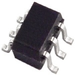
| 描述 | IC ADC 10BIT SRL 250KSPS SC70-6 |
| 产品分类 | |
| 品牌 | Analog Devices Inc |
| 数据手册 | |
| 产品图片 |
|
| 产品型号 | AD7910AKSZ-500RL7 |
| rohs | 无铅 / 符合限制有害物质指令(RoHS)规范要求 |
| 产品系列 | - |
| 位数 | 10 |
| 供应商器件封装 | SC-70-6 |
| 其它名称 | AD7910AKSZ-500RL7CT |
| 包装 | 带卷 (TR) |
| 安装类型 | 表面贴装 |
| 封装/外壳 | 6-TSSOP,SC-88,SOT-363 |
| 工作温度 | -40°C ~ 85°C |
| 数据接口 | DSP,MICROWIRE™,QSPI™,串行,SPI™ |
| 标准包装 | 1 |
| 特性 | - |
| 电压源 | 单电源 |
| 转换器数 | 1 |
| 输入数和类型 | 1 个单端,单极 |
| 配用 | /product-detail/zh/EVAL-AD7910CBZ/EVAL-AD7910CBZ-ND/1679970 |
| 采样率(每秒) | 250k |


- 商务部:美国ITC正式对集成电路等产品启动337调查
- 曝三星4nm工艺存在良率问题 高通将骁龙8 Gen1或转产台积电
- 太阳诱电将投资9.5亿元在常州建新厂生产MLCC 预计2023年完工
- 英特尔发布欧洲新工厂建设计划 深化IDM 2.0 战略
- 台积电先进制程称霸业界 有大客户加持明年业绩稳了
- 达到5530亿美元!SIA预计今年全球半导体销售额将创下新高
- 英特尔拟将自动驾驶子公司Mobileye上市 估值或超500亿美元
- 三星加码芯片和SET,合并消费电子和移动部门,撤换高东真等 CEO
- 三星电子宣布重大人事变动 还合并消费电子和移动部门
- 海关总署:前11个月进口集成电路产品价值2.52万亿元 增长14.8%


PDF Datasheet 数据手册内容提取
250 kSPS, 10-/12-Bit ADCs in 6-Lead SC70 AD7910/AD7920 FEATURES FUNCTIONAL BLOCK DIAGRAM Throughput rate: 250 kSPS VDD Specified for V of 2.35 V to 5.25 V DD Low power 3.6 mW typ at 250 kSPS with 3 V supplies 10-/12-BIT 12.5 mW typ at 250 kSPS with 5 V supplies VIN T/H APSPURCOCXEISMSAITVIEON Wide input bandwidth ADC 71 dB SNR at 100 kHz input frequency Flexible power/serial clock speed management No pipeline delays SCLK High speed serial interface CONTROL LOGIC SDATA SPI®-/QSPI™-/MICROWIRE™-/DSP-compatible CS Standby mode: 1 μA max AD7910/AD7920 6-lead SC70 package 8 -lead MSOP package GND 02976-001 Figure 1. APPLICATIONS Battery-powered systems Personal digital assistants Medical instruments Mobile communications Instrumentation and control systems Data acquisition systems High speed modems Optical sensors GENERAL DESCRIPTION PRODUCT HIGHLIGHTS The AD7910/AD79201 are, respectively, 10-bit and 12-bit, high 1. 10-/12-bit ADCs in SC70 and MSOP packages. speed, low power, successive approximation ADCs. The parts operate from a single 2.35 V to 5.25 V power supply and feature 2. Low power consumption. throughput rates up to 250 kSPS. The parts contain a low noise, 3. Flexible power/serial clock speed management. The wide bandwidth track-and-hold amplifier that can handle input conversion rate is determined by the serial clock, allowing frequencies in excess of 13 MHz. the conversion time to be reduced through the serial clock The conversion process and data acquisition are controlled speed increase. This allows the average power consumption using CS and the serial clock, allowing the devices to interface to be reduced when power-down mode is used while not converting. The part also features a power-down mode to with microprocessors or DSPs. The input signal is sampled on maximize power efficiency at lower throughput rates. the falling edge of CS and the conversion is initiated at this Current consumption is 1 μA maximum and 50 nA typically point. There are no pipeline delays associated with the part. when in power-down mode. The AD7910/AD7920 use advanced design techniques to 4. Reference derived from the power supply. achieve very low power dissipation at high throughput rates. 5. No pipeline delay. The parts feature a standard successive The reference for the part is taken internally from V . This DD approximation ADC with accurate control of the sampling allows the widest dynamic input range to the ADC. Thus, the instant via a CS input and once-off conversion control. analog input range for the part is 0 to V . The conversion rate DD is determined by the SCLK. 1 Protected by U.S. Patent No. 6,681,332. Rev. C Information furnished by Analog Devices is believed to be accurate and reliable. However, no responsibility is assumed by Analog Devices for its use, nor for any infringements of patents or other One Technology Way, P.O. Box 9106, Norwood, MA 02062-9106, U.S.A. rights of third parties that may result from its use. Specifications subject to change without notice. No license is granted by implication or otherwise under any patent or patent rights of Analog Devices. Tel: 781.329.4700 www.analog.com Trademarks and registered trademarks are the property of their respective owners. Fax: 781.461.3113 © 2005 Analog Devices, Inc. All rights reserved.
AD7910/AD7920 TABLE OF CONTENTS Features..............................................................................................1 ADC Transfer Function.............................................................14 Applications.......................................................................................1 Typical Connection Diagram...................................................14 Functional Block Diagram..............................................................1 Analog Input...............................................................................15 General Description.........................................................................1 Digital Inputs..............................................................................15 Product Highlights...........................................................................1 Modes of Operation.......................................................................16 Specifications.....................................................................................3 Normal Mode..............................................................................16 AD7910..........................................................................................3 Power-Down Mode....................................................................16 AD7920..........................................................................................4 Power-Up Time..........................................................................16 Timing Specifications..................................................................6 Power vs. Throughput Rate...........................................................18 Timing Examples..............................................................................7 Serial Interface................................................................................19 Timing Example 1........................................................................7 Microprocessor Interfacing...........................................................20 Timing Example 2........................................................................7 AD7910/AD7920 to TMS320C541 Interface.........................20 Absolute Maximum Ratings............................................................8 AD7910/AD7920 to ADSP-218x..............................................20 ESD Caution..................................................................................8 AD7910/AD7920 to DSP563xx Interface...............................21 Pin Configurations and Function Descriptions...........................9 Application Hints...........................................................................22 Typical Performance Characteristics...........................................10 Grounding and Layout..............................................................22 Terminology....................................................................................12 Evaluating Performance............................................................22 Circuit Information........................................................................13 Outline Dimensions.......................................................................23 Converter Operation......................................................................14 Ordering Guide..........................................................................24 REVISION HISTORY 9/05—Rev. B to Rev. C 8/03—Rev. 0 to Rev. A Updated Formatting..........................................................Universal Changes to Ordering Guide.............................................................6 Updated Outline Dimensions.......................................................23 Changes to Evaluating the AD7910/AD7920 Performance Changes to Ordering Guide..........................................................24 Section..............................................................................................18 Updated Outline Dimensions......................................................19 3/04—Rev. A to Rev. B Added U.S. Patent Number............................................................1 Changes to Note 5............................................................................2 Changes to Note 6 of AD7920 Specifications...............................4 Changes to Note 1 of Timing Specifications................................4 Changes to Absolute Maximum Ratings......................................6 Changes to Ordering Guide............................................................6 Rev. C | Page 2 of 24
AD7910/AD7920 SPECIFICATIONS AD7910 V = 2.35 V to 5.25 V, f = 5 MHz, f = 250 kSPS, T = T to T , unless otherwise noted. DD SCLK SAMPLE A MIN MAX Table 1. Parameter1 A Grade1, 2 Unit Test Conditions/Comments DYNAMIC PERFORMANCE f = 100 kHz sine wave IN Signal-to-Noise + Distortion (SINAD)3 61 dB min Total Harmonic Distortion (THD)3 −72 dB max Peak Harmonic or Spurious Noise (SFDR)3 −73 dB max Intermodulation Distortion (IMD)3 Second-Order Terms −82 dB typ fa = 100.73 kHz, fb = 90.7 kHz Third-Order Terms −82 dB typ fa = 100.73 kHz, fb = 90.7 kHz Aperture Delay 10 ns typ Aperture Jitter 30 ps typ Full Power Bandwidth 13.5 MHz typ @ 3 dB 2 MHz typ @ 0.1 dB DC ACCURACY Resolution 10 Bits Integral Nonlinearity ±0.5 LSB max Differential Nonlinearity ±0.5 LSB max Guaranteed no missed codes to 10 bits Offset Error3, 4 ±1 LSB max Gain Error3, 4 ±1 LSB max Total Unadjusted Error (TUE)3, 4 ±1.2 LSB max ANALOG INPUT Input Voltage Ranges 0 to V V DD DC Leakage Current ±0.5 μA max Input Capacitance 20 pF typ Track-and-hold in track, 6 pF typ when in hold LOGIC INPUTS Input High Voltage, V 2.4 V min INH Input Low Voltage, V 0.8 V max V = 5 V INL DD 0.4 V max V = 3 V DD Input Current, I , SCLK Pin ± 0.5 μA max Typically 10 nA, V = 0 V or V IN IN DD Input Current, I , CS Pin ± 10 nA typ IN Input Capacitance, C 5 5 pF max IN LOGIC OUTPUTS Output High Voltage, V V − 0.2 V min I = 200 μA, V = 2.35 V to 5.25 V OH DD SOURCE DD Output Low Voltage, V 0.4 V max I = 200 μA OL SINK Floating-State Leakage Current ±1 μA max Floating-State Output Capacitance5 5 pF max Output Coding Straight (natural) binary CONVERSION RATE Conversion Time 2.8 μs max 14 SCLK cycles with SCLK at 5 MHz Track-and-Hold Acquisition Time3 250 ns max Throughput Rate 250 kSPS max POWER REQUIREMENTS V 2.35/5.25 V min/max DD I Digital I/Ps = 0 V or V DD DD Normal Mode (Static) 2.5 mA typ V = 4.75 V to 5.25 V, SCLK on or off DD 1.2 mA typ V = 2.35 V to 3.6 V, SCLK on or off DD Normal Mode (Operational) 3 mA max V = 4.75 V to 5.25 V, f = 250 kSPS DD SAMPLE 1.4 mA max V = 2.35 V to 3.6 V, f = 250 kSPS DD SAMPLE Full Power-Down Mode 1 μA max Typically 50 nA Rev. C | Page 3 of 24
AD7910/AD7920 Parameter1 A Grade1, 2 Unit Test Conditions/Comments Power Dissipation6 Normal Mode (Operational) 15 mW max V = 5 V, f = 250 kSPS DD SAMPLE 4.2 mW max V = 3 V, f = 250 kSPS DD SAMPLE Full Power-Down 5 μW max V = 5 V DD 3 μW max V = 3 V DD 1 Temperature range from −40°C to +85°C. 2 Operational from VDD = 2.0 V, with input high voltage (VINH) 1.8 V min. 3 See the Terminology section. 4 SC70 values guaranteed by characterization. 5 Guaranteed by characterization. 6 See the Power vs. Throughput Rate section. AD7920 V = 2.35 V to 5.25 V, f = 5 MHz, f = 250 kSPS, T = T to T , unless otherwise noted. DD SCLK SAMPLE A MIN MAX Table 2. Parameter1 A Grade 1, 2 B Grade1, 2 Unit Test Conditions/Comments DYNAMIC PERFORMANCE f = 100 kHz sine wave IN Signal-to-Noise + Distortion (SINAD)3 70 70 dB min V = 2.35 V to 3.6 V, T = 25°C DD A 69 69 dB min V = 2.4 V to 3.6 V DD 71.5 71.5 dB typ V = 2.35 V to 3.6 V DD 69 69 dB min V = 4.75 V to 5.25 V, T = 25°C DD A 68 68 dB min V = 4.75 V to 5.25 V DD Signal-to-Noise Ratio (SNR)3 71 71 dB min V = 2.35 V to 3.6 V, T = 25°C DD A 70 70 dB min V = 2.4 V to 3.6 V DD 70 70 dB min V = 4.75 V to 5.25 V, T = 25°C DD A 69 69 dB min V = 4.75 V to 5.25 V DD Total Harmonic Distortion (THD)3 −80 −80 dB typ Peak Harmonic or Spurious Noise (SFDR)3 −82 −82 dB typ Intermodulation Distortion (IMD)3 Second-Order Terms −84 −84 dB typ fa = 100.73 kHz, fb = 90.72 kHz Third-Order Terms −84 −84 dB typ fa = 100.73 kHz, fb = 90.72 kHz Aperture Delay 10 10 ns typ Aperture Jitter 30 30 ps typ Full Power Bandwidth 13.5 13.5 MHz typ @ 3 dB 2 2 MHz typ @ 0.1 dB DC ACCURACY B Grade4 Resolution 12 12 Bits Integral Nonlinearity3 ±1.5 LSB max ± 0.75 LSB typ Differential Nonlinearity −0.9/+1.5 LSB max Guaranteed no missed codes to 12 bits ±0.75 LSB typ Offset Error3, 5 ±1.5 LSB max ±1.5 ±0.2 LSB typ Gain Error3, 5 ±1.5 LSB max ±1.5 ±0.5 LSB typ Total Unadjusted Error (TUE)3, 5 ±2 LSB max ANALOG INPUT Input Voltage Ranges 0 to V 0 to V V DD DD DC Leakage Current ±0.5 ±0.5 μA max Input Capacitance 20 20 pF typ Track-and-hold in track, 6 pF typ when in hold Rev. C | Page 4 of 24
AD7910/AD7920 Parameter1 A Grade 1, 2 B Grade1, 2 Unit Test Conditions/Comments LOGIC INPUTS Input High Voltage, V 2.4 2.4 V min INH 1.8 1.8 V min V = 2.35 V DD Input Low Voltage, V 0.8 0.8 V max V = 3.6 V to 5.25 V INL DD 0.4 0.4 V max V = 2.35 V to 3.6 V DD Input Current, I , SCLK Pin ±0.5 ±0.5 μA max Typically 10 nA, V = 0 V or V IN IN DD Input Current, I , CS Pin ±10 ±10 nA typ IN Input Capacitance, C 6 5 5 pF max IN LOGIC OUTPUTS Output High Voltage, V V − 0.2 V − 0.2 V min I = 200 μA, V = 2.35 V to 5.25 V OH DD DD SOURCE DD Output Low Voltage, V 0.4 0.4 V max I = 200 μA OL SINK Floating-State Leakage Current ±1 ±1 μA max Floating-State Output Capacitance6 5 5 pF max Output Coding Straight (natural) binary CONVERSION RATE Conversion Time 3.2 3.2 μs max 16 SCLK cycles with SCLK at 5 MHz Track-and-Hold Acquisition Time3 250 250 ns max Throughput Rate 250 250 kSPS max See the Serial Interface section POWER REQUIREMENTS V 2.35/5.25 2.35/5.25 V min/max DD I Digital I/Ps = 0 V or V DD DD Normal Mode (Static) 2.5 2.5 mA typ V = 4.75 V to 5.25 V, SCLK on or off DD 1.2 1.2 mA typ V = 2.35 V to 3.6 V, SCLK on or off DD Normal Mode (Operational) 3 3 mA max V = 4.75 V to 5.25 V, f = 250 kSPS DD SAMPLE 1.4 1.4 mA max V = 2.35 V to 3.6 V, f = 250 kSPS DD SAMPLE Full Power-Down Mode 1 1 μA max Typically 50 nA Power Dissipation7 Normal Mode (Operational) 15 15 mW max V = 5 V, f = 250 kSPS DD SAMPLE 4.2 4.2 mW max V = 3 V, f = 250 kSPS DD SAMPLE Full Power-Down 5 5 μW max V = 5 V DD 3 3 μW max V = 3 V DD 1 Temperature range from −40°C to +85°C. 2 Operational from VDD = 2.0 V, with input low voltage (VINL) 0.35 V max. 3 See the Terminology section. 4 B Grade, maximum specifications apply as typical figures when VDD = 4.75 V to 5.25 V. 5 SC70 values guaranteed by characterization. 6 Guaranteed by characterization. 7 See the Power vs. Throughput Rate section. Rev. C | Page 5 of 24
AD7910/AD7920 TIMING SPECIFICATIONS V = 2.35 V to 5.25 V, T = T to T , unless otherwise noted. DD A MIN MAX Table 3. AD7910/AD7920 Parameter1 Limit at T , T Unit Description MIN MAX f 2 10 kHz min3 SCLK 5 MHz max t 14 × t AD7910 CONVERT SCLK 16 × t AD7920 SCLK t 50 ns min Minimum quiet time required between bus relinquish and start of next QUIET conversion t 10 ns min Minimum CS pulse width 1 t 10 ns min CS to SCLK setup time 2 t 4 22 ns max Delay from CS until SDATA three-state disabled 3 t 40 ns max Data access time after SCLK falling edge 4 t 0.4 × t ns min SCLK low pulse width 5 SCLK t 0.4 × t ns min SCLK high pulse width 6 SCLK t 5, 6 SCLK to data valid hold time 7 10 ns min V ≤ 3.3 V DD 9.5 ns min 3.3 V < V ≤ 3.6 V DD 7 ns min V > 3.6 V DD t6, 7 36 ns max SCLK falling edge to SDATA three-state 8 See Note 7 ns min SCLK falling edge to SDATA three-state t 8 1 μs max Power-up time from full power-down POWER-UP 1 Guaranteed by characterization. All input signals are specified with tr = tf = 5 ns (10% to 90% of VDD) and timed from a voltage level of 1.6 V. 2 Mark/Space ratio for the SCLK input is 40/60 to 60/40. 3 Minimum fSCLK at which specifications are guaranteed. 4 Measured with the load circuit of Figure 2 and defined as the time required for the output to cross 0.8 V or 1.8 V when VDD = 2.35 V and 0.8 V or 2.0 V for VDD > 2.35 V. 5 Measured with a 50 pF load capacitor. 6 t8 is derived from the measured time taken by the data outputs to change 0.5 V when loaded with the circuit of Figure 2. The measured number is then extrapolated back to remove the effects of charging or discharging the 50 pF capacitor. This means that the time, t8, shown in the Timing Specifications is the true bus relinquish time of the part and is independent of the bus loading. 7 T7 values apply to t8 minimum values also. 8 See Power-Up Time section. 200μA IOL TO OUTPUT 1.6V PIN CL 50pF 200μA IOH 02976-002 Figure 2. Load Circuit for Digital Output Timing Specifications Rev. C | Page 6 of 24
AD7910/AD7920 TIMING EXAMPLES Figure 3 and Figure 4 show some of the timing parameters from TIMING EXAMPLE 2 Table 3. The AD7920 can also operate with slower clock frequencies. From Figure 4, having f = 3.4 MHz and a throughput rate of TIMING EXAMPLE 1 SCLK 150 kSPS gives a cycle time of t + 12.5(1/f ) + t = 6.66 μs. 2 SCLK ACQ From Figure 4, having f = 5 MHz and a throughput rate of SCLK With t = 10 ns min, this leaves t to be 2.97 μs. This 2.97 μs 2 ACQ 250 kSPS gives a cycle time of t + 12.5(1/f ) + t = 4 μs. 2 SCLK ACQ satisfies the requirement of 250 ns for t . From Figure 4, t ACQ ACQ With t = 10 ns min, this leaves t to be 1.49 μs. This 1.49 μs 2 ACQ comprises 2.5(1/f ) + t + t , t = 36 ns max. This allows a SCLK 8 QUIET 8 satisfies the requirement of 250 ns for t . From Figure 4, t ACQ ACQ value of 2.19 μs for t , satisfying the minimum requirement QUIET comprises 2.5(1/f ) + t + t , where t = 36 ns max. This SCLK 8 QUIET 8 of 50 ns. As in this example and with other slower clock values, allows a value of 954 ns for t , satisfying the minimum QUIET the signal may already be acquired before the conversion is requirement of 50 ns. complete, but it is still necessary to leave 50 ns minimum t QUIET between conversions. In this example, the signal should be fully acquired at approximately Point C in Figure 4. t 1 CS t CONVERT t2 t6 B SCLK 1 2 3 4 5 13 14 15 16 t5 t8 t3 t4 t7 tQUIET SDATA TSHTRAETEE- Z ZE4R LOEADIZNEGR ZOEROSZERO DB11 DB10 DB2 DB1 DB0 THREE-STATE 02976-003 Figure 3. AD7920 Serial Interface Timing Diagram CS t CONVERT t2 B C SCLK 1 2 3 4 5 13 14 15 16 t 8 t QUIET 12.5(1/fSCLK) tACQ 1/THROUGHPUT 02976-004 Figure 4. Serial Interface Timing Example Rev. C | Page 7 of 24
AD7910/AD7920 ABSOLUTE MAXIMUM RATINGS T = 25°C, unless otherwise noted. A Table 4. Stresses above those listed under Absolute Maximum Ratings may cause permanent damage to the device. This is a stress Parameter Rating rating only; functional operation of the device at these or any V to GND −0.3 V to +7 V DD other conditions above those indicated in the operational Analog Input Voltage to GND −0.3 V to V + 0.3 V DD section of this specification is not implied. Exposure to absolute Digital Input Voltage to GND −0.3 V to +7 V maximum rating conditions for extended periods may affect Digital Output Voltage to GND −0.3 V to V + 0.3 V DD device reliability. Input Current to Any Pin Except Supplies1 ± 10 mA Operating Temperature Range Commercial (A, B Grade) −40°C to +85°C Storage Temperature Range −65°C to +150°C Junction Temperature 150°C MSOP Package θJA Thermal Impedance 205.9°C/W θ Thermal Impedance 43.74°C/W JC SC70 Package θ Thermal Impedance 340.2°C/W JA θ Thermal Impedance 228.9°C/W JC Lead Temperature, Soldering Reflow (10 sec to 30 sec) 235 (0/+5)°C ESD 3.5 kV 1 Transient currents of up to 100 mA will not cause SCR latch-up. ESD CAUTION ESD (electrostatic discharge) sensitive device. Electrostatic charges as high as 4000 V readily accumulate on the human body and test equipment and can discharge without detection. Although this product features proprietary ESD protection circuitry, permanent damage may occur on devices subjected to high energy electrostatic discharges. Therefore, proper ESD precautions are recommended to avoid performance degradation or loss of functionality. Rev. C | Page 8 of 24
AD7910/AD7920 PIN CONFIGURATIONS AND FUNCTION DESCRIPTIONS VDD 1 6 CS VDD 1 AD7910/ 8 VIN AD7910/ SDATA 2 AD7920 7 GND GND 2 AD7920 5 SDATA CS 3 TOP VIEW 6 SCLK TOP VIEW (Not to Scale) VIN 3 (Not to Scale) 4 SCLK 02976-005 NC 4NC = NO CONNECT5 NC 02976-006 Figure 5. 6-Lead SC70 Pin Configuration Figure 6. 8-Lead MSOP Pin Configuration Table 5. Pin Function Descriptions Pin No. Pin No. 6-Lead 8-Lead SC70 MSOP Mnemonic Description 6 3 CS Chip Select. Active low logic input. This input provides the dual function of initiating conversions on the AD7910/AD7920 and framing the serial data transfer. 1 1 V Power Supply Input. The V range for the AD7910/AD7920 is from 2.35 V to 5.25 V. DD DD 2 7 GND Analog Ground. Ground reference point for all circuitry on the AD7910/AD7920. All analog input signals should be referred to this GND voltage. 3 8 V Analog Input. Single-ended analog input channel. The input range is 0 to V . IN DD 5 2 SDATA Data Out. Logic output. The conversion result from the AD7910/AD7920 is provided on this output as a serial data stream. The bits are clocked out on the falling edge of the SCLK input. The data stream from the AD7920 consists of four leading zeros followed by the 12 bits of conversion data, which is provided MSB first. The data stream from the AD7910 consists of four leading zeros followed by the 10 bits of conversion data followed by two trailing zeros, which is also provided MSB first. 4 6 SCLK Serial Clock. Logic input. SCLK provides the serial clock for accessing data from the part. This clock input is also used as the clock source for the AD7910/AD7920 conversion process. N/A 4, 5 NC No Connect. Rev. C | Page 9 of 24
AD7910/AD7920 TYPICAL PERFORMANCE CHARACTERISTICS Figure 7 and Figure 8 show a typical FFT plot for the AD7920 and Figure 12 shows a graph of the total harmonic distortion vs. analog AD7910, respectively, at a 250 kSPS sampling rate and a 100 kHz input frequency for different source impedances when using a input frequency. supply voltage of 3.6 V and sampling at a rate of 250 kSPS. See the Analog Input section. Figure 9 shows the signal-to-(noise + distortion) ratio performance vs. input frequency for various supply voltages while sampling at Figure 13 shows a graph of the total harmonic distortion vs. 250 kSPS with an SCLK frequency of 5 MHz for the AD7920. analog input signal frequency for various supply voltages while sampling at 250 kSPS with an SCLK frequency of 5 MHz. Figure 10 and Figure 11 show typical INL and DNL performance for the AD7920. –5 –71.0 8192 POINT FFT –15 fVfSINDA D=M =P1 L02E0. 7k=VH 2z50kSPS –71.5 VDD = 5.25V SINAD = 72.05dB THD =–82.87dB –35 SFDR =–87.24dB R (dB) –55 AD (dB)–72.0 VDD = 4.75V VDD = 3.6V VDD = 2.7V N N S SI–72.5 –75 VDD= 2.35V –73.0 –95 –1150 25 FR5E0QUENCY (k7H5z) 100 12502976-007 –73.510 FREQUE1N00CY (kHz) 100002976-009 Figure 7. AD7920 Dynamic Performance at 250 kSPS Figure 9. AD7920 SINAD vs. Input Frequency at 250 kSPS 15 1.0 8192 POINT FFT VDD = 2.35V VDD = 2.35V 0.8 TEMP = 25°C –5 fSAMPLE = 250kSPS fSAMPLE = 250kSPS fIN = 100kHz 0.6 SINAD = 61.67dB THD =–79.59dB 0.4 –25 SFDR =–82.93dB B) dB) R (LS 0.2 SNR ( –45 L ERRO –0.20 –65 N I –0.4 –0.6 –85 –0.8 –1050 25 FR5E0QUENCY (k7H5z) 100 12502976-008 –1.00 512 1024 1536 C2O04D8E 2560 3072 3584 409602976-010 Figure 8. AD7910 Dynamic Performance at 250 kSPS Figure 10. AD7920 INL Performance Rev. C | Page 10 of 24
AD7910/AD7920 1.0 –65 VDD = 2.35V 0.8 TEMP = 25°C fSAMPLE = 250kSPS 0.6 –70 0.4 B) ROR (LS 0.20 D (dB) –75 VDD = 2.35V R H L E –0.2 T –80 N D –0.4 VDD = 4.75V –0.6 –85 VDD = 3.6V –0.8 VDD = 5.25V VDD = 2.7V –1.00 512 1024 1536 C2O04D8E 2560 3072 3584 409602976-011 –9010 INPUT FRE1Q0U0ENCY (kHz) 100002976-013 Figure 11. AD7920 DNL Performance Figure 13. THD vs. Analog Input Frequency for Various Supply Voltages –10 VDD = 3.6V –20 –30 –40 B) RIN = 10kΩ d D ( –50 H T –60 –70 RIN = 1kΩ RIN = 130Ω RIN = 13Ω –80 RIN = 0Ω –9010 INPUT FRE1Q0U0ENCY (kHz) 100002976-012 Figure 12. THD vs. Analog Input Frequency for Various Source Impedances Rev. C | Page 11 of 24
AD7910/AD7920 TERMINOLOGY Integral Nonlinearity Total Unadjusted Error The maximum deviation from a straight line passing through A comprehensive specification that includes gain error, linearity the endpoints of the ADC transfer function. For the AD7920 error, and offset error. and AD7910, the endpoints of the transfer function are zero Total Harmonic Distortion (THD) scale, a point 1 LSB below the first code transition, and full Total harmonic distortion is the ratio of the rms sum of scale, a point 1 LSB above the last code transition. harmonics to the fundamental. It is defined as: Differential Nonlinearity V2+V2+V2+V2+V2 The difference between the measured and the ideal 1 LSB THD(dB)=20log 2 3 4 5 6 V change between any two adjacent codes in the ADC. 1 where: Offset Error V is the rms amplitude of the fundamental. The deviation of the first code transition (00 . . . 000) to (00 . . . 001) 1 from the ideal, that is, GND + 1 LSB. V, V, V, V, and V are the rms amplitudes of the second 2 3 4 5 6 through the sixth harmonics. Gain Error The deviation of the last code transition (111 . . . 110) to Peak Harmonic or Spurious Noise (111 . . . 111) from the ideal, that is, VREF − 1 LSB after the offset Peak harmonic or spurious noise is the ratio of the rms value of error has been adjusted out. the next largest component in the ADC output spectrum (up to f/2 and excluding dc) to the rms value of the fundamental. S Track-and-Hold Acquisition Time Normally, the value of this specification is determined by the The track-and-hold amplifier returns to track mode at the end largest harmonic in the spectrum, but for ADCs whose of conversion. Track-and-hold acquisition time is the time harmonics are buried in the noise floor, it is a noise peak. required for the output of the track-and-hold amplifier to reach its final value, within ±0.5 LSB, after the end of conversion. See Intermodulation Distortion the Serial Interface section for more details. With inputs consisting of sine waves at two frequencies, fa and fb, any active device with nonlinearities creates distortion products Signal-to-(Noise + Distortion) Ratio at sum and difference frequencies of mfa ± nfb where m, n = 0, 1, The measured ratio of signal-to-(noise + distortion) at the output 2, 3, and so on. Intermodulation distortion terms are those for of the A/D converter. The signal is the rms amplitude of the which neither m nor n are equal to zero. For example, the second- fundamental. Noise is the sum of all nonfundamental signals up order terms include (fa + fb) and (fa − fb), while the third-order to half the sampling frequency (f/2), excluding dc. The ratio is S terms include (2fa + fb), (2fa − fb), (fa + 2fb), and (fa − 2fb). dependent on the number of quantization levels in the digiti- zation process. The more levels, the smaller the quantization The AD7910/AD7920 are tested using the CCIF standard, where noise. The theoretical signal-to-(noise + distortion) ratio for an two input frequencies are used (see fa and fb in the Specifications ideal N-bit converter with a sine wave input is given by: page). In this case, the second-order terms are usually distanced in frequency from the original sine waves, while the third-order terms Signal-to-(Noise + Distortion) = (6.02N + 1.76) dB are usually at a frequency close to the input frequencies. As a result, Thus, for a 12-bit converter this is 74 dB, and for a 10-bit the second- and third-order terms are specified separately. The converter this is 62 dB. calculation of the intermodulation distortion is as per the THD specification, the ratio of the rms sum of the individual distortion products to the rms amplitude of the sum of the fundamentals, expressed in dB. Rev. C | Page 12 of 24
AD7910/AD7920 CIRCUIT INFORMATION The AD7910/AD7920 are fast, micropower, 10-bit/12-bit, The serial clock input accesses data from the part but also single-supply A/D converters, respectively. The parts can be provides the clock source for the successive approximation A/D operated from a 2.35 V to 5.25 V supply. When operated from converter. The analog input range is 0 V to V . An external DD either a 5 V supply or a 3 V supply, the AD7910/AD7920 are reference is not required for the ADC and there is no reference capable of throughput rates of 250 kSPS when provided with a on-chip. The reference for the AD7910/AD7920 is derived from 5 MHz clock. the power supply and thus gives the widest dynamic input range. The AD7910/AD7920 provide the user with an on-chip track- and-hold, A/D converter, and a serial interface housed in a tiny The AD7910/AD7920 also feature a power-down option to 6-lead SC70 package or 8-lead MSOP package, which offers the allow power saving between conversions. The power-down user considerable space saving advantages over alternative feature is implemented across the standard serial interface, as solutions. described in the Modes of Operation section. Rev. C | Page 13 of 24
AD7910/AD7920 CONVERTER OPERATION The AD7910/AD7920 are successive approximation analog-to- digital converters based around a charge redistribution DAC. 111...111 Figure 14 and Figure 15 show simplified schematics of the 111...110 ADC. Figure 14 shows the ADC during its acquisition phase. When SW2 is closed and SW1 is in Position A, the comparator ODE 111...000 1LSB = VDD/1024 (AD7910) is held in a balanced condition, and the sampling capacitor C C 011...111 1LSB = VDD/4096 (AD7920) D A acquires the signal on V . IN 000...010 000...001 REDCISHTDARARICBGUETION 000...000 0V 1LSB ANALOG INPUT +VDD– 1LSB 02976-016 SAMPLING Figure 16. Transfer Characteristic CAPACITOR A VIN SW1 CONTROL TYPICAL CONNECTION DIAGRAM LOGIC B ACQUISITION PHASE SW2 Figure 17 shows a typical connection diagram for the AD7910/ AGND VDD/2 COMPARATOR 02976-014 AshDou79ld2 0b.e V wReElFl ids etcaokuenp liendt.e Trnhailsl yp rforovmid eVs DaDn a annda,l oasg siuncphu,t V raDnD ge of Figure 14. ADC Acquisition Phase 0 V to V . The conversion result is output in a 16-bit word with DD When the ADC starts a conversion (see Figure 15), SW2 opens four leading zeros followed by the MSB of the 12-bit or 10-bit and SW1 moves to Position B, causing the comparator to become result. Two trailing zeros follow the 10-bit result from the unbalanced. The control logic and charge redistribution DAC are AD7910. used to add and subtract fixed amounts of charge from the Alternatively, because the supply current required by the sampling capacitor to bring the comparator back into a balanced AD7910/AD7920 is so low, a precision reference can be used as condition. When the comparator is rebalanced, the conversion is the supply source to the AD7910/AD7920. An REF19x voltage complete. The control logic generates the ADC output code. reference (REF195 for 5 V or REF193 for 3 V) can be used to Figure 16 shows the ADC transfer function. supply the required voltage to the ADC (see Figure 17). This configuration is especially useful if the power supply is quite CHARGE REDISTRIBUTION noisy or if the system supply voltages are at a value other than DAC 5 V or 3 V (for example, 15 V). The REF19x outputs a steady SAMPLING A CAPACITOR voltage to the AD7910/AD7920. If the low dropout REF193 is VIN SW1 CONTROL used, the current it needs to supply to the AD7910/AD7920 is LOGIC B CONVERSION SW2 PHASE typically 1.2 mA. When the ADC is converting at a rate of AGND VDD/2 COMPARATOR 02976-015 2th5e0 AkSDP7S9,1 t0h/eA RDE7F912903. Tneheed lso taod sruepgpullya taio mn aoxfi mthue mRE oFf 119.43 mis A to Figure 15. ADC Conversion Phase typically 10 ppm/mA (REF193, V = 5 V), which results in an S error of 14 ppm (42 μV) for the 1.4 mA drawn from it. This ADC TRANSFER FUNCTION corresponds to a 0.057 LSB error for the AD7920 with V = DD The output coding of the AD7910/AD7920 is straight binary. 3 V from the REF193 and a 0.014 LSB error for the AD7910. The designed code transitions occur at the successive integer For applications where power consumption is of concern, the LSB values, that is, 1 LSB, 2 LSBs, and so on. The LSB size is power-down mode of the ADC and the sleep mode of the VDD/4096 for the AD7920 and VDD/1024 for the AD7910. The REF19x reference should be used to improve power ideal transfer characteristic for the AD7910/AD7920 is shown performance. See the Modes of Operation section. in Figure 16. Rev. C | Page 14 of 24
AD7910/AD7920 3V REF193 5V SUPPLY 1.2mA 1μF 0.1μF TANT 10μF 0.1μF 680nF VDD VDD AD7910/ D1 R1 2C0p2F AD7920 VIN 0V TION PVUDTD VIN SDSCALTKA μC/μP 6CpF1 D2 GND CS CTROANCVKE RPSHIAOSNE P—HSAWSEIT—CHSW CILTOCSHE ODPEN02976-018 INTSEERRFIAALCE 02976-017 Figure 17. REF193 as Power Supply Figure 18. Equivalent Analog Input Circuit Table 6 provides typical performance data with various Table 7 provides some typical performance data with various op references used as a V source for a 100 kHz input tone at amps used as the input buffer for a 100 kHz input tone at room DD room temperature, under the same setup conditions. temperature, under the same setup conditions. Table 6. AD7920 Typical Performance for Various Voltage Table 7. AD7920 Typical Performance for Various Input References IC Buffers, VDD = 3 V Reference Tied to V AD7920 SNR Performance (dB) Op Amp in the Input Buffer AD7920 SNR Performance (dB) DD AD780 @ 3 V 72.65 AD711 72.3 REF193 72.35 AD797 72.5 AD780 @ 2.5 V 72.5 AD845 71.4 REF192 72.2 When no amplifier is used to drive the analog input, the source REF43 72.6 impedance should be limited to low values. The maximum source impedance depends on the amount of total harmonic ANALOG INPUT distortion (THD) that can be tolerated. The THD increases as Figure 18 shows an equivalent circuit of the analog input the source impedance increases, and performance degrades (see structure of the AD7910/AD7920. The two diodes, D1 and D2, Figure 12). provide ESD protection for the analog input. Care must be DIGITAL INPUTS taken to ensure that the analog input signal never exceeds the supply rails by more than 300 mV. This causes these diodes to The digital inputs applied to the AD7910/AD7920 are not limited become forward biased and start conducting current into the by the maximum ratings that limit the analog input. Instead, the substrate. The maximum current these diodes can conduct digital inputs applied can go to 7 V and are not restricted by the without causing irreversible damage to the parties is 10 mA. V + 0.3 V limit as on the analog input. For example, if the DD Capacitor C1 in Figure 18 is typically about 6 pF and can be AD7910/AD7920 were operated with a V of 3 V, then 5 V logic DD attributed primarily to pin capacitance. Resistor R1 is a lumped levels could be used on the digital inputs. However, it is important component made up of the on resistance of a switch. This to note that the data output on SDATA still have 3 V logic levels resistor is typically about 100 Ω. Capacitor C2 is the ADC when V = 3 V. Another advantage of SCLK and CS not being DD sampling capacitor and has a capacitance of 20 pF typically. For restricted by the V + 0.3 V limit is that power supply DD ac applications, removing high frequency components from the sequencing issues are avoided. If CS or SCLK is applied before analog input signal is recommended by use of a band-pass filter V , there is no risk of latch-up as there would be on the analog DD on the relevant analog input pin. In applications where inputs if a signal greater than 0.3 V were applied prior to V . DD harmonic distortion and signal-to-noise ratio are critical, the analog input should be driven from a low impedance source. Large source impedances significantly affect the ac performance of the ADC. This can necessitate the use of an input buffer amplifier. The choice of the op amp is a function of the particular application. Rev. C | Page 15 of 24
AD7910/AD7920 MODES OF OPERATION The mode of operation of the AD7910/AD7920 is selected by To enter power-down mode, the conversion process must be controlling the logic state of the CS signal during a conversion. interrupted by bringing CS high anywhere after the second There are two possible modes of operation, normal mode and falling edge of SCLK, and before the tenth falling edge of SCLK, power-down mode. The point at which CS is pulled high after as shown in Figure 20. Once CS is brought high in this window the conversion is initiated determines whether the of SCLKs, the part enters power-down mode, the conversion AD7910/AD7920 enters power-down mode. Similarly, if the that was initiated by the falling edge of CS is terminated, and device is already in power-down mode, CS can control whether SDATA goes back into three-state. If CS is brought high before it returns to normal operation or remains in power-down the second SCLK falling edge, the part remains in normal mode mode. These modes of operation are designed to provide and does not power down. This avoids accidental power-down flexible power management options. These options can be due to glitches on the CS line. chosen to optimize the power dissipation/throughput rate ratio for different application requirements. To exit this mode of operation and power up the AD7910/ AD7920 again, a dummy conversion is performed. On the falling NORMAL MODE edge of CS, the device begins to power up, and continues to This mode is intended for fastest throughput rate performance power up as long as CS is held low until after the falling edge of because the user does not have to worry about any power-up the tenth SCLK. The device is fully powered up once 16 SCLKs times; the AD7910/AD7920 remains fully powered all the time. have elapsed and valid data results from the next conversion, as Figure 19 shows the general diagram of the operation of the shown in Figure 21. If CS is brought high before the tenth SCLK AD7910/AD7920 in this mode. falling edge, the AD7910/AD7920 goes back into power-down mode again. This avoids accidental power-up due to glitches on The conversion is initiated on the falling edge of CS as the CS line or an inadvertent burst of eight SCLK cycles while CS described in the Serial Interface section. To ensure that the part is low. Although the device can begin to power up on the falling remains fully powered up at all times, CS must remain low until edge of CS, it powers down again on the rising edge of CS as long at least 10 SCLK falling edges have elapsed after the falling edge as it occurs before the tenth SCLK falling edge. of CS. If CS is brought high any time after the tenth SCLK falling edge but before the end of the t , then the part POWER-UP TIME CONVERT remains powered up but the conversion is terminated and The power-up time of the AD7910/AD7920 is 1 μs, which SDATA goes back into three-state. means that one dummy cycle is always sufficient to allow the device to power up. Once the dummy cycle is complete, the For the AD7920, 16 serial clock cycles are required to complete ADC fully powered up and the input signal acquired properly. the conversion and access the complete conversion result. For The quiet time, t , must still be allowed from the point the AD7910, a minimum of 14 serial clock cycles is required to QUIET where the bus goes back into three-state after the dummy complete the conversion and access the complete conversion conversion, to the next falling edge of CS. result. When powering up from the power-down mode with a dummy CS can idle high until the next conversion or can idle low until cycle, as in Figure 21, the track-and-hold that was in hold mode CS returns high sometime prior to the next conversion, while the part was powered down returns to track mode after effectively idling CS low. the first SCLK edge the part receives after the falling edge of CS. Once a data transfer is complete (SDATA has returned to three- This is shown as Point A in Figure 21. Although at any SCLK state), another conversion can be initiated after the quiet time, frequency one dummy cycle is sufficient to power up the device tQUIET, has elapsed by bringing CS low again. and acquire VIN, it does not necessarily mean that a full dummy cycle of 16 SCLKs must always elapse to power up the device POWER-DOWN MODE and fully acquire V ; 1 μs is sufficient to power the device up IN This mode is intended for use in applications where slower and acquire the input signal. Therefore, if a 5 MHz SCLK throughput rates are required; either the ADC is powered down frequency is applied to the ADC, the cycle time is 3.2 μs. In one between conversions, or a series of conversions can be dummy cycle, 3.2 μs, the part powers up and VIN is fully performed at a high throughput rate and the ADC is powered acquired. However, after 1 μs with a 5 MHz SCLK, only five down for a relatively long duration between these bursts of SCLK cycles have elapsed. At this stage, the ADC is fully several conversions. When the AD7910/AD7920 is in power- powered up and the signal is acquired. In this case, the CS can down mode, all analog circuitry is powered down. be brought high after the tenth SCLK falling edge and brought low again after a time, t , to initiate the conversion. QUIET Rev. C | Page 16 of 24
AD7910/AD7920 AD7910/AD7920 CS 1 10 12 14 16 SCLK SDATA VALID DATA 02976-019 Figure 19. Normal Mode Operation CS 1 2 10 12 14 16 SCLK SDATA THREE-STATE 02976-020 Figure 20. Entering Power-Down Mode THE PART THE PART IS FULLY BEGINS TO POWERED UP WITH POWER UP VIN FULLY ACQUIRED CS A 1 10 12 14 16 1 16 SCLK SDATA INVALID DATA VALID DATA 02976-021 Figure 21. Exiting Power-Down Mode When power supplies are first applied to the AD7910/AD7920, the Instead, the dummy cycle can occur directly after power is ADC can power up in either power-down mode or in normal supplied to the ADC. If the first valid conversion is performed mode. Because of this, it is best to allow a dummy cycle to elapse to directly after the dummy conversion, care must be taken to ensure the part is fully powered up before attempting a valid ensure that adequate acquisition time is allowed. As mentioned conversion. Likewise, if the intention is to keep the part in power- earlier, when powering up from the power-down mode, the part down mode while not in use and the user wishes the part to power returns to track upon the first SCLK edge applied after the up in power-down mode, the dummy cycle can be used to ensure falling edge of CS. However, when the ADC powers up initially the device is in power-down mode by executing a cycle such as that after supplies are applied, the track-and-hold is in track. This shown in Figure 20. Once supplies are applied to the means, assuming the user has the facility to monitor the ADC AD7910/AD7920, the power-up time is the same as that when supply current, if the ADC powers up in the desired mode of powering up from power-down mode. It takes approximately 1 μs operation and thus a dummy cycle is not required to change to power up fully if the part powers up in normal mode. It is not mode then a dummy cycle is required to place the track-and- necessary to wait 1 μs before executing a dummy cycle to ensure hold into track. the desired mode of operation. Rev. C | Page 17 of 24
AD7910/AD7920 POWER VS. THROUGHPUT RATE By using the power-down mode on the AD7910/AD7920 when Therefore, the AD7910/AD7920 can be said to dissipate 15 mW not converting, the average power consumption of the ADC for 3.2 μs + 1.8 μs + 1 μs = 6 μs during each conversion cycle. If decreases at lower throughput rates. Figure 22 shows how, as the the throughput rate is 100 kSPS, the cycle time is 10 μs and the throughput rate is reduced, the device remains in its power- average power dissipated during each cycle is (6/10) × (15 mW) down state longer and the average power consumption over = 9 mW. The power dissipation when the part is in power-down time drops accordingly. has not been taken into account because the shutdown current is so low and it does not have any effect on the overall power For example, if the AD7910/AD7920 is operated in a dissipation value. continuous sampling mode with a throughput rate of 100 kSPS and an SCLK of 5 MHz (V = 5 V), and the device is placed in If V = 3 V, SCLK = 5 MHz, and the device is again in power- DD DD the power-down mode between conversions, the power down mode between conversions, the power dissipation during consumption is calculated as follows. normal operation is 4.2 mW. Assuming the same timing conditions as before, the AD7910/AD7920 can now be said to The power dissipation during normal mode is 15 mW (V = 5 V). DD dissipate 4.2 mW for 6 μs during each conversion cycle. With a The power dissipation includes the power dissipated while the part throughput rate of 100 kSPS, the average power dissipated is entering power-down mode, the power dissipated during the during each cycle is (6/10) × (4.2 mW) = 2.52 mW. Figure 22 dummy conversion (when the part is exiting power-down mode shows the power vs. throughput rate when using the power- and powering up), and the power dissipated during conversion. down mode between conversions with both 5 V and 3 V supplies. As mentioned in the power-down mode section, to enter power-down mode, CS has to be brought high anywhere Power-down mode is intended for use with throughput rates of between the second and tenth SCLK falling edge. Therefore, the approximately 160 kSPS and under because at higher sampling power consumption when entering power-down mode varies rates there is no power saving made by using the power-down depending on the number of SCLK cycles used. In this example, mode. five SCLK cycles are used to enter power-down mode. This gives a time period of 5 × (1/f ) = 1 μs. 100 SCLK The power-up time is 1 μs, which implies that only five SCLK cycles are required to power up the part. However, CS has to 10 VDD = 5V, SCLK = 5MHz remain low until at least the tenth SCLK falling edge when W) exiting power-down mode. This means that a minimum of nine m SCLK cycles have to be used to exit power-down mode and R ( 1 E W power up the part. PO VDD = 3V, SCLK = 5MHz So, if nine SCLK cycles are used, the time to power up the part 0.1 and exit power-down mode is 9 × (1/f ) = 1.8 μs. SCLK Finally, the conversion time is 16 × (1/f ) = 3.2 μs. SCLK 0.010 20 40 TH6R0OUGH8P0UT R1A00TE (k1S2P0S) 140 160 18002976-022 Figure 22. Power vs. Throughput Rate Rev. C | Page 18 of 24
AD7910/AD7920 SERIAL INTERFACE Figure 23 and Figure 24 show the detailed timing diagram for If the rising edge of CS occurs before 14 SCLKs have elapsed, the serial interfacing to the AD7920 and AD7910, respectively. The conversion is terminated and the SDATA line goes back into serial clock provides the conversion clock and also controls the three-state. If 16 SCLKs are used in the cycle, SDATA returns to transfer of information from the AD7910/AD7920 during three-state on the 16th SCLK falling edge, as shown in Figure 24. conversion. CS going low clocks out the first leading zero to be read in by The CS signal initiates the data transfer and conversion process. the microcontroller or DSP. The remaining data is then clocked The falling edge of CS puts the track-and-hold into hold mode out by subsequent SCLK falling edges beginning with the and takes the bus out of three-state; the analog input is sampled second leading zero. Thus, the first falling clock edge on the at that point. The conversion is also initiated at this point. serial clock has the first leading zero provided and also clocks out the second leading zero. The final bit in the data transfer is For the AD7920, the conversion requires 16 SCLK cycles to valid on the 16th falling edge, having been clocked out on the complete. Once 13 SCLK falling edges have elapsed, track-and- previous (15th) falling edge. hold goes back into track on the next SCLK rising edge, as shown in Figure 23 at Point B. On the 16th SCLK falling edge, In applications with a slower SCLK, it is possible to read in data on the SDATA line goes back into three-state. If the rising edge of each SCLK rising edge. In this case, the first falling edge of SCLK CS occurs before 16 SCLKs have elapsed then the conversion is clocks out the second leading zero, which could be read in the first terminated and the SDATA line goes back into three-state; rising edge. However, the first leading zero that was clocked out otherwise, SDATA returns to three-state on the 16th SCLK when CS went low is missed unless it was not read in the first falling edge, as shown in Figure 23. Sixteen serial clock cycles falling edge. The 15th falling edge of SCLK clocks out the last bit are required to perform the conversion process and to access and it could be read in the 15th rising SCLK edge. data from the AD7920. If CS goes low just after the SCLK falling edge has elapsed, CS For the AD7910, the conversion requires 14 SCLK cycles to clocks out the first leading zero as before, and it can be read on the complete. Once 13 SCLK falling edges have elapsed, track-and- SCLK rising edge. The next SCLK falling edge clocks out the sec- hold goes back into track on the next SCLK rising edge, as ond leading zero and it could be read on the following rising edge. shown in Figure 24 at Point B. t 1 CS tCONVERT t2 t6 B SCLK 1 2 3 4 5 13 14 15 16 t5 t8 t3 t4 t7 tQUIET SDATA Z ZERO ZERO ZERO DB11 DB10 DB2 DB1 DB0 THREE- THREE-STATE STATE 4 LEADING ZEROS 1/THROUGHPUT 02976-023 Figure 23. AD7920 Serial Interface Timing Diagram t 1 CS tCONVERT t2 t6 B SCLK 1 2 3 4 5 13 14 15 16 t5 t8 t3 t4 t7 tQUIET SDATA Z ZERO ZERO ZERO DB9 DB8 DB0 ZERO ZERO THREE- THREE-STATE STATE 4 LEADING ZEROS 2 TRAILING ZEROS 1/THROUGHPUT 02976-024 Figure 24. AD7910 Serial Interface Timing Diagram Rev. C | Page 19 of 24
AD7910/AD7920 MICROPROCESSOR INTERFACING The serial interface on the AD7910/AD7920 allows the parts to AD7910/AD7920 TO ADSP-218x be directly connected to a range of different microprocessors. The ADSP-218x family of DSPs is interfaced directly to the This section explains how to interface the AD7910/AD7920 AD7910/AD7920 without any glue logic required. The SPORT with some of the more common microcontroller and DSP serial control register should be set up as follows: interface protocols. TFSW = RFSW = 1, Alternate Framing AD7910/AD7920 TO TMS320C541 INTERFACE INVRFS = INVTFS = 1, Active Low Frame Signal The serial interface on the TMS320C541 uses a continuous serial DTYPE = 00, Right Justify Data clock and frame synchronization signals to synchronize the data ISCLK = 1, Internal Serial Clock transfer operations with peripheral devices like the TFSR = RFSR = 1, Frame Every Word AD7910/AD7920. The CS input allows easy interfacing between IRFS = 0, Sets up RFS as an Input the TMS320C541 and the AD7910/AD7920 without any glue logic ITFS = 1, Sets up TFS as an Output required. The serial port of the TMS320C541 is set up to operate in SLEN = 1111, 16 Bits for the AD7920 burst mode (FSM = 1 in the serial port control register, SPC) with SLEN = 1101, 14 Bits for the AD7910 internal serial clock CLKX (MCM = 1 in SPC register) and internal To implement power-down mode, SLEN should be set to 0111 frame signal (TXM = 1 in the SPC), so both pins are configured as to issue an 8-bit SCLK burst. The connection diagram is shown outputs. For the AD7920, the word length should be set to 16 bits in Figure 26. The ADSP-218x has the TFS and RFS of the (FO = 0 in the SPC register). This DSP allows frames with a word SPORT tied together, with TFS set as an output and RFS set as length of 16 bits or 8 bits. Therefore, in the case of the AD7910 an input. The DSP operates in alternate framing mode and the where just 14 bits could be required, the FO bit would be set up to SPORT control register is set up as described. The frame 16 bits also. This means that to obtain the conversion result, 16 synchronization signal generated on the TFS is tied to CS and, SCLKs are needed and two trailing zeros are clocked out in the two as with all signal processing applications, equidistant sampling last clock cycles. is necessary. However, in this example, the timer interrupt is To summarize, the values in the SPC register are: used to control the sampling rate of the ADC and, under certain conditions, equidistant sampling can not be achieved. FO = 0 FSM = 1 AD7910/AD7920* ADSP-218x* MCM = 1 TXM = 1 SCLK SCLK The format bit, FO, can be set to 1 to set the word length to SDATA DR eight bits to implement the power-down mode on the AD7910/AD7920. CS RFS Figure 25 shows the connection diagram. It should be noted TFS tfhraamt feo sry snigcnharol pnrizoacteiossnin sgig anpapl lfircoamtio tnhse, iTt Mis Sim32p0eCra5t4iv1e p trhoavti dthees *ADDITIONAL PINS OMITTED FOR CLARITY 02976-026 equidistant sampling. Figure 26. Interfacing to the ADSP-218x The timer registers are loaded with a value that provides an AD7910/AD7920* TMS320C541* interrupt at the required sample interval. When an interrupt is SCLK CLKX received, a value is transmitted with TFS/DT (ADC control word). The TFS is used to control the RFS and thus the reading CLKR of data. The frequency of the serial clock is set in the SCLKDIV SDATA DR register. When the instruction to transmit with TFS is given, that is, TX0 = AX0, the state of the SCLK is checked. The DSP CS FSX waits until the SCLK has gone high, low, and high before transmission starts. If the timer and SCLK values are chosen FSR such that the instruction to transmit occurs on or near the *ADDITIONAL PINS OMITTED FOR CLARITY 02976-025 rising edge of SCLK, the data can be transmitted or it can wait Figure 25. Interfacing to the TMS320C541 until the next clock edge. Rev. C | Page 20 of 24
AD7910/AD7920 For example, the ADSP-2111 has a master clock frequency of To summarize: 16 MHz. If the SCLKDIV register is loaded with the value 3, an SCLK of 2 MHz is obtained and eight master clock periods MOD = 0 elapse for every one SCLK period. If the timer registers are SYN = 1 loaded with the value 803, 100.5 SCLKs occur between WL2, WL1, WL0 Depend on the Word Length interrupts and subsequently between transmit instructions. This FSL1 = 0, FSL0 = 0 situation results in nonequidistant sampling as the transmit FSP = 1, Negative Frame Sync instruction is occurring on an SCLK edge. If the number of SCD2 = 1 SCLKs between interrupts is a whole integer figure of N, SCKD = 1 equidistant sampling is implemented by the DSP. SHFD = 0 AD7910/AD7920 TO DSP563xx INTERFACE It should be noted that for signal processing applications, it is imperative that the frame synchronization signal from the The diagram in Figure 27 shows how the AD7910/AD7920 can DSP563xx provides equidistant sampling. be connected to the synchronous serial interface (SSI) (synchronous serial interface) of the DSP563xx family of DSPs AD7910/AD7920* DSP563xx* from Motorola. The SSI is operated in synchronous and normal mode (SYN = 1 and MOD = 0 in Control Register B, CRB) with SCLK SCK internally generated word frame sync for both Tx and Rx (Bit SDATA SRD FSL1 = 0 and Bit FSL0 = 0 in the CRB). Set the word length in CS SC2 the Control Register A (CRA) to 16 by setting Bits WL2 = 0, WoffLe1r t=h e1 ,o apntido nW fLo0r a= 104 f-obrit t wheo rAdD le7n9g2t0h. ,T shoi tsh De SAPD d7o9e1s0 n woto rd *ADDITIONAL PINS OMITTED FOR CLARITY 02976-027 Figure 27. Interfacing to the DSP563xx length is set to 16 bits like the AD7920. For the AD7910, the conversion process uses 16 SCLK cycles, with the last two clock periods clocking out two trailing zeros to fill the 16-bit word. To implement the power-down mode on the AD7910/AD7920, the word length can be changed to eight bits by setting Bits WL2 = 0, WL1 = 0, and WL0 = 0 in CRA. The FSP bit in the CRB register can be set to 1, which means the frame goes low and a conversion starts. Likewise, by means of Bits SCD2, SCKD, and SHFD in the CRB register, it is established that Pin SC2 (the frame sync signal) and SCK in the serial port is configured as outputs and the MSB is shifted first. Rev. C | Page 21 of 24
AD7910/AD7920 APPLICATION HINTS GROUNDING AND LAYOUT The printed circuit board that houses the AD7910/AD7920 should be designed such that the analog and digital sections are separated and confined to certain areas of the board. This facilitates the use of ground planes that can be easily separated. A minimum etch technique is generally best for ground planes as it gives the best shielding. Digital and analog ground planes should be joined at only one place. If the AD7910/AD7920 is in a system where multiple devices require an AGND to DGND cpooninnte ocntiloyn, at hsteanr tghreo uconndn peocitniot nth sahto suhlodu sltdil lb be ee smtaabdleis ahte odn aes 02976-028 close to the AD7910/AD7920 as possible. Figure 28. Recommended Supply Decoupling Scheme for the AD7910/AD7920 MSOP Package Avoid running digital lines under the device as these couple Similarly, for the SC70 package, the decoupling capacitor should noise onto the die. The analog ground plane should be allowed be located as close as possible to the V and GND pins. to run under the AD7910/AD7920 to avoid noise coupling. The DD Because of its pinout, that is, V being next to GND, the power supply lines to the AD7910/AD7920 should use as large a DD decoupling capacitor can be placed extremely close to the IC. trace as possible to provide low impedance paths and reduce the The decoupling capacitor could be placed on the underside of effects of glitches on the power supply line. Fast switching the PCB directly under the V and GND pins, but, as before, signals like clocks should be shielded with digital ground to DD the best performance is seen with the decoupling capacitor on avoid radiating noise to other sections of the board, and clock the same side as the IC. signals should never be run near the analog inputs. Avoid crossover of digital and analog signals. Traces on opposite sides of the board should run at right angles to each other. This reduces the effects of feedthrough through the board. A micro- strip technique is by far the best but is not always possible with a double-sided board. In this technique, the component side of the board is dedicated to ground planes while signals are placed on the solder side. Good decoupling is also very important. The supply should be decoupled with, for example, a 680 nF 0805 to GND. When ucosimngp othnee nStCs 7is0 opfa ccoknacgeer inn, aap 2p2l0ic natFio 0n6s0 w3 hceaprea cthiteo rs,i zfoe ro ef xtahme ple, 02976-029 Figure 29. Recommended Supply Decoupling Scheme for the could be used instead. However, in that case, the decoupling can AD7910/AD7920 SC70 Package not be as effective and can result in an approximate SINAD degradation of 0.3 dB. To achieve the best performance from EVALUATING PERFORMANCE these decoupling components, the user should endeavor to keep The evaluation board package includes a fully assembled and the distance between the decoupling capacitor and the V and DD tested evaluation board, documentation, and software for GND pins to a minimum with short track lengths connecting controlling the board from the PC via the Eval-Board the respective pins. Figure 28 and Figure 29 show the Controller. To demonstrate/evaluate the ac and dc performance recommended positions of the decoupling capacitor for the of the AD7910/AD7920, the evaluation board controller can be MSOP and SC70 packages, respectively. used in conjunction with the AD7910/AD7920CB evaluation boards as well as many other Analog Devices’ evaluation boards As can be seen in Figure 28, for the MSOP package, the ending in the CB designator. decoupling capacitor is placed as close as possible to the IC, with short track lengths to V and GND pins. The decoupling DD The software allows the user to perform ac (fast Fourier capacitor could also be placed on the underside of the PCB transform) and dc (histogram of codes) tests on the directly underneath the IC, between the V and GND pins DD AD7910/AD7920. See the evaluation board technical note for attached by vias. This method would not be recommended on more information. PCBs above a standard 1.6 mm thickness. The best performance is seen with the decoupling capacitor on the top of the PCB next to the IC. Rev. C | Page 22 of 24
AD7910/AD7920 OUTLINE DIMENSIONS 2.20 2.00 1.80 1.35 6 5 4 2.40 1.25 2.10 1.15 1 2 3 1.80 PIN 1 0.65 BSC 1.30 BSC 1.00 1.10 0.40 0.90 0.80 0.10 0.70 0.46 0.10 MAX 00..3105 SPLEAANTIENG 00..2028 00..3266 0.10 COPLANARITY COMPLIANT TO JEDEC STANDARDS MO-203-AB Figure 30. 6-Lead Thin Shrink Small Outline Transistor Package [SC70] (KS-6) Dimensions shown in millimeters 3.20 3.00 2.80 8 5 5.15 3.20 4.90 3.00 4.65 2.80 1 4 PIN 1 0.65 BSC 0.95 0.85 1.10 MAX 0.75 0.80 0.15 0.38 0.23 8° 0.60 0.00 0.22 0.08 0° 0.40 COPLANARITY SEATING 0.10 PLANE COMPLIANT TO JEDEC STANDARDS MO-187-AA Figure 31. 8-Lead Mini Small Outline Package [MSOP] (RM-8) Dimensions shown in millimeters Rev. C | Page 23 of 24
AD7910/AD7920 ORDERING GUIDE Model Temperature Range Linearity Error (LSB)1 Package Description Package Option Branding AD7910AKS-500RL7 −40°C to +85°C ±0.5 max 6-Lead SC70 KS-6 CVA AD7910AKS-REEL −40°C to +85°C ±0.5 max 6-Lead SC70 KS-6 CVA AD7910AKS-REEL7 −40°C to +85°C ±0.5 max 6-Lead SC70 KS-6 CVA AD7910AKSZ-500RL72 −40°C to +85°C ±0.5 max 6-Lead SC70 KS-6 C49 AD7910AKSZ-REEL2 −40°C to +85°C ±0.5 max 6-Lead SC70 KS-6 C49 AD7910AKSZ-REEL72 −40°C to +85°C ±0.5 max 6-Lead SC70 KS-6 C49 AD7910ARM −40°C to +85°C ±0.5 max 8-Lead MSOP RM-8 CVA AD7910ARM-REEL −40°C to +85°C ±0.5 max 8-Lead MSOP RM-8 CVA AD7910ARM-REEL7 −40°C to +85°C ±0.5 max 8-Lead MSOP RM-8 CVA AD7910ARMZ2 −40°C to +85°C ±0.5 max 8-Lead MSOP RM-8 C49 AD7920AKS-500RL7 −40°C to +85°C ±0.75 typ 6-Lead SC70 KS-6 CUA AD7920AKS-REEL −40°C to +85°C ±0.75 typ 6-Lead SC70 KS-6 CUA AD7920AKS-REEL7 −40°C to +85°C ±0.75 typ 6-Lead SC70 KS-6 CUA AD7920AKSZ-500RL72 −40°C to +85°C ±0.75 typ 6-Lead SC70 KS-6 C47 AD7920AKSZ-REEL72 −40°C to +85°C ±0.75 typ 6-Lead SC70 KS-6 C47 AD7920BKS-500RL7 −40°C to +85°C ±1.5 max 6-Lead SC70 KS-6 CUB AD7920BKS-REEL −40°C to +85°C ±1.5 max 6-Lead SC70 KS-6 CUB AD7920BKS-REEL7 −40°C to +85°C ±1.5 max 6-Lead SC70 KS-6 CUB AD7920BKSZ-500RL72 −40°C to +85°C ±1.5 max 6-Lead SC70 KS-6 C4B AD7920BKSZ-REEL2 −40°C to +85°C ±1.5 max 6-Lead SC70 KS-6 C4B AD7920BKSZ-REEL72 −40°C to +85°C ±1.5 max 6-Lead SC70 KS-6 C4B AD7920BRM −40°C to +85°C ±1.5 max 8-Lead MSOP RM-8 CUB AD7920BRM-REEL −40°C to +85°C ±1.5 max 8-Lead MSOP RM-8 CUB AD7920BRM-REEL7 −40°C to +85°C ±1.5 max 8-Lead MSOP RM-8 CUB AD7920BRMZ2 −40°C to +85°C ±1.5 max 8-Lead MSOP RM-8 C4B AD7920BRMZ-REEL2 −40°C to +85°C ±1.5 max 8-Lead MSOP RM-8 C4B AD7920BRMZ-REEL72 −40°C to +85°C ±1.5 max 8-Lead MSOP RM-8 C4B EVAL-AD7910CB3 Evaluation Board EVAL-AD7920CB3 Evaluation Board EVAL-CONTROL BRD24 Controller Board 1 Linearity error refers to integral nonlinearity. 2 Z = Pb-free part. 3 This can be used as a standalone evaluation board or in conjunction with the EVAL-CONTROL BRD2 for evaluation/demonstration purposes. 4 This board is a complete unit that allows a PC to control and communicate with all Analog Devices evaluation boards ending in the CB designator. To order a complete evaluation kit, a particular ADC evaluation board must be ordered, for example., EVAL-AD7920CB, the EVAL-CONTROL BRD2, and a 12 V ac transformer. See relevant evaluation board technical note for more information. © 2005 Analog Devices, Inc. All rights reserved. Trademarks and registered trademarks are the property of their respective owners. C02976-0-9/05(C) Rev. C | Page 24 of 24